Evolution of the Software-Defi ned Radio (SDR) Receiver · Evolution of the Software-Defi ned...
28
Evolution of the Software-Defined Radio (SDR) Receiver Asad A. Abidi Electrical Engineering Department University of California, Los Angeles
Transcript of Evolution of the Software-Defi ned Radio (SDR) Receiver · Evolution of the Software-Defi ned...
Evolution of the Software-Defi ned
Radio (SDR) Receiver
Asad A. Abidi
Electrical Engineering Department
University of California, Los Angeles

The Need
Quad-band GSM
GPRS
Wideband CDMA
EDGE
GPS
Bluetooth
802.11b ...
Cram down the funnel of functions
• Large number of independently developed radio boards, all squeezed into a small mobile device ...
• You see one antenna, there are actually 3 or 4 ...
• Next month there will be a new wireless application
• Where will this end??

The Software Defi ned Radio
Pure DigitalRadio
AD
CD
AC
[J. Mitolla 1995]Mitola 1995
0.8GHz 2GHz 2.5GHz 5GHz f
2G/3G Cellular WLAN/WPAN/Cordless
4G/WMAN
1e5Sample/S
48
121620
Bits
1e7 1e9 1e11
16W256W
*P~500W
[Walden,
State of the art
IEEE JSAC 99]
• Needs 12b, 10 GS/s A/D Converter (ADC)
• Ultimate in fl exibility!
• Low power solution not in sight, Moore’s law doesn’t help
Abidi, ISSCC Girafe 2006, Page 1
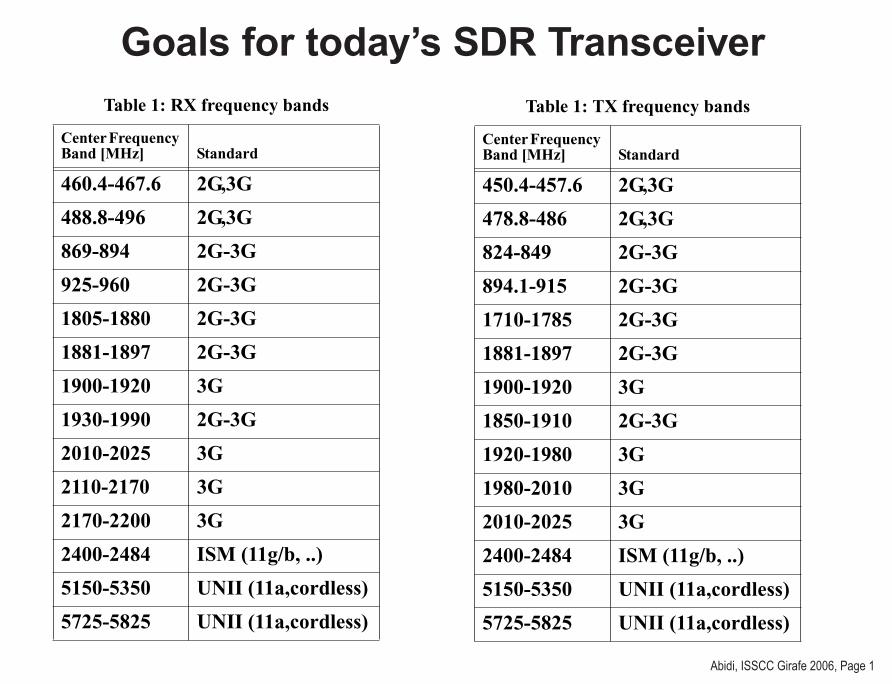
Table 1: RX frequency bands
Center Frequency Band [MHz] Standard
460.4-467.6 2G,3G
488.8-496 2G,3G
869-894 2G-3G
925-960 2G-3G
1805-1880 2G-3G
1881-1897 2G-3G
1900-1920 3G
1930-1990 2G-3G
2010-2025 3G
2110-2170 3G
2170-2200 3G
2400-2484 ISM (11g/b, ..)
5150-5350 UNII (11a,cordless)
5725-5825 UNII (11a,cordless)
Table 1: TX frequency bands
Center Frequency Band [MHz] Standard
450.4-457.6 2G,3G
478.8-486 2G,3G
824-849 2G-3G
894.1-915 2G-3G
1710-1785 2G-3G
1881-1897 2G-3G
1900-1920 3G
1850-1910 2G-3G
1920-1980 3G
1980-2010 3G
2010-2025 3G
2400-2484 ISM (11g/b, ..)
5150-5350 UNII (11a,cordless)
5725-5825 UNII (11a,cordless)
Goals for today’s SDR Transceiver

Abidi, ISSCC Girafe 2006, Page 2
What does the spectrum look like actually?
• Strong signals in only a few bands, and near base stations• Worst-case blocker profi les are pessimistic
Watkins, Bristol U., 2001

What’s wrong with this concept?
• Mitola’s SDR can receive every band and channel concurrently!
• May be important for military, not necessary for civilian uses
Standard Modulation Scheme
ChannelBW (MHz)
GSM GMSK 0.200EDGE 8PSK 0.200
Bluetooth GFSK 1CDMA IS95 QPSK CDMA 1.25
WCDMA/CDMA2000
QPSK/16QAMCDMA
1.25-5
802.11a/g OFDM 20802.11n OFDM 10-20-40
1Good enough to receive one channel at a time, but from any band, with any channel bandwidth, and any
modulation
2Tunes channel of interest to zero IF
3Wideband receiver (no RF preselect)
5 MHz
Digital RX
Modifi ed SDR

What’s inside the Digital Receiver?
fs/2-fs/2 fs/2M-fs/2M
Transfer Function
Frequency0
0
1 ( )T
out inv v t dT
=
1/T 2/T
Ideal anti-alias lter
Sample rate conversion causes aliasing ...
Everything is software controlled - clock rate, no. of taps
Davies, 2000
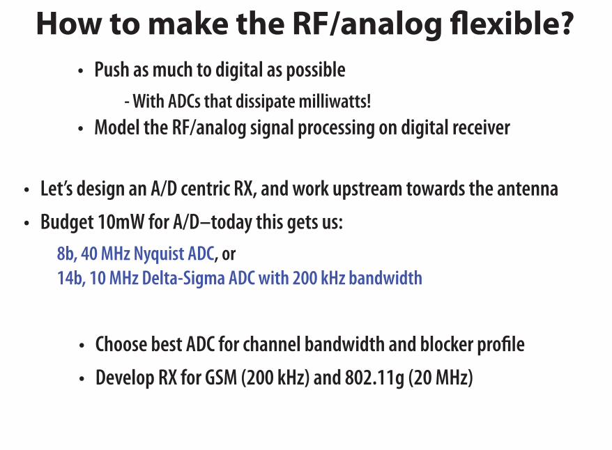
How to make the RF/analog fl exible?
• Push as much to digital as possible - With ADCs that dissipate milliwatts!
• Model the RF/analog signal processing on digital receiver
• Let’s design an A/D centric RX, and work upstream towards the antenna
• Budget 10mW for A/D–today this gets us:8b, 40 MHz Nyquist ADC, or14b, 10 MHz Delta-Sigma ADC with 200 kHz bandwidth
• Choose best ADC for channel bandwidth and blocker profi le
• Develop RX for GSM (200 kHz) and 802.11g (20 MHz)
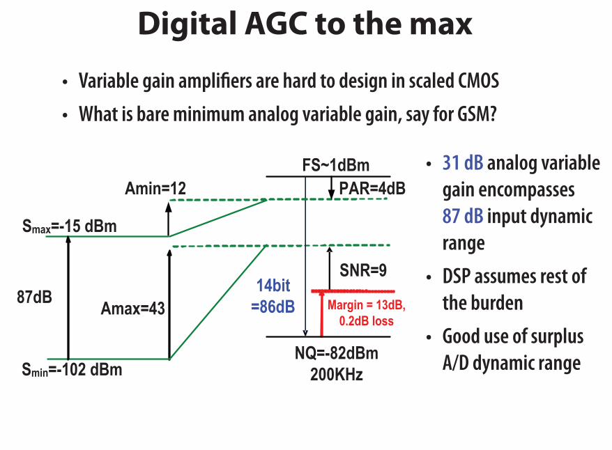
Digital AGC to the max
• Variable gain amplifi ers are hard to design in scaled CMOS
• What is bare minimum analog variable gain, say for GSM?
PAR=4dBAmin=12
Smin=-102 dBm
14bit
=86dB
SNR=9
Amax=43
Smax=-15 dBm
FS~1dBm
NQ=-82dBm
200KHz
Margin = 13dB,
0.2dB loss
87dB
• 31 dB analog variable gain encompasses 87 dB input dynamic range
• DSP assumes rest of the burden
• Good use of surplus A/D dynamic range

Where to sample the wideband input?
• As soon as the signal of interest is at zero IF ...
• Clock-driven discrete-time analog signal processing gives greatest fl exibility
• With 5 GHz-wide input band, what should be the sampling frequency?- Only the channel at zero IF is of interest- Everything else is unwanted- But we’ll need an anti-alias fi lter with 100:1 range in cutoff if we sample 200
kHz to 20 MHz wide channels—impractical

Lowpass Sampler w/ Internal Anti-Alias
• Main-lobe passes wanted signal at DC
• Side-lobes roll off with 20 dB/decade
• Notches @ nfs for anti-aliasing• Wider stop-band with higher fs
Wanted
Ch.
dB
ss s
B=Att*nfs
Windowed Integration Filter
Response
DSP
H f( )gmTsC
------------- πTsf( )sinπTsf
-------------------------=Vin(t) gm Vo(n)
φsφrCφo
[Yuan, 2000]
(n-1)Ts nTs
t=nTs
Vo(n)
gmVin(t)
t
t
Ts Ts
Vo(n+1)
Rectangular Window Integration

Bring Down the Sample Rate (in Analog)
Lindfors, et al., 2003Helsinki University
• Sample rate set by RF pre lter• Unnecessarily high for A/D converter• Must decimate, but with anti-aliasing
• Initial sample rate may be very high, to protect the wanted channel
• A/D conversion at this rate wastes power, as wanted signal band is much lower
• Analog decimation fi lter? Yes ...

Just Enough Analog Filtering
LFilter=-33
dB
9dB
FS~1dBm
Smin+3=-99dBm NQ=-82dBm
200KHz
SNR=9Amax-3=40
Sint=-15 dBm
14bit
=86dB Margin = 13dB,
0.2dB loss
• Filter must be developed based on profi le of in-band and out-of-band blockers
• Remember, there is no RF prefi lter in our SDR

Abidi, ISSCC Girafe 2006, Page 32
Evolution of RX Filter (802.11g) – 1
• Channel of interest lies in 2.4 GHz
band, 20 MHz wide
• Choose initial sample rate of 480 MHz
in windowed integrator (Why? We’ll see
in the next slide)
• Now fi rst aliasing blocker is a strong
CDMA cellular channel
• sinc() alone cannot attenuate it
suffi ciently (–80 dB) across 20 MHz
I
QWideband
LNA
Widetuning LO
Windowedintegration
sampler
fS
-100
-80
-60
-40
-20
0
0 100 200 300 400 500 600
f (MHz)
ISM
2.4GHz2GHz
2G/3G

Abidi, ISSCC Girafe 2006, Page 33
-100
-80
-60
-40
-20
0
0 100 200 300 400 500 600
f (MHz)
Evolution of RX Filter (802.11g) – 2
• Two passive RC poles at the mixer load
gives monotonic attenuation across
frequency (justifi es fs=480 MHz)
• Pole frequencies are programmable
• Small droop in channel bandwidth
around DC
• Filter violates specifi cations between
200-300 MHz
I
QWideband
LNA
Widetuning LO
Prog. RC
poles
Windowedintegration
sampler
fS
Abidi, ISSCC Girafe 2006, Page 34
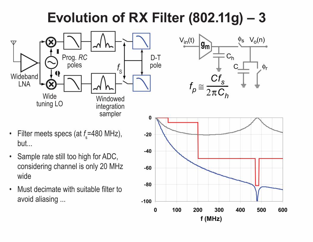
Evolution of RX Filter (802.11g) – 3
• Filter meets specs (at fs=480 MHz),
but...
• Sample rate still too high for ADC,
considering channel is only 20 MHz
wide
• Must decimate with suitable fi lter to
avoid aliasing ... -100
-80
-60
-40
-20
0
0 100 200 300 400 500 600
f (MHz)
I
QWideband
LNA
Widetuning LO
Prog. RC
poles
Windowedintegration
sampler
D-Tpolef
S
Vo(n)Vin(t) gmφs
φrCCh
fpCfs
2πCh--------------≅

Abidi, ISSCC Girafe 2006, Page 35
Evolution of RX Filter (802.11g) – 4
• Decimate by 4
• Now, however, new fi lter spec applies
with 4× more anti-alias notches
• Specifi cation met by sinc2() decimation
FIR fi lter
• Should decimate further to lower power
in ADC — output sample rate 120 MHz
still too high for bandwidth of interest
from 0 ~10 MHz
I
QWideband
LNA
Widetuning LO
D-T sinc2
FIRfS
÷4
-100
-80
-60
-40
-20
0
0 100 200 300 400 500 600
f (MHz)

Abidi, ISSCC Girafe 2006, Page 36
Evolution of RX Filter (802.11g) – 5
• Decimate by 3
• New fi lter spec has 3× more anti-alias
notches
• Specifi cation met by sinc() decimation
FIR fi lter
• Now output sample rate of 40 MHz and
resolution of 8b realizable by ADCs
dissipating ~10 mW
÷4
I
Q
A/D
Con
vers
ion
WidebandLNA
Widetuning LO
D-T sinc
FIRfS
÷3
-100
-80
-60
-40
-20
0
0 100 200 300 400 500 600
f (MHz)
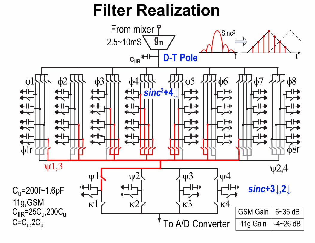
Filter Realizationgm
CIIR
r r
D-T Pole
sinc2+4
sinc+3 ,2
To A/D Converter
From mixer
f t
Sinc2
2.5~10mS
Cu=200f~1.6pF
CIIR=25Cu,200CuC=Cu,2Cu
11g,GSM
ψ1,3
GSM Gain 6~36 dB11g Gain -4~26 dB

The ultimate CMOS mixerVG+VLOV1/forVos6.4mA from 2.5V
VG+VLO
• Passive FETs commutate signal current only
• Current source drive, low impedance buff er => no voltage swing on FETs• Main contributors to 2nd order nonlinearity:
• Low frequency distortion of transconductor: Suppressed by Cc
• Switch offset: Triode operation & low input impedance buffer
• RF-LO feedthrough• IIP2=+77dBm (@-20dBm) • DSB NF~13dB due to gm, flicker noise corner<10KHz (large gate area buffer)

Harmonic mixingUnique to wideband RX
• Hard switching mixer gives high conversion gain—good
• Harmonics in square-wave commutation downconvert in-band channels, e.g. 900 MHz also downconverts 2.7 GHz and 4.5 GHz—BAD!
1
1
0
-45
45
O1O0
O2
OUTRF 2
O1
O0
O2
OUT
[Weldon, ISSCC 2001]
• 3-path mixer better approximates sine• 3rd, 5th harmonic rejection is limited by phase error and gain mismatch
Measured dB3rd Harmonic Rejection 385th Harmonic Rejection 40

Ultimate challenge: Wideband LNA
• CG provides input match• CS to provide extra gain &
single to differential• Input matching forms a 3rd
order maximally-flat ladder filter, embedding bondwire
• 3rd order maximally-flat LC ladder filter as wideband load
• Measured: 18-20dB gain and S11<-10dB over 800M-5GHz
deband low noise amplifier.
RS
1/gm1
Lbond100fF
1.5nH
� �� �
� �� �
� �
� � � � � �
� ain �dB�
• Departs from conventional narrowband RF practices
1416
1820
22
0 2 4 GHz
Gain [dB]

Noise cancellation Feedforward pre-dates feedback
• CG noise is cancelled at diff. output [Bruccoleri, JSSC 2004]
• Noise cancellation has little sensitivity to all parameters and measured NF<3dB [Chehrazi, CICC 2005].
• ~20dB Gain programmability by disabling CS and dumping CG signal current
M1 M2
in1 in2Out
A
A
1
2
3
4
0 2 4 GHz
NF [dB]

Wideband Frequency Tuning
1/2
MUXDigital
3640MHz
5075MHz
Off chipClock
I-Q1/2
1/4820-960M
1.7-2G
2.4-2.49G
5.15-5.35G
• Covers all major bands• 2 VCO, only one is active at a time• 21-33 mA dissipation for different bands
• 3 VCOs can give continuous frequency coverage
• Divide & mux only• No SSB mixers—
unacceptable spurious tones

On-chip SelectivityDisplaces RF preselect fi lter
-120
-80
-40
0 20 40 60 80
0
Input, MHz
dBfS = 72 MHz, 4 & 2 , f
ADC= 9 MHz
Filter specification
Measured response
GSM
Filter specification (WCDMA Band)
fS = 480 MHz, 4 & 3 , f
ADC= 40 MHz
Wanted 802.11g channel
Measuredresponse
-110
-70
-30
10
0 200 400 600Input, MHz
dB
802.11g
Spurious Response
11g@ 22 MHz -60dBrGSM@ 4.7 MHz -74dBr
Currents from 1V
11g Idc 13~28 mAGSM Idc 8~23 mA
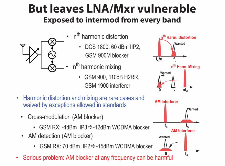
But leaves LNA/Mxr vulnerableExposed to intermod from every band
• Cross-modulation (AM blocker)• GSM RX: -4dBm IIP3 -12dBm WCDMA blocker
Wanted
AM Interferer
fcfa
• nth harmonic mixing• GSM 900, 110dB H2RR,
GSM 1900 interferer
• AM detection (AM blocker)• GSM RX: 70 dBm IIP2 -15dBm WCDMA blocker
nth Harm. DistortionWanted
fcfc/n
nfc
nth Harm. MixingWanted
fc0
• nth harmonic distortion• DCS 1800, 60 dBm IIP2,
GSM 900M blocker
Wanted
AM Interferer
0 fa
• Harmonic distortion and mixing are rare cases and waived by exceptions allowed in standards
• Serious problem: AM blocker at any frequency can be harmful

Final Clock-Programmable SDR Receiver
Full RX Chain SummaryGSM 802.11g
NF (High Gain) [dB] 5 5.5IIP3 (Mid Gain) [dBm] -3.5IIP2 (Mid Gain) [dBm] +65 +67
Power [mW] 18-52 23-57
Active Area ~ 3.8mm2• RX tolerates AM blockers as high as -20dBm with no preselect filter• Still higher linearity is needed from LNA and mixer

Future Research
• Linearity, linearity, linearity!
• Concurrent reception of two or three unrelated bands, sharing hardware
• Full duplex operation such as in CDMA (without RF fi lters?)
• Full system demonstration with digital front-end and baseband—commercial feasibility