EVLSTNRG-1KW: 1 kW SMPS digitally controlled multiphase interleaved converter using ... ·...
66
September 2015 DocID027803 Rev 1 1/66 www.st.com AN4689 Application note EVLSTNRG-1KW: 1 kW SMPS digitally controlled multiphase interleaved converter using the STNRG388A Introduction This application note describes the characteristics and features of the EVLSTNRG-1KW evaluation board, intended for evaluation of the STNRG388A digital controller in offline power conversion applications such as EV battery chargers, UPS and industrial power supplies. The EVLSTNRG-1KW architecture is based on a multiphase interleaved DC-DC converter using the half-bridge SAB (“single active bridge”) topology supporting more than 1000 W of power. The evaluation board can be easily scaled up to 3 kW with 400 V of maximum output voltage. The interleaved topology balances the power through 3 parallel stages. Also, the solution delivers high efficiency during the whole load range by enabling one, two or three stages depending on the load. The STNRG388A power conversion dedicated peripherals (SMEDs) offer the flexibility to drive the interleaved power stages while guaranteeing correct phase realignment during the activation and deactivation of each stage. Thanks to the digital core of the STNRG388A, it is also possible to monitor, control and debug the EVLSTNRG-1KW board via a convenient HyperTerminal control. Figure 1: EVLSTNRG-1KW (power board and control board)
Transcript of EVLSTNRG-1KW: 1 kW SMPS digitally controlled multiphase interleaved converter using ... ·...

September 2015 DocID027803 Rev 1 1/66
www.st.com
AN4689 Application note
EVLSTNRG-1KW: 1 kW SMPS digitally controlled multiphase interleaved converter using the STNRG388A
Introduction This application note describes the characteristics and features of the EVLSTNRG-1KW evaluation board, intended for evaluation of the STNRG388A digital controller in offline power conversion applications such as EV battery chargers, UPS and industrial power supplies.
The EVLSTNRG-1KW architecture is based on a multiphase interleaved DC-DC converter using the half-bridge SAB (“single active bridge”) topology supporting more than 1000 W of power. The evaluation board can be easily scaled up to 3 kW with 400 V of maximum output voltage.
The interleaved topology balances the power through 3 parallel stages. Also, the solution delivers high efficiency during the whole load range by enabling one, two or three stages depending on the load.
The STNRG388A power conversion dedicated peripherals (SMEDs) offer the flexibility to drive the interleaved power stages while guaranteeing correct phase realignment during the activation and deactivation of each stage.
Thanks to the digital core of the STNRG388A, it is also possible to monitor, control and debug the EVLSTNRG-1KW board via a convenient HyperTerminal control.
Figure 1: EVLSTNRG-1KW (power board and control board)

Contents AN4689
2/66 DocID027803 Rev 1
Contents
1 Main characteristics and circuit description .................................................... 6
1.1 HB SAB converter features ......................................................................... 6
1.2 Flyback converter features .......................................................................... 7
1.3 Related documents ..................................................................................... 7
1.4 Block diagram ............................................................................................. 7
2 Board description ............................................................................................... 8
2.1 Power board ................................................................................................ 8
2.2 Control board ............................................................................................ 10
3 Use of the STNRG388A .................................................................................... 13
3.1 Resource allocation ................................................................................... 13
3.2 Schematic block diagram .......................................................................... 13
3.3 Protection features and dedicated algorithms ........................................... 14
3.3.1 Soft-start procedure ..................................................................................... 15
3.3.2 Soft-stop procedure after a 1st level OCP .................................................... 15
3.3.3 Auto-restart feature after a 2nd level OCP ................................................... 15
3.3.4 Redundant and latched OVP ........................................................................ 15
3.3.5 Auxiliary voltage fault on secondary side ..................................................... 15
3.3.6 Input voltage brownouts ............................................................................... 16
3.3.7 Startup voltage ............................................................................................. 16
4 STNRG388A control board .............................................................................. 17
4.1 Description ................................................................................................ 17
4.2 Pinout ........................................................................................................ 17
5 Functional check .............................................................................................. 19
6 UART interface .................................................................................................. 31
6.1 Commands ................................................................................................ 33
6.1.1 checkrange ................................................................................................... 33
6.1.2 currfreq ......................................................................................................... 34
6.1.3 help .............................................................................................................. 34
6.1.4 lpm ............................................................................................................... 34
6.1.5 maxfreq ........................................................................................................ 34
6.1.6 minfreq ......................................................................................................... 35
6.1.7 nphases ....................................................................................................... 35
6.1.8 ocp1ph1 ....................................................................................................... 35
6.1.9 ocp1ph2 ....................................................................................................... 36
6.1.10 ocp1ph3 ....................................................................................................... 36
6.1.11 ocp2delay ..................................................................................................... 36
6.1.12 openloop ...................................................................................................... 36

AN4689 Contents
DocID027803 Rev 1 3/66
6.1.13 RESETsystem .............................................................................................. 37
6.1.14 reseteeprom ................................................................................................. 37
6.1.15 resteedata .................................................................................................... 38
6.1.16 seteedata ..................................................................................................... 38
6.1.17 setthmax ...................................................................................................... 38
6.1.18 setthmin ....................................................................................................... 38
6.1.19 softstart ........................................................................................................ 39
6.1.20 status ........................................................................................................... 39
6.1.21 threshold ...................................................................................................... 40
6.1.22 trace ............................................................................................................. 41
6.1.23 vfb ................................................................................................................ 42
6.1.24 vfbol ............................................................................................................. 42
6.1.25 vff ................................................................................................................. 43
6.1.26 vin ................................................................................................................ 43
6.1.27 vinbo1 .......................................................................................................... 43
6.1.28 vinbo2 .......................................................................................................... 44
6.1.29 vinstart ......................................................................................................... 44
6.1.30 vers .............................................................................................................. 44
6.2 How to set phase shedding thresholds ..................................................... 44
7 Efficiency measurements ................................................................................ 47
8 Appendix ........................................................................................................... 49
8.1 Schematic diagrams .................................................................................. 49
8.2 HB-SAB power transformer specification .................................................. 52
8.2.1 General description and characteristics ....................................................... 52
8.2.2 Electrical characteristics ............................................................................... 53
8.2.3 Mechanical aspect and pin numbering ......................................................... 53
8.2.4 Manufacturer ................................................................................................ 54
8.3 Auxiliary flyback transformer specification ................................................ 54
8.3.1 General description and characteristics ....................................................... 54
8.3.2 Electrical characteristics ............................................................................... 55
8.3.3 Mechanical aspect and pin numbering ......................................................... 55
8.3.4 Manufacturer ................................................................................................ 57
8.4 Bill of materials .......................................................................................... 57
9 Revision history ................................................................................................ 65

List of tables AN4689
4/66 DocID027803 Rev 1
List of tables Table 1: Overall efficiency measured at 390 Vdc of input voltage ........................................................... 47 Table 2: HB-SAB power transformer winding characteristics ................................................................... 53 Table 3: Auxiliary flyback transformer winding characteristics ................................................................. 55 Table 4: Bill of materials ........................................................................................................................... 57 Table 5: Document revision history .......................................................................................................... 65

AN4689 List of figures
DocID027803 Rev 1 5/66
List of figures Figure 1: EVLSTNRG-1KW (power board and control board) ................................................................... 1 Figure 2: Block diagram of the system ....................................................................................................... 7 Figure 3: Block diagram of a multi-phase interleaved DC-DC resonant converter .................................... 8 Figure 4: Single phase of the HB-SAB topology ......................................................................................... 9 Figure 5: Block diagram of a multi-phase interleaved DC-DC resonant converter with 2 phases active ... 9 Figure 6: Signals generated by the STNRG388A to handle half-bridge drivers ....................................... 11 Figure 7: Schematic block diagram .......................................................................................................... 14 Figure 8: Control board view ..................................................................................................................... 17 Figure 9: Pinout of the control board connector ....................................................................................... 18 Figure 10: Top view of the power board ................................................................................................... 19 Figure 11: Three active phases with 120° of phase shift .......................................................................... 20 Figure 12: Two active phases with 90° of phase shift .............................................................................. 21 Figure 13: One active phase ..................................................................................................................... 21 Figure 14: Resonant stage waveforms ..................................................................................................... 22 Figure 15: Resonant tank current for each phase and output current, at full load ................................... 22 Figure 16: Phase shedding, from 3 to 2 active phases ............................................................................ 23 Figure 17: Phase shedding, from 2 to 1 active phases ............................................................................ 23 Figure 18: Phase shedding, from 1 to 2 active phases ............................................................................ 24 Figure 19: Phase shedding, from 2 to 3 active phases ............................................................................ 24 Figure 20: Full load startup; primary currents and output current ............................................................ 25 Figure 21: No-load startup; primary currents and output voltage ............................................................. 25 Figure 22: Soft-stop after a 1st level OCP with threshold sets to 8 (0.65 V) ............................................ 26 Figure 23: Soft-stop after a 1st level OCP with threshold sets to 10 (0.82 V) .......................................... 27 Figure 24: No-load operation .................................................................................................................... 27 Figure 25: Load transition between 7.5 A and 0.15 A of output current ................................................... 28 Figure 26: Zero to full load transition ........................................................................................................ 29 Figure 27: Zero to full load transition – current detail ............................................................................... 29 Figure 28: Full to zero load transition ....................................................................................................... 30 Figure 29: Full to zero load transition – current detail .............................................................................. 30 Figure 30: Initial prompt ............................................................................................................................ 31 Figure 31: “help” command ....................................................................................................................... 32 Figure 32: “help help” command ............................................................................................................... 33 Figure 33: “status” command ................................................................................................................... 40 Figure 34: “threshold g” and “threshold v g” commands ........................................................................... 41 Figure 35: “vfbol set” command ................................................................................................................ 43 Figure 36: Graph of the overall efficiency of the system .......................................................................... 48 Figure 37: Power board schematic diagram – power section and feedback ............................................ 49 Figure 38: Power board schematic diagram – auxiliary supply and protections ...................................... 50 Figure 39: Power board schematic diagram – connector to control board ............................................... 51 Figure 40: Power board schematic diagram – gate driver sub-circuit ...................................................... 51 Figure 41: Control board schematic diagram ........................................................................................... 52 Figure 42: HB-SAB power transformer overall drawing ............................................................................ 53 Figure 43: HB-SAB power transformer specification – drawing ............................................................... 54 Figure 44: Auxiliary flyback transformer overall drawing .......................................................................... 55 Figure 45: Auxiliary flyback transformer specification – drawing .............................................................. 56 Figure 46: Auxiliary flyback transformer construction ............................................................................... 57

Main characteristics and circuit description AN4689
6/66 DocID027803 Rev 1
1 Main characteristics and circuit description The main features of the SMPS are:
Input voltage range: 350-420 Vdc
Full-load power: 1000 W
CC/CV output regulation
Output voltage regulation: 133 V ± 2.5%
Output current regulation: 7.5 A ± 5%
Minimum output current for each phase without burst mode: approx. 1 A
Maximum output current for each phase: 2.5 A
Interleaving architecture
Standby consumption with no load: 425 mW
Efficiency: above 90% from 1% to full load
Peak efficiency: 96.5% at full load
Safety: according to EN60950
Power board size: 20.7x16.5 mm, 50 mm max component height from PCB
Control board size: 6.9x5 mm, vertical mounting
Power board PCB: double layer, 35 µm, mixed PTH/SMT
Control board PCB: double layer, 35 µm, mixed PTH/SMT
System configurable through UART I/F
Status LEDs for protection features and active phases
Firmware version: 1.1
The circuit board is composed of two sections:
1. A 3 W flyback-topology auxiliary supply based on the Viper06H high-voltage switcher for offline applications. This auxiliary converter delivers 15 V/0.1 A for the primary side to supply drivers and control logic and ±7.5 V/0.1 A on the secondary side to supply the analog feedback compensation.
2. The main converter is composed of three half-bridge SAB converters controlled by the STNRG388A digital controller which manages output power by changing the switching frequency and enabling or disabling phases.
The drive function for the discrete MOSFETs of the main converter is provided by the L6391. This dedicated companion driver also integrates smart shutdown functions with an internal analog comparator to quickly trigger several protection features. A precise reference voltage reduces the auxiliary supply voltage to provide the STNRG388A up to 30 mA at 3.3 V.
1.1 HB SAB converter features
Frequency control with min. & max. frequency limitation
Fixed dead-time
Digital voltage feed-forward
High phase shift precision
Phase shedding to increase efficiency at low loads
CC/CV compensation with single feedback signal
2 brownout levels and minimum startup voltage
Protection features:
2-level overcurrent protection
Redundant overvoltage protection
Auxiliary voltage fault on secondary side
soft-start and soft-stop after a 1st level OCP event

AN4689 Main characteristics and circuit description
DocID027803 Rev 1 7/66
Configurable auto-restart delay after a 2nd level OCP event
1.2 Flyback converter features
Fixed switching frequency (115 kHz) with frequency jittering
CCM – DCM operation according to mains voltage and load amount
1.3 Related documents
For complete information regarding the STNRG388A digital controller, please refer to the STNRG388A datasheet.
1.4 Block diagram
The overall system architecture is summarized in diagram below.
Figure 2: Block diagram of the system
Board description AN4689
8/66 DocID027803 Rev 1
2 Board description
2.1 Power board
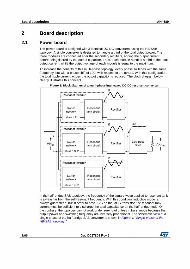
The power board is designed with 3 identical DC-DC converters, using the HB-SAB topology. A single converter is designed to handle a third of the total output power. The three modules are connected after the secondary rectifiers, adding the output current before being filtered by the output capacitor. Thus, each module handles a third of the total output current, while the output voltage of each module is equal to the maximum.
To increase the benefits of this multi-phase topology, every phase switches with the same frequency, but with a phase shift of 120° with respect to the others. With this configuration, the total ripple current across the output capacitor is reduced. The block diagram below clearly illustrates this concept.
Figure 3: Block diagram of a multi-phase interleaved DC-DC resonant converter
In the half-bridge SAB topology, the frequency of the square wave applied to resonant tank is always far from the self-resonant frequency. With this condition, inductive mode is always guaranteed, but in order to have ZVS on the MOS transistor, the resonant tank current must be sufficient to discharge the total capacitance on the half-bridge node. On the contrary, the topology cannot work under zero load unless in burst mode because the output power and switching frequency are inversely proportional. The schematic view of a single phase of the half-bridge SAB converter is shown in Figure 4: "Single phase of the HB-SAB topology ".

AN4689 Board description
DocID027803 Rev 1 9/66
Figure 4: Single phase of the HB-SAB topology
In order to increase efficiency, or when frequency control is not sufficient to handle the output power, one or more phases must be disabled to regulate the output current: this is known as “phase shedding”. The control board manages this situation by keeping one or two phases active to regulate the output current. To reduce output current ripple across the output capacitor when two phases are active, the phase shift must be set to 90° eliminate current ripple, as shown in Figure 5: "Block diagram of a multi-phase interleaved DC-DC resonant converter with 2 phases active".
Figure 5: Block diagram of a multi-phase interleaved DC-DC resonant converter with 2 phases active
On the primary side, the L6391 drivers are used to manage the half-bridge topology. These devices allow the use of only one pin to handle the high-side and low-side MOS transistors,

Board description AN4689
10/66 DocID027803 Rev 1
adding a fixed dead time before switching from one to the other. They also have a standby/shutdown pin, which is useful for disabling the driver externally, and an internal comparator usually connected to the current sense, to intelligently shut down the driver when overcurrent protection is triggered.
There are two overcurrent protection levels on the primary side: the first, managed by the control board, is triggered when the total average current exceeds a preset value; the second, managed by the power board hardware, is triggered and latched when the resonant tank peak current exceeds a safe value set in the hardware. This condition is both sent to the control board and connected to the internal comparator of the L6391 so as to immediately disable the drivers when this situation occurs.
Three transformers are used to isolate the primary from the secondary side, making the modules independent.
On the secondary side, full bridge rectifiers rectify the secondary current; then each current is added to the others and filtered by the output capacitor. A TSM1013A constant voltage and constant current controller is used for CC/CV control via sense resistors for the output current and divider resistors for the output voltage. Through an optocoupler, a single feedback signal is passed to the primary side, which goes directly to the control board in order to achieve closed-loop control. Another optocoupler is dedicated to providing overvoltage protection and auxiliary voltage fault information to the primary side. When the OVP is triggered, however, the information is latched and passed with the optocoupler used for the feedback, in order to achieve redundant protection even when the dedicated optocoupler fails.
The VIPER06HS is used to supply primary and secondary side components. On the primary side, a 3.3 V linear regulator also supplies the control board and the 3.3 V signal.
With a 50-pin connector, all relevant signals are sent to the control board to implement a closed-loop system and to handle all events coming from the power board.
2.2 Control board
The core of the control board is the high performance STNRG388A digital controller for power conversion applications, a featuring 6 state machine event driver peripheral with independent programmable PWM output pulse generator, 4 analog comparators, 8 channels with 10-bit resolution A/D converters, and 12 multi-function GPIO pins.
It is programed to generate 3 PWM signals with 50% duty cycle and the same frequency, but with a phase shift of 120°, sent to the L6391 half-bridge driver. Phase shift accuracy is guaranteed by the implemented architecture. With f0 the half-bridge frequency, one SMED switching at 3*f0 is used to synchronize the other 3 SMEDs. Synchronization is performed on the edges of the triple-frequency PWM signal, ensuring that phase shift between one SMED and another is always 120°, as shown in Figure 6: "Signals generated by the STNRG388A to handle half-bridge drivers". Also, frequency adjustments are done by changing the switching frequency of the synchronization SMED, making control as safe and easy as possible.

AN4689 Board description
DocID027803 Rev 1 11/66
Figure 6: Signals generated by the STNRG388A to handle half-bridge drivers
Moreover, each SMED is sensitive to the high level signal of the previous SMED to prevent switching noise desynchronizing the system.
The feedback signal is sampled and used to modify the switching frequency of the synchronization SMED and, therefore, of the half-bridges.
When the system is in CC regulation, all the phases must be kept enabled to reduce the output current ripple.
Conversely, when the system is in CV regulation, if output current decreases, the control board must disable one or more phases (known as "phase shedding") in order to maintain high efficiency. When at a rated output power, the overall efficiency at 3 active phases is less than the same for 2 active phases, the control board disables one phase and configures the remaining two active phases with a phase shift of 90°. This new phase shift is useful to limit output current ripple.
During phase shedding, the system is reorganized: the synchronization SMED switches at twice f0, while the other two SMEDs are reconfigured on-the-fly to switch with a phase shift of 90°.
To maintain high efficiency if the output current again decreases, the system passes to only one active phase or to zero phases when it is not possible to regulate output voltage with one phase switching at the maximum frequency. This implements shallower or deeper burst-mode depending on the load. Vice versa, when load increases towards the maximum current, the system is reconfigured to work with 1 phase or 2 phases at 90° or 3 phases at 120°.
Also, the input voltage is sampled and used to handle brownout conditions and to perform digital voltage feed-forward, in order to obtain a feedback signal that is independent of the input voltage and only related to the output power, to handle phase shedding directly from this signal.
Two brownout threshold levels can be set in the firmware. This enhancement depends strictly on the SAB topology. In fact, when the system operates at maximum power, the minimum input voltage threshold is 350 V, as per specification. This threshold is also the first brownout threshold level. However, when the power is less than the maximum, the system can probably regulate the output even if the input voltage is less than this value. Thus, a second brownout threshold level below 350 V is set. If this second threshold is

Board description AN4689
12/66 DocID027803 Rev 1
exceeded, the system shuts down immediately. But if the system is in the first level brownout condition and the control loop does not require more power than what the system can supply, the system is not stopped and the output continues to be regulated.
One analog comparator is used to sense the sum of the average resonant tank current and sense the first level OCP: if this happens, the control increases the frequency in an attempt to remove the first level OCP signal. This procedure is called soft stop because the control system linearly increases the frequency towards the maximum.
The second level OCP is connected to a digital input, because the threshold is hardware set. When this occurs, the control board shuts down all active phases, disabling the MOSFET drivers. However, it is important to remember that the L6391 internal comparator already shuts down the driver when the control board senses this condition.
When the system starts up, a safe soft-start is implemented: the system starts with only one phase active, at the maximum frequency. The frequency decreases roughly linearly to the minimum in order to approximate a linear output power increase. If the minimum frequency is reached and control requires more power, the phase shedding procedure is called and additional phases are activated until the power required by the control loop is the same as the soft-start power. Here, the soft-start procedure is shut down and the control loop is closed.
After a first level OCP event, to avoid dangerous frequency steps if the system returns directly from a soft-stop procedure to the closed loop control, the soft-start procedure is also invoked in order to allow the system to gradually recover regulation.
UART is used to connect the control board to a PC, to view or set numerous system parameters using HyperTerminal or equivalent software, including 1st level OCP thresholds, phase shedding thresholds, maximum and minimum switching frequencies, current switching frequencies, feedback signals, input voltage brownout thresholds, etc.
UART can also be used to open the control loop and manage feedback signals directly from the command line, which is useful to set thresholds or to observe how the system works in certain conditions.
All changed parameters are saved only to RAM and are lost after a system reset. There are some commands to store them in the EEPROM memory, or to recall them after they have been changed. After a system reset, parameters are always loaded from EEPROM; an 8-bit CRC ensures that this process is performed correctly, otherwise default system parameters are loaded.
UART can also be used to check system status (OCP, active phases, brownout, open-loop mode, etc.), either with a user request or through an auto-trace of working conditions. Auto-trace can be configured individually for the most important parameters.
AN4689 Use of the STNRG388A
DocID027803 Rev 1 13/66
3 Use of the STNRG388A
3.1 Resource allocation
The following is a list of the STNRG388A resources used to implement the system control algorithm:
SMED0: used as PWM for the 1st phase; in this document, PWM signal is called PWM0.
SMED1: used as PWM for the 3rd phase; in this document, PWM signal is called PWM2.
SMED2: used as PWM for the 2nd phase; in this document, PWM signal is called PWM1.
SMED5: used to synchronize all above SMEDs; in this document, PWM signal is called SYNC.
DIGIN0: used to acquire 2nd level OCP, OVP and auxiliary voltage fault from the secondary side.
DIGIN1: connected to SMED2 output, for synchronization.
DIGIN2: connected to SMED5 output, for synchronization.
DIGIN3: connected to SMED5 output, for synchronization.
GPIO0: UART TX signal.
GPIO1: UART RX signal.
GPIO2: enable for the half-bridge driver of the 1st phase.
GPIO3: enable for the half-bridge driver of the 2nd phase.
GPIO4: enable for the half-bridge driver of the 3rd phase.
GPIO5: primary auxiliary voltage on/off signal for half-bridge drivers.
CPP1: used to sense the total average primary current for 1st level OCP detection.
CPP2: used for primary auxiliary voltage brownout during startup phase.
CPP3: used to wake up the STNRG388A during the burst mode operation, connected to the feedback signal from the secondary side.
ADC0: used to sample feedback signal and realize closed loop control and phase shedding.
ADC1: used to sample input voltage.
In the STNRG388A documents, PWMx is used to refer to SMEDx output. This convention is not used in this document. Here, PWMx refers to the single control signal for the half-bridge driver, where “x” is one of the three phases (0, 1 or 2).
3.2 Schematic block diagram
The complete block diagram of the system with a simplified schematic view is shown in Figure 7: "Schematic block diagram".
The primary auxiliary voltage as well as GPIO5 and CPP2 used to manage this voltage are not shown in this diagram, but in the STNRG388A device block.

Use of the STNRG388A AN4689
14/66 DocID027803 Rev 1
Figure 7: Schematic block diagram
3.3 Protection features and dedicated algorithms
Many protection features and dedicated algorithms are implemented in the STNRG388A code. The most important are described here.
The UART interface can be used to modify some protection parameters and to track the status of the system. For further information, please refer to Section 6: "UART interface".
When the converter is switched off for 2nd level OCP, OVP, or 2nd level brownout, a red LED on the primary side is switched on to indicate that the converter is currently shut down.

AN4689 Use of the STNRG388A
DocID027803 Rev 1 15/66
3.3.1 Soft-start procedure
A soft-start procedure is always called after a power-on-reset, after having executed the soft-stop procedure, or when certain setting are modified through the UART interface.
The soft-start procedure ensures that the system catches the regulation safely. The procedure monitors the feedback signal from the secondary side and decreases the output frequency almost linearly. When the frequency that the procedure would impose is lower than that requested by the feedback signal, the soft-start procedure ends and the loop is closed. The feedback signal is then used to set the switching frequency of the half-bridges.
3.3.2 Soft-stop procedure after a 1st level OCP
A soft-stop procedure is called after a 1st level OCP. If this condition occurs, the system tries to recover overcurrent protection by increasing the output frequency. When the overcurrent protection elapses, the soft-start procedure is invoked in order to catch the regulation gradually.
Usually, if phase shedding thresholds are set correctly and the 1st level OCP threshold is high enough, the 1st level OCP procedure is never called. There are only two cases where the 1st level OCP protection is triggered: the first is when the system is working in open-loop mode for a number of active phases or by a feedback signal, described in Section 6.1.12: "openloop". In this condition, the user can manage the number of active phases and/or the feedback signal directly using the terminal software through the UART interface, and the average current for which each phase can exceed the 1st level OCP threshold, triggering the protection.
The second case occurs when the control loop has not yet closed: this can happen during the startup phase or when the output passes from open circuit to a short circuit. In these cases, neither the output voltage nor the output current are regulated and the system tries to recover by setting a very low switching frequency. This can trigger the protection, depending on the thresholds set.
1st level OCP thresholds differ for the number of active phases and can be set using the UART interface.
3.3.3 Auto-restart feature after a 2nd level OCP
If the primary current exceeds a safe hardware set value, the 2nd level OCP is triggered and the system is immediately shut down. The STNRG388A keeps all phases switched off for a
time delay settable through the UART interface with the ocp2delay command. After that,
the system is auto-restarted. For more information about how to set the time delay, please refer to Section 6: "UART interface", in particular Section 6.1.11: "ocp2delay".
3.3.4 Redundant and latched OVP
If the output voltage exceeds a hardware set threshold, the overvoltage protection is triggered and the information is passed to the primary side through an optocoupler. The redundant protection through the feedback optocoupler ensures that the system shuts down all the phases even if the dedicated optocoupler fails. In any case, the protection is latched at the secondary side and it is necessary to recycle the input voltage to restart the system. A red LED on the secondary side is switched on when the protection is triggered.
3.3.5 Auxiliary voltage fault on secondary side
The same optocoupler for the OVP is used to sense the auxiliary voltage on the secondary side. If the auxiliary voltage on the secondary side is not ready or there is a fault, the protection keeps the system switched off. This protection is not latched.
Use of the STNRG388A AN4689
16/66 DocID027803 Rev 1
A green LED on the secondary side is switched on as soon as the auxiliary voltage on the secondary side is ready. This is switched off if an overvoltage protection event occurs.
3.3.6 Input voltage brownouts
There are two levels of input voltage brownout: the 1st brownout level occurs if the input voltage falls below a set value (350 V by default, in order to respect the minimum input voltage specification). This condition only sets an internal signaling bit. The bit is reset after a hysteresis of 5 V.
The 2nd level brownout threshold is 300 V by default. If the input voltage falls below this voltage, the system shuts down immediately and waits for the input voltage to rise higher than the startup threshold.
If the input voltage is between the two thresholds, the system runs normally but has less power capability. If the feedback signal requests less power than the maximum the system can source under these conditions, the system sources that power as normal. But, if the feedback signal requests more power than the maximum the system can source with that input voltage, the system shuts down and enters the same situation as if the 2nd brownout level was reached.
Both input voltage brownout thresholds can be set using the UART interface.
Depending on phase shedding thresholds, if the system is working between the two brownout levels, it could jump between different active phases to keep the output regulated. This is normal because it has less power capability and the switching frequency must be lower than the minimum to keep the output regulated with the same number of active phases. In any case, the 1st level brownout condition is supposed to be a transient situation.
3.3.7 Startup voltage
After a power-on reset, a system reset, or a 2nd level brownout condition, the system does not start unless the input voltage is higher than the startup threshold. This voltage is higher than the 1st level brownout threshold. The default value of the startup voltage is 380 V and can be modified using the UART interface.

AN4689 STNRG388A control board
DocID027803 Rev 1 17/66
4 STNRG388A control board
4.1 Description
The STNRG388A control board shown in Figure 8: "Control board view" is designed to provide maximum flexibility when using it with new designs.
Figure 8: Control board view
The most relevant signals are routed through the 50-pin connector: 8 ADC inputs, each with an analog ground; 4 analog comparators, 3 with analog grounds and 1 with external reference; 5 SMED outputs, 3 digital inputs and 6 GPIOs, with 8 digital grounds; divided power supply for digital and analog sections, each with its own ground.
The entire connector can be decoupled by the STNRG388A pins and the default configuration can be easily changed. In fact, each pin has an easily-removable 0 Ω resistor in series. Also, interconnections made inside the board (output of the synchronization SMED with digital inputs DIG2 and DIG3, and PWM1 with DIG1) have the same 0 Ω resistors in series in order to decouple them easily for new new designs.
In order to remove high frequency noise, each analog input has a low pass filter in series.
A reset push button is installed to reset the STNRG388A asynchronously. There is also the possibility to install a quartz oscillator if it is necessary to implement high precision temporization in other applications.
All STNRG388A pins are accessible with 2.54 mm pin header connectors, to facilitate checking their value with a probe.
In order to program the STNRG388A, a SWIM interface is accessible with a 2.54 mm 4-pin header connector.
A 3.5 mm jack connector is installed to connect the UART interface to a personal computer, to manage and configure the STNRG388A. Finally, a power supply connector is present to all external supply.
4.2 Pinout
The connector pinout is shown in Figure 9: "Pinout of the control board connector".

STNRG388A control board AN4689
18/66 DocID027803 Rev 1
Figure 9: Pinout of the control board connector
As can be observed, analog and digital pins are divided in the connector in order to reduce interference between analog and digital signals.

AN4689 Functional check
DocID027803 Rev 1 19/66
5 Functional check Referring to Figure 10: "Top view of the power board", from top-left to bottom-left we have the input voltage connector (marked “IN”), the auxiliary primary supply OK LED (D1), the active phase status LED (D2, D3 and D4) the auxiliary primary power supply output (J2”), and the protection status LED (D8). On the right-hand side, the OVP LED (D6), the output voltage connector (J3) and the auxiliary secondary supply OK LED (D7).
Figure 10: Top view of the power board
First, the STNRG388A control board must be connected to the power board through the 50-pin connector. Then, after having connected the board through the input voltage connector (IN) to the HV-DC bus (maximum 450 V) and having powered up the board, the system starts if the input voltage is higher than the input voltage startup threshold. The integrated VIPER regulator starts operating if the input voltage is higher than about 45 V and regulates all the auxiliary supplies. Both the auxiliary supply OK LEDs (D1 and D7) must switch on after having powered up the VIPER regulator. The auxiliary primary supply output connector J2 can be used to monitor the auxiliary primary supply.
Through LEDs D2, D3 and D4, the actual number of active phases can be monitored.
If for any reason the board switches off, the protection status LED D8 switches on to indicate that the board is currently in a protection state: this can be 2nd level brownout protection, 2nd level overcurrent protection, or overvoltage protection on the secondary side. In the last case, the OVP LED D6 on the secondary side also switches on to indicate that the overvoltage protection is triggered (and latched) and the input voltage must be recycled to restart the board. Also, when the OVP LED switches on, the auxiliary secondary supply OK LED D7 switches off.
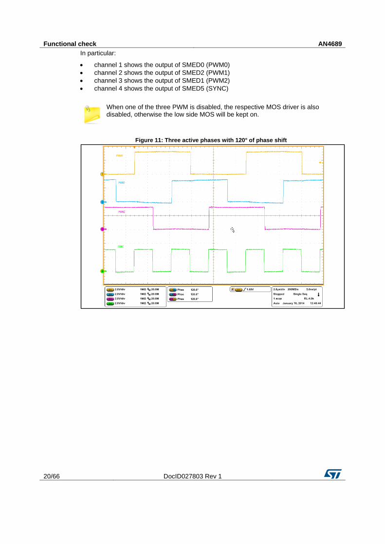
Figure 11: "Three active phases with 120° of phase shift", Figure 12: "Two active phases with 90° of phase shift" and Figure 13: "One active phase" show the SMED outputs for the three phase shedding configurations.
Functional check AN4689
20/66 DocID027803 Rev 1
In particular:
channel 1 shows the output of SMED0 (PWM0)
channel 2 shows the output of SMED2 (PWM1)
channel 3 shows the output of SMED1 (PWM2)
channel 4 shows the output of SMED5 (SYNC)
When one of the three PWM is disabled, the respective MOS driver is also disabled, otherwise the low side MOS will be kept on.
Figure 11: Three active phases with 120° of phase shift

AN4689 Functional check
DocID027803 Rev 1 21/66
Figure 12: Two active phases with 90° of phase shift
Figure 13: One active phase
Figure 14: "Resonant stage waveforms" shows the waveforms for a single phase half-bridge SAB converter. Channel 1 shows the half-bridge node, Channel 2 shows the low-side gate voltage referred to ground, Channel 3 shows the high-side gate voltage referred to the half-bridge node, and channel 4 shows the current flowing into the LC tank.

Functional check AN4689
22/66 DocID027803 Rev 1
Figure 14: Resonant stage waveforms
Figure 15: "Resonant tank current for each phase and output current, at full load" shows the three currents flowing through each LC tank and the output current before being filtered by the output capacitor, at full load condition.
Figure 15: Resonant tank current for each phase and output current, at full load
The phase shedding procedure is shown in the following graphs from Figure 16: "Phase shedding, from 3 to 2 active phases" to Figure 19: "Phase shedding, from 2 to 3 active
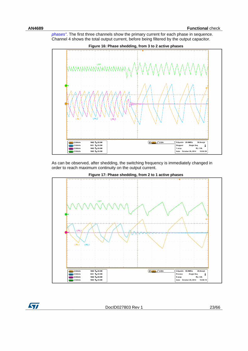
AN4689 Functional check
DocID027803 Rev 1 23/66
phases". The first three channels show the primary current for each phase in sequence. Channel 4 shows the total output current, before being filtered by the output capacitor.
Figure 16: Phase shedding, from 3 to 2 active phases
As can be observed, after shedding, the switching frequency is immediately changed in order to reach maximum continuity on the output current.
Figure 17: Phase shedding, from 2 to 1 active phases

Functional check AN4689
24/66 DocID027803 Rev 1
Figure 18: Phase shedding, from 1 to 2 active phases
Figure 19: Phase shedding, from 2 to 3 active phases
The next two graphs show the full and no-load startup, with the soft-start feature: channels 1, 2 and 3 show the three primary currents, channel 4 shows the total output current before being filtered in Figure 20: "Full load startup; primary currents and output current", and the output voltage in Figure 21: "No-load startup; primary currents and output voltage".

AN4689 Functional check
DocID027803 Rev 1 25/66
Figure 20: Full load startup; primary currents and output current
As can be observed, thanks to the soft-start feature, the output frequency is decreased linearly to allow a linear increase in the output current, until either the output current or the output voltage reaches the regulation. During startup, the 1st level OCP may be triggered, because the output voltage and the output current are not regulated.
Figure 21: No-load startup; primary currents and output voltage
Figure 22: "Soft-stop after a 1st level OCP with threshold sets to 8 (0.65 V)" and Figure 23: "Soft-stop after a 1st level OCP with threshold sets to 10 (0.82 V)" show the soft-stop feature after a 1st level OCP.

Functional check AN4689
26/66 DocID027803 Rev 1
The OCP is simulated enabling the open loop control mode for a number of active phases, setting 2 active phases and executing a load transition from 3.75 A to 7.4 A. In these conditions, the system cannot supply 7.4 A with 2 active phases, so the 1st level OCP is triggered and the protection is activated.
As can be observed, the switching frequency increases linearly to decrease the current linearly, until the internal analog comparator, which senses the overcurrent protection, switches off. Then the soft-start procedure linearly increases the frequency and the output current becomes regulated on the 1st level OCP threshold, until the feedback signal request for lower power.
The 1st level overcurrent protection acts as if the system is controlled by the average of the
primary current. The current level is set using the UART interface through the ocp1ph2
command, described in Section 6.1.9: "ocp1ph2". Figure 22: "Soft-stop after a 1st level OCP with threshold sets to 8 (0.65 V)" and Figure 23: "Soft-stop after a 1st level OCP with threshold sets to 10 (0.82 V)" only differ on the threshold set: in the first graph the internal level is set to 8 (which corresponds to a voltage threshold of 0.65 V), while it is set to 10 (or 0.82 V) in the letter. As can be observed, the average of the primary current and hence the total output current are different and depend proportionally on the threshold settings.
Figure 22: Soft-stop after a 1st level OCP with threshold sets to 8 (0.65 V)

AN4689 Functional check
DocID027803 Rev 1 27/66
Figure 23: Soft-stop after a 1st level OCP with threshold sets to 10 (0.82 V)
Figure 24: "No-load operation" shows no-load operation when the system goes into a deep burst mode.
In particular, the currents on the resonant tanks during burst and the output voltage are shown.
Figure 24: No-load operation

Functional check AN4689
28/66 DocID027803 Rev 1
Figure 25: "Load transition between 7.5 A and 0.15 A of output current" shows the load transition between full load (7.5 A) and 0.15 A current. Channel 4 shows the output voltage drops during these transitions.
Figure 25: Load transition between 7.5 A and 0.15 A of output current
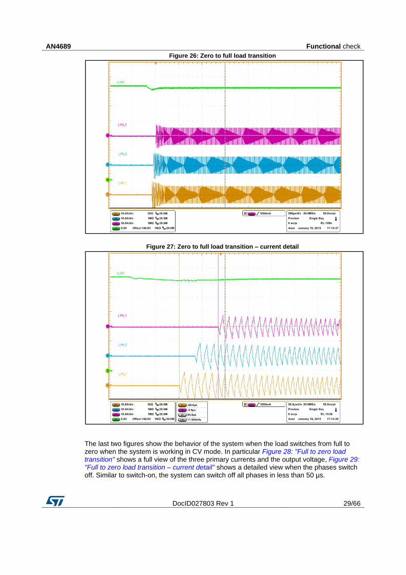
Figure 26: "Zero to full load transition" and Figure 27: "Zero to full load transition – current detail" show the behavior of the system when the load switches from zero to full when the system is working in CV mode. Channel 4 shows the output voltage and its drop during this transition.
Figure 27: "Zero to full load transition – current detail" shows a detailed view of the currents: the system switches from zero to all phases active in less than 100 µs.
AN4689 Functional check
DocID027803 Rev 1 29/66
Figure 26: Zero to full load transition
Figure 27: Zero to full load transition – current detail
The last two figures show the behavior of the system when the load switches from full to zero when the system is working in CV mode. In particular Figure 28: "Full to zero load transition" shows a full view of the three primary currents and the output voltage, Figure 29: "Full to zero load transition – current detail" shows a detailed view when the phases switch off. Similar to switch-on, the system can switch off all phases in less than 50 µs.

Functional check AN4689
30/66 DocID027803 Rev 1
Figure 28: Full to zero load transition
Figure 29: Full to zero load transition – current detail

AN4689 UART interface
DocID027803 Rev 1 31/66
6 UART interface The UART interface can be used to monitor and set many internal signals and external thresholds.
To do so, a USB-to-TTL serial cable (3.3 V) with a 3.5 mm jack output must be used.
To have the control over the user interface, the operator must connect a terminal emulation client program (e.g. HyperTerminal) to the serial interface provided by the application.
The serial interface has the following fixed configuration:
115200 bps
8 bit data
no parity
no flow control
no echo
After power on or hardware/software reset, the application displays a version message followed by the input prompt.
The initial prompt may vary based on different code versions; Figure 30: "Initial prompt" displays the initial prompt of the revision available as of the writing of this document.
Figure 30: Initial prompt
When the system is in low power consumption mode, no communications through the UART interface are handled. Set a minimum load of 1 A or keep the system in 2nd level brownout if you want communicate safely with the UART interface. Please refer to Section 6.1.18: "setthmin" to understand how to disable the low power consumption mode and keep the UART interface enabled in every load condition.
The following general rules apply to all command input sequences:
all commands are typed in lowercase letters; only the command to reset the entire system can be uppercase or lowercase
the backspace character (ASCII code 0x08) may be used to cancel typed characters
the Ctrl C character (ASCII code 0x03) may be used to cancel typed input and to restart a new input prompt
all numbers, unless explicitly indicated otherwise, are entered in decimal format

UART interface AN4689
32/66 DocID027803 Rev 1
the arrow keys have no editing capability
input lines are terminated by a carriage return (ASCII code 0x0D)
The application also has a simple online help feature that may be used to as a reference for the syntax of available commands.
The help command has the two following formats:
help
help cmd_name
The first format displays the list of all the available commands with their syntax in short
form; an example is shown in Figure 31: "“help” command" for the help command.
The second format displays a more complete syntax of the specified command in a long format; an example is shown in Figure 32: "“help help” command" for the online help of the
help command itself.
Figure 31: “help” command

AN4689 UART interface
DocID027803 Rev 1 33/66
Figure 32: “help help” command
Several available commands may have one or more parameters. As a general rule, if the command is entered without parameter(s), it displays the current setting of the parameter, while if entered with parameter(s), it modifies the current settings.
All parameters have default values that are automatically initialized at absolute first system power on and are stored permanently in the EEPROM data. Permanently means that their values are maintained across hardware resets and power-on resets.
At power on or hardware reset, the values of all parameters stored in EEPROM data are automatically copied to their corresponding RAM locations for run-time usage.
Whenever the user modifies a parameter using the appropriate command, the parameter value is changed only in the RAM location for immediate run-time usage, while the EEPROM copy remains unaltered. At the next hardware reset or power-on reset, the value in RAM location is restored from EEPROM data.
To modify a parameter permanently, the user must use the seteedata command that
copies the RAM location values into the corresponding EEPROM data.
Parameters stored in EEPROM include:
Maximum and minimum switching frequency limits
Phase shedding thresholds
1st level OCP thresholds for each number of active phases
Auto-restart delay after a 2nd level OCP
1st and 2nd brownout levels for input voltage
Startup threshold for input voltage
6.1 Commands
This section describes the format and the function of all the available commands. For each command there is a short description of the command and the syntax to be used. Some commands also have a default value at system startup: depending on the command, this value can be edited and saved in EEPROM. Finally, there is a long description with additional information about the command.
Commands are sorted in alphabetical order to simplify the search.
The full list of available commands can always be displayed with the help command
without any parameter, as previously shown in Figure 31: "“help” command".
6.1.1 checkrange
Output frequency range check
Syntax: checkrange [enable/disable]
Default: enabled

UART interface AN4689
34/66 DocID027803 Rev 1
The output frequency range check ensures that the total output frequency (feedback signal plus the input voltage feed-forward correction) does not exceed the minimum and
maximum frequency set in the system with minfreq and maxfreq commands
respectively. Disabling this function, the output frequency is not software limited, so use it at your own risk.
Without parameters, the command shows the current status of the function.
With the first parameter, it enables or disables the output frequency range check.
In order to disable this function, a second prompt requests confirmation.
6.1.2 currfreq
Current half-bridge switching frequency
Syntax: currfreq
The command displays the current switching frequency of the half-bridges in kHz.
6.1.3 help
Online help
Syntax: help [cmd_name]
The command, when called without parameters, displays the list of all available commands with their syntax in short form.
If a valid command name is passed as a parameter, the command displays the syntax of the selected command and a short description of the command function.
6.1.4 lpm
Low-power consumption mode
Syntax: lpm [enable/disable]
The low-power mode command changes the minimum threshold for phase shedding when 0 phases are active. If the feedback signal crosses this threshold, the system goes to low power consumption mode, in order to decrease global power consumption. The command sets this threshold 3 steps minus the minimum threshold for phase shedding when 1 phase is active.
When called without parameters, this command shows whether the low-power mode is enabled or disabled.
The parameter passed enables or disables the low-power mode.
When the system is in low power consumption mode, no communications through UART interface are handled. Disable the low-power mode in order to use the UART interface even when no phases are active.
6.1.5 maxfreq
Maximum half-bridge switching frequency
Syntax: maxfreq [kHz]

AN4689 UART interface
DocID027803 Rev 1 35/66
Default: 290.9 kHz.
Range: between the minimum switching frequency and 400 kHz.
Parameter saved in EEPROM.
When called without parameters, the command shows the maximum switching frequency of the half-bridges, when the output frequency range check is enabled.
If a parameter is passed, the command sets the maximum switching frequency of the half-bridges, when the output frequency range check is enabled. The parameters must be a fixed point value with 1 digit precision expressed in kHz and in a range between the
minimum switching frequency (accessible through the minfreq command) and 400 kHz.
6.1.6 minfreq
Minimum half-bridge switching frequency
Syntax: minfreq [kHz]
Default: 66.6 kHz.
Range: between 58 kHz and the maximum switching frequency.
Parameter saved in EEPROM.
When called without parameters, the command shows the minimum switching frequency of the half-bridges, when the output frequency range check is enabled.
If a parameter is passed, the command sets the minimum switching frequency of the half-bridges, when the output frequency range check is enabled. The parameters must be a fixed point value with 1 digit precision expressed in kHz and in range between 58 kHz and
the maximum switching (accessible through the maxfreq command).
It also changes the maximum threshold for phase shedding when 3 phases are active.
6.1.7 nphases
Number of active phases
Syntax: nphases [number]
Default (in open loop working mode for nphases): 0
Range: 0-3
When called without parameters, the command shows the current number of active phases.
If a parameter is passed, the command sets the number of active phases when the open loop working mode for a number of active phases is enabled. It must be an integer value, in the range between 0 and 3.
6.1.8 ocp1ph1
1st level OCP threshold when 1 phase is active
Syntax: ocp1ph1 [b] [V/number]
Default: 5 [bit] or 0.41 V
Range: 2-15 [bit] or 0.16-1.23 V
Parameter saved in EEPROM.
The command displays and sets the threshold for the 1st level OCP when 1 phase is active.

UART interface AN4689
36/66 DocID027803 Rev 1
The first parameter b select if the threshold is shown/set in bit (parameter b passed) or volt
(no b parameter).
If the second parameter is present, the threshold is set to the passed value: it must be an integer number between 2 and 15 if the threshold is set in bit or a fixed point value with 2 digit precision and in the range between 0.16 V and 1.23 V if it is set in volts.
6.1.9 ocp1ph2
1st level OCP threshold when 2 phases are active
Syntax: ocp1ph2 [b] [V/number]
Default: 10 [bit] or 0.82 V
Range: 2-15 [bit] or 0.16-1.23 V
Parameter saved in EEPROM.
The command displays and sets the threshold for the 1st level OCP when 2 phases are active.
For parameter details, please refer to the ocp1ph1 command.
6.1.10 ocp1ph3
1st level OCP threshold when 3 phases are active
Syntax: ocp1ph3 [b] [V/number]
Default: 14 [bit] or 1.14 V
Range: 2-15 [bit] or 0.16-1.23 V
Parameter saved in EEPROM.
The command displays and sets the threshold for the 1st level OCP when 3 phases are active.
For parameter details, please refer to the ocp1ph1 command.
6.1.11 ocp2delay
Auto-restart delay after a 2nd level OCP
Syntax: ocp2delay [sec]
Default: 5 sec
Range: 0 sec – 320.00 sec
Parameter saved in EEPROM.
The command displays and sets the auto-restart delay after a 2nd level OCP. When a 2nd level OCP occurs, the system shuts down all the phases and restarts automatically after a fixed delay settable through this command, with 10 ms of precision. Please note that the total delay after the OCP event has a fixed hardware delay of about 500 ms, not considered in this command.
6.1.12 openloop
Open loop working mode
Syntax: openloop [nphases/vfb] [enable/disable]
Default: disabled for nphases and vfb

AN4689 UART interface
DocID027803 Rev 1 37/66
The openloop command opens the control loop coming from the secondary side and lets
the system use internal variables to manage the output power. Opening the control loop, little or no output power modifications are done on the external feedback signal variations, so use it at your own risk.
If the control loop is opened, the 1st level OCP could be triggered if the average current exceeds the internal thresholds. In these conditions, the soft-stop routine takes control of the HB switching frequency until the OCP elapses, even if the control-loop is opened. Please refer to Section 6.1.19: "softstart" to understand how to disable the 1st level OCP procedure.
There are three kinds of open loop implemented:
If the command is called without parameters, it shows the current status of the system regarding the open loop working mode.
If only the first parameter is specified, it shows the current status of the system regarding the open loop working mode for that parameter.
If both parameters are specified, it enables or disables (depending on second parameter) the open loop working mode for the first parameter specified.
If only the second parameter is specified, it enables or disables (depending on this parameter) the open loop working mode for both nphases and vfb.
In order to enable this function, a second prompt requests confirmation.
6.1.13 RESETsystem
Software reset
Syntax: RESETsystem
The command generates a software system reset. The uppercase and lowercase characters must match. All unsaved data in EEPROM will be lost, so use it at your own risk.
In order to generate a software system reset, a second prompt requests confirmation.
6.1.14 reseteeprom
Reset EEPROM to default
Syntax: reseteeprom
The command resets the EEPROM to system default. In any case, no changes are
performed on current working parameters: to do so, the resteedata command must be
used, or a system reset must be generated.
Parameters modified with this command are listed at the beginning of this section.
In order to reset EEPROM to system default, a second prompt requests confirmation.

UART interface AN4689
38/66 DocID027803 Rev 1
6.1.15 resteedata
Restore data from EEPROM
Syntax: resteedata [0/1]
The command restores data from EEPROM and updates current parameters. These are listed at the beginning of this section.
The parameter passed selects which profile for phase shedding must be loaded from EEPROM: with 0, the default phase shedding thresholds at system startup are loaded; with 1, maximum and minimum phase shedding thresholds are loaded.
Without parameters, profile 0 will be used.
In order to restore data from EEPROM, a second prompt requests confirmation.
6.1.16 seteedata
Store data in EEPROM
Syntax: seteedata
The command stores current parameters in EEPROM. These parameters are listed at the beginning of this section. For phase shedding thresholds, these are always saved on profile 0, overwriting stored values.
In order to store data into EEPROM, a second prompt requests confirmation.
6.1.17 setthmax
Set maximum threshold for phase shedding
Syntax: setthmax [set numPH numFB]
The command sets the maximum threshold for feedback signal when shedding from “n” to “n+1” phases.
If the command is executed without the optional part, the number of phases “n” which threshold will be set is always the current number of active phases when command is executed.
The feedback signal used to set the threshold depends on system configuration: if the open loop working mode for vfb is not enabled, the external feedback signal will be used; vice-versa, the internal one will be used to set threshold.
The user can specify the number of phases and the value of the feedback signal (in bits),
using the optional part of the command and specifying them after the set extension.
A minimum hysteresis of 5 bits between phase shedding thresholds is required to set a new threshold. The interface will prompt if this condition is not satisfied.
6.1.18 setthmin
Set minimum threshold for phase shedding

AN4689 UART interface
DocID027803 Rev 1 39/66
Syntax: setthmin [set numPH numFB]
The command sets the minimum threshold for feedback signal when shedding from “n” to “n-1” phases.
If the command is executed without the optional part, the number of phases “n” which threshold will be set is always the current number of active phases.
The feedback signal used to set threshold depends on system configuration: if the open loop working mode for vfb is not enabled, the external feedback signal will be used; vice-versa, the internal one will be used to set the threshold.
The user can specify the number of phases and the value of the feedback signal (in bits),
using the optional part of the command and specifying them after the set extension.
A minimum hysteresis of 5 bits between phase shedding thresholds is required to set a new threshold. The interface will prompt if this condition is not satisfied.
6.1.19 softstart
Soft-start and soft-stop after 1st level OCP procedures
Syntax: softstart [enable/disable]
Default: enabled
The command acts to show the status, enable or disable both soft-start and soft-stop procedures.
Without parameters, the command shows the current status of the functions.
With the first parameter, it enables or disables both soft-start and soft-stop procedures.
Disabling these procedures, the system always starts using the external feedback signal: this could generate high spikes during startup, which can trigger the 2nd level OCP. Also a soft-stop routine after a 1st level OCP will be disabled, so use it at your own risk.
In order to disable this function, a second prompt requests confirmation.
6.1.20 status
Show system status
Syntax: status
The command displays the current status of the system. Figure 33: " “status” command" shows all parameters monitored by the status command.

UART interface AN4689
40/66 DocID027803 Rev 1
Figure 33: “status” command
6.1.21 threshold
Phase shedding thresholds
Syntax: threshold [v] [a/g/number]
Parameters saved in EEPROM.
The command displays thresholds for phase shedding in bits (default) or volts (with v as
first parameter). These thresholds are referred to the feedback signal.
Without a second parameter, maximum and minimum thresholds are displayed for current number of active phases.
If the second parameter is a number, maximum and minimum thresholds are displayed for that number of active phases.
If the second parameter is a, the thresholds for all phases in text mode will be displayed.
If the second parameter is g, the thresholds for all phases in graphics mode will be
displayed.
Figure 34: "“threshold g” and “threshold v g” commands" shows an example of graphics mode for thresholds displaying both in bits and in volts.
As can be observed, in graphics mode, the current active feedback signal is also displayed, internal or external depending on whether open loop working mode for vfb is enabled or disabled respectively.

AN4689 UART interface
DocID027803 Rev 1 41/66
Figure 34: “threshold g” and “threshold v g” commands
6.1.22 trace
Global status tracing
Syntax: trace [enable/disable] [all, nphases, ocp1, ocp2, softstart, bo1, bo2, halt]
Default: enabled for ocp1, ocp2, softstart, bo1, bo2; disabled for nphases,
halt.
The command enables or disables the tracing function of many global status parameters. These are:
nphases number of active phases
ocp1 1st level OCP
ocp2 2nd level OCP
softstart soft-start request
bo1 1st brownout level
bo2 2nd brownout level
halt halt mode request for low power consumption
all all parameters listed above
If the trace for a parameter is enabled, a STATUS UPDATE prompts if that parameter
changes.
Without parameters, the command prints if the trace is enabled or disabled. If enabled, it prints also for which parameters it is.

UART interface AN4689
42/66 DocID027803 Rev 1
With only the first parameter, it enables or disables the global status trace. If disabled, the system keeps in memory which parameters are selected to be traced, in case the user decides to enable it again.
With the second parameter also (first parameter mandatory), it enables or disables the tracing function for selected parameters. These could be in any order and separated by a space.
Tracing the number of active phases and the halt mode request, the UART interface can have a large load during burst mode, because phases changes very fast from 0 to 1 and vice-versa. Also, during halt mode, the STNRG388A is completely shut down and the UART interface is not handled.
6.1.23 vfb
External feedback signal
Syntax: vfb [v/trace]
The command displays the current external feedback signal in bits (default) or volts (with v
parameter), only if the system is not in a 2nd brownout level condition.
With trace parameter, the value in bits of the external feedback signal is continuously
displayed until a key is pressed. No tracing function for the value expressed in volts is implemented.
During this tracing, no STATUS UPDATE will be prompted, even if tracing of global
status parameters is enabled.
6.1.24 vfbol
Internal feedback signal for open loop working mode for vfb
Syntax: vfbol [number/vfb/set]
Default: 255
Range: 0-1023
The vfbol command is used to display or set the current internal feedback signal. This value is used to override the external feedback signal when the system is in open loop working mode for vfb.
Without parameters, the current value of the internal feedback signal will be displayed.
If the parameter is a valid integer number between 0 and 1023, the internal feedback signal will be set at that value.
If the parameter is vfb, the internal feedback signal will be set at the current value of the
external one.
If the parameter is set, u/d keys can be used to increase or decrease the signal with 1 bit
of resolution, until another key is pressed. In order to use this procedure, open loop working mode for vfb must be enabled. Please note that during this procedure, no STATUS UPDATE will be prompted, even if tracing of global status parameters is enabled.
In any case, if open loop working mode for nphases is disabled, the current number of active phases and phase shedding thresholds will be displayed and updated if the open

AN4689 UART interface
DocID027803 Rev 1 43/66
loop feedback variable exceeds these thresholds. This situation is shown in Figure 35: "“vfbol set” command".
Figure 35: “vfbol set” command
6.1.25 vff
Input voltage feed-forward
Syntax: vff [enable/disable]
Default: enabled
The input voltage feed-forward applies a correction to the output frequency depending on the instantaneous input voltage. This ensures that the feedback signal is at least independent from input voltage variations and allows using its information to manage phase shedding.
Without parameters, the command shows the current status of the input voltage feed-forward.
With a parameter, it enables or disables the input voltage feed-forward
In order to disable this function, a second prompt requests confirmation.
6.1.26 vin
Input voltage
Syntax: vin [b] [trace]
The command shows the input voltage of the converter in volts (default) or in bits (with b
parameter).
With trace parameter, the value in volts or bits of the input voltage is continuously
displayed until a key is pressed.
During this tracing, no STATUS UPDATE will be prompted, even if tracing of global
status parameters is enabled.
6.1.27 vinbo1
1st level brownout threshold
Syntax: vinbo1 [V]
Default: 350 V
Range: between 2nd level brownout and startup voltage

UART interface AN4689
44/66 DocID027803 Rev 1
Parameter saved in EEPROM.
When called without a parameter, this command shows the 1st level brownout threshold.
If a parameter is passed, the command sets the 1st level brownout thresholds at that value, expressed in volts. The parameter must be an integer number in the range between the 2nd
level brownout threshold (accessible through vinbo2 command) and the startup voltage
(accessible through vinstart command).
For further information about differences between 1st and 2nd brownout levels, please refer to Section 3.3.6: "Input voltage brownouts".
6.1.28 vinbo2
2nd level brownout threshold
Syntax: vinbo2 [V]
Default: 300 V
Range: between 250V and 1st level brownout
Parameter saved in EEPROM.
When called without a parameter, this command shows the 2nd level brownout threshold.
If a parameter is passed, the command sets the 2nd level brownout thresholds at that value, expressed in volts. The parameter must be an integer number in the range between 250 V
and the 1st level brownout threshold (accessible through vinbo1 command).
For further information about differences between 1st and 2nd brownout levels, please refer to Section 3.3.6: "Input voltage brownouts"
6.1.29 vinstart
Minimum startup voltage
Syntax: vinstart [V]
Default: 380 V
Range: between 1st level brownout and 450 V
Parameter saved in EEPROM.
When called without parameters, this command shows the threshold for the minimum startup voltage.
If a parameter is passed, the command sets the minimum startup voltage at that value, expressed in volts. The parameter must be an integer number in the range between the 1st
level brownout threshold (accessible through vinbo1 command) and 450 V.
6.1.30 vers
Current firmware version
Syntax: vers
The command only displays the current firmware version.
6.2 How to set phase shedding thresholds
The following procedure describes how to set phase shedding thresholds using the UART interface.

AN4689 UART interface
DocID027803 Rev 1 45/66
Set the DC input voltage to the nominal value of the PFC output and keep enabled the input voltage feed-forward.
Keep the control loop closed and set the desired load when the system is in constant voltage (CV) mode.Be aware that no checks are performed if the system is working in CC or CV mode.
Check through the UART interface that the system is working with the desired number of active phases for which you want to set phase shedding thresholds, using the
status command.
Execute the setthmax or setthmin command in order to set the maximum
threshold (when shedding from n to n+1 phases) or minimum threshold (when shedding from n to n-1 phases) respectively.
Read all the warnings that appear. if there are no errors, the interface shows a summary of the current status and the new phase shedding threshold. Answer “yes” to confirm the new threshold or anything else to discard, and press enter.
This procedure always works if the new threshold is lower (for setthmax) or higher (for
setthmin) than current threshold. This is always true when default phase shedding
thresholds are loaded from the profile 1 of the EEPROM and no changes are performed on maximum and minimum switching frequencies. If this condition is not satisfied, the system has already changed the number of active phases before reaching the new threshold.
For example, if the maximum threshold for shedding from 2 to 3 phases is when output current is 3 A and the new desired threshold is 4 A, when the load is set to 4 A, the system is working with 3 active phases. To avoid this, the open loop working mode can be used. In this example, opening the control loop only for the number of active phases (through
complex command openloop nphases enable), the system can be manually set with 2
active phases even with a 4 A load.
Please note that each phase can source a maximum current of 2.5 A, so 4 A is below the maximum current capability for 2 active phases.
Now, the setthmax command can be executed and the new threshold will be set when
shedding from 2 to 3 active phases.
Also, the open loop working mode for the feedback signal can be used to set the threshold. In this case, when one of the commands to set the phase shedding threshold is executed, the value of the vfbol variable is used to set the new threshold. This second procedure is useful when the user already knows the new shedding threshold. However, in this case, it
is easier to use the set extension of the two commands, specifying the number of phases
and the value in bits of the feedback signal, without keeping the system control loop open.
Always check the warnings that appear to ensure that values entered have been correctly interpreted by the system.
We recommend:
Using one of the two commands with input voltage feed-forward disabled; the input voltage must be set at 350 V.
A minimum of 5 bits of hysteresis of the feedback signal must be introduced to avoid bouncing between active phase numbers; the command execution prompts for this and stops the settings editing procedure if this condition is not asserted. If n_ph is the current number of active phases; depending on the command executed, the system checks 3 conditions and stops the setting procedure if at least one is not verified.
For the setthmax command, the new threshold must be:

UART interface AN4689
46/66 DocID027803 Rev 1
1. higher than the minimum threshold for n_ph+1 phases plus 5 bits of hysteresis 2. lower than the maximum threshold for n_ph+1 phases minus 5 bits of hysteresis 3. higher than the maximum threshold for n_ph-1 phases plus 5 bits of hysteresis
For the setthmin command, the new threshold must be:
1. lower than the maximum threshold for n_ph-1 phases minus 5 bits of hysteresis 2. higher than the minimum threshold for n_ph-1 phases plus 5 bits of hysteresis 3. lower than the minimum threshold for n_ph+1 phases minus 5 bits of hysteresis
When 0 or 3 phases are active, some checks are skipped.
To change the maximum threshold for 3 active phases, the minfreq command must
be used. This threshold is used to determine the maximum output power capability when the system is operating in the 1st brownout level condition.
To change the minimum threshold for 0 active phases, the lpm command must be
used. This threshold is used to allow the system to go into HALT mode during no or very low load conditions.
When a threshold is changed, the new value is only stored in RAM. To store the
parameter in EEPROM and recall it after a reset, use the seteedata command.
Incorrect phase shedding thresholds can render the system unstable, so change them at your own risk.

AN4689 Efficiency measurements
DocID027803 Rev 1 47/66
7 Efficiency measurements Table 1: "Overall efficiency measured at 390 Vdc of input voltage" shows the overall efficiency readings at 390 Vdc input voltage and the same data is depicted Figure 36: "Graph of the overall efficiency of the system" in order to fully appreciate the benefits of the interleaved architecture.
Table 1: Overall efficiency measured at 390 Vdc of input voltage
Load [%]
Number of phases
Iout,meas [A]
Vout,meas [V]
Pout,calc [W]
Pin,meas [W]
Efficiency [%]
100% 3 7.47 132.676 991.09 1026.30 96.57
90% 3 6.75 132.676 895.56 928.31 96.47
80% 3 6 132.678 796.07 827.71 96.18
75% 3 5.625 132.674 746.29 776.69 96.09
70% 3 5.25 132.677 696.55 726.02 95.94
60% 2 4.5 132.679 597.06 619.73 96.34
50% 2 3.75 132.678 497.54 518.00 96.05
40% 2 3 132.677 398.03 416.68 95.52
30% 1 2.25 132.677 298.52 310.33 96.20
25% 1 1.875 132.678 248.77 259.35 95.92
20% 1 1.5 132.676 199.01 208.70 95.36
10% Burst 0.75 132.678 99.51 105.48 94.34
5% Burst 0.375 132.678 49.75 53.53 92.95
1% Burst 0.075 132.675 9.95 11.05 90.08

Efficiency measurements AN4689
48/66 DocID027803 Rev 1
Figure 36: Graph of the overall efficiency of the system

AN4689 Appendix
DocID027803 Rev 1 49/66
8 Appendix
8.1 Schematic diagrams
Figure 37: Power board schematic diagram – power section and feedback

Appendix AN4689
50/66 DocID027803 Rev 1
Figure 38: Power board schematic diagram – auxiliary supply and protections

AN4689 Appendix
DocID027803 Rev 1 51/66
Figure 39: Power board schematic diagram – connector to control board
Figure 40: Power board schematic diagram – gate driver sub-circuit

Appendix AN4689
52/66 DocID027803 Rev 1
Figure 41: Control board schematic diagram
8.2 HB-SAB power transformer specification
8.2.1 General description and characteristics
Application type: consumer, home appliance
Transformer type: open
Coil former: horizontal type, 8x2 + 7 pins, one slot
Max. temp. rise: 80 ºC
Max. operating ambient temperature: 50 ºC
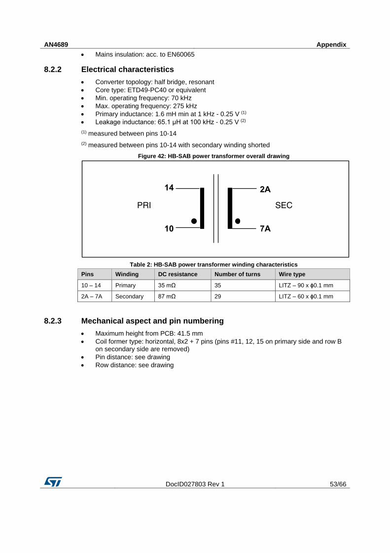
AN4689 Appendix
DocID027803 Rev 1 53/66
Mains insulation: acc. to EN60065
8.2.2 Electrical characteristics
Converter topology: half bridge, resonant
Core type: ETD49-PC40 or equivalent
Min. operating frequency: 70 kHz
Max. operating frequency: 275 kHz
Primary inductance: 1.6 mH min at 1 kHz - 0.25 V (1)
Leakage inductance: 65.1 μH at 100 kHz - 0.25 V (2)
(1) measured between pins 10-14
(2) measured between pins 10-14 with secondary winding shorted
Figure 42: HB-SAB power transformer overall drawing
Table 2: HB-SAB power transformer winding characteristics
Pins Winding DC resistance Number of turns Wire type
10 – 14 Primary 35 mΩ 35 LITZ – 90 x ɸ0.1 mm
2A – 7A Secondary 87 mΩ 29 LITZ – 60 x ɸ0.1 mm
8.2.3 Mechanical aspect and pin numbering
Maximum height from PCB: 41.5 mm
Coil former type: horizontal, 8x2 + 7 pins (pins #11, 12, 15 on primary side and row B on secondary side are removed)
Pin distance: see drawing
Row distance: see drawing
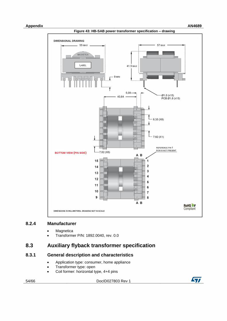
Appendix AN4689
54/66 DocID027803 Rev 1
Figure 43: HB-SAB power transformer specification – drawing
8.2.4 Manufacturer
Magnetica
Transformer P/N: 1892.0040, rev. 0.0
8.3 Auxiliary flyback transformer specification
8.3.1 General description and characteristics
Application type: consumer, home appliance
Transformer type: open
Coil former: horizontal type, 4+4 pins

AN4689 Appendix
DocID027803 Rev 1 55/66
Max. temp. rise: 45 ºC
Max. operating ambient temperature: 85 ºC
Mains insulation: acc. to EN60065
8.3.2 Electrical characteristics
Converter topology: flyback, CCM/DCM mode
Core type: E13/7/4 or equivalent
Typ. operating frequency: 115 kHz
Primary inductance: 3.9 mH ±20% at 1 kHz - 0.25 V (1)
Leakage inductance: 68 μH at 10 kHz - 0.25 V (2)
Saturation peak current: 0.17 A
Operating maximum peak current: 0.13 A
(1) measured between pins 1-2
(2) measured between pins 1-2 with pin 2-3-4-5-6-7-8 shorted
Figure 44: Auxiliary flyback transformer overall drawing
Table 3: Auxiliary flyback transformer winding characteristics
Pins Winding DC resistance Number of turns Wire type
1 – 2 Primary 6.44 Ω 212 G2 – ɸ0.10 mm
3 – 4 Auxiliary 454 mΩ 35 G2 – ɸ0.10 mm
5 – 6 Secondary 270 mΩ 18 Tex-E – ɸ0.2 mm
7 – 8 Secondary 267 mΩ 18 Tex-E – ɸ0.2 mm
8.3.3 Mechanical aspect and pin numbering
Maximum height from PCB: 15 mm
Coil former type: horizontal, 4+4 pins

Appendix AN4689
56/66 DocID027803 Rev 1
Pin distance: 3.81 mm
Row distance: 10.16 mm
Figure 45: Auxiliary flyback transformer specification – drawing

AN4689 Appendix
DocID027803 Rev 1 57/66
Figure 46: Auxiliary flyback transformer construction
8.3.4 Manufacturer
Magnetica
Transformer P/N: 1921.0049, rev. 0.1
8.4 Bill of materials
Table 4: Bill of materials
Item Reference Part type / part
value
Case style /
package Description Supplier
1 C1, C4, C9 2.2n - Y1 pitch 10mm
Ceramic Y1 capacitor - DE1E3KX222M
MURATA
2 C2, C3, C6, C7, C10, C11
680nF 18.1 x 7.5 x 12.1mm
Metallized polypropylene film capacitor - ECWF2W684JA
Panasonic
3 C5, C8 270μF 30 x 40mm
Aluminum electrolytic capacitor - EETHC2W271DA
Panasonic
4 C12, C16, C19 100μF 6.3 x 11mm
YXF - Miniature aluminum electrolytic capacitor - 20%
Rubycon
5 C13, C18 47μF 5 x 11mm
YXF - Miniature aluminum electrolytic capacitor - 20%
Rubycon
6 C14, C21, C22 470μF 10 x 16mm
YXF - Miniature aluminum electrolytic capacitor - 20%
Rubycon
7 C15 100nF 305VAC 13 x 6 x 12mm
Polypropylene film capacitors - 10%
AVX
8 C17 1000μF 24 x 45mm
Aluminum electrolytic capacitor - B43508A2108M000
EPCOS
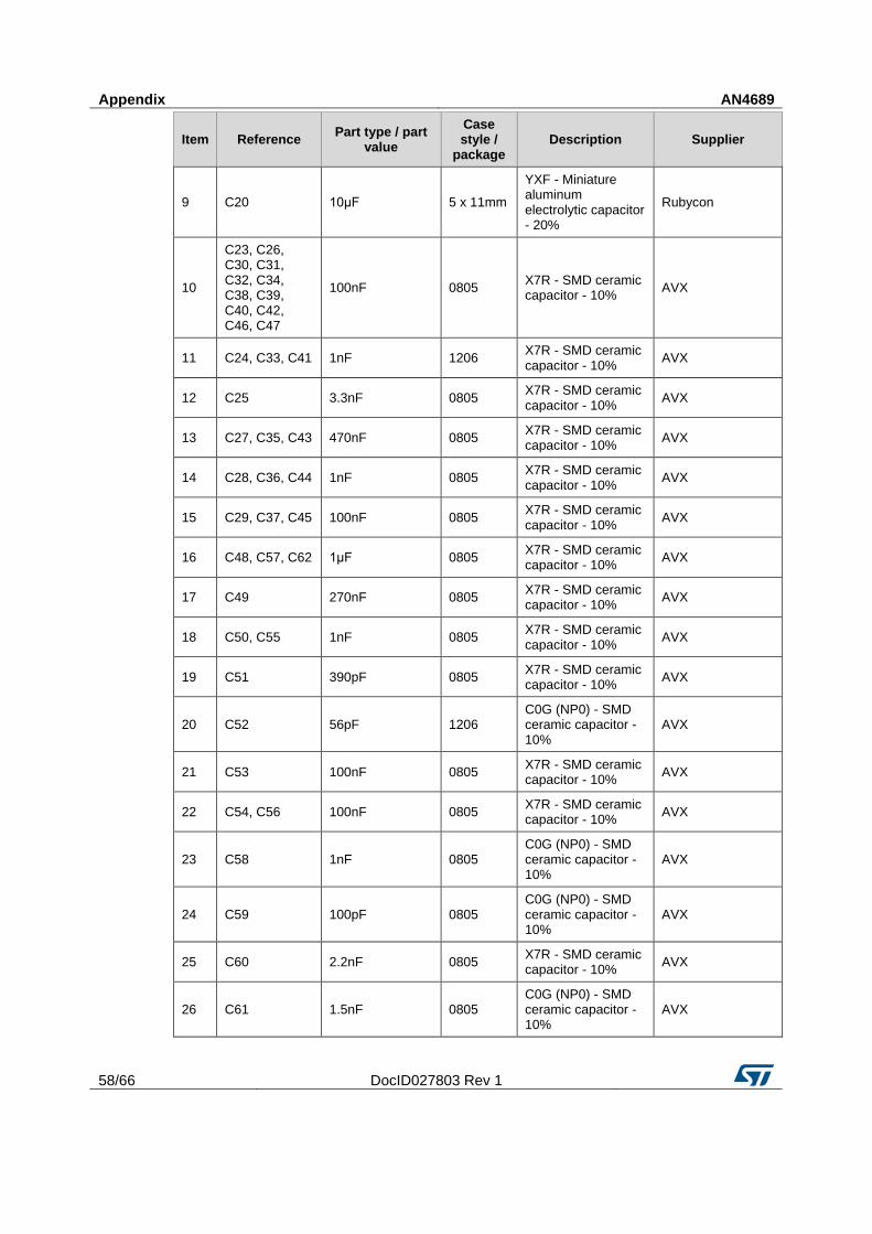
Appendix AN4689
58/66 DocID027803 Rev 1
Item Reference Part type / part
value
Case style /
package Description Supplier
9 C20 10μF 5 x 11mm
YXF - Miniature aluminum electrolytic capacitor - 20%
Rubycon
10
C23, C26, C30, C31, C32, C34, C38, C39, C40, C42, C46, C47
100nF 0805 X7R - SMD ceramic capacitor - 10%
AVX
11 C24, C33, C41 1nF 1206 X7R - SMD ceramic capacitor - 10%
AVX
12 C25 3.3nF 0805 X7R - SMD ceramic capacitor - 10%
AVX
13 C27, C35, C43 470nF 0805 X7R - SMD ceramic capacitor - 10%
AVX
14 C28, C36, C44 1nF 0805 X7R - SMD ceramic capacitor - 10%
AVX
15 C29, C37, C45 100nF 0805 X7R - SMD ceramic capacitor - 10%
AVX
16 C48, C57, C62 1μF 0805 X7R - SMD ceramic capacitor - 10%
AVX
17 C49 270nF 0805 X7R - SMD ceramic capacitor - 10%
AVX
18 C50, C55 1nF 0805 X7R - SMD ceramic capacitor - 10%
AVX
19 C51 390pF 0805 X7R - SMD ceramic capacitor - 10%
AVX
20 C52 56pF 1206 C0G (NP0) - SMD ceramic capacitor - 10%
AVX
21 C53 100nF 0805 X7R - SMD ceramic capacitor - 10%
AVX
22 C54, C56 100nF 0805 X7R - SMD ceramic capacitor - 10%
AVX
23 C58 1nF 0805 C0G (NP0) - SMD ceramic capacitor - 10%
AVX
24 C59 100pF 0805 C0G (NP0) - SMD ceramic capacitor - 10%
AVX
25 C60 2.2nF 0805 X7R - SMD ceramic capacitor - 10%
AVX
26 C61 1.5nF 0805 C0G (NP0) - SMD ceramic capacitor - 10%
AVX

AN4689 Appendix
DocID027803 Rev 1 59/66
Item Reference Part type / part
value
Case style /
package Description Supplier
27 C63 100nF 0805 X7R - SMD ceramic capacitor - 10%
AVX
28 C64 33nF 0805 X7R - SMD ceramic capacitor - 10%
AVX
29 C65 3.3nF 0805 C0G (NP0) - SMD ceramic capacitor - 10%
AVX
30 C66 22nF 0805 C0G (NP0) - SMD ceramic capacitor - 10%
AVX
31 D1, D2, D3, D4, D7
Green T-1 (3mm)
TH green LED - HLMP-Y802-F0000
AVAGO TECHNOLOGIES
32 D5 PKC-136 DO-15 Peak clamp STMicroelectronics
33 D6, D8 Red T-1 (3mm)
TH red LED - HLMP-Y651-G0000
AVAGO TECHNOLOGIES
34
D9, D10, D14, D15, D17, D18, D21, D22, D25, D26, D28, D29
STPS20200CG D2PAK High voltage power Schottky rectifier
STMicroelectronics
35
D11, D12, D16, D19, D23, D24, D31, D33
1N4148WS SOD-323 SMD diode
36 D13, D20, D27 STTH1L06A SMA SMD Turbo 2 ultrafast high voltage rectifier
STMicroelectronics
37 D30, D32, D34 STTH102A SMA SMD high efficiency ultrafast diode
STMicroelectronics
38 D35 BAT20J SOD-323 SMD ultra low leakage current Schottky diode
STMicroelectronics
39 D36 B-15 MiniMELF Zener diode - TZMB15 - 2%
VISHAY
40 HS1, HS2, HS3
0S515-50B 50 x 30 x 45mm
Heat sink AAVID THERMALLOY
41 ISO1, ISO2 SFH618A-3 DIP-4 Optocoupler, single channel
VISHAY
42 J1 HVIN 5 pin HV DC input connector - 26-60-4050
MOLEX
43 J2 VDC 5 pin LV primary DC connector - 1729157
PHOENIX CONTACT

Appendix AN4689
60/66 DocID027803 Rev 1
Item Reference Part type / part
value
Case style /
package Description Supplier
44 J3 OUT 3 pin
Output voltage screw connector - MSTBVA2,5/3-G-5,08 and MSTB2,5/3-ST-5,08
PHOENIX CONTACT
45 J4 CON50A 2 x 25pin - male
50 pins connector
46 L1, L4, L5 10μF 1008 SMD inductor - ELJPC100KF - 10%
ELJPC100KF
47 L2, L3 33μF 1812 SMD inductor - B82432T1333K000 - 10%
EPCOS
48 Q1, Q2, Q3, Q4, Q5, Q6
STF21N65M5 TO-220FP
MDmesh V power MOSFET
STMicroelectronics
49 Q7, Q9, Q11, Q13, Q15, Q17
PBSS4041PT SOT-23 SMD PNP general purpose amplifier
50 Q8, Q10, Q12, Q14, Q16, Q18
PBSS4041NT SOT-23 SMD NPN general purpose amplifier
51 Q19 STN3PF06 SOT223 P-channel power Mosfet
STMicroelectronics
52 Q20, Q22, Q23, Q25, Q26
BC847C SOT23 General purpose NPN
53 Q21, Q24 BC857C SOT23 General purpose PNP
54 RS_1, RS_2, RS_3
20mΩ 1206 SMD resistor - 1% BC COMPONENTS
55 R1, R11, R16, R25, R30, R40, R119
0R0 0805 SMD resistor - 5% BC COMPONENTS
56 R2, R13, R17, R27, R31, R42
1kΩ 0805 SMD resistor - 5% BC COMPONENTS
57 R3, R14, R20, R28, R34, R43
2.2R 0805 SMD resistor - 5% BC COMPONENTS
58
R4, R12, R18, R26, R32, R35, R41, R51, R56, R70, R71
100kΩ 0805 SMD resistor - 5% BC COMPONENTS
59 R5, R15, R19, R29, R33, R44
20R 0805 SMD resistor - 5% BC COMPONENTS
60 R6, R9, R21, R23, R36, R38
10R 1206 SMD resistor - 5% BC COMPONENTS
61 R7 15kΩ 0805 SMD resistor - 5% BC COMPONENTS
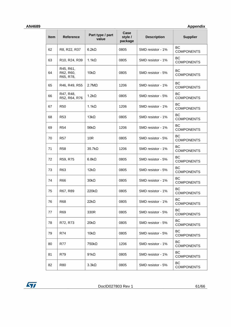
AN4689 Appendix
DocID027803 Rev 1 61/66
Item Reference Part type / part
value
Case style /
package Description Supplier
62 R8, R22, R37 6.2kΩ 0805 SMD resistor - 1% BC COMPONENTS
63 R10, R24, R39 1.1kΩ 0805 SMD resistor - 1% BC COMPONENTS
64 R45, R61, R62, R60, R65, R78,
10kΩ 0805 SMD resistor - 5% BC COMPONENTS
65 R46, R49, R55 2.7MΩ 1206 SMD resistor - 1% BC COMPONENTS
66 R47, R48, R52, R64, R76
1.2kΩ 0805 SMD resistor - 5% BC COMPONENTS
67 R50 1.1kΩ 1206 SMD resistor - 1% BC COMPONENTS
68 R53 13kΩ 0805 SMD resistor - 1% BC COMPONENTS
69 R54 56kΩ 1206 SMD resistor - 1% BC COMPONENTS
70 R57 10R 0805 SMD resistor - 5% BC COMPONENTS
71 R58 35.7kΩ 1206 SMD resistor - 1% BC COMPONENTS
72 R59, R75 6.8kΩ 0805 SMD resistor - 5% BC COMPONENTS
73 R63 12kΩ 0805 SMD resistor - 5% BC COMPONENTS
74 R66 30kΩ 0805 SMD resistor - 1% BC COMPONENTS
75 R67, R89 220kΩ 0805 SMD resistor - 1% BC COMPONENTS
76 R68 22kΩ 0805 SMD resistor - 1% BC COMPONENTS
77 R69 330R 0805 SMD resistor - 5% BC COMPONENTS
78 R72, R73 20kΩ 0805 SMD resistor - 5% BC COMPONENTS
79 R74 10kΩ 0805 SMD resistor - 5% BC COMPONENTS
80 R77 750kΩ 1206 SMD resistor - 1% BC COMPONENTS
81 R79 91kΩ 0805 SMD resistor - 1% BC COMPONENTS
82 R80 3.3kΩ 0805 SMD resistor - 5% BC COMPONENTS

Appendix AN4689
62/66 DocID027803 Rev 1
Item Reference Part type / part
value
Case style /
package Description Supplier
83 R81 2.2kΩ 0805 SMD resistor - 1% BC COMPONENTS
84 R82, R86 360kΩ 1206 SMD resistor - 1% BC COMPONENTS
85 R83 2.7kΩ 0805 SMD resistor - 5% BC COMPONENTS
86 R84 3kΩ 0805 SMD resistor - 5% BC COMPONENTS
87 R85 3.6kΩ 0805 SMD resistor - 5% BC COMPONENTS
88 R87 18kΩ 0805 SMD resistor - 1% BC COMPONENTS
89 R88 15kΩ 0805 SMD resistor - 1% BC COMPONENTS
90 R90 1MΩ 0805 SMD resistor - 1% BC COMPONENTS
91 T1, T3, T5 n.m. ETD44 HB transformer Magnetica
92 T2, T4, T6 1892.0040 ETD49 HB transformer Magnetica
93 T7 1921.0049 E13 AUX supply transformer
Magnetica
94 U1, U2, U3 L6391 SO-14 High-voltage high and low side driver
STMicroelectronics
95 U4 LD1086D2T33TR D2PAK 3V3 linear regulator STMicroelectronics
96 U5 VIPER06HS SSO10 Fixed frequency Viper 4W high voltage converter
STMicroelectronics
97 U6 TSX561A SOT23-5 Single op-amp STMicroelectronics
98 U7 TSM1013A MiniSO-8 Constant voltage and constant current controller
STMicroelectronics
99 C201, C202 n.m. 0603 C0G (NP0) - SMD ceramic capacitor
AVX
100 C203, C204, C210
1μF 0603 Y5V - SMD ceramic capacitor - 10%
AVX
101 C205, C206, C207, C208
100nF 0603 X7R - SMD ceramic capacitor - 10%
AVX
102 C209 10nF 0603 X7R - SMD ceramic capacitor - 10%
AVX
103 C211, C212, C213, C214, C215
100pF 0603 C0G (NP0) - SMD ceramic capacitor - 10%
AVX

AN4689 Appendix
DocID027803 Rev 1 63/66
Item Reference Part type / part
value
Case style /
package Description Supplier
104
C216, C217, C218, C219, C220, C221, C222, C223
100pF 0603 X7R - SMD ceramic capacitor - 10%
AVX
105 J201 DC in 2 pin WAGO connector
106 J202 CON50A 2 x 25 pin - female
50 pin connector
107 J203 SWIM I/F 4 pin PCB header single row
108 J204 UART I/F 3.5mm jack connector
109 J205 PIN_STRIP_10 10 pin PCB header single row
110 J206 PIN_STRIP_9 9 pin PCB header single row
111 J207 PIN_STRIP_4 4 pin PCB header single row
112 J208 PIN_STRIP_5 5 pin PCB header single row
113 J209 PIN_STRIP_10 10 pin PCB header single row
114 L201 WE-CBF 0603 SMD EMI suppression ferrite bead - 74279262
WE
115 P201 RESET Push button

Appendix AN4689
64/66 DocID027803 Rev 1
Item Reference Part type / part
value
Case style /
package Description Supplier
116
R201, R202, R203, R204, R205, R206, R207, R208, R209, R210, R211, R212, R213, R214, R215, R216, R217, R218, R219, R220, R221, R222, R223, R224, R225, R226, R227, R228, R229, R230, R231, R232, R233, R234, R235, R236, R237, R238, R239, R240, R241, R242, R243, R244, R245, R246, R247, R248, R249, R250, R251, R252, R256, R257, R259, R269, R270
0R 0603 SMD resistor - 5% BC COMPONENTS
118
R253, R254, R255, R258, R260, R261, R262, R263, R264, R265, R266, R267, R268
100R 0603 SMD resistor - 5% BC COMPONENTS
119 U201 STNRG388A TSSOP38 STNRG388A STMicroelectronics
120 X201 n.m. XTAL 16MHz

AN4689 Revision history
DocID027803 Rev 1 65/66
9 Revision history Table 5: Document revision history
Date Version Changes
23-Sep-2015 1 Initial release.

AN4689
66/66 DocID027803 Rev 1
IMPORTANT NOTICE – PLEASE READ CAREFULLY
STMicroelectronics NV and its subsidiaries (“ST”) reserve the right to make changes, corrections, enhancements, modifications , and improvements to ST products and/or to this document at any time without notice. Purchasers should obtain the latest relevant information on ST products before placing orders. ST products are sold pursuant to ST’s terms and conditions of sale in place at the time of order acknowledgement.
Purchasers are solely responsible for the choice, selection, and use of ST products and ST assumes no liability for application assistance or the design of Purchasers’ products.
No license, express or implied, to any intellectual property right is granted by ST herein.
Resale of ST products with provisions different from the information set forth herein shall void any warranty granted by ST for such product.
ST and the ST logo are trademarks of ST. All other product or service names are the property of their respective owners.
Information in this document supersedes and replaces information previously supplied in any prior versions of this document.
© 2015 STMicroelectronics – All rights reserved