EVALUATION KIT AVAILABLE +3.3V, 2.5Gbps SDH… · for SDH/SONET applications up to 2.5Gbps. The...
15
General Description The MAX3869 is a complete, single +3.3V laser driver for SDH/SONET applications up to 2.5Gbps. The device accepts differential PECL data and clock inputs and provides bias and modulation currents for driving a laser. A synchronizing input latch can be used (if a clock signal is available) to reduce jitter. An automatic power control (APC) feedback loop is incorporated to maintain a constant average optical power over temperature and lifetime. The wide modula- tion current range of 5mA to 60mA and bias current of 1mA to 100mA are easy to program, making this prod- uct ideal for use in various SDH/SONET applications. The MAX3869 also provides enable control, two current monitors that are directly proportional to the laser bias and modulation currents, and a failure-monitor output to indi- cate when the APC loop is unable to maintain the average optical power. The MAX3869 is available in 32-pin TQFP and small 32-pin QFN packages as well as dice. Applications SONET/SDH Transmission Systems Add/Drop Multiplexers Digital Cross-Connects Section Regenerators 2.5Gbps Optical Transmitters Features ♦ Single +3.3V or +5V Power Supply ♦ 64mA Supply Current at +3.3V ♦ Programmable Bias Current from 1mA to 100mA ♦ Programmable Modulation Current from 5mA to 60mA ♦ Bias Current and Modulation Current Monitors ♦ 87ps Rise/Fall Time ♦ Automatic Average Power Control with Failure Monitor ♦ Complies with ANSI, ITU, and Bellcore SDH/SONET Specifications ♦ Enable Control *Exposed pad. **Package Code: G3255-1 ***Dice are designed to operate over this range, but are tested and guaranteed at T A = +25°C only. Contact factory for availability. +Denotes lead-free package. Ordering Information MAX3869 +3.3V, 2.5Gbps SDH/SONET Laser Driver with Current Monitors and APC ________________________________________________________________ Maxim Integrated Products 1 EVALUATION KIT AVAILABLE 124Ω 124Ω SERIALIZER WITH CLOCK GEN. 124Ω 23Ω LD 25Ω +3.3V +3.3V 0.056µF 0.01µF BIASMON MODMON +3.3V 1000pF BIASMAX LATCH ENABLE FAIL MODSET APCSET APCFILT CLK- CLK+ DATA- DATA+ FERRITE BEAD OUT+ BIAS MD OUT- CAPC 124Ω 84.5Ω 84.5Ω 84.5Ω 84.5Ω MAX3869 MAX3890 Typical Application Circuit 19-1570; Rev 4; 1/05 Pin Configuration appears at end of data sheet. For pricing, delivery, and ordering information, please contact Maxim/Dallas Direct! at 1-888-629-4642, or visit Maxim’s website at www.maxim-ic.com. PART TEMP RANGE PIN-PACKAGE MAX3869EHJ -40°C to +85°C 32 TQFP-EP* MAX3869EHJ+ -40°C to +85°C 32 TQFP-EP* MAX3869EGJ -40°C to +85°C 32 QFN** MAX3869E/D -40°C to +85°C Dice***
Transcript of EVALUATION KIT AVAILABLE +3.3V, 2.5Gbps SDH… · for SDH/SONET applications up to 2.5Gbps. The...
General DescriptionThe MAX3869 is a complete, single +3.3V laser driverfor SDH/SONET applications up to 2.5Gbps. Thedevice accepts differential PECL data and clock inputsand provides bias and modulation currents for driving alaser. A synchronizing input latch can be used (if aclock signal is available) to reduce jitter.
An automatic power control (APC) feedback loop isincorporated to maintain a constant average opticalpower over temperature and lifetime. The wide modula-tion current range of 5mA to 60mA and bias current of1mA to 100mA are easy to program, making this prod-uct ideal for use in various SDH/SONET applications.
The MAX3869 also provides enable control, two currentmonitors that are directly proportional to the laser bias andmodulation currents, and a failure-monitor output to indi-cate when the APC loop is unable to maintain the averageoptical power. The MAX3869 is available in 32-pin TQFPand small 32-pin QFN packages as well as dice.
ApplicationsSONET/SDH Transmission Systems
Add/Drop Multiplexers
Digital Cross-Connects
Section Regenerators
2.5Gbps Optical Transmitters
Features♦ Single +3.3V or +5V Power Supply
♦ 64mA Supply Current at +3.3V
♦ Programmable Bias Current from 1mA to 100mA
♦ Programmable Modulation Current from 5mA to 60mA
♦ Bias Current and Modulation Current Monitors
♦ 87ps Rise/Fall Time
♦ Automatic Average Power Control with FailureMonitor
♦ Complies with ANSI, ITU, and BellcoreSDH/SONET Specifications
♦ Enable Control
*Exposed pad.**Package Code: G3255-1***Dice are designed to operate over this range, but are tested andguaranteed at TA = +25°C only. Contact factory for availability.+Denotes lead-free package.
Ordering Information
MA
X3
86
9
+3.3V, 2.5Gbps SDH/SONET Laser Driver with Current Monitors and APC
________________________________________________________________ Maxim Integrated Products 1
EVALUATION KIT
AVAILABLE
124Ω 124Ω
SERIALIZERWITH
CLOCK GEN.
124Ω
23Ω
LD25Ω
+3.3V+3.3V
0.056µF
0.01µF
BIASMON
MODMON
+3.3V
1000pF
BIAS
MAX
LATC
H
ENAB
LE
FAIL
MOD
SET
APCS
ET
APCF
ILT
CLK-
CLK+
DATA-
DATA+
FERRITEBEAD
OUT+
BIAS
MD
OUT-
CAPC
124Ω
84.5Ω 84.5Ω 84.5Ω84.5Ω
MAX3869
MAX3890
Typical Application Circuit
19-1570; Rev 4; 1/05
Pin Configuration appears at end of data sheet.
For pricing, delivery, and ordering information, please contact Maxim/Dallas Direct! at 1-888-629-4642, or visit Maxim’s website at www.maxim-ic.com.
PART TEMP RANGE PIN-PACKAGE
MAX3869EHJ -40°C to +85°C 32 TQFP-EP*
MAX3869EHJ+ -40°C to +85°C 32 TQFP-EP*
MAX3869EGJ -40°C to +85°C 32 QFN**
MAX3869E/D -40°C to +85°C Dice***
MA
X3
86
9
+3.3V, 2.5Gbps SDH/SONET Laser Driver with Current Monitors and APC
2 _______________________________________________________________________________________
IMD = 1mA
IMD = 18µA 90
ENABLE = low (Note 4)
APC open loop
(Note 3)
900
(Note 2)
(Note 5)
Sourcing 50µA
ENABLE, LATCH
(Note 6)
ENABLE, LATCH
IBIAS = 100mA
APC open loop
Figure 1
PECL compatible
Sinking 100µA
CONDITIONS
%-15 15Monitor-Diode Bias AbsoluteAccuracy
ppm/°C-480 50 480Monitor-Diode Bias Setpoint
Stability
µA18 1000IMDMonitor-Diode DC Current Range
V1.5Monitor-Diode Reverse BiasVoltage
V0.1 0.44TTL Output Low Voltage FAIL
µA100IBIAS-OFFBias Off-Current
mA1 100IBIAS
mA64 112ICCSupply Current
Bias Current Range
V 2.4 VCC - 0.3 VCCTTL Output High Voltage FAIL
V0.8TTL Input Low Voltage
V2.0TTL Input High Voltage
µA-1 10IINClock and Data Input Current
ppm/°C230
Bias-Current Stability
%-15 15(Note 5)Bias-Current Absolute Accuracy
mVp-p200 1600VIDDifferential Input Voltage
VVCC - VCC - VCC -1.49 1.32 VID/4
VICMCommon-Mode Input Voltage
UNITSMIN TYP MAXSYMBOLPARAMETER
DC ELECTRICAL CHARACTERISTICS(VCC = +3.14V to +5.5V, TA = -40°C to +85°C. Typical values are at VCC = +3.3V, IMOD = 30mA, IBIAS = 60mA, TA = +25°C, unlessotherwise noted.) (Note 1)
Stresses beyond those listed under “Absolute Maximum Ratings” may cause permanent damage to the device. These are stress ratings only, and functionaloperation of the device at these or any other conditions beyond those indicated in the operational sections of the specifications is not implied. Exposure toabsolute maximum rating conditions for extended periods may affect device reliability.
Supply Voltage, VCC............................................. -0.5V to +7.0VCurrent into BIAS ...........................................-20mA to +150mACurrent into OUT+, OUT- ................................-20mA to +100mACurrent into MD.....................................................-5mA to +5mAVoltage at DATA+, DATA-, CLK+, CLK-, ENABLE,
LATCH, FAIL, BIASMON, MODMON .....-0.5V to (VCC + 0.5V)Voltage at APCFILT, CAPC, MODSET,
BIASMAX, APCSET ...........................................-0.5V to +3.0VVoltage at OUT+, OUT-.............................+1.5V to (VCC + 1.5V)
Voltage at BIAS .........................................+1.0V to (VCC + 0.5V)Continuous Power Dissipation (TA = +85°C)
32-Pin TQFP-EP (derate 22.2mW/°C above +85°C) ..1444mW32-Pin QFN (derate 20.84mW/°C above +85°C) .......1667mW
Storage Temperature Range .............................-65°C to +165°COperating Junction Temperature Range...........-55°C to +150°CProcessing Temperature (die) .........................................+400°CLead Temperature (soldering, 10s) .................................+300°C
ABSOLUTE MAXIMUM RATINGS
IBIAS/IBIASMON A/A37ABIASBIASMON to IBIAS Gain
IMOD/IMODMON A/A29AMODMODMON to IMOD Gain
IBIAS = 1mA
MA
X3
86
9
+3.3V, 2.5Gbps SDH/SONET Laser Driver with Current Monitors and APC
_______________________________________________________________________________________ 3
AC ELECTRICAL CHARACTERISTICS(VCC = +3.14V to +5.5V, load as shown in Figure 2, TA = -40°C to +85°C. Typical values are at VCC = +3.3V, IMOD = 30mA, TA = +25°C.)(Note 7)
Note 1: Dice are tested at TA = +25°C only.Note 2: Tested at RMODSET = 2.49kΩ, RBIASMAX = 1.69kΩ, excluding IBIAS and IMOD.Note 3: Voltage on BIAS pin is (VCC - 1.6V).Note 4: Both the bias and modulation currents will be switched off if any of the current set pins are grounded.Note 5: Accuracy refers to part-to-part variation.Note 6: Assuming that the laser to monitor-diode transfer function does not change with temperature. Guaranteed by design and
characterization.Note 7: AC characteristics are guaranteed by design and characterization.Note 8: Measured with 622Mbps 0-1 pattern, LATCH = high.Note 9: PWD = (wider pulse - narrower pulse) / 2.Note 10: See Typical Operating Characteristics for worst-case distribution.
IMOD = 5mA 300
78
LATCH = high, Figure 3
LATCH = high, Figure 3
20% to 80% (Note 8)
ps
69
(Note 8)
20% to 80% (Note 8)
ENABLE = low (Note 4)
IMOD = 60mA
(Note 5)
Jitter BW = 12kHz to 20MHz, 0-1 pattern
(Notes 8, 9)
CONDITIONS
tROutput Rise-Time ps
psp-p7 20Jitter Generation
ps14 50PWDPulse-Width Distortion
mA5 60IMODModulation-Current Range
ps100tH
ps100tSUInput Latch Setup Time
Input Latch Hold Time
bits80Maximum Consecutive IdenticalDigits
ns250Enable and Start-Up Delay
%±15Output Aberrations
79tFOutput Fall- Time
µA200IMOD-OFFModulation-Off Current
ppm/°C-480 -8 480
Modulation-Current Stability
%-15 15Modulation-Current AbsoluteAccuracy
87 (Note 10)
UNITSMIN TYP MAXSYMBOLPARAMETER
MAX3869EHJ
MAX3869E/D
MAX3869EHJ
MAX3869E/D
DATA+
DATA-
(DATA+) - (DATA-)
IOUT+
100mV MIN
800mV MAX
200mVp-p MIN
1600mVp-p MAX
IMOD
Figure 1. Required Input Signal and Output Polarity
MA
X3
86
9
+3.3V, 2.5Gbps SDH/SONET Laser Driver with Current Monitors and APC
4 _______________________________________________________________________________________
CLK
DATA
tCLK = 402ps
tSU tH
Figure 3. Setup/Hold Time Definition
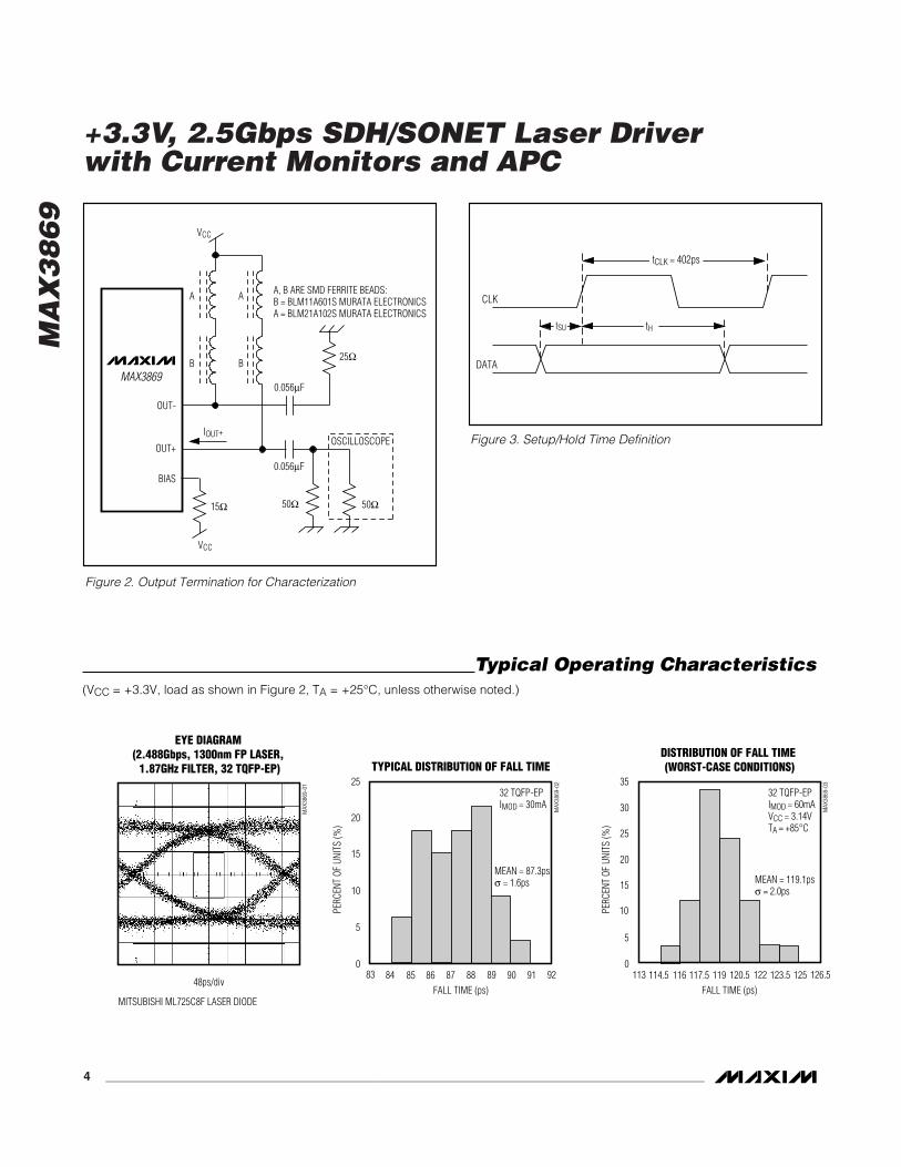
0.056µF
OUT+
BIAS
OUT-
A
B
A A, B ARE SMD FERRITE BEADS:B = BLM11A601S MURATA ELECTRONICSA = BLM21A102S MURATA ELECTRONICS
B
VCC
50Ω15Ω
OSCILLOSCOPE
50Ω
25Ω
0.056µF
VCC
MAX3869
IOUT+
Figure 2. Output Termination for Characterization
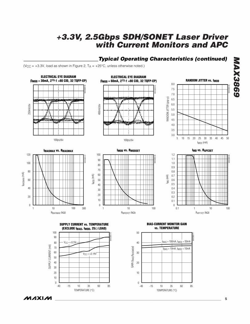
Typical Operating Characteristics (VCC = +3.3V, load as shown in Figure 2, TA = +25°C, unless otherwise noted.)
EYE DIAGRAM(2.488Gbps, 1300nm FP LASER, 1.87GHz FILTER, 32 TQFP-EP)
MAX
3869
-01
48ps/div
MITSUBISHI ML725C8F LASER DIODE
0
5
15
10
20
25
8483 87
32 TQFP-EPIMOD = 30mA
MEAN = 87.3psσ = 1.6ps
88 90898685 91 92
TYPICAL DISTRIBUTION OF FALL TIME
MAX
3869
-02
FALL TIME (ps)
PERC
ENT
OF U
NITS
(%)
0
5
20
15
10
30
25
35
114.5113 119
32 TQFP-EPIMOD = 60mAVCC = 3.14VTA = +85°C
MEAN = 119.1psσ = 2.0ps
120.5 123.5122117.5116 125 126.5
DISTRIBUTION OF FALL TIME (WORST-CASE CONDITIONS)
MAX
3869
-03
FALL TIME (ps)
PERC
ENT
OF U
NITS
(%)
MA
X3
86
9
+3.3V, 2.5Gbps SDH/SONET Laser Driver with Current Monitors and APC
_______________________________________________________________________________________ 5
120
01 10 100 300
IBIASMAX vs. RBIASMAX
MAX
3869
-07
RBIASMAX (kΩ)
I BIA
SMAX
(mA)
40
80
100
20
60
1.2
00.1 1 10 100
IMD vs. RAPCSET
0.4
MAX
3869
-09
RAPCSET (kΩ)
I MD
(mA)
0.6
0.8
1.01.1
0.30.20.1
0.5
0.7
0.9
100
01 10 100
IMOD vs. RMODSET
20
10
MAX
3869
-08
RMODSET (kΩ)
I MOD
(mA)
40
30
60
70
50
80
90
0
10
60
50
40
30
20
90
70
80
100
-40 -15 10 35 60 85
SUPPLY CURRENT vs. TEMPERATURE(EXCLUDE IBIAS, IMOD, 25Ω LOAD)
MAX
3869
-10
TEMPERATURE (°C)
SUPP
LY C
URRE
NT (m
A)
VCC = +5.5V
VCC = +3.14V
0
10
30
20
40
50
-40 -15 10 35 60 85
BIAS-CURRENT MONITOR GAINvs. TEMPERATURE
MAX
3869
-11
TEMPERATURE (°C)
GAIN
(IBI
AS/I B
IASM
ON)
IBIAS = 100mA, IMOD = 50mA
IBIAS = 10mA, IMOD = 10mA
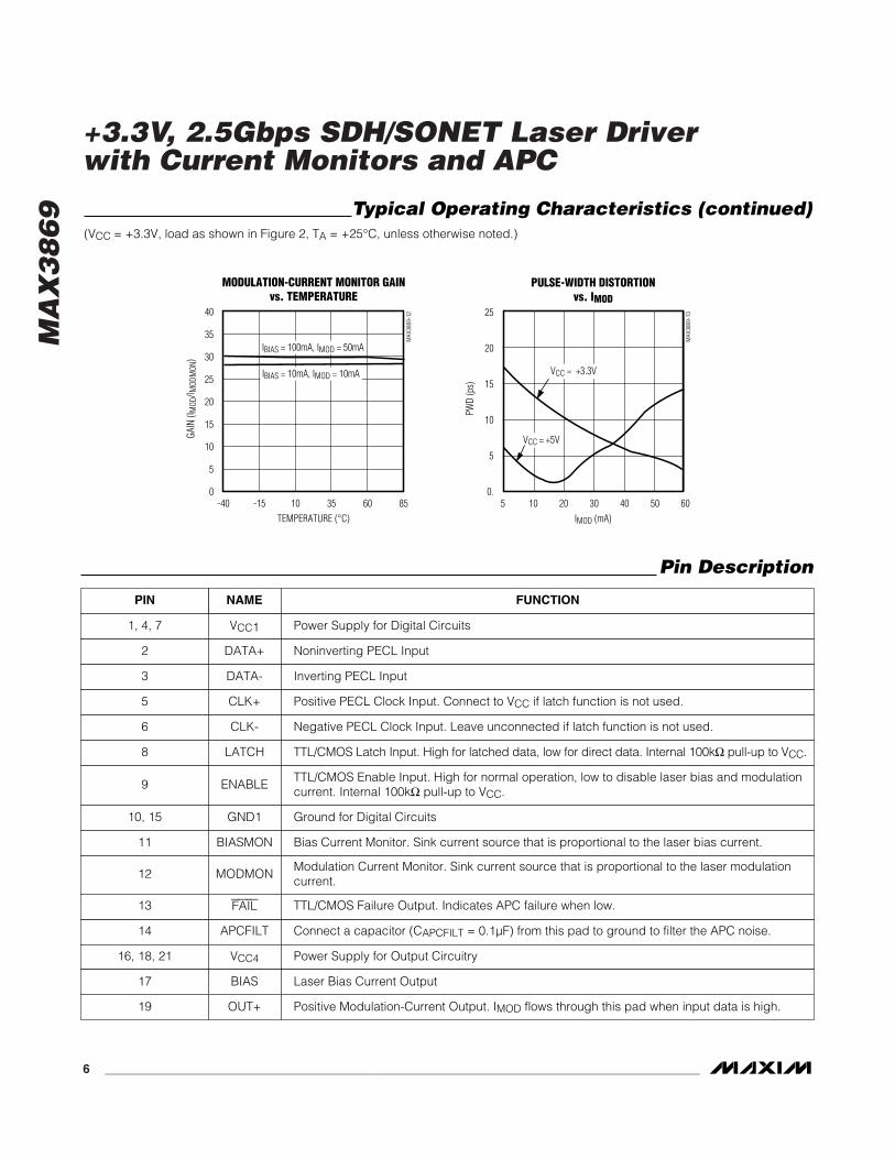
ELECTRICAL EYE DIAGRAM(IMOD = 30mA, 213-1 +80 CID, 32 TQFP-EP)
MAX
3869
-04
100ps/div
250m
V/di
v
ELECTRICAL EYE DIAGRAM(IMOD = 60mA, 213-1 +80 CID, 32 TQFP-EP)
MAX
3869
-05
100ps/div
400m
V/di
v
3.0
4.0
3.5
5.0
4.5
6.0
5.5
6.5
7.5
7.0
8.0
5 15 20 2510 30 35 40 45 50
RANDOM JITTER vs. IMOD
MAX
3869
-06
IMOD (mA)
RAND
OM JI
TTER
(psp
-p)
Typical Operating Characteristics (continued)(VCC = +3.3V, load as shown in Figure 2, TA = +25°C, unless otherwise noted.)
MA
X3
86
9
+3.3V, 2.5Gbps SDH/SONET Laser Driver with Current Monitors and APC
6 _______________________________________________________________________________________
Pin Description
Typical Operating Characteristics (continued)(VCC = +3.3V, load as shown in Figure 2, TA = +25°C, unless otherwise noted.)
NAME FUNCTION
1, 4, 7 VCC1 Power Supply for Digital Circuits
2 DATA+ Noninverting PECL Input
PIN
3 DATA- Inverting PECL Input
8 LATCH TTL/CMOS Latch Input. High for latched data, low for direct data. Internal 100kΩ pull-up to VCC.
6 CLK- Negative PECL Clock Input. Leave unconnected if latch function is not used.
5 CLK+ Positive PECL Clock Input. Connect to VCC if latch function is not used.
14 APCFILT Connect a capacitor (CAPCFILT = 0.1µF) from this pad to ground to filter the APC noise.
12 MODMONModulation Current Monitor. Sink current source that is proportional to the laser modulationcurrent.
11 BIASMON Bias Current Monitor. Sink current source that is proportional to the laser bias current.
10, 15 GND1 Ground for Digital Circuits
9 ENABLETTL/CMOS Enable Input. High for normal operation, low to disable laser bias and modulationcurrent. Internal 100kΩ pull-up to VCC.
19 OUT+ Positive Modulation-Current Output. IMOD flows through this pad when input data is high.
16, 18, 21 VCC4 Power Supply for Output Circuitry
17 BIAS Laser Bias Current Output
13 FAIL TTL/CMOS Failure Output. Indicates APC failure when low.
0.
5
15
10
20
25
5 2010 30 40 50 60
PULSE-WIDTH DISTORTIONvs. IMOD
MAX
3869
-13
IMOD (mA)
PWD
(ps)
VCC = +5V
VCC = +3.3V
0
5
10
15
20
25
30
35
40
-40 -15 10 35 60 85
MODULATION-CURRENT MONITOR GAINvs. TEMPERATURE
MAX
3869
-12
TEMPERATURE (°C)
GAIN
(IM
OD/I M
ODM
ON)
IBIAS = 100mA, IMOD = 50mA
IBIAS = 10mA, IMOD = 10mA
_______________Detailed DescriptionThe MAX3869 laser driver consists of two main parts: ahigh-speed modulation driver and a laser-biasing blockwith automatic power control (APC). The circuit designis optimized for both high-speed and low-voltage(+3.3V) operation. To minimize the pattern-dependentjitter of the input signal at speeds as high as 2.5Gbps,the device accepts a differential PECL clock signal fordata retiming. When LATCH is high, the input data issynchronized by the clock signal. When LATCH is low,the input data is directly applied to the output stage.
The output stage is composed of a high-speed differentialpair and a programmable modulation current source.Since the modulation output drives a maximum currentof 60mA into the laser with an edge speed of 100ps,large transient voltage spikes can be generated (due tothe parasitic inductance). These transients and thelaser forward voltage leave insufficient headroom forthe proper operation of the laser driver if the modulationoutput is DC-coupled to the laser diode. To solve thisproblem, the MAX3869’s modulation output is designedto be AC-coupled to the cathode of a laser diode. Anexternal pull-up inductor is necessary to DC-bias themodulation output at VCC. Such a configuration isolateslaser forward voltage from the output circuitry and
allows the output at OUT+ to swing above and belowthe supply voltage VCC. A simplified functional diagramis shown in Figure 4.
The MAX3869 modulation output is optimized for driv-ing a 25Ω load; the minimum required voltage at OUT+is 2.0V. Modulation current swings of 80mA are possi-ble, but due to minimum power-supply and jitterrequirements at 2.5Gbps, the specified maximum mod-ulation current is limited to 60mA. To interface with thelaser diode, a damping resistor (RD) is required forimpedance matching. An RC shunt network may alsobe necessary to compensate for the laser-diode para-sitic inductance, thereby improving the optical outputaberrations and duty-cycle distortion.
At the data rate of 2.5Gbps, any capacitive load at thecathode of a laser diode will degrade the optical outputperformance. Since the BIAS output is directly connect-ed to the laser cathode, minimize the parasitic capaci-tance associated with this pin by using an inductor toisolate the BIAS pin from the laser cathode.
Automatic Power Control To maintain constant average optical power, theMAX3869 incorporates an APC loop to compensate forthe changes in laser threshold current over temperatureand lifetime. A back-facet photodiode mounted in the
MA
X3
86
9
+3.3V, 2.5Gbps SDH/SONET Laser Driver with Current Monitors and APC
_______________________________________________________________________________________ 7
NAME FUNCTIONPIN
25 VCC3 Power Supply for APC
24 MDMonitor Diode Input. Connect this pad to a monitor photodiode anode. A capacitor to groundis required to filter high-speed AC monitor photocurrent.
20 OUT- Negative Modulation-Current Output. IMOD flows through this pad when input data is low.
32 VCC2 Power Supply for Internal Reference
31 BIASMAXA resistor connected from this pad to ground sets the maximum bias current. The APC function can subtract from this maximum value, but cannot add to it.
30 MODSET A resistor connected from this pad to ground sets the desired modulation current.
29 APCSETA resistor connected from this pad to ground sets the desired average optical power.Connect 100kΩ from this pad to ground if APC is not used.
26 CAPCA capacitor connected from this pad to ground controls the dominant pole of the APC feed-back loop (CAPC = 0.1µF).
Pin Description (continued)
22 GND4 Ground for Output Circuitry
23 GND3 Ground for APC
27 GND2 Ground for Internal Reference
28 N.C. No Connection. Leave unconnected.
MA
X3
86
9
laser package is used to convert the optical power intoa photocurrent. The APC loop adjusts the laser biascurrent so that the monitor current is matched to a ref-erence current set by RAPCSET. The time constant ofthe APC loop is determined by an external capacitor(CAPC). To eliminate the pattern-dependent jitter asso-ciated with the APC loop-time constant, and to guaran-tee loop stability, the recommended value for CAPC is0.1µF.
When the APC loop is functioning, the maximum allow-able bias current is set by an external resistor, RBIASMAX.An APC failure flag (FAIL) is set low when the bias currentcan no longer be adjusted to achieve the desired aver-age optical power. To filter out the APC loop noise, use
an external capacitor at APCFILT with a recommendedvalue of 0.1µF.
APC closed-loop operation requires the user to set threecurrents with external resistors connected betweenground and BIASMAX, MODSET, and APCSET. Detailedguidelines for these resistor settings are described inthe Design Procedure section.
Open-Loop OperationIf necessary, the MAX3869 is fully operational withoutAPC. In this case, the laser current is directly set by twoexternal resistors connected from ground to BIASMAXand MODSET. See the Design Procedure section formore details on open-loop operation.
+3.3V, 2.5Gbps SDH/SONET Laser Driver with Current Monitors and APC
8 _______________________________________________________________________________________
LATCH
CD
VCC
1000pFIMD
RAPCSETRBIASMAXRMODSET
APCSETCAPC
CAPC
BIASMAX
MD
MODSETFAIL
BIAS
RD
25Ω
IMOD
IBIAS
LP1
VCC
DATA
CLK
ENABLE
BIASMON
MOBMON
OUT+
OUT-D Q
165x
FAILUREDETECTOR
40x
5x
29
MAX3869RP
LP2
IMOD
37IBIAS
0MUX
1
Figure 4. Functional Diagram
Optional Data Input LatchTo minimize input data pattern-dependent jitter, the dif-ferential clock signal should be connected to the datainput latch, which is selected by an external LATCHcontrol. If LATCH is high, the input data is retimed bythe rising edge of CLK+. If LATCH is low, the input datais directly connected to the output stage. When thislatch function is not used, connect CLK+ to VCC andleave CLK- unconnected.
Enable ControlThe MAX3869 incorporates a laser driver enable func-tion. When ENABLE is low, both the bias and modulationcurrents are off. The typical laser enable time is 250ns,and the typical disable time is 25ns.
Current MonitorsThe MAX3869 features bias- and modulation-currentmonitor outputs. The BIASMON output sinks a currentequal to 1/37 of the laser bias current (IBIAS / 37). TheMODMON output sinks a current equal to 1/29 of thelaser modulation current (IMOD / 29). BIASMON andMODMON should be connected through a pull-up resis-tor to VCC. Choose a pull-up resistor value that ensures avoltage at BIASMON greater than VCC - 1.6V and a volt-age at MODMON greater than VCC - 1.0V.
Slow-StartFor laser safety reasons, the MAX3869 incorporates aslow-start circuit that provides a delay of 250ns forenabling a laser diode.
APC Failure MonitorThe MAX3869 provides an APC failure monitor(TTL/CMOS) to indicate an APC loop tracking failure.FAIL is set low when the APC loop can no longer adjustthe bias current to maintain the desired monitor current.
Short-Circuit ProtectionThe MAX3869 provides short-circuit protection for themodulation, bias, and monitor current sources. If eitherBIASMAX, MODSET, or APCSET is shorted to ground,the bias and modulation output will be turned off.
Design ProcedureWhen designing a laser transmitter, the optical output isusually expressed in terms of average power and extinc-tion ratio. Table 1 gives the relationships that are helpfulin converting between the optical average power and themodulation current. These relationships are valid if themark density and duty cycle of the optical waveform are50%.
Programming the Modulation CurrentFor a given laser power PAVG, slope efficiency (η), andextinction ration (re), the modulation current can be cal-culated using Table 1. See the IMOD vs. RMODSET graphin the Typical Operating Characteristics and select thevalue of RMODSET that corresponds to the required cur-rent at +25°C.
Programming the Bias CurrentWhen using the MAX3869 in open-loop operation, thebias current is determined by the RBIASMAX resistor. Toselect this resistor, determine the required bias currentat +25°C. See the IBIASMAX vs. RBIASMAX graph in theTypical Operating Characteristics and select the valueof RBIASMAX that corresponds to the required current at+25°C.
When using the MAX3869 in closed-loop operation, theRBIASMAX resistor sets the maximum bias current avail-able to the laser diode over temperature and life. TheAPC loop can subtract from this maximum value butcannot add to it. See the IBIASMAX vs. RBIASMAX graphin the Typical Operating Characteristics and select thevalue of RBIASMAX that corresponds to the end-of-lifebias current at +85°C.
Programming the APC LoopWhen the MAX3869’s APC feature is used, program theaverage optical power by adjusting the APCSET resistor.To select this resistor, determine the desired monitor cur-rent to be maintained over temperature and life. See theIMD vs. RAPCSET graph in the Typical OperatingCharacteristics and select the value of RAPCSET that cor-responds to the required current.
Interfacing with Laser DiodesTo minimize optical output aberrations caused by signalreflections at the electrical interface to the laser diode, aseries damping resistor (RD) is required (Figure 4).Additionally, the MAX3869 outputs are optimized for a25Ω load. Therefore, the series combination of RD andRL (where RL represents the laser-diode resistance)
MA
X3
86
9
+3.3V, 2.5Gbps SDH/SONET Laser Driver with Current Monitors and APC
_______________________________________________________________________________________ 9
PARAMETER SYMBOL RELATION
Average Power PAVG PAVG = (P0 + P1) / 2
Extinction Ratio re re = P1 / P0
Optical Power High P1 P1 = 2PAVG · re / (re + 1)
Optical Power Low P0 P0 = 2PAVG / (re + 1)
Optical Amplitude Pp-p Pp-p = 2PAVG (re - 1) / (re + 1)
Laser SlopeEfficiency
η η = Pp-p / IMOD
Modulation Current IMOD IMOD = Pp-p / η
Table 1. Optical Power Definition
MA
X3
86
9 should equal 25Ω. Typical values for RD are 18Ω to23Ω. For best performance, a bypass capacitor (0.01µFtypical) should be placed as close as possible to theanode of the laser diode. Depending on the exact char-acteristics of the laser diode and PC board layout, aresistor (RP) of 20Ω to 70Ω in parallel with pull-up induc-tor LP1 can be useful in damping overshoot and ringingin the optical output.
In some applications (depending on laser-diode para-sitic inductance characteristics), an RC shunt networkbetween the laser cathode and ground will help mini-mize optical output aberrations. Starting values for mostcoaxial lasers are R = 75Ω in series with C = 3.3pF.These values should be experimentally adjusted untilthe optical output waveform is optimized.
Pattern-Dependent JitterWhen transmitting NRZ data with long strings of con-secutive identical digits (CIDs), LF droop can occurand contribute to pattern-dependent jitter (PDJ). Tominimize this PDJ, three external components must beproperly chosen: capacitor CAPC, which dominates theAPC loop time constant; pull-up inductor LP; and AC-coupling capacitor CD.
To filter out noise effects and guarantee loop stability,the recommended value for CAPC is 0.1µF. This resultsin an APC loop bandwidth of 10kHz or a time constantof 16µs. As a result, the PDJ associated with an APCloop time constant can be ignored.
The time constant associated with the output pull-upinductor (LP ≈ LP2), and the AC-coupling capacitor (CD)will also impact the PDJ. For such a second-order net-work, the PDJ due to the low frequency cutoff will bedominated by LP. For a data rate of 2.5Gbps, the rec-ommended value for CD is 0.056µF. During the maxi-mum CID period, it is recommended to limit the peakvoltage droop to less than 12% of the average (6% ofthe amplitude). The time constant can be estimated by:
12% = 1 - e-t/τLP
τLP = 7.8t
If τLP = LP / 25Ω, and t = 100UI = 40ns, then LP = 7.8µH.To reduce the physical size of this element (LP), use ofSMD ferrite beads is recommended (Figure 2).
Input Termination RequirementThe MAX3869 data and clock inputs are PECL compat-ible. However, it is not necessary to drive the MAX3869with a standard PECL signal. As long as the specifiedcommon-mode voltage and the differential voltageswings are met, the MAX3869 will operate properly.
Calculating Power ConsumptionThe junction temperature of the MAX3869 dice must bekept below +150°C at all times. The total power dissipa-tion of the MAX3869 can be estimated by the following:
P = VCC ICC + (VCC - Vf) IBIAS
+ IMOD (VCC - 25Ω IMOD / 2)
where IBIAS is the maximum bias current set by RBIAS-MAX, IMOD is the modulation current, and Vf is the typi-cal laser forward voltage.
Junction Temperature = P(W) 45 (°C/W)
___________Applications InformationAn example of how to set up the MAX3869 follows.
Select LaserA communication-grade laser should be selected for2.488Gbps applications. Assume the laser output aver-age power is PAVG = 0dBm, minimum extinction ratio isre = 6.6 (8.2dB), the operating temperature is -40°C to+85°C, and the laser diode has the following character-istics:
Wavelength: λ = 1.3µm
Threshold Current: ΙTH = 22mA at +25°C
Threshold TemperatureCoefficient: βTH = 1.3%/°C
Laser to Monitor Transfer: ρMON = 0.2A/W
Laser Slope Efficiency: η = 0.05mW/mA at +25°C
Determine RAPCSETThe desired monitor diode current is estimated by IMD = PAVG · ρMON = 200µA. The IMD vs. RAPCSETgraph in the Typical Operating Characteristics showsthat RAPCSET should be 6.0kΩ.
Determine RMODSETTo achieve a minimum extinction ratio (re) of 6.6 overtemperature and lifetime, calculate the required extinc-tion ratio at +25°C. Assuming re = 20, the peak-to-peakoptical power Pp-p = 1.81mW, according to Table 1. Therequired modulation current is 1.81(mW) / 0.05(mW/mA)= 36.2mA. The IMOD vs. RMODSET graph in the TypicalOperating Characteristics shows that RMODSET shouldbe 4.8kΩ.
+3.3V, 2.5Gbps SDH/SONET Laser Driver with Current Monitors and APC
10 ______________________________________________________________________________________
Determine RBIASMAXCalculate the maximum threshold current (ITH(MAX)) atTA = +85°C and end of life. Assuming ITH(MAX) =50mA, the maximum bias current should be:
IBIASMAX = ITH(MAX) + IMOD/2
In this example, IBIASMAX = 68.1mA. The IBIASMAX vs.RBIASMAX graph in the Typical Operating Characteristicsshows that RBIASMAX should be 3.2kΩ.
Modulation Currents Exceeding 60mAWith a +5V power supply, the headroom voltage for theMAX3869 is significantly improved. In this case, it ispossible to achieve a modulation current of more than60mA with AC-coupling, if the junction temperature iskept below 150°C. The MAX3869 can also be DC-cou-pled to a laser diode when operating with a +5V sup-ply; the voltage at OUT+ should be ≥2.0V for properoperation.
Wire Bonding DieFor high current density and reliable operation, theMAX3869 uses gold metalization. Make connections tothe die with gold wire only, using ball-bonding tech-niques. Wedge bonding is not recommended. Die-padsize is 4 mils (100µm) square, and die thickness is 12mils (300µm) square.
Layout ConsiderationsTo minimize inductance, keep the connections betweenthe MAX3869 output pins and LD as close as possible.Optimize the laser diode performance by placing abypass capacitor as close as possible to the laseranode. Use good high-frequency layout techniquesand multilayer boards with uninterrupted ground planesto minimize EMI and crosstalk.
Laser Safety and IEC 825Using the MAX3869 laser driver alone does not ensurethat a transmitter design is compliant with IEC 825. Theentire transmitter circuit and component selections mustbe considered. Each customer must determine the levelof fault tolerance required by their application, recogniz-ing that Maxim products are not designed or authorizedfor use as components in systems intended for surgicalimplant into the body, for applications intended to sup-port or sustain life, or for any other application where thefailure of a Maxim product could create a situationwhere personal injury or death may occur.
MA
X3
86
9
+3.3V, 2.5Gbps SDH/SONET Laser Driver with Current Monitors and APC
______________________________________________________________________________________ 11
Chip InformationTRANSISTOR COUNT: 1561
SUBSTRATE CONNECTED TO GND
MA
X3
86
9
+3.3V, 2.5Gbps SDH/SONET Laser Driver with Current Monitors and APC
12 ______________________________________________________________________________________
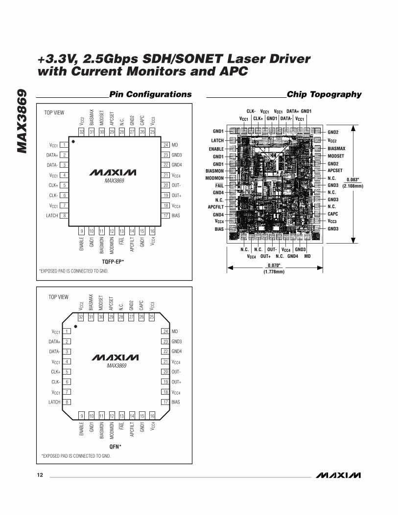
Pin Configurations Chip Topography
MAX3869
TOP VIEW
32 28293031 252627
BIAS
MAX
MOD
SET
APCS
ET
N.C.
V CC2
GND2
CAPC
V CC3
10 13 1514 1611 129
ENAB
LE
BIAS
MON
GND1 FAIL
MOD
MON
GND1
APCF
ILT
V CC4
17
18
19
20
21
22
23 GND3
24 MD
GND4
VCC4
OUT-
OUT+
VCC4
BIAS
2
3
4
5
6
7
8LATCH
VCC1
CLK-
CLK+
VCC1
DATA-
DATA+
1VCC1
TQFP-EP*
*EXPOSED PAD IS CONNECTED TO GND.
LATCH
GND1
VCC1 CLK+ GND1 DATA- VCC1
CLK- VCC1 VCC1 DATA+ GND1
ENABLE
GND1
GND1BIASMON
MODMON
FAILGND4
N.C.APCFILT
GND4VCC4
MDGND4N.C.OUT+VCC4
OUT-N.C. N.C. GND3VCC4
BIAS
VCC2
GND2
BIASMAX
MODSET
GND2APCSET
N.C.GND3N.C.
GND3N.C.
CAPCVCC3
GND3
0.083"(2.108mm)
0.070"(1.778mm)
MAX3869
TOP VIEW
32 28293031 252627
BIAS
MAX
MOD
SET
APCS
ET
N.C.
V CC2
GND2
CAPC
V CC3
10 13 1514 1611 129
ENAB
LE
BIAS
MON
GND1 FAIL
MOD
MON
GND1
APCF
ILT
V CC4
17
18
19
20
21
22
23 GND3
24 MD
GND4
VCC4
OUT-
OUT+
VCC4
BIAS
2
3
4
5
6
7
8LATCH
VCC1
CLK-
CLK+
VCC1
DATA-
DATA+
1VCC1
QFN*
*EXPOSED PAD IS CONNECTED TO GND.
MA
X3
86
9
+3.3V, 2.5Gbps SDH/SONET Laser Driver with Current Monitors and APC
______________________________________________________________________________________ 13
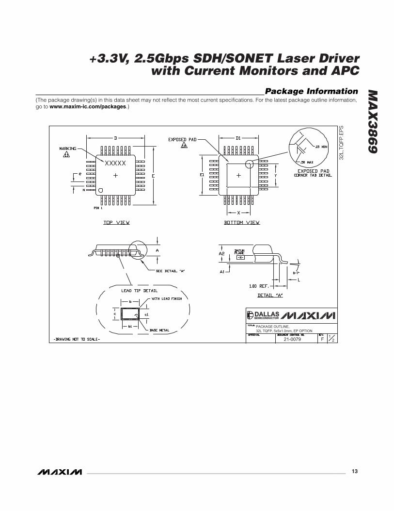
32L,
TQFP
.EP
SF 1
221-0079
PACKAGE OUTLINE,32L TQFP, 5x5x1.0mm, EP OPTION
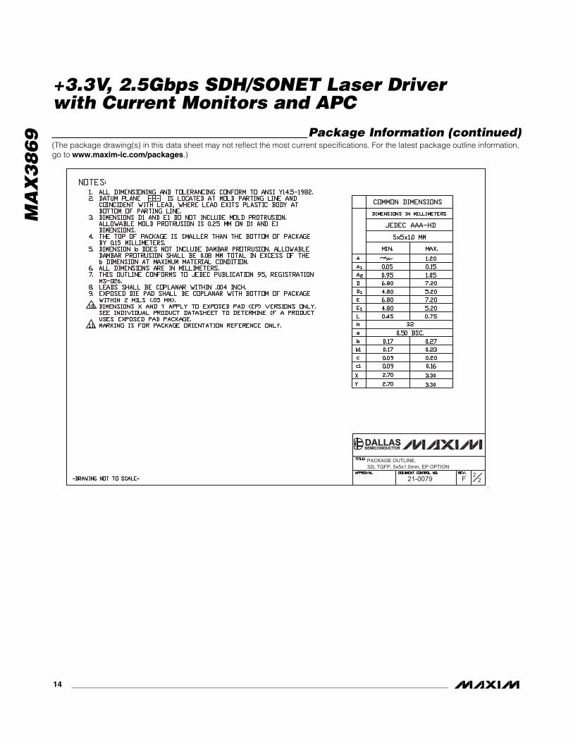
Package Information(The package drawing(s) in this data sheet may not reflect the most current specifications. For the latest package outline information,go to www.maxim-ic.com/packages.)
F 2221-0079
PACKAGE OUTLINE,32L TQFP, 5x5x1.0mm, EP OPTION
Package Information (continued)(The package drawing(s) in this data sheet may not reflect the most current specifications. For the latest package outline information,go to www.maxim-ic.com/packages.)
MA
X3
86
9
+3.3V, 2.5Gbps SDH/SONET Laser Driver with Current Monitors and APC
14 ______________________________________________________________________________________
Maxim cannot assume responsibility for use of any circuitry other than circuitry entirely embodied in a Maxim product. No circuit patent licenses areimplied. Maxim reserves the right to change the circuitry and specifications without notice at any time.
Maxim Integrated Products, 120 San Gabriel Drive, Sunnyvale, CA 94086 408-737-7600 ____________________ 15
© 2005 Maxim Integrated Products Printed USA is a registered trademark of Maxim Integrated Products, Inc.
MA
X3
86
9
+3.3V, 2.5Gbps SDH/SONET Laser Driver with Current Monitors and APC
32L
QFN
.EP
S
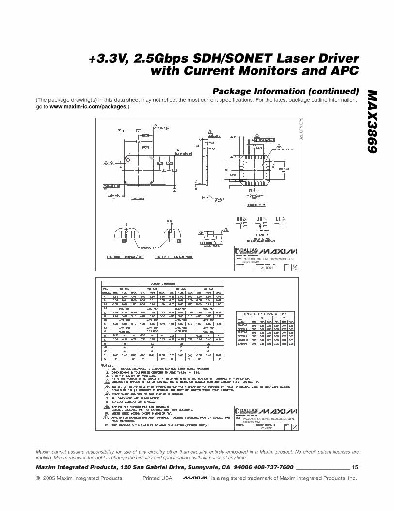
Package Information (continued)(The package drawing(s) in this data sheet may not reflect the most current specifications. For the latest package outline information,go to www.maxim-ic.com/packages.)


![三菱光デバイス - 三菱電機 Mitsubishi Electric...光通信用デバイス[2.5Gbps以下] セレクションマップ ~622Mbps 1.25Gbps 2.5Gbps Bit Rate FP-LD 1.3˜m 1.49˜m](https://static.fdocuments.in/doc/165x107/5f19d72bbe57380d65004985/eff-ee-mitsubishi-ecff25gbps.jpg)