EVALUATION KIT AVAILABLE 1.8V, Low-Power, 12-Bit, … integrated products... · General Description...
21
General Description The MAX1215N is a monolithic, 12-bit, 250Msps ana- log-to-digital converter (ADC) optimized for outstanding dynamic performance at high-IF frequencies beyond 300MHz. The product operates with conversion rates up to 250Msps while consuming only 886mW. At 250Msps and an input frequency of 100MHz, the MAX1215N achieves an 84.7dBc spurious-free dynam- ic range (SFDR) with e6.7dB signal-to-noise ratio (SNR) that remains flat (within 2dB) for input tones up to 250MHz. This makes it ideal for wideband applications such as communications receivers, cable-head end receivers, and power-amplifier predistortion in cellular base-station transceivers (BTS). The MAX1215N operates from a single 1.8V power sup- ply. The analog input is designed for AC-coupled differ- ential or single-ended operation. The ADC also features a selectable on-chip divide-by-2 clock circuit that accepts clock frequencies as high as 500MHz. A low-voltage dif- ferential signal (LVDS) sampling clock is recommended for best performance. The converter provides LVDS-com- patible digital outputs with data format selectable to be either two’s complement or offset binary. The MAX1215N is available in a 68-pin QFN package with exposed paddle (EP) and is specified over the indus- trial (-40°C to +85°C) temperature range. See the Pin-Compatible Versions table for a complete selection of 8-bit, 10-bit, and 12-bit high-speed ADCs in this family. Applications Base-Station Power-Amplifier Linearization Cable-Head End Receivers Wireless and Wired Broadband Communications Communications Test Equipment Radar and Satellite Subsystems Features ♦ 250Msps Conversion Rate ♦ Excellent Low-Noise Characteristics SNR = 66.7dB at f IN = 100MHz SNR = 65.6dB at f IN = 250MHz ♦ Excellent Dynamic Range SFDR = 84.7dBc at f IN = 100MHz SFDR = 80dBc at f IN = 250MHz ♦ Single 1.8V Supply ♦ 886mW Power Dissipation at f SAMPLE = 250Msps and f IN = 100MHz ♦ On-Chip Track-and-Hold Amplifier ♦ Internal 1.25V-Bandgap Reference ♦ On-Chip Selectable Divide-by-2 Clock Input ♦ LVDS Digital Outputs with Data Clock Output ♦ MAX1215NEVKIT Available MAX1215N 1.8V, Low-Power, 12-Bit, 250Msps ADC for Broadband Applications ________________________________________________________________ Maxim Integrated Products 1 19-0537; Rev 0; 4/06 For pricing, delivery, and ordering information, please contact Maxim/Dallas Direct! at 1-888-629-4642, or visit Maxim’s website at www.maxim-ic.com. EVALUATION KIT AVAILABLE Pin-Compatible Versions PART RESOLUTION (BITS) SPEED GRADE (Msps) ON-CHIP BUFFER MAX1121 8 250 Yes MAX1122 10 170 Yes MAX1123 10 210 Yes MAX1124 10 250 Yes MAX1213 12 170 Yes MAX1214 12 210 Yes MAX1215 12 250 Yes MAX1213N 12 170 No MAX1214N 12 210 No MAX1215N 12 250 No Pin Configuration appears at end of data sheet. PART TEMP RANGE PIN- PACKAGE PKG CODE MAX1215NEGK-D -40°C to +85°C 68 QFN-EP* G6800-4 MAX1215NEGK+D -40°C to +85°C 68 QFN-EP* G6800-4 Ordering Information *EP = Exposed paddle. +Denotes lead-free package. D = Dry pack.
Transcript of EVALUATION KIT AVAILABLE 1.8V, Low-Power, 12-Bit, … integrated products... · General Description...

General DescriptionThe MAX1215N is a monolithic, 12-bit, 250Msps ana-log-to-digital converter (ADC) optimized for outstandingdynamic performance at high-IF frequencies beyond300MHz. The product operates with conversion ratesup to 250Msps while consuming only 886mW.
At 250Msps and an input frequency of 100MHz, theMAX1215N achieves an 84.7dBc spurious-free dynam-ic range (SFDR) with e6.7dB signal-to-noise ratio (SNR)that remains flat (within 2dB) for input tones up to250MHz. This makes it ideal for wideband applicationssuch as communications receivers, cable-head endreceivers, and power-amplifier predistortion in cellularbase-station transceivers (BTS).
The MAX1215N operates from a single 1.8V power sup-ply. The analog input is designed for AC-coupled differ-ential or single-ended operation. The ADC also features aselectable on-chip divide-by-2 clock circuit that acceptsclock frequencies as high as 500MHz. A low-voltage dif-ferential signal (LVDS) sampling clock is recommendedfor best performance. The converter provides LVDS-com-patible digital outputs with data format selectable to beeither two’s complement or offset binary.
The MAX1215N is available in a 68-pin QFN packagewith exposed paddle (EP) and is specified over the indus-trial (-40°C to +85°C) temperature range.
See the Pin-Compatible Versions table for a completeselection of 8-bit, 10-bit, and 12-bit high-speed ADCs in this family.
ApplicationsBase-Station Power-Amplifier Linearization
Cable-Head End Receivers
Wireless and Wired Broadband Communications
Communications Test Equipment
Radar and Satellite Subsystems
Features 250Msps Conversion Rate Excellent Low-Noise Characteristics
SNR = 66.7dB at fIN = 100MHzSNR = 65.6dB at fIN = 250MHz
Excellent Dynamic RangeSFDR = 84.7dBc at fIN = 100MHzSFDR = 80dBc at fIN = 250MHz
Single 1.8V Supply
886mW Power Dissipation at fSAMPLE = 250Mspsand fIN = 100MHz
On-Chip Track-and-Hold Amplifier Internal 1.25V-Bandgap Reference On-Chip Selectable Divide-by-2 Clock Input LVDS Digital Outputs with Data Clock Output MAX1215NEVKIT Available
MA
X1
21
5N
1.8V, Low-Power, 12-Bit, 250Msps ADC for Broadband Applications
________________________________________________________________ Maxim Integrated Products 1
19-0537; Rev 0; 4/06
For pricing, delivery, and ordering information, please contact Maxim/Dallas Direct! at 1-888-629-4642, or visit Maxim’s website at www.maxim-ic.com.
EVALUATION KIT
AVAILABLE
Pin-Compatible Versions
PARTRESOLUTION
(BITS)
SPEEDGRADE(Msps)
ON-CHIPBUFFER
MAX1121 8 250 Yes
MAX1122 10 170 Yes
MAX1123 10 210 Yes
MAX1124 10 250 Yes
MAX1213 12 170 Yes
MAX1214 12 210 Yes
MAX1215 12 250 Yes
MAX1213N 12 170 No
MAX1214N 12 210 No
MAX1215N 12 250 NoPin Configuration appears at end of data sheet.
PART TEMP RANGEPIN-PACKAGE
PKGCODE
MAX1215NEGK-D -40°C to +85°C 68 QFN-EP* G6800-4
MAX1215NEGK+D -40°C to +85°C 68 QFN-EP* G6800-4
Ordering Information
*EP = Exposed paddle.+Denotes lead-free package.D = Dry pack.

MA
X1
21
5N
1.8V, Low-Power, 12-Bit, 250Msps ADC for Broadband Applications
2 ________________________________________________________________________________________
ABSOLUTE MAXIMUM RATINGS
ELECTRICAL CHARACTERISTICS(AVCC = OVCC = 1.8V, AGND = OGND = 0, fSAMPLE = 250MHz, differential clock input drive, 0.1µF capacitor on REFIO, internal ref-erence, digital output pins differential RL = 100Ω. Limits are for TA = -40°C to +85°C, unless otherwise noted. Typical values are at TA = +25°C.) (Note 1)
Stresses beyond those listed under “Absolute Maximum Ratings” may cause permanent damage to the device. These are stress ratings only, and functionaloperation of the device at these or any other conditions beyond those indicated in the operational sections of the specifications is not implied. Exposure toabsolute maximum rating conditions for extended periods may affect device reliability.
AVCC to AGND ......................................................-0.3V to +2.1VOVCC to OGND .....................................................-0.3V to +2.1VAVCC to OVCC .......................................................-0.3V to +2.1VAGND to OGND ....................................................-0.3V to +0.3VAnalog Inputs to AGND ...........................-0.3V to (AVCC + 0.3V)All Digital Inputs to AGND........................-0.3V to (AVCC + 0.3V)REFIO, REFADJ to AGND ........................-0.3V to (AVCC + 0.3V)All Digital Outputs to OGND ....................-0.3V to (OVCC + 0.3V)
ESD on All Pins (Human Body Model).............................±2000VCurrent into Any Pin..........................................................±50mAContinuous Power Dissipation (TA = +70°C, multilayer board)
68-Pin QFN-EP (derate 41.7mW/°C above +70°C)....3333mWOperating Temperature Range ...........................-40°C to +85°CJunction Temperature .....................................................+150°CStorage Temperature Range ............................-60°C to +150°CLead Temperature (soldering,10s) ..................................+300°C
PARAMETER SYMBOL CONDITIONS MIN TYP MAX UNITS
DC ACCURACY
Resolution 12 Bits
Integral Nonlinearity (Note 2) INL fIN = 10MHz -3 ±0.8 +3 LSB
Differential Nonlinearity (Note 2) DNL No missing codes -1.0 ±0.4 +1.3 LSB
Transfer Curve Offset VOS (Note 2) -3.5 +3.5 mV
Offset Temperature Drift ±20 µV/°C
ANALOG INPUTS (INP, INN)
Full-Scale Input Voltage Range VFS 1250 1385 mVP-P
Full-Scale Range TemperatureDrift
±60 ppm/°C
Common-Mode Input Voltage VCM Internally self-biased 0.7 V
Differential Input Capacitance CIN 2.5 pF
Differential Input Resistance RIN 1.8 kΩFull-Power Analog Bandwidth FPBW 700 MHz
REFERENCE (REFIO, REFADJ)
Reference Output Voltage VREFIO REFADJ = AGND 1.18 1.25 1.30 V
Reference Temperature Drift 90 ppm/°C
REFADJ Input High Voltage VREFADJ Used to disable the internal reference AVCC - 0.3 V
SAMPLING CHARACTERISTICS
Maximum Sampling Rate fSAMPLE 250 MHz
Minimum Sampling Rate fSAMPLE 20 MHz
Clock Duty Cycle Set by clock-management circuit 40 to 60 %
Aperture Delay tAD Figures 5, 11 620 ps
Aperture Jitter tAJ Figure 11 0.15 psRMS

MA
X1
21
5N
1.8V, Low-Power, 12-Bit, 250Msps ADC for Broadband Applications
_______________________________________________________________________________________ 3
ELECTRICAL CHARACTERISTICS (continued)(AVCC = OVCC = 1.8V, AGND = OGND = 0, fSAMPLE = 250MHz, differential clock input drive, 0.1µF capacitor on REFIO, internal ref-erence, digital output pins differential RL = 100Ω. Limits are for TA = -40°C to +85°C, unless otherwise noted. Typical values are at TA = +25°C.) (Note 1)
PARAMETER SYMBOL CONDITIONS MIN TYP MAX UNITS
CLOCK INPUTS (CLKP, CLKN)
Differential Clock Input Amplitude (Note 3) 200 500 mVP-P
Clock Input Common-ModeVoltage Range
Internally self-biased 1.15 ±0.25 V
Clock Differential InputResistance
RCLK 11 ±25% kΩ
Clock Differential InputCapacitance
CCLK 5 pF
DYNAMIC CHARACTERISTICS (at AIN = -1dBFS)
fIN = 10MHz 64.5 67
fIN = 100MHz 64.3 66.7
fIN = 200MHz 66.1Signal-to-Noise Ratio SNR
fIN = 250MHz 65.6
dB
fIN = 10MHz 63.5 66.8
fIN = 100MHz 63.3 66.4
fIN = 200MHz 65.9Signal-to-Noiseand Distortion
SINAD
fIN = 250MHz 65.4
dB
fIN = 10MHz 70 86
fIN = 100MHz 70 84.7
fIN = 200MHz 83.4Spurious-FreeDynamic Range
SFDR
fIN = 250MHz 80
dBc
fIN = 10MHz -86 -70
fIN = 100MHz -84.7 -70
fIN = 200MHz -83.4Worst Harmonics(HD2 or HD3)
fIN = 250MHz -80
dBc
Two-Tone IntermodulationDistortion
TTIMDfIN1 = 99MHz at AIN1 = -7dBFS,fIN2 = 101MHz at AIN2 = -7dBFS
-86.9 dBc
LVDS DIGITAL OUTPUTS (D0P/N–D11P/N, ORP/N)
Differential Output Voltage |VOD| RL = 100Ω 280 440 mV
Output Offset Voltage OVOS RL = 100Ω 1.11 1.37 V

MA
X1
21
5N
1.8V, Low-Power, 12-Bit, 250MspsADC for Broadband Applications
4 ________________________________________________________________________________________
ELECTRICAL CHARACTERISTICS (continued)(AVCC = OVCC = 1.8V, AGND = OGND = 0, fSAMPLE = 250MHz, differential clock input drive, 0.1µF capacitor on REFIO, internal ref-erence, digital output pins differential RL = 100Ω. Limits are for TA = -40°C to +85°C, unless otherwise noted. Typical values are at TA = +25°C.) (Note 1)
PARAMETER SYMBOL CONDITIONS MIN TYP MAX UNITS
LVCMOS DIGITAL INPUTS (CLKDIV, T/B)
Digital Input-Voltage Low VIL 0.2 x AVCC V
Digital Input-Voltage High VIH 0.8 x AVCC V
TIMING CHARACTERISTICS
CLK-to-Data Propagation Delay tPDL Figure 5 2.23 ns
CLK-to-DCLK Propagation Delay tCPDL Figure 5 3.77 ns
DCLK-to-Data Propagation Delay tCPDL - tPDL Figure 5 (Note 3) 1.47 1.54 1.63 ns
LVDS Output Rise Time tRISE 20% to 80%, CL = 5pF 155 ps
LVDS Output Fall Time tFALL 20% to 80%, CL = 5pF 145 ps
Output Data Pipeline Delay tLATENCY Figure 5 11Clockcycles
POWER REQUIREMENTS
Analog Supply Voltage Range AVCC 1.7 1.8 1.9 V
Digital Supply Voltage Range OVCC 1.7 1.8 1.9 V
Analog Supply Current IAVCC fIN = 100MHz 428 480 mA
Digital Supply Current IOVCC fIN = 100MHz 64 74 mA
Analog Power Dissipation PDISS fIN = 100MHz 886 965 mW
Offset 1.7 mV/VPower-Supply Rejection Ratio(Note 4)
PSRRGain 4.5 %FS/V
Note 1: TA ≥ +25°C guaranteed by production test, TA < +25°C guaranteed by design and characterization. Typical values are atTA = +25°C
Note 2: Static linearity and offset parameters are computed from an endpoint curve fit.Note 3: Parameter guaranteed by design and characterization: TA = -40°C to +85°C.Note 4: PSRR is measured with both analog and digital supplies connected to the same potential.

MA
X1
21
5N
1.8V, Low-Power, 12-Bit, 250Msps ADC for Broadband Applications
_______________________________________________________________________________________ 5
FFT PLOT (8192-POINT DATA RECORD)
MAX
1215
N to
c010
3
25
4
0 4020 60 80 100 120ANALOG INPUT FREQUENCY (MHz)
-100-110
-90-80-70-60-50-40-30-20-10
-120
fSAMPLE = 250MHz fIN = 11.566MHz AIN = -0.982dBFS SNR = 67.1dB SINAD = 66.953dB THD = -82.5dBc SFDR = 84.7dBc HD2 = -94.9dBcHD3 = -84.7dBc
AMPL
ITUD
E (d
BFS)
FFT PLOT (8192-POINT DATA RECORD)
MAX
1215
N to
c02
AMPL
ITUD
E (d
BFS)
-100-110
-90-80-70-60-50-40-30-20-10
0
-120
2
0 4020 60 80 100 120ANALOG INPUT FREQUENCY (MHz)
43 5
fSAMPLE = 250MHz fIN = 65.033MHz AIN = -1.008dBFS SNR = 67dB SINAD = 66.9dB THD = -83.6dBc SFDR = 87dBc HD2 = -87dBcHD3 = -81.8dBc
FFT PLOT (8192-POINT DATA RECORD)
MAX
1215
N to
c03
AMPL
ITUD
E (d
BS)
-100-110
-90-80-70-60-50-40-30-20-10
0
-1200 4020 60 80 100 120
ANALOG INPUT FREQUENCY (MHz)
5 34 2
fSAMPLE = 250MHz fIN = 199.249MHz AIN = -1.004dBFS SNR = 66dB SINAD = 65.9dB THD = -81dBc SFDR = 82.7dBcHD2 = -90.9dBcHD3 = -82.7dBc
FFT PLOT (8192-POINT DATA RECORD)
MAX
1215
N to
c04
AMPL
ITUD
E (d
BS)
-100-110
-90-80-70-60-50-40-30-20-10
0
-1200 4020 60 80 100 120
ANALOG INPUT FREQUENCY (MHz)
4
fSAMPLE = 250MHzfIN = 248.627MHzAIN = -0.933dBFSSNR = 65.4dBSINAD = 65.185dBTHD = -78dBcSFDR = 82.7dBcHD2 = -82.7dBcHD3 = -83.1dBc2
3 5
TWO-TONE IMD PLOT(32,768-POINT DATA RECORD)
MAX
1215
N to
c05
ANALOG INPUT FREQUENCY (MHz)
AMPL
ITUD
E (d
BFS)
100755025
-100
-75
-50
-25
0
-1250 125
fSAMPLE = 250MHzfIN1 = 99MHzfIN2 = 101MHzIMD = -86dBc
SNR/SINAD vs. ANALOG INPUT FREQUENCY(fSAMPLE = 250MHz, AIN = -1dBFS)
fIN (MHz)
SNR/
SINA
D (d
B)
MAX
1215
N to
c06
0 50 100 150 200 250 30052
55
58
61
64
67
70SNR
SINAD
SFDR vs. ANALOG INPUT FREQUENCY(fSAMPLE = 250MHz, AIN = -1dBFS)
fIN (MHz)
SFDR
(dBc
)
MAX
1215
N to
c07
0 50 100 150 200 250 30065
70
75
80
85
90
HD2/HD3 vs. ANALOG INPUT FREQUENCY(fSAMPLE = 250MHz, AIN = -1dBFS)
fIN (MHz)
HD2/
HD3
(dBc
)
MAX
1215
N to
c08
0 50 100 150 200 250 300-100-96-92-88-84-80-76-72-68-64-60-56-52
HD2
HD3
SNR/SINAD vs. ANALOG INPUT AMPLITUDE(fSAMPLE = 250MHz, fIN = 65.033MHz)
ANALOG INPUT AMPLITUDE (dBFS)
SNR/
SINA
D (d
B)
MAX
1215
N to
c09
-55 -50 -45 -40 -35 -30 -25 -20 -15 -10 -5 010152025303540455055606570
SNRSINAD
Typical Operating Characteristics(AVCC = OVCC = 1.8V, AGND = OGND = 0, fSAMPLE = 250MHz, AIN = -1dBFS, see each TOC for detailed information on test condi-tions, differential input drive, differential sine-wave clock input drive, 0.1µF capacitor on REFIO, internal reference, digital output pinsdifferential RL = 100Ω, TA = +25°C.)

MA
X1
21
5N
1.8V, Low-Power, 12-Bit, 250MspsADC for Broadband Applications
6 ________________________________________________________________________________________
SFDR vs. ANALOG INPUT AMPLITUDE(fSAMPLE = 250MHz, fIN = 65.033MHz)
ANALOG INPUT AMPLITUDE (dBFS)
SFDR
(dBc
)
MAX
1215
N to
c10
-55 -50 -45 -40 -35 -30 -25 -20 -15 -10 -5 035
40
45
50
55
60
65
70
75
80
HD2/HD3 vs. ANALOG INPUT AMPLITUDE(fSAMPLE = 250MHz, fIN = 65.033MHz)
ANALOG INPUT AMPLITUDE (dBFS)
HD2/
HD3
(dBc
)
MAX
1215
N to
c11
-55 -50 -45 -40 -35 -30 -25 -20 -15 -10 -5 0-100-95-90-85-80-75-70-65-60-55-50-45-40-35-30
HD2
HD3
SNR/SINAD vs. SAMPLE FREQUENCY(fIN = 65MHz, AIN = -1dBFS)
fSAMPLE (MHz)
SNR/
SINA
D (d
B)
MAX
1215
N to
c12
0 50 100 150 200 25060
62
64
66
68
70
SNR
SINAD
SFDR vs. SAMPLE FREQUENCY(fIN = 65MHz, AIN = -1dBFS)
fSAMPLE (MHz)
SFDR
(dBc
)
MAX
1215
N to
c13
0 25 50 75 100 125 150 175 200 225 25070
72
74
76
78
80
82
84
86
88
90
HD2/HD3 vs. SAMPLE FREQUENCY(fIN = 65MHz, AIN = -1dBFS)
fSAMPLE (MHz)
HD2/
HD3
(dBc
)
MAX
1215
N to
c14
0 50 100 150 200 250-100
-96
-92
-88
-84
-80
-76
-72
HD2
HD3
TOTAL POWER DISSIPATION vs. SAMPLE FREQUENCY(fIN = 65.033MHz, AIN = -1dBFS)
fSAMPLE (MHz)
P DIS
S (W
)
MAX
1215
N to
c15
0 50 100 150 200 2500.750
0.775
0.800
0.825
0.850
0.875
0.900
INTEGRAL NONLINEARITYvs. DIGITAL OUTPUT CODE
MAX
1215
N to
c16
DIGITAL OUTPUT CODE
INL
(LSB
)
1365 2730
-0.3
0.2
0.7
-0.80 4095
DIFFERENTIAL NONLINEARITYvs. DIGITAL OUTPUT CODE
MAX
1215
N to
c17
DIGITAL OUTPUT CODE
DNL
(LSB
)
1365 2729
-0.2
0
0.2
-0.50 4094
GAIN BANDWIDTH PLOT(fSAMPLE = 250MHz, NORMALIZED TO 0dB)
ANALOG INPUT FREQUENCY (MHz)
GAIN
(dB)
MAX
1215
toc1
8
-5.0
-4.5
-4.0
-3.5
-3.0
-2.5
-2.0
-1.5
-1.0
-0.5
0
10 100 1000
Typical Operating Characteristics (continued)(AVCC = OVCC = 1.8V, AGND = OGND = 0, fSAMPLE = 250MHz, AIN = -1dBFS, see each TOC for detailed information on test condi-tions, differential input drive, differential sine-wave clock input drive, 0.1µF capacitor on REFIO, internal reference, digital output pinsdifferential RL = 100Ω, TA = +25°C.)
Typical Operating Characteristics (continued)(AVCC = OVCC = 1.8V, AGND = OGND = 0, fSAMPLE = 250MHz, AIN = -1dBFS, see each TOC for detailed information on test condi-tions, differential input drive, differential sine-wave clock input drive, 0.1µF capacitor on REFIO, internal reference, digital output pinsdifferential RL = 100Ω, TA = +25°C.)

MA
X1
21
5N
SNR/SINAD vs. TEMPERATURE(fIN = 65MHz, AIN = -1dBFS)
TEMPERATURE (°C)
SNR/
SINA
D (d
B)
MAX
1215
N to
c19
-40 -15 10 35 60 8560
62
64
66
68
70
SNR
SINAD
SFDR vs. TEMPERATURE(fIN = 65MHz, AIN = -1dBFS)
TEMPERATURE (°C)
SFDR
(dBc
)
MAX
1215
N to
c20
-40 -15 10 35 60 8570
72
74
76
78
80
82
84
86
88
90
HD2/HD3 vs. TEMPERATURE(fIN = 65MHz, AIN = -1dBFS)
TEMPERATURE (°C)
HD2/
HD3
(dBc
)
MAX
1215
N to
c21
-40 -15 10 35 60 85-100
-96
-92
-88
-84
-80
-76
-72
HD2
HD3
1.8V, Low-Power, 12-Bit, 250Msps ADC for Broadband Applications
_______________________________________________________________________________________ 7
SNR/SINAD vs. SUPPLY VOLTAGE(fIN = 65.033MHz, AIN = -1dBFS)
SUPPLY VOLTAGE (V)
SNR/
SINA
D (d
B)
MAX
1215
N to
c22
1.70 1.75 1.80 1.85 1.9060
62
64
66
68
70
SNR
SINAD
SFDR vs. SUPPLY VOLTAGE(fIN = 65.033MHz, AIN = -1dBFS)
SUPPLY VOLTAGE (V)
SFDR
(dBc
)
MAX
1215
N to
23
1.70 1.75 1.80 1.85 1.9072
74
76
78
80
82
84
86
88
90
HD2/HD3 vs. SUPPLY VOLTAGE(fIN = 65.033MHz, AIN = -1dBFS)
SUPPLY VOLTAGE (V)
HD2/
HD3
(dBc
)
MAX
1215
N to
c24
1.70 1.75 1.80 1.85 1.90-100
-95
-90
-85
-80
-75
HD2
HD3
REFERENCE vs. SUPPLY VOLTAGE(fIN = 65.033MHz, AIN = -1dBFS)
SUPPLY VOLTAGE (V)
V REF
IO (V
)
MAX
1215
N to
c25
1.70 1.75 1.80 1.85 1.901.246
1.247
1.248
1.249
1.250
1.251
1.252
1.253
1.254
Typical Operating Characteristics (continued)(AVCC = OVCC = 1.8V, AGND = OGND = 0, fSAMPLE = 250MHz, AIN = -1dBFS, see each TOC for detailed information on test condi-tions, differential input drive, differential sine-wave clock input drive, 0.1µF capacitor on REFIO, internal reference, digital output pinsdifferential RL = 100Ω, TA = +25°C.)
Typical Operating Characteristics (continued)(AVCC = OVCC = 1.8V, AGND = OGND = 0, fSAMPLE = 250MHz, AIN = -1dBFS, see each TOC for detailed information on test condi-tions, differential input drive, differential sine-wave clock input drive, 0.1µF capacitor on REFIO, internal reference, digital output pinsdifferential RL = 100Ω, TA = +25°C.)

MA
X1
21
5N
1.8V, Low-Power, 12-Bit, 250Msps ADC for Broadband Applications
8 ________________________________________________________________________________________
Pin Description
PIN NAME FUNCTION
1, 6, 11–14, 20,25, 62, 63, 65
AVCC
Analog Supply Voltage. Bypass AVCC to AGND with a parallel combination of 0.1µF and 0.22µFcapacitors for best decoupling results. Connect all AVCC inputs together. See the Grounding,Bypassing, and Layout Considerations section.
2, 5, 7, 10, 15, 16,18, 19, 21, 24,
64, 66, 67AGND Analog Converter Ground. Connect all AGND inputs together.
3 REFIOReference Input/Output. Pull REFADJ high to allow REFIO to accept an external reference. PullREFADJ low to activate the internal 1.25V-bandgap reference. Connect a 0.1µF capacitor fromREFIO to AGND for both internal and external reference.
4 REFADJ
Reference Adjust Input. REFADJ allows for FSR adjustments by placing a resistor or trimpotentiometer between REFADJ and AGND (decreases FSR) or REFADJ and REFIO (increasesFSR). Connect REFADJ to AVCC to override the internal reference with an external sourceconnected to REFIO. Connect REFADJ to AGND to allow the internal reference to determine theFSR of the data converter. See the FSR Adjustment Using the Internal Reference section.
8 INP Positive Analog Input Terminal. Internally self-biased to 0.7V.
9 INN Negative Analog Input Terminal. Internally self-biased to 0.7V.
17 CLKDIV
Clock Divider Input. CLKDIV controls the sampling frequency relative to the input clockfrequency. CLKDIV has an internal pulldown resistor.CLKDIV = 0: Sampling frequency is at one-half the input clock frequency.CLKDIV = 1: Sampling frequency is equal to the input clock frequency.
22 CLKP Tr ue C l ock Inp ut. Ap p l y an LV D S - com p ati b l e i np ut l evel to C LKP . Inter nal l y sel f- b i ased to 1.15V .
23 CLKNComplementary Clock Input. Apply an LVDS-compatible input level to CLKN. Internally self-biased to 1.15V .
26, 45, 61 OGNDDigital Converter Ground. Ground connection for digital circuitry and output drivers. Connect allOGND inputs together.
27, 28, 41, 44, 60 OVCCDigital Supply Voltage. Bypass OVCC with a 0.1µF capacitor to OGND. Connect all OVCC inputstogether. See the Grounding, Bypassing, and Layout Considerations section.
29 D0N Complementary Output Bit 0 (LSB)
30 D0P True Output Bit 0 (LSB)
31 D1N Complementary Output Bit 1
32 D1P True Output Bit 1
33 D2N Complementary Output Bit 2
34 D2P True Output Bit 2
35 D3N Complementary Output Bit 3
36 D3P True Output Bit 3

MA
X1
21
5N
1.8V, Low-Power, 12-Bit, 250Msps ADC for Broadband Applications
_______________________________________________________________________________________ 9
Pin Description (continued)
PIN NAME FUNCTION
37 D4N Complementary Output Bit 4
38 D4P True Output Bit 4
39 D5N Complementary Output Bit 5
40 D5P True Output Bit 5
42 DCLKNComplementary Clock Output. This output provides an LVDS-compatible output level and canbe used to synchronize external devices to the converter clock.
43 DCLKPTrue Clock Output. This output provides an LVDS-compatible output level and can be used tosynchronize external devices to the converter clock.
46 D6N Complementary Output Bit 6
47 D6P True Output Bit 6
48 D7N Complementary Output Bit 7
49 D7P True Output Bit 7
50 D8N Complementary Output Bit 8
51 D8P True Output Bit 8
52 D9N Complementary Output Bit 9
53 D9P True Output Bit 9
54 D10N Complementary Output Bit 10
55 D10P True Output Bit 10
56 D11N Complementary Output Bit 11 (MSB)
57 D11P True Output Bit 11 (MSB)
58 ORNComplementary Out-of-Range Control Bit Output. If an out-of-range condition is detected,bit ORN flags this condition by transitioning low.
59 ORPTrue Out-of-Range Control Bit Output. If an out-of-range condition is detected, bit ORP flagsthis condition by transitioning high.
68 T/B
Output Format Select Input. This LVCMOS-compatible input controls the digital output format ofthe MAX1215N. T/B has an internal pulldown resistor.T/B = 0: Two’s-complement output format.T/B = 1: Binary output format.
— EPExposed Paddle. The exposed paddle is located on the backside of the chip and must beconnected to AGND.

MA
X1
21
5N
1.8V, Low-Power, 12-Bit, 250Msps ADC for Broadband Applications
10 ______________________________________________________________________________________
Detailed Description—Theory of Operation
The MAX1215N uses a fully differential pipelined archi-tecture that allows for high-speed conversion, opti-mized accuracy, and linearity while minimizing powerconsumption.
Both positive (INP) and negative analog input terminals(INN) are centered around a 0.7V common-mode volt-age, and accept a differential analog input voltageswing of ±VFS / 4 each, resulting in a typical 1.385VP-Pdifferential full-scale signal swing. Inputs INP and INNare sampled when the differential sampling clock sig-nal transitions high. When using the clock-dividemode, the analog inputs are sampled at every otherhigh transition of the differential sampling clock.
Each pipeline converter stage converts its input voltageto a digital output code. At every stage, except the last,the error between the input voltage and the digital out-put code is multiplied and passed along to the nextpipeline stage. Digital error correction compensates for
ADC comparator offsets in each pipeline stage andensures no missing codes. The result is a 12-bit paralleldigital output word in user-selectable two’s-complementor offset binary output formats with LVDS-compatibleoutput levels. See Figure 1 for a more detailed view ofthe MAX1215N architecture.
Analog Inputs (INP, INN)INP and INN are the fully differential inputs of theMAX1215N. Differential inputs usually feature goodrejection of even-order harmonics, which allows forenhanced AC performance as the signals are progress-ing through the analog stages. The MAX1215N analoginputs are self-biased at a 0.7V common-mode voltageand allow a 1.385VP-P differential input voltage swing(Figure 2). Both inputs are self-biased through 900Ωresistors, resulting in a typical differential input resis-tance of 1.8kΩ. Drive the analog inputs of theMAX1215N in AC-coupled configuration to achievebest dynamic performance. See the Transformer-Coupled, Differential Analog Input Drive section.
MAX1215N
AVCC
900Ω900Ω
D0P/N
DCLKP
DCLKN
D1P/N
D2P/NLVDSDATA PORT
OVCC
AGND OGND
T/H 12-BIT PIPELINEADC
CLOCKMANAGEMENTREFERENCE
COMMON-MODE BUFFER
CLKDIV
CLKNCLKP
REFADJ
REFIO
INP
INN
DIV1/DIV2
D11P/N
ORP/ORN
T/B
Figure 1. Block Diagram

MA
X1
21
5N
1.8V, Low-Power, 12-Bit, 250Msps ADC for Broadband Applications
______________________________________________________________________________________ 11
MAX1215N
12-BIT PIPELINEADC
CS
FROM CLOCK-MANAGEMENT BLOCK
T/H
TO COMMON MODE
CS
CP
INP
INP
INP - INN
VCM + VFS / 4
VCM - VFS / 4
+VFS / 2
-VFS / 2
GND
GND
VCM
INN
INN
CS IS THE SAMPLING CAPACITANCECP IS THE PARASITIC CAPACITANCE ~ 1pF
AVCC
900Ω
900Ω
CP1.
385V
DIF
FERE
NTIA
L FS
R
Figure 2. Simplified Analog Input Architecture and Allowable Input Voltage Range

MA
X1
21
5N
1.8V, Low-Power, 12-Bit, 250Msps ADC for Broadband Applications
12 _______________________________________________________________________________________
On-Chip Reference CircuitThe MAX1215N features an internal 1.25V-bandgap refer-ence circuit (Figure 3), which, in combination with aninternal reference-scaling amplifier, determines the FSRof the MAX1215N. Bypass REFIO with a 0.1µF capacitorto AGND. To compensate for gain errors or increase/de-crease the ADC’s FSR, the voltage of this bandgap refer-ence can be indirectly adjusted by adding an externalresistor (e.g., 100kΩ trim potentiometer) betweenREFADJ and AGND or REFADJ and REFIO. See theApplications Information section for a detailed descriptionof this process.
To disable the internal reference, connect REFADJ toAVCC. Apply an external, stable reference at REFIO toset the converter’s full scale. To enable the internal ref-erence, connect REFADJ to AGND.
Clock Inputs (CLKP, CLKN)Drive the clock inputs of the MAX1215N with an LVDS- orLVPECL-compatible clock to achieve the best dynamicperformance. The clock signal source must be of highquality and low phase noise to avoid any degradation inthe noise performance of the ADC. The clock inputs(CLKP, CLKN) are internally biased to 1.15V, accept atypical 500mVP-P differential signal swing (Figure 4). Seethe Differential, AC-Coupled LVPECL-Compatible ClockInput section for more circuit details on how to driveCLKP and CLKN appropriately. Although not recom-mended, the clock inputs also accept a single-endedinput signal.
The MAX1215N also features an internal clock-manage-ment circuit (duty-cycle equalizer) that ensures theclock signal applied to inputs CLKP and CLKN isprocessed to provide a 50% duty-cycle clock signalthat desensitizes the performance of the converter tovariations in the duty cycle of the input clock source.Note that the clock duty-cycle equalizer cannot beturned off externally and requires a minimum 20MHzclock frequency to allow the device to meet data sheetspecifications.
Data Clock Outputs (DCLKP, DCLKN)The MAX1215N features a differential clock output,which can be used to latch the digital output data withan external latch or receiver. Additionally, the clock out-put can be used to synchronize external devices (e.g.,FPGAs) to the ADC. DCLKP and DCLKN are differentialoutputs with LVDS-compatible voltage levels. There is a3.77ns delay time between the rising (falling) edge ofCLKP (CLKN) and the rising (falling) edge of DCLKP(DCLKN). See Figure 5 for timing details.
Divide-by-2 Clock Control (CLKDIV)The MAX1215N offers a clock control line (CLKDIV),which supports the reduction of clock jitter in a system.Connect CLKDIV to OGND to enable the ADC’s internaldivide-by-2 clock divider. Data is now updated at one-half the ADC’s input clock rate. CLKDIV has an internalpulldown resistor and can be left open for applicationsthat require this divide-by-2 mode. Connecting CLKDIVto OVCC disables the divide-by-2 mode.
MAX1215N
REFERENCEBUFFER
ADC FULL SCALE = REFT - REFB
REFT: TOP OF REFERENCE LADDER.REFB: BOTTOM OF REFERENCE LADDER.
1V
AVCC AVCC / 2
G
CONTROL LINE TODISABLE REFERENCE BUFFER
REFERENCE- SCALING AMPLIFIER
REFIO
REFADJ*
0.1µF
100Ω*
*REFADJ MAYBE SHORTED TOAGND DIRECTLY
REFT
REFB
Figure 3. Simplified Reference Architecture

MA
X1
21
5N
1.8V, Low-Power, 12-Bit, 250Msps ADC for Broadband Applications
______________________________________________________________________________________ 13
System Timing RequirementsFigure 5 depicts the relationship between the clockinput and output, analog input, sampling event, anddata output. The MAX1215N samples on the rising(falling) edge of CLKP (CLKN). Output data is valid onthe next rising (falling) edge of the DCLKP (DCLKN)clock, but has an internal latency of 11 clock cycles.
Digital Outputs (D0P/N–D11P/N, DCLKP/N,ORP/N) and Control Input T/B
Digital outputs D0P/N–D11P/N, DCLKP/N, and ORP/Nare LVDS compatible, and data on D0P/N–D11P/N ispresented in either binary or two’s-complement format(Table 1). The T/B control line is an LVCMOS-compati-ble input, which allows the user to select the desiredoutput format. Pulling T/B low outputs data in two’scomplement, and pulling it high presents data in offsetbinary format on the 12-bit parallel bus. T/B has aninternal pulldown resistor and may be left unconnectedin applications using only two’s-complement output for-mat. All LVDS outputs provide a typical 360mV voltageswing around a 1.24V common-mode voltage, and mustbe terminated at the far end of each transmission line pair(true and complementary) with 100Ω. Apply a 1.7V to1.9V voltage supply at OVCC to power the LVDS outputs.
The MAX1215N offers an additional differential outputpair (ORP, ORN) to flag out-of-range conditions, whereout-of-range is above positive or below negative fullscale. An out-of-range condition is identified with ORP(ORN) transitioning high (low).
Note: Although a differential LVDS output architecturereduces single-ended transients to the supply andground planes, capacitive loading on the digital out-puts should still be kept as low as possible. UsingLVDS buffers on the digital outputs of the ADC whendriving larger loads may improve overall performanceand reduce system-timing constraints.
INP
INN
SAMPLING EVENT SAMPLING EVENT SAMPLING EVENT SAMPLING EVENT SAMPLING EVENT
CLKN
CLKP
DCLKN
DCLKP
D0P/D0N–D11P/D11N
ORP/N
N
N-11 N-10 N - 1 N + 1N
NN - 1N - 9N - 10N - 11 N + 1
N + 1 N + 11N + 10 N + 12
tAD
tPDL tLATENCY
tCPDL
tCPDL - tPDL~ 0.4 x tSAMPLE WITH tSAMPLE = 1 / fSAMPLENOTE: THE ADC SAMPLES ON THE RISING EDGE OF CLKP. THE RISING EDGE OF DCLKP CAN BE USED TO EXTERNALLY LATCH THE OUTPUT DATA.
tCH tCL
Figure 5. System and Output Timing Diagram
2.89kΩ
AVDD
AGND
CLKN
CLKP
5.35kΩ
5.35kΩ
5.35kΩ
Figure 4. Simplified Clock Input Architecture

MA
X1
21
5N
1.8V, Low-Power, 12-Bit, 250Msps ADC for Broadband Applications
14 _______________________________________________________________________________________
Applications InformationFSR Adjustments Using the Internal
Bandgap ReferenceThe MAX1215N supports a 10% (±5%) full-scaleadjustment range. To decrease the full-scale signalrange, add an external resistor value ranging from13kΩ to 1MΩ between REFADJ and AGND. Adding avariable resistor, potentiometer, or predetermined resis-
tor value between REFADJ and REFIO increases theFSR of the data converter. Figure 6a shows the twopossible configurations and their impact on the overallfull-scale range adjustment of the MAX1215N. Do notuse resistor values of less than 13kΩ to avoid instabilityof the internal gain regulation loop for the bandgap ref-erence. See Figure 6b for the resulting FSR for a seriesof resistor values.
Table 1. MAX1215N Digital Output CodingINP ANALOG
INPUT VOLTAGELEVEL
INN ANALOGINPUT VOLTAGE
LEVEL
OUT-OF-RANGEORP (ORN)
BINARY DIGITAL OUTPUTCODE (D11P/N–D0P/N)
TWO’S-COMPLEMENT DIGITALOUTPUT CODE (D11P/N–D0P/N)
> VCM + VFS / 4 < VCM - VFS / 4 1 (0)1111 1111 1111
(exceeds +FS, OR set)0111 1111 1111
(exceeds +FS, OR set)
VCM + VFS / 4 VCM - VFS / 4 0 (1) 1111 1111 1111 (+FS) 0111 1111 1111 (+FS)
VCM VCM 0 (1)1000 0000 0000 or
0111 1111 1111 (FS/2)0000 0000 0000 or
1111 1111 1111 (FS/2)
VCM - VFS / 4 VCM + VFS / 4 0 (1) 0000 0000 0000 (-FS) 1000 0000 0000 (-FS)
< VCM + VFS / 4 > VCM - VFS / 4 1 (0)0000 0000 0000
(exceeds -FS, OR set)1000 0000 0000
(exceeds -FS, OR set)
MAX1215N
REFERENCEBUFFER
ADC FULL SCALE = REFT - REFB
CONFIGURATION TO INCREASE THE FSR OF THE MAX1215N
REFT: TOP OF REFERENCE LADDER.REFB: BOTTOM OF REFERENCE LADDER.
1V
AVCC AVCC / 2
G
CONTROL LINE TO DISABLE
REFERENCE BUFFER
REFERENCE- SCALING AMPLIFIER
REFIO
REFADJ
0.1µF
REFT
REFB
13kΩ TO1MΩ
MAX1215N
REFERENCEBUFFER
ADC FULL SCALE = REFT - REFB
CONFIGURATION TO DECREASE THE FSR OF THE MAX1215N
1V
AVCC AVCC / 2
G
CONTROL LINE TO DISABLE
REFERENCE BUFFER
REFERENCE- SCALING AMPLIFIER
REFIO
REFADJ
0.1µF
REFT
REFB
13kΩ TO1MΩ
Figure 6a. Circuit Suggestions to Adjust the ADC’s Full-Scale Range

MA
X1
21
5N
1.8V, Low-Power, 12-Bit, 250Msps ADC for Broadband Applications
______________________________________________________________________________________ 15
Differential, AC-Coupled,LVPECL-Compatible Clock Input
The MAX1215N dynamic performance depends on theuse of a very clean clock source. The phase noise floorof the clock source has a negative impact on the SNRperformance. Spurious signals on the clock signalsource also affect the ADC’s dynamic range. The pre-ferred method of clocking the MAX1215N is differential-ly with LVDS- or LVPECL-compatible input levels. Thefast data transition rates of these logic families minimizethe clock-input circuitry’s transition uncertainty, therebyimproving the SNR performance. To accomplish this, a50Ω reverse-terminated clock signal source with lowphase noise is AC-coupled into a fast differentialreceiver such as the MC100LVEL16 (Figure 7). Thereceiver produces the necessary LVPECL output levelsto drive the clock inputs of the data converter.
Transformer-Coupled,Differential Analog Input Drive
The MAX1215N provides the best SFDR and THD withfully differential input signals and it is not recommend-ed to drive the ADC inputs in single-ended configura-tion. In differential input mode, even-order harmonicsare usually lower since INP and INN are balanced, and
FS VOLTAGE vs. ADJUST RESISTOR
FS ADJUST RESISTOR (kΩ)
V FS
(V)
1.16
1.18
1.20
1.22
1.24
1.26
1.28
1.30
1.32
1.34
1.14
RESISTOR VALUE APPLIED BETWEENREFADJ AND REFIO INCREASES VFS
RESISTOR VALUE APPLIED BETWEENREFADJ AND AGND DECREASES VFS
900800600 700200 300 400 5001000 1000
Figure 6b. FS Adjustment Range vs. FS Adjustment Resistor
MC100LVEL16D
AGND OGND
D0P/N–D11P/N, 0RP/N
AVCC
VCLK
0.1µF
0.1µF
0.1µF
0.1µF
0.01µF
SINGLE-ENDEDINPUT TERMINAL
150Ω
150Ω
CLKPCLKNINP
INN
OVCC
12
2
8
4 5
7
63
50Ω
10kΩ
510Ω510Ω
MAX1215N
Figure 7. Differential, AC-Coupled, LVPECL-Compatible Clock Input Configuration
MA
X1
21
5N
1.8V, Low-Power, 12-Bit, 250Msps ADC for Broadband Applications
16 _______________________________________________________________________________________
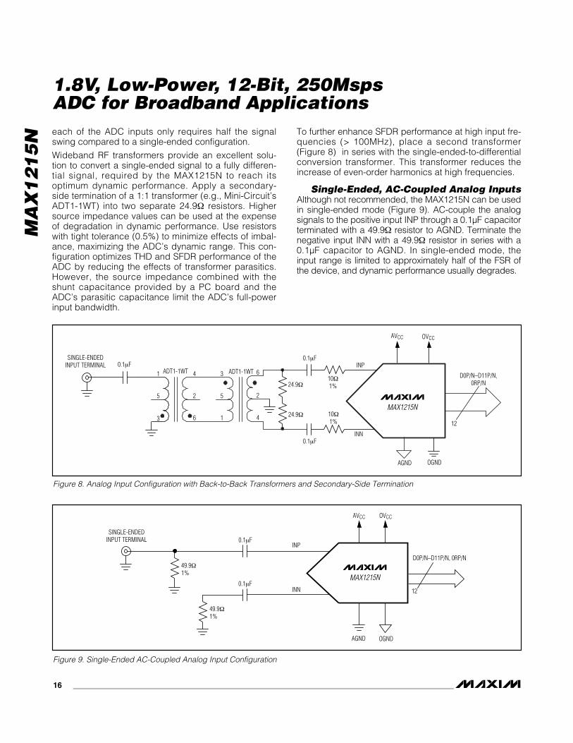
each of the ADC inputs only requires half the signalswing compared to a single-ended configuration.
Wideband RF transformers provide an excellent solu-tion to convert a single-ended signal to a fully differen-tial signal, required by the MAX1215N to reach itsoptimum dynamic performance. Apply a secondary-side termination of a 1:1 transformer (e.g., Mini-Circuit’sADT1-1WT) into two separate 24.9Ω resistors. Highersource impedance values can be used at the expenseof degradation in dynamic performance. Use resistorswith tight tolerance (0.5%) to minimize effects of imbal-ance, maximizing the ADC’s dynamic range. This con-figuration optimizes THD and SFDR performance of theADC by reducing the effects of transformer parasitics.However, the source impedance combined with theshunt capacitance provided by a PC board and theADC’s parasitic capacitance limit the ADC’s full-powerinput bandwidth.
To further enhance SFDR performance at high input fre-quencies (> 100MHz), place a second transformer(Figure 8) in series with the single-ended-to-differentialconversion transformer. This transformer reduces theincrease of even-order harmonics at high frequencies.
Single-Ended, AC-Coupled Analog InputsAlthough not recommended, the MAX1215N can be usedin single-ended mode (Figure 9). AC-couple the analogsignals to the positive input INP through a 0.1µF capacitorterminated with a 49.9Ω resistor to AGND. Terminate thenegative input INN with a 49.9Ω resistor in series with a0.1µF capacitor to AGND. In single-ended mode, theinput range is limited to approximately half of the FSR ofthe device, and dynamic performance usually degrades.
AGND OGND
D0P/N–D11P/N,0RP/N
AVCC
INP
INN
OVCC
12
MAX1215N
0.1µF
24.9Ω
24.9Ω
0.1µF1
5
3
4
2
6
3
5
1
6
2
4
ADT1-1WT ADT1-1WT10Ω1%
10Ω1%
0.1µFSINGLE-ENDEDINPUT TERMINAL
AGND OGND
D0P/N–D11P/N, 0RP/N
AVCC
INP
49.9Ω1%
49.9Ω1%
INN
OVCC
12
MAX1215N
0.1µFSINGLE-ENDED
INPUT TERMINAL
0.1µF
Figure 8. Analog Input Configuration with Back-to-Back Transformers and Secondary-Side Termination
Figure 9. Single-Ended AC-Coupled Analog Input Configuration

MA
X1
21
5N
1.8V, Low-Power, 12-Bit, 250Msps ADC for Broadband Applications
______________________________________________________________________________________ 17
Grounding, Bypassing, andBoard Layout Considerations
The MAX1215N requires board layout design tech-niques suitable for high-speed data converters. ThisADC provides separate analog and digital power sup-plies. The analog and digital supply voltage pinsaccept 1.7V to 1.9V input voltage ranges. Althoughboth supply types can be combined and supplied fromone source, it is recommended to use separate sourcesto cut down on performance degradation caused by dig-ital switching currents, which can couple into the analogsupply network. Isolate analog and digital supplies(AVCC and OVCC) where they enter the PC board withseparate networks of ferrite beads and capacitors totheir corresponding grounds (AGND, OGND).
To achieve optimum performance, provide each supplywith a separate network of a 47µF tantalum capacitorand parallel combinations of 10µF and 1µF ceramiccapacitors. Additionally, the ADC requires each supplypin to be bypassed with separate 0.1µF ceramiccapacitors (Figure 10). Locate these capacitors directlyat the ADC supply pins or as close as possible to theMAX1215N. Choose surface-mount capacitors, whosepreferred location should be on the same side as theconverter to save space and minimize the inductance.If close placement on the same side is not possible,these bypassing capacitors may be routed throughvias to the bottom side of the PC board.
Multilayer boards with separated ground and powerplanes produce the highest level of signal integrity.Consider the use of a split ground plane arranged to
match the physical location of analog and digitalground on the ADC’s package. The two ground planesshould be joined at a single point so the noisy digitalground currents do not interfere with the analog groundplane. The dynamic currents that may need to travellong distances before they are recombined at a com-mon-source ground, resulting in large and undesirableground loops, are a major concern with this approach.Ground loops can degrade the input noise by couplingback to the analog front-end of the converter, resultingin increased spurious activity, leading to decreasednoise performance.
Alternatively, all ground pins could share the sameground plane, if the ground plane is sufficiently isolatedfrom any noisy, digital systems ground. To minimize thecoupling of the digital output signals from the analoginput, segregate the digital output bus carefully from theanalog input circuitry. To further minimize the effects ofdigital noise coupling, ground return vias can be posi-tioned throughout the layout to divert digital switchingcurrents away from the sensitive analog sections of theADC. This approach does not require split groundplanes, but can be accomplished by placing substantialground connections between the analog front-end andthe digital outputs.
The MAX1215N is packaged in a 68-pin QFN-EP pack-age (package code: G6800-4), providing greaterdesign flexibility, increased thermal dissipation, andoptimized AC performance of the ADC. The exposedpaddle (EP) must be soldered down to AGND.
In this package, the data converter die is attached toan EP lead frame with the back of this frame exposed
AGND
NOTE: EACH POWER-SUPPLY PIN (ANALOG AND DIGITAL) SHOULD BE DECOUPLED WITH AN INDIVIDUAL 0.1µF CAPACITOR AS CLOSEAS POSSIBLE TO THE ADC.
BYPASSING—ADC LEVEL BYPASSING—BOARD LEVEL
ANALOG POWER-SUPPLY SOURCE
OGND
AGND OGND
D0P/N–D11P/N, 0RP/N
1µF 10µF0.1µF0.1µF
47µF
AVCC OVCC
12
MAX1215N
AVCC
DIGITAL/OUTPUTDRIVER POWER-SUPPLY SOURCE
1µF 10µF 47µF
OVCC
Figure 10. Grounding, Bypassing, and Decoupling Recommendations for the MAX1215N

MA
X1
21
5N
1.8V, Low-Power, 12-Bit, 250Msps ADC for Broadband Applications
18 _______________________________________________________________________________________
at the package bottom surface, facing the PC boardside of the package. This allows a solid attachment ofthe package to the board with standard infrared (IR)flow soldering techniques.
Thermal efficiency is one of the factors for selecting apackage with an exposed pad for the MAX1215N. Theexposed pad improves thermal efficiency and ensuresa solid ground connection between the ADC and thePC board’s analog ground layer.
Considerable care must be taken when routing the digi-tal output traces for a high-speed, high-resolution dataconverter. Keep trace lengths at a minimum and placeminimal capacitive loading (less than 5pF) on any digi-tal trace to prevent coupling to sensitive analog sec-tions of the ADC. It is recommended running the LVDSoutput traces as differential lines with 100Ω matchedimpedance from the ADC to the LVDS load device.
Static Parameter DefinitionsIntegral Nonlinearity (INL)
Integral nonlinearity is the deviation of the values on anactual transfer function from a straight line. This straightline can be either a best straight-line fit or a line drawnbetween the end points of the transfer function, once off-set and gain errors have been nullified. The static linearityparameters for the MAX1215N are measured using thehistogram method with a 10MHz input frequency.
Differential Nonlinearity (DNL)Differential nonlinearity is the difference between anactual step width and the ideal value of 1 LSB. A DNLerror specification of less than 1 LSB guarantees nomissing codes and a monotonic transfer function. TheMAX1215N’s DNL specification is measured with thehistogram method based on a 10MHz input tone.
Dynamic Parameter DefinitionsAperture Jitter
Figure 11 depicts the aperture jitter (tAJ), which is thesample-to-sample variation in the aperture delay.
Aperture DelayAperture delay (tAD) is the time defined between therising edge of the sampling clock and the instant whenan actual sample is taken (Figure 11).
Signal-to-Noise Ratio (SNR)For a waveform perfectly reconstructed from digital sam-ples, the theoretical maximum SNR is the ratio of the full-scale analog input (RMS value) to the RMS quantizationerror (residual error). The ideal, theoretical minimum ana-log-to-digital noise is caused by quantization error onlyand results directly from the ADC’s resolution (N bits):
SNR[max] = 6.02 x N + 1.76
In reality, other noise sources such as thermal noise,clock jitter, signal phase noise, and transfer functionnonlinearities are also contributing to the SNR calcula-tion and should be considered when determining thesignal-to-noise ratio in ADC.
Signal-to-Noise Plus Distortion (SINAD)SINAD is computed by taking the ratio of the RMS sig-nal to all spectral components excluding the fundamen-tal and the DC offset. In the case of the MAX1215N,SINAD is computed from a curve fit.
HOLD
ANALOGINPUT
SAMPLEDDATA (T/H)
T/H
tADtAJ
TRACK TRACK
CLKN
CLKP
Figure 11. Aperture Jitter/Delay Specifications

MA
X1
21
5N
1.8V, Low-Power, 12-Bit, 250Msps ADC for Broadband Applications
______________________________________________________________________________________ 19
Spurious-Free Dynamic Range (SFDR)SFDR is the ratio of RMS amplitude of the carrier fre-quency (maximum signal component) to the RMS valueof the next-largest noise or harmonic distortion compo-nent. SFDR is usually measured in dBc with respect tothe carrier frequency amplitude or in dBFS with respectto the ADC’s full-scale range.
Intermodulation Distortion (IMD)IMD is the ratio of the RMS sum of the intermodulationproducts to the RMS sum of the two fundamental inputtones. This is expressed as:
The fundamental input tone amplitudes (V1 and V2) are at-7dBFS. The intermodulation products are the amplitudesof the output spectrum at the following frequencies:
• Second-order intermodulation products: fIN1 + fIN2,fIN2 - fIN1
• Third-order intermodulation products: 2 x fIN1 - fIN2, 2 x fIN2 - fIN1, 2 x fIN1 + fIN2, 2 x fIN2 + fIN1
• Fourth-order intermodulation products: 3 x fIN1 - fIN2,3 x fIN2 - fIN1, 3 x fIN1 + fIN2, 3 x fIN2 + fIN1
• Fifth-order intermodulation products: 3 x fIN1 - 2 x fIN2,3 x fIN2 - 2 x fIN1, 3 x fIN1 + 2 x fIN2, 3 x fIN2 + 2 x fIN1
Full-Power BandwidthA large -1dBFS analog input signal is applied to anADC and the input frequency is swept up to the pointwhere the amplitude of the digitized conversion resulthas decreased by 3dB. The -3dB point is defined asthe full-power input bandwidth frequency of the ADC.
IMDV V V V
V V
IM IM IM IMn log......
= ×+ + + +
+
⎛
⎝
⎜⎜
⎞
⎠
⎟⎟
20 12
22
32 2
12
22
Pin Configuration
5859606162 5455565763
38
39
40
41
42
43
44
45
46
47
AVCC
AGND
AVCC
TOP VIEW
AVCC
OGND
OVCC
ORP
ORN
D11P
D11N
D10P
D10N
5253
D9P
D9N
AGND
AGND
AVCC
CLKN
CLKP
AVCC
AGND
OVCC
OGND D0
N
OVCC
D1N
D0P
D1P
D6P
D6N
OGND
OVCC
DCLKP
DCLKN
OVCC
D5P
D5N
D4P
35
36
37 D4N
D3P
D3N
AGND
INN
INP
AGND
AVCC
AGND
AGND
AVCC
AVCC
AVCC
AGND
REFADJ
REFIO
AGND
48 D7N
AVCC
64
AGND
656667
AGND
AGND
AVCC
68
T/B
2322212019 2726252418 2928 323130
D2N
D2P
3433
49
50 D8N
D7PEP
51 D8P
11
10
9
8
7
6
5
4
3
2
16
15
14
13
12
1
CLKDIV
EP = EXPOSED PADDLE.
17
MAX1215N
QFN

MA
X1
21
5N
1.8V, Low-Power, 12-Bit, 250Msps ADC for Broadband Applications
20 _______________________________________________________________________________________
68L
QFN
.EP
SC
1221-0122
PACKAGE OUTLINE, 68L QFN, 10x10x0.9 MM
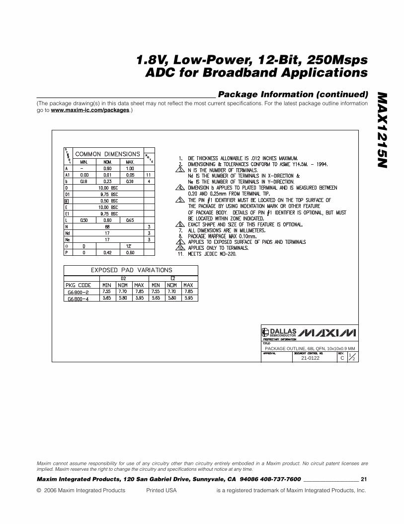
Package Information(The package drawing(s) in this data sheet may not reflect the most current specifications. For the latest package outline informationgo to www.maxim-ic.com/packages.)
For the MAX1215N, the package code is G6800-4.
MA
X1
21
5N
1.8V, Low-Power, 12-Bit, 250Msps ADC for Broadband Applications
Maxim cannot assume responsibility for use of any circuitry other than circuitry entirely embodied in a Maxim product. No circuit patent licenses areimplied. Maxim reserves the right to change the circuitry and specifications without notice at any time.
Maxim Integrated Products, 120 San Gabriel Drive, Sunnyvale, CA 94086 408-737-7600 ____________________ 21
© 2006 Maxim Integrated Products Printed USA is a registered trademark of Maxim Integrated Products, Inc.
Freed
C1
221-0122
PACKAGE OUTLINE, 68L QFN, 10x10x0.9 MM
Package Information (continued)(The package drawing(s) in this data sheet may not reflect the most current specifications. For the latest package outline informationgo to www.maxim-ic.com/packages.)


![MX29VS128F - Macronix 1.8V... · REVISION HISTORY ..... 63 5 P/N: PM1679 RE. 1.4, OCT. 21, 2015 MX29S128F 128M-BIT [8M x16-bit] CMOS 1.8 Volt, Multiplexed, Burst Mode Flash Memory](https://static.fdocuments.in/doc/165x107/6045adccc073a449d8513cfd/mx29vs128f-18v-revision-history-63-5-pn-pm1679-re-14-oct-21.jpg)