Evaluation Kit - Apex Microtechnology · 2019-10-29 · EK49 4 EK49U Rev A BEFORE YOU GET STARTED...
8
www.apexanalog.com © Apex Microtechnology Inc. All rights reserved Oct 2019 EK49U Rev A Evaluation Kit EK49 APPLICABLE PARTS (SOLD SEPARATELY) • MP165 INTRODUCTION This easy to use kit provides a platform with good circuit board layout and grounding to evaluate the MP165 Power Amplifier. The evaluation board provides options to install a load capacitor and series resistor to evaluate the MP165 performance with a printhead. All necessary components are provided with the kit. External connections to the evaluation kit can be made through the connectors at the edges of the circuit. The circuit provides a line termination of 50Ω. Figure 1: Circuit Configure Diagram OUT_2 GND +IN OUT_1 VTMP PDWN OCFLG -IN OUT MP165KL 16 15 14 13 12 11 10 9 8 7 6 5 4 3 2 1 17 18 19 20 N/C N/C N/C +VB +VS GND -VS -VB GND -VS ILIM+ -VB CC2 CC1 -IN +IN VTMP +VS +VB OCFLG ILIM- PDWN TP BB RING N/C GND +5V OUT TRX NC 21 N/C N/C Jumper on VB=VS Jumper on 22 23 N/C DUT VB=VS P2 P12 RT2 51 P10 P11 P15 P14 P13 P1 RT1 51 2 1 D3 400V 2 1 D4 400V TP12-1 TP11-1 CNF RN TP2-1 TP1-1 TP10-1 TP13-1 TP14-1 TP15-1 RIN1 2K RIN2 2K RFB1 49.9K RFB2 RISO RLIM 0.15 Ohm RS P8 P6 CBP2 470uF P7 TP8-1 TP6-1 TP7-1 P5 P3 CBP5 470uF TP3-1 TP5-1 P4 TP4-1 P17 P16 TP16-1 TP17-1 1 2 3 4 5 6 7 8 9 10 11 12 13 14 15 16 17 18 19 20 21 22 23 1 2 3 4 HS31 CFB1 X1 X2 RFB3 2 1 D1 2 1 D2 R1 2K CBP1 1uF C1 1uF 2 1 D6 18V 2 1 D5 18V CBP3 1uF CBP4 1uF CBP6 1uF 1 2 3 4 S1 SPST-N.O. CC2 3.3pF CC1 3.3pF TP21-1 TP22-1 X3 X4 -VS +VS +5V +5V +5V -VB -VS +VB +VS
Transcript of Evaluation Kit - Apex Microtechnology · 2019-10-29 · EK49 4 EK49U Rev A BEFORE YOU GET STARTED...

www.apexanalog.com © Apex Microtechnology Inc.All rights reserved
Oct 2019EK49U Rev A
Evaluation Kit
EK49
APPLICABLE PARTS (SOLD SEPARATELY) • MP165
INTRODUCTIONThis easy to use kit provides a platform with good circuit board layout and grounding to evaluate the
MP165 Power Amplifier. The evaluation board provides options to install a load capacitor and series resistorto evaluate the MP165 performance with a printhead. All necessary components are provided with the kit.External connections to the evaluation kit can be made through the connectors at the edges of the circuit.The circuit provides a line termination of 50Ω.
Figure 1: Circuit Configure Diagram
OUT_2
GND
+IN
OUT_1
VTMP
PDWN
OCFLG
-IN
OUTMP165KL
1615141312
11 10 9 8 7 6 5 4 3 2 1
17 18 19 20
N/C
N/C
N/C
+VB
+VS
GND
-VS
-VB
GND
-VS
ILIM+
-VB
CC2
CC1
-IN
+IN
VTMP
+VS+VB
OCF
LG
ILIM-
PDW
N
TP
BB R
ING
N/C
GND
+5V
OUT
TRX
NC
21
N/C
N/C
Jumper onVB=VS
Jumper on22 23
N/C
DUT
VB=VS
P2
P12
RT251
P10
P11
P15
P14
P13
P1
RT151
21
D3400V
21
D4400V
TP12-1
TP11-1
CNF
RN
TP2-1
TP1-1
TP10-1
TP13-1
TP14-1
TP15-1
RIN1
2K
RIN2
2K
RFB1
49.9K
RFB2
RISORLIM
0.15 Ohm
RS
P8
P6
CBP2470uF
P7
TP8-1
TP6-1
TP7-1
P5
P3
CBP5
470uF
TP3-1
TP5-1
P4TP4-1
P17
P16
TP16-1
TP17-1
1234567891011
12 13 14 15 16 17 18 19 20 21 22 23
1
2 3
4
HS31
CFB1
X1
X2
RFB3
21D1
2 1D2
R1
2K
CBP11uF
C11uF
21
D618V
21
D518V
CBP31uF
CBP41uF
CBP61uF
1
23
4
S1SPST-N.O.
CC23.3pF
CC13.3pF
TP21-1
TP22-1
X3
X4
-VS
+VS
+5V
+5V
+5V
-VB
-VS
+VB
+VS

EK49
2 EK49U Rev A
Figure 2: Circuit Board Layout

EK49
EK49U Rev A 3
PARTS LIST
Reference Manufacturer Part # Description QTY
ResistorsRT1, RT2 PR01000105109JR500 51Ω, 1W, 5% 2RIN1, RIN2 CMF552K0000FHEB 2kΩ, 1/2W, 1% 2RFB1 CMF5549K900FHEB 49.9kΩ, 1/2W, 1% 2RLIM 15FR150E 0.15Ω, 5W, 1% 1DiodesD1, D2 1N4148TR Diode, General Purpose 2D3, D4 MUR440G TVS diode, 400V 2D5, D6 1N5931BRLG Zener Diode, 18V 2CapacitorsC1, CBP1, CBP3, CBP4, CBP6 C5750X7R2E105K230KA 1µF, 250V, Film Cap 5CBP2, CBP5 KMH450VN471M35X50T2 470µF, 450V, Electrolytic Cap 2CC1, CC2 561R10TCCV33BA 3.3pF, 1kV, Ceramic Cap 2Hardware
HS31 Heatsink for Amplifier 1
MS11 Cage Jacks for Amplifier 1
146510CJ BNC Connector 2571-0100 Banana jacks, pc mount 1491735A190 Screw Pan head, #8 490272A105 Screw Pan head, #4 294997A350 Screw, Round head, #8 42221 Standoff, hex, #8 45007 Test Points 20SPC02SVJN-RC Jumper, Slip On 10PRPC002SADN-RC Header, Connector 10
MiscellaneousS1 VQ-PAC07K SPST Push button Switch 1

EK49
4 EK49U Rev A
BEFORE YOU GET STARTED• All Apex Microtechnology amplifiers should be handled using proper ESD precautions. • Always use the heatsink included in this kit. • Always use adequate power supply bypassing. • Do not change the connections while the circuit is powered. • Initially set all power supplies to the minimum operation levels allowed on the device data sheet. • Check for oscillations. • Please refer to Application Note, AN01 for general operating conditions.
ASSEMBLY INSTRUCTIONSDuring the assembly, please refer to the circuit schematics, assembly drawings, and the data sheet of the
part being used on the evaluation kit.
1. Note that each side of the circuit board is identified as either the component side or the DUT side. The component side has the designators printed on that side.
2. All through hole components (except the cage jacks) are installed on the component side of the board and soldered on the DUT side.
3. A pin receptacle is supplied with this evaluation kit. Break it into two strips 11 and 12 pins long. Insert the carrier strip through the DUT side and solder the cage jacks on the component side. Once the cage jacks are soldered, remove the carrier strip, leaving only cage jacks soldered on the board.
4. Install C1, CBP1, CBP3, CBP4, CBP6, CC1 and CC2 on the component side of the board. 5. Install in X1, X2, X3 and X4.6. Next, install all the smaller components on the board. This is done because it becomes difficult to install a
small part on the board once all the larger components are installed.7. Install diodes and capacitors CBP2 and CBP5 on the component side of the board. Ensure that the orienta-
tion of the components match the circuit schematic drawing.8. Mount the BNC connector provided with the kit (146510CJ) and solder it to the board. Also mount the
banana jacks on the board. Install other miscellaneous components like test points and S1 switch to com-plete your application circuit.
9. From the DUT side of the PCB, snap the spacer-grommets into the holes at the four corners of the PCB. Notice that the holes are slightly rectangular and match the spacer-grommets long and short sides to the holes in the PCB.
10. Apply a thin, uniform layer of thermal grease to the amplifier; a straight edge may be useful here. Position the amplifier over the mounting holes in the heatsink. Firmly push the amplifier onto the heatsink while slightly rotating the amplifier back and forth, ending with the mounting holes of the amplifier over the mounting holes in the heatsink.
11. Use 4-40x¼' machine screws to mount the amplifier to the heatsink. Do not over-tighten the screws as this provides no thermal benefit and may break the hardware.
12. Carefully lower the PCB assembly until the pins of the amplifier engage the cage jacks and then continue pushing the PCB assembly in the area between the amplifier's pins until the four spacer grommets at the four corners of the PCB touch the heatsink. At this point the PCB should not be bowed.
13. Use #8 sheet metal screws to mount the PCB to the heat sink at the four spacer-grommets.14. #8 hex stand offs (91841A009) are also provided with the kit. Install the # 8 x 0.375"screws (91735A190),
provided with the kit, from the component side. Attach the standoffs to these screws on the corners of the board. Refer to the assembly drawings while installing the standoffs.
EK49
EK49U Rev A 5
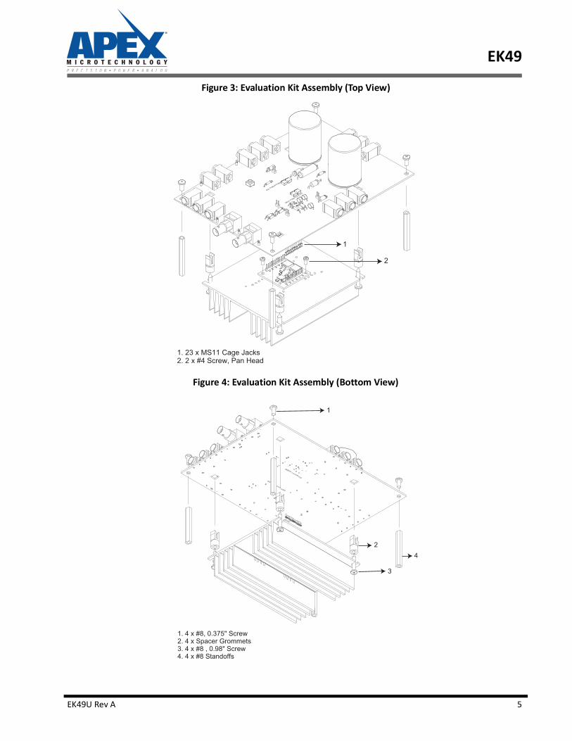
Figure 3: Evaluation Kit Assembly (Top View)
Figure 4: Evaluation Kit Assembly (Bottom View)
1
2
1. 23 x MS11 Cage Jacks2. 2 x #4 Screw, Pan Head
1
2
3
4
1. 4 x #8, 0.375" Screw2. 4 x Spacer Grommets3. 4 x #8 , 0.98" Screw4. 4 x #8 Standoffs

EK49
6 EK49U Rev A
TEST ASSEMBLY EQUIPMENT NEEDED1. High Voltage Power Supply2. Function Generators for PWM input or a microcontroller3. Oscilloscope4. Heatsink
TEST SETUPConnect the power supply to +VS and -VS ports. If you wish to use boost supply, connect boost voltage
supplies to +VB and -VB ports. Otherwise, short +VS to +VB and -VS or -VB. Refer to the product data sheet forvoltage specifications. Connect the BNC cable from the function generator to either P1 port for inverting con-figuration or to P2 for non-inverting configuration. Connect a 5V DC supply to P16 port for over current flag.
Do not plug in the MP165 yet. Now power on the input signal and power supplies. Measure voltages onall cage jacks on the DUT side to ensure that there is no short and to check if all the pins (cage jacks) read cor-rect voltages.
Now, mount the MP165 on EVAL 92. If connecting a resistor load, connect between ports P11 and P10.Input and output waveforms can be checked on an Oscilloscope by connecting it to the test points mountedon the board. Begin the test with minimum values of input and supply voltages.
Figure 5 and 6 show the input, output and over current flag waveforms when a MP165 is evaluated usingthe EK49 evaluation kit. The yellow waveform (channel 1) represents an input signal of 4VP-P and the cyanwaveform (channel 2) represents an output signal of 100VP-P. The magenta waveform (channel 3) representsthe over current flag.
During normal operation, the over current flag will remain high as shown in figure 5. When the amplifierstarts operating in current limit mode, the over current flag becomes low as shown in figure 6.

EK49
EK49U Rev A 7
Figure 5: Normal Operation
Figure 6: Current Limit Operation

EK49
8 EK49U Rev A
NEED TECHNICAL HELP? CONTACT APEX SUPPORT! For all Apex Microtechnology product questions and inquiries, call toll free 800-546-2739 in North America. Forinquiries via email, please contact [email protected]. International customers can also requestsupport by contacting their local Apex Microtechnology Sales Representative. To find the one nearest to you,go to www.apexanalog.com
IMPORTANT NOTICE
Apex Microtechnology, Inc. has made every effort to insure the accuracy of the content contained in this document. However, the information issubject to change without notice and is provided "AS IS" without warranty of any kind (expressed or implied). Apex Microtechnology reserves the rightto make changes without further notice to any specifications or products mentioned herein to improve reliability. This document is the property ofApex Microtechnology and by furnishing this information, Apex Microtechnology grants no license, expressed or implied under any patents, maskwork rights, copyrights, trademarks, trade secrets or other intellectual property rights. Apex Microtechnology owns the copyrights associated with theinformation contained herein and gives consent for copies to be made of the information only for use within your organization with respect to ApexMicrotechnology integrated circuits or other products of Apex Microtechnology. This consent does not extend to other copying such as copying forgeneral distribution, advertising or promotional purposes, or for creating any work for resale. APEX MICROTECHNOLOGY PRODUCTS ARE NOT DESIGNED, AUTHORIZED OR WARRANTED TO BE SUITABLE FOR USE IN PRODUCTS USED FOR LIFESUPPORT, AUTOMOTIVE SAFETY, SECURITY DEVICES, OR OTHER CRITICAL APPLICATIONS. PRODUCTS IN SUCH APPLICATIONS ARE UNDERSTOOD TO BEFULLY AT THE CUSTOMER OR THE CUSTOMER’S RISK. Apex Microtechnology, Apex and Apex Precision Power are trademarks of Apex Microtechnology, Inc. All other corporate names noted herein may betrademarks of their respective holders.