EVALUATION KIT 10-Bit, 7.5Msps, Ultra-Low-Power … · dac3 dd cs sclk din t/r dout shdn thin qfn...
37
General Description The MAX19705 is an ultra-low-power, mixed-signal ana- log front-end (AFE) designed for power-sensitive com- munication equipment. Optimized for high dynamic performance at ultra-low power, the device integrates a dual 10-bit, 7.5Msps receive (Rx) ADC; dual 10-bit, 7.5Msps transmit (Tx) DAC; three fast-settling 12-bit aux-DAC channels for ancillary RF front-end control; and a 10-bit, 333ksps housekeeping aux-ADC. The typ- ical operating power in Tx-Rx FAST mode is 28.2mW at a 7.5MHz clock frequency. The Rx ADCs feature 55.1dB SNR and 73.4dBc SFDR at a 1.875MHz input frequency with a 7.5MHz clock fre- quency. The analog I/Q input amplifiers are fully differen- tial and accept 1.024V P-P full-scale signals. Typical I/Q channel matching is ±0.01° phase and ±0.02dB gain. The Tx DACs feature 77.2dBc SFDR at f OUT = 620kHz and f CLK = 7.5MHz. The analog I/Q full-scale output voltage is ±400mV differential. The Tx DAC common- mode DC level is programmable from 0.9V to 1.35V. The I/Q channel offset is adjustable. The typical I/Q channel matching is ±0.03dB gain and ±0.08° phase. The Rx ADC and Tx DAC share a single, 10-bit parallel, high-speed digital bus allowing half-duplex operation for time-division duplex (TDD) applications. A 3-wire serial interface controls power-management modes, the aux-DAC channels, and the aux-ADC channels. The MAX19705 operates on a single +2.7V to +3.3V analog supply and +1.8V to +3.3V digital I/O supply. The MAX19705 is specified for the extended (-40°C to +85°C) temperature range and is available in a 48-pin, thin QFN package. The Selector Guide at the end of the data sheet lists other pin-compatible versions in this AFE family. Applications Broadband Access Radio Private Mobile Radio (PMR) Portable Communication Equipment Features ♦ Dual 10-Bit, 7.5Msps Rx ADC and Dual 10-Bit, 7.5Msps Tx DAC ♦ Ultra-Low Power 28.2mW at f CLK = 7.5MHz, Fast Mode 21mW at f CLK = 7.5MHz, Slow Mode Low-Current Standby and Shutdown Modes ♦ Programmable Tx DAC Common-Mode DC Level and I/Q Offset Trim ♦ Excellent Dynamic Performance SNR = 55.1dB at f IN = 1.875MHz (Rx ADC) SFDR = 77.2dBc at f OUT = 620kHz (Tx DAC) ♦ Three 12-Bit, 1μs Aux-DACs ♦ 10-Bit, 333ksps Aux-ADC with 4:1 Input Mux and Data Averaging ♦ Excellent Gain/Phase Match ±0.01° Phase, ±0.02dB Gain (Rx ADC) at f IN = 1.875MHz ♦ Multiplexed Parallel Digital I/O ♦ Serial-Interface Control ♦ Versatile Power-Control Circuits Shutdown, Standby, Idle, Tx/Rx Disable ♦ Miniature 48-Pin Thin QFN Package (7mm x 7mm x 0.8mm) MAX19705 10-Bit, 7.5Msps, Ultra-Low-Power Analog Front-End ________________________________________________________________ Maxim Integrated Products 1 19-3763; Rev 0; 8/05 For pricing, delivery, and ordering information, please contact Maxim/Dallas Direct! at 1-888-629-4642, or visit Maxim’s website at www.maxim-ic.com. EVALUATION KIT AVAILABLE Ordering Information PART* PIN-PACKAGE PKG CODE MAX19705ETM 48 Thin QFN-EP** T4877-4 MAX19705ETM+ 48 Thin QFN-EP** T4877-4 *All devices are specified over the -40°C to +85°C operating range. **EP = Exposed paddle. +Denotes lead-free package. Functional Diagram and Selector Guide appear at end of data sheet. D9 D8 D6 OV DD D4 D3 D2 D0 D1 OGND D5 D7 V DD IDN IDP GND V DD QDN QDP REFN EXPOSED PADDLE (GND) REFIN DAC1 COM DAC2 37 38 39 40 41 42 43 44 45 46 47 48 1 2 3 4 5 6 7 8 9 10 24 23 22 21 20 19 18 17 16 15 14 13 ADC1 ADC2 V DD GND V DD CS SCLK DIN T/R SHDN DOUT DAC3 THIN QFN MAX19705 TOP VIEW REFP V DD IAP IAN GND CLK GND V DD QAN QAP V DD GND 11 12 36 35 34 33 32 31 30 29 28 27 26 25 Pin Configuration
Transcript of EVALUATION KIT 10-Bit, 7.5Msps, Ultra-Low-Power … · dac3 dd cs sclk din t/r dout shdn thin qfn...

General DescriptionThe MAX19705 is an ultra-low-power, mixed-signal ana-log front-end (AFE) designed for power-sensitive com-munication equipment. Optimized for high dynamicperformance at ultra-low power, the device integrates adual 10-bit, 7.5Msps receive (Rx) ADC; dual 10-bit,7.5Msps transmit (Tx) DAC; three fast-settling 12-bitaux-DAC channels for ancillary RF front-end control;and a 10-bit, 333ksps housekeeping aux-ADC. The typ-ical operating power in Tx-Rx FAST mode is 28.2mW ata 7.5MHz clock frequency.
The Rx ADCs feature 55.1dB SNR and 73.4dBc SFDR ata 1.875MHz input frequency with a 7.5MHz clock fre-quency. The analog I/Q input amplifiers are fully differen-tial and accept 1.024VP-P full-scale signals. Typical I/Qchannel matching is ±0.01° phase and ±0.02dB gain.
The Tx DACs feature 77.2dBc SFDR at fOUT = 620kHzand fCLK = 7.5MHz. The analog I/Q full-scale outputvoltage is ±400mV differential. The Tx DAC common-mode DC level is programmable from 0.9V to 1.35V.The I/Q channel offset is adjustable. The typical I/Qchannel matching is ±0.03dB gain and ±0.08° phase.
The Rx ADC and Tx DAC share a single, 10-bit parallel,high-speed digital bus allowing half-duplex operationfor time-division duplex (TDD) applications. A 3-wireserial interface controls power-management modes, theaux-DAC channels, and the aux-ADC channels.
The MAX19705 operates on a single +2.7V to +3.3Vanalog supply and +1.8V to +3.3V digital I/O supply.The MAX19705 is specified for the extended (-40°C to+85°C) temperature range and is available in a 48-pin,thin QFN package. The Selector Guide at the end of thedata sheet lists other pin-compatible versions in thisAFE family.
ApplicationsBroadband Access Radio
Private Mobile Radio (PMR)
Portable Communication Equipment
Features♦ Dual 10-Bit, 7.5Msps Rx ADC and Dual 10-Bit,
7.5Msps Tx DAC
♦ Ultra-Low Power28.2mW at fCLK = 7.5MHz, Fast Mode21mW at fCLK = 7.5MHz, Slow ModeLow-Current Standby and Shutdown Modes
♦ Programmable Tx DAC Common-Mode DC Leveland I/Q Offset Trim
♦ Excellent Dynamic PerformanceSNR = 55.1dB at fIN = 1.875MHz (Rx ADC)SFDR = 77.2dBc at fOUT = 620kHz (Tx DAC)
♦ Three 12-Bit, 1µs Aux-DACs
♦ 10-Bit, 333ksps Aux-ADC with 4:1 Input Mux andData Averaging
♦ Excellent Gain/Phase Match±0.01° Phase, ±0.02dB Gain (Rx ADC) at fIN = 1.875MHz
♦ Multiplexed Parallel Digital I/O
♦ Serial-Interface Control
♦ Versatile Power-Control CircuitsShutdown, Standby, Idle, Tx/Rx Disable
♦ Miniature 48-Pin Thin QFN Package (7mm x 7mm x 0.8mm)
MA
X1
97
05
10-Bit, 7.5Msps, Ultra-Low-PowerAnalog Front-End
________________________________________________________________ Maxim Integrated Products 1
19-3763; Rev 0; 8/05
For pricing, delivery, and ordering information, please contact Maxim/Dallas Direct! at 1-888-629-4642, or visit Maxim’s website at www.maxim-ic.com.
EVALUATION KIT
AVAILABLE
Ordering Information
PART* PIN-PACKAGE PKG CODE
MAX19705ETM 48 Thin QFN-EP** T4877-4
MAX19705ETM+ 48 Thin QFN-EP** T4877-4
*All devices are specified over the -40°C to +85°C operatingrange.**EP = Exposed paddle.+Denotes lead-free package.
Functional Diagram and Selector Guide appear at end ofdata sheet.
D9D8
D6OVDD
D4
D3D2
D0D1
OGNDD5
D7VDD
IDNIDP
GND
VDD
QDNQDP
REFN
EXPOSED PADDLE (GND)REFIN
DAC1
COM
DAC2 37
38
39
40
41
42
43
44
45
46
47
48
1 2 3 4 5 6 7 8 9 10
24
23
22
21
20
19
18
17
16
15
14
13
ADC1
ADC2
V DD
GND
V DD
CS SCLK
DIN
T/R
SHDN
DOUT
DAC3
THIN QFN
MAX19705
TOP VIEW
REFP V D
D
IAP
IAN
GND
CLK
GND
V DD
QAN
QAP
V DD
GND
11 12
36 35 34 33 32 31 30 29 28 27 26 25
Pin Configuration

MA
X1
97
05
10-Bit, 7.5Msps, Ultra-Low-PowerAnalog Front-End
2 _______________________________________________________________________________________
ABSOLUTE MAXIMUM RATINGS
Stresses beyond those listed under “Absolute Maximum Ratings” may cause permanent damage to the device. These are stress ratings only, and functionaloperation of the device at these or any other conditions beyond those indicated in the operational sections of the specifications is not implied. Exposure toabsolute maximum rating conditions for extended periods may affect device reliability.
VDD to GND, OVDD to OGND ..............................-0.3V to +3.6VGND to OGND.......................................................-0.3V to +0.3VIAP, IAN, QAP, QAN, IDP, IDN, QDP,
QDN, DAC1, DAC2, DAC3 to GND.....................-0.3V to VDDADC1, ADC2 to GND.................................-0.3V to (VDD + 0.3V)REFP, REFN, REFIN, COM to GND ...........-0.3V to (VDD + 0.3V)D0–D9, DOUT, T/R, SHDN, SCLK, DIN, CS,
CLK to OGND .....................................-0.3V to (OVDD + 0.3V)
Continuous Power Dissipation (TA = +70°C)48-Pin Thin QFN (derate 27.8mW/°C above +70°C) .....2.22W
Thermal Resistance θJA ..................................................36°C/WOperating Temperature Range ...........................-40°C to +85°CJunction Temperature ......................................................+150°CStorage Temperature Range .............................-60°C to +150°CLead Temperature (soldering, 10s) .................................+300°C
ELECTRICAL CHARACTERISTICS(VDD = 3V, OVDD = 1.8V, internal reference (1.024V), CL ≈ 10pF on all digital outputs, fCLK = 7.5MHz (50% duty cycle), Rx ADC inputamplitude = -0.5dBFS, Tx DAC output amplitude = 0dBFS, differential Rx ADC input, differential Tx DAC output, CREFP = CREFN =CCOM = 0.33µF, unless otherwise noted. CL < 5pF on all aux-DAC outputs. Typical values are at TA = +25°C.) (Note 1)
PARAMETER SYMBOL CONDITIONS MIN TYP MAX UNITS
POWER REQUIREMENTS
Analog Supply Voltage VDD 2.7 3.0 3.3 V
Output Supply Voltage OVDD 1.8 VDD V
Ext1-Tx, Ext3-Tx, and SPI2-Tx states;transmit DAC operating mode (Tx):fCLK = 7.5MHz, fOUT = 620kHz on bothchannels; aux-DACs ON and at midscale,aux-ADC ON
7.4
Ext2-Tx, Ext4-Tx, and SPI4-Tx states;transmit DAC operating mode (Tx):fCLK = 7.5MHz, fOUT = 620kHz on bothchannels; aux-DACs ON and at midscale,aux-ADC ON
9.6 12.5
Ext1-Rx, Ext4-Rx, and SPI3-Rx states;receive ADC operating mode (Rx):fCLK = 7.5MHz, fIN = 1.875MHz on bothchannels; aux-DACs ON and at midscale,aux-ADC ON
9.4 11
VDD Supply Current
Ext2-Rx, Ext3-Rx, and SPI1-Rx states;receive ADC operating mode (Rx):fCLK = 7.5MHz, fIN = 1.875MHz on bothchannels; aux-DACs ON and at midscale,aux-ADC ON
7
mA

MA
X1
97
05
10-Bit, 7.5Msps, Ultra-Low-PowerAnalog Front-End
_______________________________________________________________________________________ 3
ELECTRICAL CHARACTERISTICS (continued)(VDD = 3V, OVDD = 1.8V, internal reference (1.024V), CL ≈ 10pF on all digital outputs, fCLK = 7.5MHz (50% duty cycle), Rx ADC inputamplitude = -0.5dBFS, Tx DAC output amplitude = 0dBFS, differential Rx ADC input, differential Tx DAC output, CREFP = CREFN =CCOM = 0.33µF, unless otherwise noted. CL < 5pF on all aux-DAC outputs. Typical values are at TA = +25°C.) (Note 1)
PARAMETER SYMBOL CONDITIONS MIN TYP MAX UNITS
Standby mode: CLK = 0 or OVDD;aux-DACs ON and at midscale,aux-ADC ON
2.9 3.5
Idle mode: fCLK = 7.5MHz; aux-DACs ONand at midscale, aux-ADC ON
4.7 6
mAVDD Supply Current
Shutdown mode: CLK = 0 or OVDD 0.6 µA
Ext1-Rx, Ext2-Rx, Ext3-Rx, Ext4-Rx,SPI1-Rx, SPI3-Rx states; receive ADCoperating mode (Rx): fCLK = 7.5MHz,fIN = 1.875MHz on both channels;aux-DACs ON and at midscale,aux-ADC ON
1.4 mA
Ext1-Tx, Ext2-Tx, Ext3-Tx, Ext4-Tx,SPI2-Tx, SPI4-Tx states; transmit DACoperating mode (Tx): fCLK = 7.5MHz, fOUT= 620kHz on both channels; aux-DACsON and at midscale, aux-ADC ON
69
Standby mode: CLK = 0 or OVDD; aux-DACs ON and at midscale, aux-ADC ON
1
Idle mode: fCLK = 7.5MHz; aux-DACs ONand at midscale, aux-ADC ON
13.8
OVDD Supply Current
Shutdown mode: CLK = 0 or OVDD 0.01
µA
Rx ADC DC ACCURACY
Resolution N 10 Bits
Integral Nonlinearity INL ±0.6 LSB
Differential Nonlinearity DNL Guar anteed no m i ssi ng cod e ( N ote 2) -1 ±0.4 +1 LSB
Offset Error Residual DC offset error -5.5 ±0.4 +5.5 %FS
Gain Error Include reference error -8 ±1.65 +11 %FS
DC Gain Matching -0.25 ±0.01 +0.25 dB
Offset Matching ±12 LSB
Gain Temperature Coefficient ±13 ppm/°C
Offset error (VDD ±5%) ±1.7 LSBPower-Supply Rejection PSRR
Gain error (VDD ±5%) ±0.05 %FS

MA
X1
97
05
10-Bit, 7.5Msps, Ultra-Low-PowerAnalog Front-End
4 _______________________________________________________________________________________
ELECTRICAL CHARACTERISTICS (continued)(VDD = 3V, OVDD = 1.8V, internal reference (1.024V), CL ≈ 10pF on all digital outputs, fCLK = 7.5MHz (50% duty cycle), Rx ADC inputamplitude = -0.5dBFS, Tx DAC output amplitude = 0dBFS, differential Rx ADC input, differential Tx DAC output, CREFP = CREFN =CCOM = 0.33µF, unless otherwise noted. CL < 5pF on all aux-DAC outputs. Typical values are at TA = +25°C.) (Note 1)
PARAMETER SYMBOL CONDITIONS MIN TYP MAX UNITS
Rx ADC ANALOG INPUT
Input Differential Range VID Differential or single-ended inputs ±0.512 V
Input Common-Mode VoltageRange
VCM VDD / 2 V
RIN Switched capacitor load 720 kΩInput Impedance
CIN 5 pF
Rx ADC CONVERSION RATE
Maximum Clock Frequency fCLK (Note 3) 7.5 MHz
Channel I 5Data Latency (Figure 3)
Channel Q 5.5ClockCycles
Rx ADC DYNAMIC CHARACTERISTICS (Note 4)
fIN = 1.875MHz, fCLK = 7.5MHz 53.7 55.1Signal-to-Noise Ratio SNR
fIN = 3.5MHz, fCLK = 7.5MHz 55.1dB
fIN = 1.875MHz, fCLK = 7.5MHz 53.6 55Signal-to-Noise and Distortion SINAD
fIN = 3.5MHz, fCLK = 7.5MHz 55dB
fIN = 1.875MHz, fCLK = 7.5MHz 64 73.4Spurious-Free Dynamic Range SFDR
fIN = 3.5MHz, fCLK = 7.5MHz 74dBc
fIN = 1.875MHz, fCLK = 7.5MHz -84.5Third-Harmonic Distortion HD3
fIN = 3.5MHz, fCLK = 7.5MHz -82.5dBc
Intermodulation Distortion IMDf1 = 1.8MHz, -7dBFS;f2 = 1.0MHz, -7dBFS
-69.5 dBc
Third-Order IntermodulationDistortion
IM3f1 = 1.8MHz, -7dBFS;f2 = 1.0MHz, -7dBFS
-78.1 dBc
fIN = 1.875MHz, fCLK = 7.5MHz -71.9 -62.5Total Harmonic Distortion THD
fIN = 3.5MHz, fCLK = 7.5MHz -72dB
Aperture Delay 3.5 ns
Overdrive Recovery Time 1.5x full-scale input 2 ns
Rx ADC INTERCHANNEL CHARACTERISTICS
Crosstalk RejectionfIN X ,Y = 1.875M H z at - 0.5d BFS , fIN X ,Y = 1M H zat - 0.5d BFS ( N ote 5)
-91.5 dB
Amplitude Matching fIN = 1.875MHz at -0.5dBFS (Note 6) ±0.02 dB
Phase Matching fIN = 1.875MHz at -0.5dBFS (Note 6) ±0.01 D eg r ees
MA
X1
97
05
10-Bit, 7.5Msps, Ultra-Low-PowerAnalog Front-End
_______________________________________________________________________________________ 5
ELECTRICAL CHARACTERISTICS (continued)(VDD = 3V, OVDD = 1.8V, internal reference (1.024V), CL ≈ 10pF on all digital outputs, fCLK = 7.5MHz (50% duty cycle), Rx ADC inputamplitude = -0.5dBFS, Tx DAC output amplitude = 0dBFS, differential Rx ADC input, differential Tx DAC output, CREFP = CREFN =CCOM = 0.33µF, unless otherwise noted. CL < 5pF on all aux-DAC outputs. Typical values are at TA = +25°C.) (Note 1)
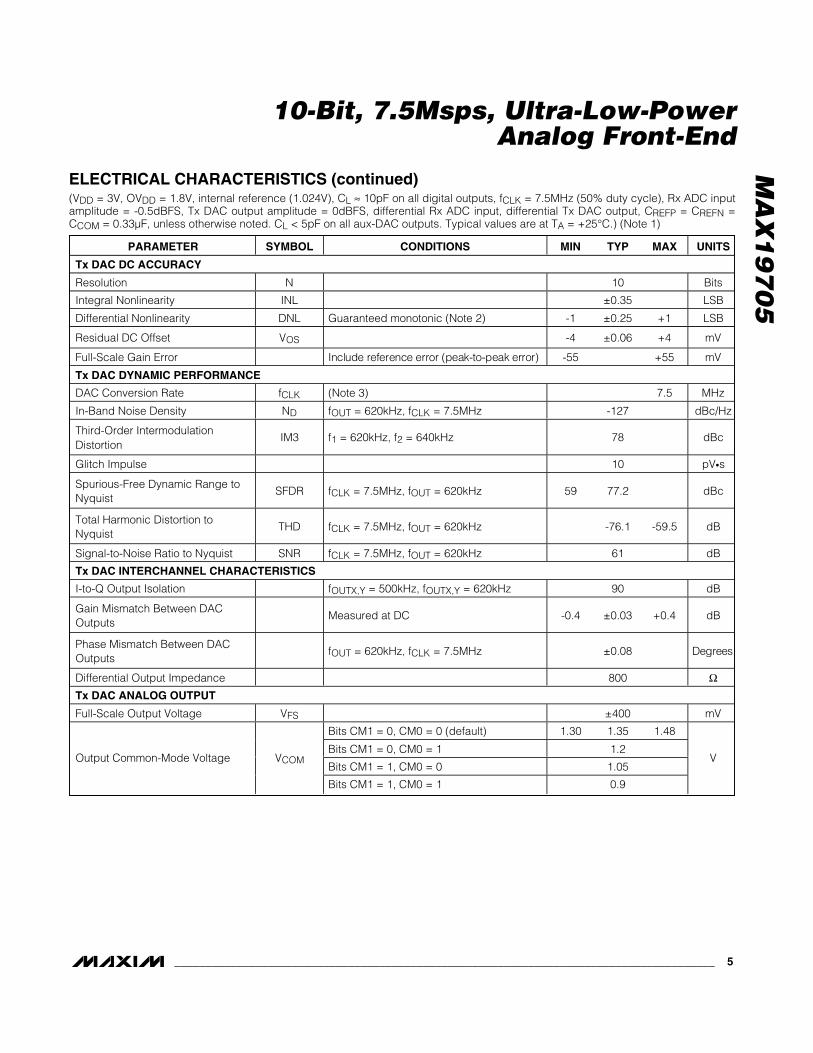
PARAMETER SYMBOL CONDITIONS MIN TYP MAX UNITS
Tx DAC DC ACCURACY
Resolution N 10 Bits
Integral Nonlinearity INL ±0.35 LSB
Differential Nonlinearity DNL Guaranteed monotonic (Note 2) -1 ±0.25 +1 LSB
Residual DC Offset VOS -4 ±0.06 +4 mV
Full-Scale Gain Error Incl ud e r efer ence er r or ( p eak- to- p eak er r or ) -55 +55 mV
Tx DAC DYNAMIC PERFORMANCE
DAC Conversion Rate fCLK (Note 3) 7.5 MHz
In-Band Noise Density ND fOUT = 620kHz, fCLK = 7.5MHz -127 dBc/Hz
Third-Order IntermodulationDistortion
IM3 f1 = 620kHz, f2 = 640kHz 78 dBc
Glitch Impulse 10 pV•s
Spurious-Free Dynamic Range toNyquist
SFDR fCLK = 7.5MHz, fOUT = 620kHz 59 77.2 dBc
Total Harmonic Distortion toNyquist
THD fCLK = 7.5MHz, fOUT = 620kHz -76.1 -59.5 dB
Signal-to-Noise Ratio to Nyquist SNR fCLK = 7.5MHz, fOUT = 620kHz 61 dB
Tx DAC INTERCHANNEL CHARACTERISTICS
I-to-Q Output Isolation fOUTX,Y = 500kHz, fOUTX,Y = 620kHz 90 dB
Gain Mismatch Between DACOutputs
Measured at DC -0.4 ±0.03 +0.4 dB
Phase Mismatch Between DACOutputs
fOUT = 620kHz, fCLK = 7.5MHz ±0.08 D eg r ees
Differential Output Impedance 800 ΩTx DAC ANALOG OUTPUT
Full-Scale Output Voltage VFS ±400 mV
Bits CM1 = 0, CM0 = 0 (default) 1.30 1.35 1.48
Bits CM1 = 0, CM0 = 1 1.2
Bits CM1 = 1, CM0 = 0 1.05Output Common-Mode Voltage VCOM
Bits CM1 = 1, CM0 = 1 0.9
V

MA
X1
97
05
10-Bit, 7.5Msps, Ultra-Low-PowerAnalog Front-End
6 _______________________________________________________________________________________
ELECTRICAL CHARACTERISTICS (continued)(VDD = 3V, OVDD = 1.8V, internal reference (1.024V), CL ≈ 10pF on all digital outputs, fCLK = 7.5MHz (50% duty cycle), Rx ADC inputamplitude = -0.5dBFS, Tx DAC output amplitude = 0dBFS, differential Rx ADC input, differential Tx DAC output, CREFP = CREFN =CCOM = 0.33µF, unless otherwise noted. CL < 5pF on all aux-DAC outputs. Typical values are at TA = +25°C.) (Note 1)
PARAMETER SYMBOL CONDITIONS MIN TYP MAX UNITS
Rx ADC–Tx DAC INTERCHANNEL CHARACTERISTICS
Receive Transmit IsolationADC fINI = fINQ = 1.875MHz, DAC fOUTI =fOUTQ = 620kHz, fCLK = 7.5MHz
90 dB
AUXILIARY ADC (ADC1, ADC2)Resolution N 10 Bits
AD1 = 0 (default) 2.048Full-Scale Reference VREF
AD1 = 1 VDDV
Analog Input Range0 toVREF
V
Analog Input Impedance At DC 500 kΩ
Input-Leakage CurrentMeasured at unselected input from 0 toVREF
±0.1 µA
Gain Error GE Includes reference error -5 +5 %FS
Zero-Code Error ZE 2 mV
Differential Nonlinearity DNL ±0.53 LSB
Integral Nonlinearity INL ±0.45 LSB
Supply Current 210 µA
AUXILIARY DACs (DAC1, DAC2, DAC3)
Resolution N (Note 2) 12 Bits
Integral Nonlinearity INL ±1.25 LSB
Differential Nonlinearity DNLGuaranteed monotonic over codes 100 to4000 (Note 2)
-1.0 ±0.65 +1.2 LSB
Gain Error GE RL > 200kΩ ±0.7 %FS
Zero-Code Error ZE ±0.6 %FS
Output-Voltage Low VOL RL > 200kΩ 0.1 V
Output-Voltage High VOH RL > 200kΩ 2.56 V
DC Output Impedance DC output at midscale 4 ΩSettling Time From 1/4 FS to 3/4 FS, within ±10 LSB 1 µs
Glitch Impulse From 0 to FS transition 24 nV•s
Rx ADC-Tx DAC TIMING CHARACTERISTICS
CLK Rise to Channel-I Output DataValid
tDOI Figure 3 (Note 2) 5.0 6.7 8.5 ns
CLK Fall to Channel-Q OutputData Valid
tDOQ Figure 3 (Note 2) 7.0 8.9 11.3 ns
I-DAC DATA to CLK Fall SetupTime
tDSI Figure 5 (Note 2) 10 ns

MA
X1
97
05
10-Bit, 7.5Msps, Ultra-Low-PowerAnalog Front-End
_______________________________________________________________________________________ 7
ELECTRICAL CHARACTERISTICS (continued)(VDD = 3V, OVDD = 1.8V, internal reference (1.024V), CL ≈ 10pF on all digital outputs, fCLK = 7.5MHz (50% duty cycle), Rx ADC inputamplitude = -0.5dBFS, Tx DAC output amplitude = 0dBFS, differential Rx ADC input, differential Tx DAC output, CREFP = CREFN =CCOM = 0.33µF, unless otherwise noted. CL < 5pF on all aux-DAC outputs. Typical values are at TA = +25°C.) (Note 1)
PARAMETER SYMBOL CONDITIONS MIN TYP MAX UNITS
Q-DAC DATA to CLK Rise SetupTime
tDSQ Figure 5 (Note 2) 10 ns
CLK Fall to I-DAC Data Hold Time tDHI Figure 5 (Note 2) 0 ns
CLK Rise to Q-DAC Data HoldTime
tDHQ Figure 5 (Note 2) 0 ns
CLK Duty Cycle 50 %
CLK Duty-Cycle Variation ±15 %
Digital Output Rise/Fall Time 20% to 80% 2 ns
SERIAL-INTERFACE TIMING CHARACTERISTICS (Figure 6, Note 2)
Falling Edge of CS to Rising Edgeof First SCLK Time
tCSS 10 ns
DIN to SCLK Setup Time tDS 10 ns
DIN to SCLK Hold Time tDH 0 ns
SCLK Pulse-Width High tCH 25 ns
SCLK Pulse-Width Low tCL 25 ns
SCLK Period tCP 50 ns
SCLK to CS Setup Time tCS 10 ns
CS High Pulse Width tCSW 80 ns
CS High to DOUT Active High tCSD Bit AD0 set 200 ns
CS High to DOUT Low (Aux-ADCConversion Time)
tCONV
Bit AD0 set, no averaging (see Table 14),fCLK = 7.5MHz,CLK divider = 2 (see Table 15)
3.2 µs
DOUT Low to CS Setup Time tDCS Bit AD0, AD10 set 200 ns
SCLK Low to DOUT Data Out tCD Bit AD0, AD10 set 14.5 ns
CS High to DOUT High Impedance tCHZ Bit AD0, AD10 set 200 ns
MODE-RECOVERY TIMING CHARACTERISTICS (Figure 7)
From shutdown to Rx mode, ADC settlesto within 1dB SINAD
84.9
Shutdown Wake-Up Time tWAKE,SDFrom shutdown to Tx mode, DAC settles towithin 10 LSB error
26.4
µs
Fr om i d l e to Rx m od e w i th C LK p r esentd ur i ng i d l e, AD C settl es to w i thi n 1d B S IN AD
10.9
Idle Wake-Up Time (With CLK) tWAKE,ST0From idle to Tx mode with CLK presentduring idle, DAC settles to 10 LSB error
6.0
µs
From standby to Rx mode, ADC settles towithin 1dB SINAD
17.6
Standby Wake-Up Time tWAKE,ST1From standby to Tx mode, DAC settles to10 LSB error
25
µs

MA
X1
97
05
10-Bit, 7.5Msps, Ultra-Low-PowerAnalog Front-End
8 _______________________________________________________________________________________
ELECTRICAL CHARACTERISTICS (continued)(VDD = 3V, OVDD = 1.8V, internal reference (1.024V), CL ≈ 10pF on all digital outputs, fCLK = 7.5MHz (50% duty cycle), Rx ADC inputamplitude = -0.5dBFS, Tx DAC output amplitude = 0dBFS, differential Rx ADC input, differential Tx DAC output, CREFP = CREFN =CCOM = 0.33µF, unless otherwise noted. CL < 5pF on all aux-DAC outputs. Typical values are at TA = +25°C.) (Note 1)
PARAMETER SYMBOL CONDITIONS MIN TYP MAX UNITS
Enable Time from Tx to Rx (Ext2-Txto Ext2-Rx, Ext4-Tx to Ext4-Rx, andSPI4-Tx to SPI3-Rx States)
tENABLE, RX ADC settles to within 1dB SINAD 500 ns
E nab l e Ti m e fr om Rx to Tx ( E xt1- Rxto E xt1- Tx, E xt4- Rx to E xt4- Tx, and S P I3- Rx to S P I4- Tx S tates)
tENABLE, TX DAC settles to within 10 LSB error 500 ns
Enable Time from Tx to Rx (Ext1-Txto Ext1-Rx, Ext3-Tx to Ext3-Rx, andSPI1-Tx to SPI2-Rx States)
tENABLE, RX ADC settles to within 1dB SINAD 8.1 µs
E nab l e Ti m e fr om Rx to Tx ( E xt2- Rxto E xt2- Tx, E xt3- Rx to E xt3- Tx, and S P I1- Rx to S P I2- Tx S tates)
tENABLE,TX DAC settles to within 10 LSB error 6.0 µs
INTERNAL REFERENCE (VREFIN = VDD; VREFP, VREFN, VCOM levels are generated internally)
Positive Reference VREFP - VCOM 0.256 V
Negative Reference VREFN - VCOM -0.256 V
Common-Mode Output Voltage VCOMVDD / 2- 0.15
VDD / 2VDD / 2+ 0.15
V
Maximum REFP/REFN/COMSource Current
ISOURCE 2 mA
Maximum REFP/REFN/COMSink Current
ISINK 2 mA
Differential Reference Output VREF VREFP - VREFN +0.46 +0.512 +0.55 V
Differential Reference TemperatureCoefficient
REFTC ±10 ppm/°C
BUFFERED EXTERNAL REFERENCE (external VREFIN = 1.024V applied; VREFP, VREFN, VCOM levels are generated internally)
Reference Input Voltage VREFIN 1.024 V
Differential Reference Output VDIFF VREFP - VREFN 0.512 V
Common-Mode Output Voltage VCOM VDD / 2 V
Maximum REFP/REFN/COMSource Current
ISOURCE 2 mA
Maximum REFP/REFN/COMSink Current
ISINK 2 mA
REFIN Input Current -0.7 µA
REFIN Input Resistance 500 kΩ

MA
X1
97
05
10-Bit, 7.5Msps, Ultra-Low-PowerAnalog Front-End
_______________________________________________________________________________________ 9
ELECTRICAL CHARACTERISTICS (continued)(VDD = 3V, OVDD = 1.8V, internal reference (1.024V), CL ≈ 10pF on all digital outputs, fCLK = 7.5MHz (50% duty cycle), Rx ADC inputamplitude = -0.5dBFS, Tx DAC output amplitude = 0dBFS, differential Rx ADC input, differential Tx DAC output, CREFP = CREFN =CCOM = 0.33µF, unless otherwise noted. CL < 5pF on all aux-DAC outputs. Typical values are at TA = +25°C.) (Note 1)
PARAMETER SYMBOL CONDITIONS MIN TYP MAX UNITS
DIGITAL INPUTS (CLK, SCLK, DIN, CS, D0–D9, T/R, SHDN)
Input High Threshold VINH 0.7 x OVDD V
Input Low Threshold VINL 0.3 x OVDD V
Input Leakage DIIND0–D9, CLK, SCLK, DIN, CS, T/R,SHDN = OGND or OVDD
-1 +1 µA
Input Capacitance DCIN 5 pF
DIGITAL OUTPUTS (D0–D9, DOUT)
Output-Voltage Low VOL ISINK = 200µA 0.2 x OVDD V
Output-Voltage High VOH ISOURCE = 200µA 0.8 x OVDD V
Tri-State Leakage Current ILEAK -1 +1 µA
Tri-State Output Capacitance COUT 5 pF
Note 1: Specifications from TA = +25°C to +85°C are guaranteed by production tests. Specifications from TA = +25°C to -40°C areguaranteed by design and characterization.
Note 2: Guaranteed by design and characterization.Note 3: The minimum clock frequency (fCLK) for the MAX19705 is 1.5MHz (typ). The minimum aux-ADC sample rate clock frequency
(ACLK) is determined by fCLK and the chosen aux-ADC clock-divider value. The minimum aux-ADC ACLK > 1.5MHz / 128 = 11.7kHz. The aux-ADC conversion time does not include the time to clock the serial data out of the SPI. The maximumconversion time (for no averaging, NAVG = 1) will be tCONV (max) = (12 x 1 x 128) / 1.5MHz = 1024µs.
Note 4: SNR, SINAD, SFDR, HD3, and THD are based on a differential analog input voltage of -0.5dBFS referenced to the amplitudeof the digital outputs. SINAD and THD are calculated using HD2 through HD6.
Note 5: Crosstalk rejection is measured by applying a high-frequency test tone to one channel and a low-frequency tone to the secondchannel. FFTs are performed on each channel. The parameter is specified as the power ratio of the first and second channelFFT test tone.
Note 6: Amplitude and phase matching is measured by applying the same signal to each channel, and comparing the two outputsignals using a sine-wave fit.
Typical Operating Characteristics(VDD = 3V, OVDD = 1.8V, internal reference (1.024V), CL ≈ 10pF on all digital outputs, fCLK = 7.5MHz (50% duty cycle), Rx ADC inputamplitude = -0.5dBFS, Tx DAC output amplitude = 0dBFS, differential Rx ADC input, differential Tx DAC output, CREFP = CREFN =CCOM = 0.33µF, TA = +25°C, unless otherwise noted.)
Rx ADC CHANNEL-IA FFT PLOT
MAX
1970
5 to
c01
FREQUENCY (MHz)
AMPL
ITUD
E (d
BFS)
3.02.01.0
-90
-80
-70
-60
-50
-40
-30
-20
-10
0
-1000 3.52.51.50.5
fCLK = 7.5MHzfIA = 1.8063354MHzAIA = -0.561dB8192-POINTDATA RECORD
4
36
2
7 108
95
Rx ADC CHANNEL-QA FFT PLOT
MAX
1970
5 to
c02
FREQUENCY (MHz)
AMPL
ITUD
E (d
BFS)
-90
-80
-70
-60
-50
-40
-30
-20
-10
0
-100
fCLK = 7.5MHzfQA = 1.8063354MHzAQA = -0.533dB8192-POINTDATA RECORD
3.02.01.00 3.52.51.50.5
4 3 7
2
6108 9 5
Rx ADC CHANNEL-IA TWO-TONE FFT PLOT
MAX
1970
5 to
c05
FREQUENCY (MHz)
AMPL
ITUD
E (d
BFS)
-90
-80
-70
-60
-50
-40
-30
-20
-10
0
-100
fCLK = 7.5MHzf1 = 2.0MHzf2 = 2.1MHzAIA = -7dBFSPER TONE8192-POINTDATA RECORD
3.02.01.00 3.52.51.50.5
f1f2

MA
X1
97
05
10-Bit, 7.5Msps, Ultra-Low-PowerAnalog Front-End
10 ______________________________________________________________________________________
Rx ADC CHANNEL-QA TWO-TONE FFT PLOT
MAX
1970
5 to
c04
FREQUENCY (MHz)
AMPL
ITUD
E (d
BFS)
-90
-80
-70
-60
-50
-40
-30
-20
-10
0
-100
fCLK = 7.5MHzf1 = 2.0MHzf2 = 2.1MHzAQA = -7dBFSPER TONE8192-POINTDATA RECORD
f1f2
3.02.01.00 3.52.51.50.5
Rx ADC SIGNAL-TO-NOISE RATIOvs. ANALOG INPUT FREQUENCY
MAX
1970
5 to
c05
ANALOG INPUT FREQUENCY (MHz)
SNR
(dB)
806020 40
55
54
53
52
51
50
49
48
47
56
460 100
IA
QA
Rx ADC SIGNAL-TO-NOISE AND DISTORTIONRATIO vs. ANALOG INPUT FREQUENCY
MAX
1970
5 to
c06
ANALOG INPUT FREQUENCY (MHz)
SINA
D (d
B)
806020 40
55
54
53
52
51
50
49
48
47
56
460 100
IA
QA
Rx ADC TOTAL HARMONIC DISTORTIONvs. ANALOG INPUT FREQUENCY
MAX
1970
5 to
c07
ANALOG INPUT FREQUENCY (MHz)
THD
(dB)
806020 40
-80
-75
-70
-65
-60
-850 100
IA
QA
Rx ADC SPURIOUS-FREE DYNAMIC RANGEvs. ANALOG INPUT FREQUENCY
MAX
1970
5 to
c08
ANALOG INPUT FREQUENCY (MHz)
SFDR
(dBc
)
806020 40
70
75
80
85
650 100
IA
QA
Rx ADC SIGNAL-TO-NOISE RATIOvs. ANALOG INPUT AMPLITUDE
MAX
1970
5 to
c09
ANALOG INPUT AMPLITUDE (dBFS)
SNR
(dB)
-3-6-9-12-15-18
30
40
50
60
20-21 0
fIN = 1.8063354MHz
IA
QA
Rx ADC SIGNAL-TO-NOISE AND DISTORTIONRATIO vs. ANALOG INPUT AMPLITUDE
MAX
1970
5 to
c10
ANALOG INPUT AMPLITUDE (dBFS)
SINA
D (d
B)
-3-6-9-12-15-18
30
40
50
60
20-21 0
fIN = 1.8063354MHz
IA
QA
Rx ADC SPURIOUS-FREE DYNAMIC RANGEvs. ANALOG INPUT AMPLITUDE
MAX
1970
5 to
c11
ANALOG INPUT AMPLITUDE (dBFS)
SFDR
(dBc
)
-3-6-9-12-15-18
55
60
65
70
75
80
50-21 0
fIN = 1.8063354MHzQA
IA
Rx ADC SIGNAL-TO-NOISE RATIOvs. SAMPLING RATE
XMAX
1970
5 to
c12
SAMPLING RATE (MHz)
SNR
(dB)
6.55.54.53.52.5
52
53
54
55
56
57
511.5 7.5
fIN = 1.8063354MHz
IA
QA
Typical Operating Characteristics (continued)(VDD = 3V, OVDD = 1.8V, internal reference (1.024V), CL ≈ 10pF on all digital outputs, fCLK = 7.5MHz (50% duty cycle), Rx ADC inputamplitude = -0.5dBFS, Tx DAC output amplitude = 0dBFS, differential Rx ADC input, differential Tx DAC output, CREFP = CREFN =CCOM = 0.33µF, TA = +25°C, unless otherwise noted.)

MA
X1
97
05
10-Bit, 7.5Msps, Ultra-Low-PowerAnalog Front-End
______________________________________________________________________________________ 11
Rx ADC SIGNAL-TO-NOISE AND DISTORTIONRATIO vs. SAMPLING RATE
XMAX
1970
5 to
c13
SAMPLING RATE (MHz)
SINA
D (d
B)
6.55.54.53.52.5
52
53
54
55
56
57
511.5 7.5
fIN = 1.8063354MHz
IA
QA
Rx ADC SPURIOUS-FREE DYNAMIC RANGEvs. SAMPLING RATE
MAX
1970
5 to
c14
SAMPLING RATE (MHz)
SFDR
(dBc
)
6.55.54.53.52.5
70
75
80
85
90
651.5 7.5
fIN = 1.8063354MHz
QA
IA
Rx ADC SIGNAL-TO-NOISE RATIOvs. CLOCK DUTY CYCLE
XXM
AX19
705
toc1
5
CLOCK DUTY CYCLE (%)
SNR
(dB)
5545
53
54
55
56
57
5235 65
fIN = 1.8063354MHz
QA
IA
Rx ADC SIGNAL-TO-NOISE AND DISTORTIONRATIO vs. CLOCK DUTY CYCLE
XXM
AX19
705
toc1
6
CLOCK DUTY CYCLE (%)
SINA
D (d
B)
5545
53
54
55
56
57
5235 65
fIN = 1.8063354MHz
IA
QA
Rx ADC SPURIOUS-FREE DYNAMIC RANGEvs. CLOCK DUTY CYCLE
MAX
1970
5 to
c17
CLOCK DUTY CYCLE (%)
SFDR
(dBc
)
5545
65
70
75
80
85
90
6035 65
fIN = 1.8063354MHz
QA
IA
Rx ADC OFFSET ERRORvs. TEMPERATURE
MAX
1970
5 to
c18
TEMPERATURE (°C)
OFFS
ET E
RROR
(%FS
)
806040200-20
0.2
0.4
0.6
0.8
1.0
1.2
0-40
Rx ADC GAIN ERRORvs. TEMPERATURE
MAX
1970
5 to
c19
TEMPERATURE (°C)
GAIN
ERR
OR (%
FS)
806040200-20
0.1
0.3
0.5
0.7
0.9
1.0
0-40
0.2
0.4
0.6
0.8
Tx DAC SPURIOUS-FREE DYNAMICRANGE vs. SAMPLING RATE
MAX
1970
5 to
c20
SAMPLING RATE (MHz)
SFDR
(dBc
)
6.55.54.53.52.5
72
74
76
78
80
701.5 7.5
fOUT = fCLK / 10
Tx DAC SPURIOUS-FREE DYNAMICRANGE vs. OUTPUT FREQUENCY
MAX
1970
5 to
c21
OUTPUT FREQUENCY (MHz)
SFDR
(dBc
)
3.0 3.52.51.5 2.01.00.5
74
76
78
80
720
Typical Operating Characteristics (continued)(VDD = 3V, OVDD = 1.8V, internal reference (1.024V), CL ≈ 10pF on all digital outputs, fCLK = 7.5MHz (50% duty cycle), Rx ADC inputamplitude = -0.5dBFS, Tx DAC output amplitude = 0dBFS, differential Rx ADC input, differential Tx DAC output, CREFP = CREFN =CCOM = 0.33µF, TA = +25°C, unless otherwise noted.)

MA
X1
97
05
10-Bit, 7.5Msps, Ultra-Low-PowerAnalog Front-End
12 ______________________________________________________________________________________
Tx DAC SPURIOUS-FREE DYNAMICRANGE vs. OUTPUT AMPLITUDE
MAX
1970
5 to
c122
OUTPUT AMPLITUDE (dBFS)
SFDR
(dBc
)
-10-20
40
50
60
70
80
90
30-30 0
fOUT = 2MHz
Tx DAC CHANNEL-ID SPECTRAL PLOT
MAX
1970
5 to
c23
FREQUENCY (MHz)
AMPL
ITUD
E (d
BFS)
3.43.02.2 2.61.0 1.4 1.80.6
-90
-80
-70
-60
-50
-40
-30
-20
-10
0
-1000.2 3.8
fID = 2.2MHz
Tx DAC CHANNEL-QD SPECTRAL PLOT
MAX
1970
5 to
c24
FREQUENCY (MHz)
AMPL
ITUD
E (d
BFS)
3.43.02.2 2.61.0 1.4 1.80.6
-90
-80
-70
-60
-50
-40
-30
-20
-10
0
-1000.2 3.8
fQD = 2.2MHz
Tx DAC CHANNEL-ID TWO-TONESPECTRAL PLOT
MAX
1970
5 to
c25
FREQUENCY (MHz)
AMPL
ITUD
E (d
BFS)
3.43.02.2 2.61.0 1.4 1.80.6
-90
-80
-70
-60
-50
-40
-30
-20
-10
0
-1000.2 3.8
f1 = 600kHz,f2 = 800kHz
f2
f1
Tx DAC CHANNEL-QD TWO-TONESPECTRAL PLOT
MAX
1970
5 to
c26
FREQUENCY (MHz)
AMPL
ITUD
E (d
BFS)
3.43.02.2 2.61.0 1.4 1.80.6
-90
-80
-70
-60
-50
-40
-30
-20
-10
0
-1000.2 3.8
f1 = 600kHz,f2 = 800kHz
f2
f1
SUPPLY CURRENT vs. SAMPLING RATE
MAX
1970
5 to
c27
SAMPLING RATE (MHz)
SUPP
LY C
URRE
NT (m
A)
6.55.54.53.52.5
7
8
9
10
61.5 7.5
IVDD
Ext4-Tx MODE
Typical Operating Characteristics (continued)(VDD = 3V, OVDD = 1.8V, internal reference (1.024V), CL ≈ 10pF on all digital outputs, fCLK = 7.5MHz (50% duty cycle), Rx ADC inputamplitude = -0.5dBFS, Tx DAC output amplitude = 0dBFS, differential Rx ADC input, differential Tx DAC output, CREFP = CREFN =CCOM = 0.33µF, TA = +25°C, unless otherwise noted.)
MA
X1
97
05
10-Bit, 7.5Msps, Ultra-Low-PowerAnalog Front-End
______________________________________________________________________________________ 13
Tx DAC DIFFERENTIAL NONLINEARITY
MAX
1970
5 to
c31
DIGITAL INPUT CODE
DNL
(LSB
)
896768512 640256 384128
-0.4
-0.3
-0.2
-0.1
0
0.1
0.2
0.3
0.4
0.5
-0.50 1024
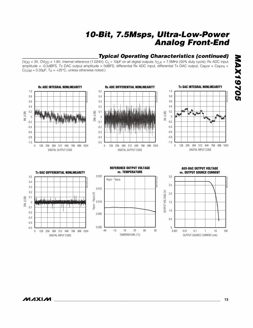
REFERENCE OUTPUT VOLTAGEvs. TEMPERATURE
MAX
1970
5 to
c32
TEMPERATURE (°C)
V REF
P - V
REFN
(V)
603510-15
0.505
0.510
0.515
0.520
0.500-40 85
VREFP - VREFN
AUX-DAC OUTPUT VOLTAGEvs. OUTPUT SOURCE CURRENT
MAX
1970
5 to
c33
OUTPUT SOURCE CURRENT (mA)
OUTP
UT V
OLTA
GE (V
)
1010.10.01
0.5
1.0
1.5
2.0
2.5
3.0
00.001 100
Rx ADC INTEGRAL NONLINEARITYM
AX19
705
toc2
8
DIGITAL OUTPUT CODE
INL
(LSB
)
896768512 640256 384128
-0.8
-0.6
-0.4
-0.2
0
0.2
0.4
0.6
0.8
1.0
-1.00 1024
Rx ADC DIFFERENTIAL NONLINEARITY
MAX
1970
5 to
c29
DIGITAL OUTPUT CODE
DNL
(LSB
)
896768512 640256 384128
-0.4
-0.3
-0.2
-0.1
0
0.1
0.2
0.3
0.4
0.5
-0.50 1024
Tx DAC INTEGRAL NONLINEARITY
MAX
1970
5 to
c30
DIGITAL INPUT CODE
INL
(LSB
)
896768512 640256 384128
-0.8
-0.6
-0.4
-0.2
0
0.2
0.4
0.6
0.8
1.0
-1.00 1024
Typical Operating Characteristics (continued)(VDD = 3V, OVDD = 1.8V, internal reference (1.024V), CL ≈ 10pF on all digital outputs, fCLK = 7.5MHz (50% duty cycle), Rx ADC inputamplitude = -0.5dBFS, Tx DAC output amplitude = 0dBFS, differential Rx ADC input, differential Tx DAC output, CREFP = CREFN =CCOM = 0.33µF, TA = +25°C, unless otherwise noted.)
AUX-DAC DIFFERENTIAL NONLINEARITY
MAX
1970
5 to
c37
DIGITAL INPUT CODE
DNL
(LSB
)
307220481024
-0.6
-0.4
-0.2
0
0.2
0.4
0.6
0.8
-0.80 4096
AUX-ADC INTEGRAL NONLINEARITY
MAX
1970
5 to
c38
DIGITAL OUTPUT CODE
INL
(LSB
)
896768512 640256 384128
1.5
1.0
0.5
0
-0.5
-1.0
-1.5
2.0
-2.00 1024
AUX-ADC DIFFERENTIAL NONLINEARITY
MAX
1970
5 to
c39
DIGITAL OUTPUT CODE
DNL
(LSB
)
896768640512384256128
-0.4
0
0.4
0.8
-0.80 1024
MA
X1
97
05
10-Bit, 7.5Msps, Ultra-Low-PowerAnalog Front-End
14 ______________________________________________________________________________________
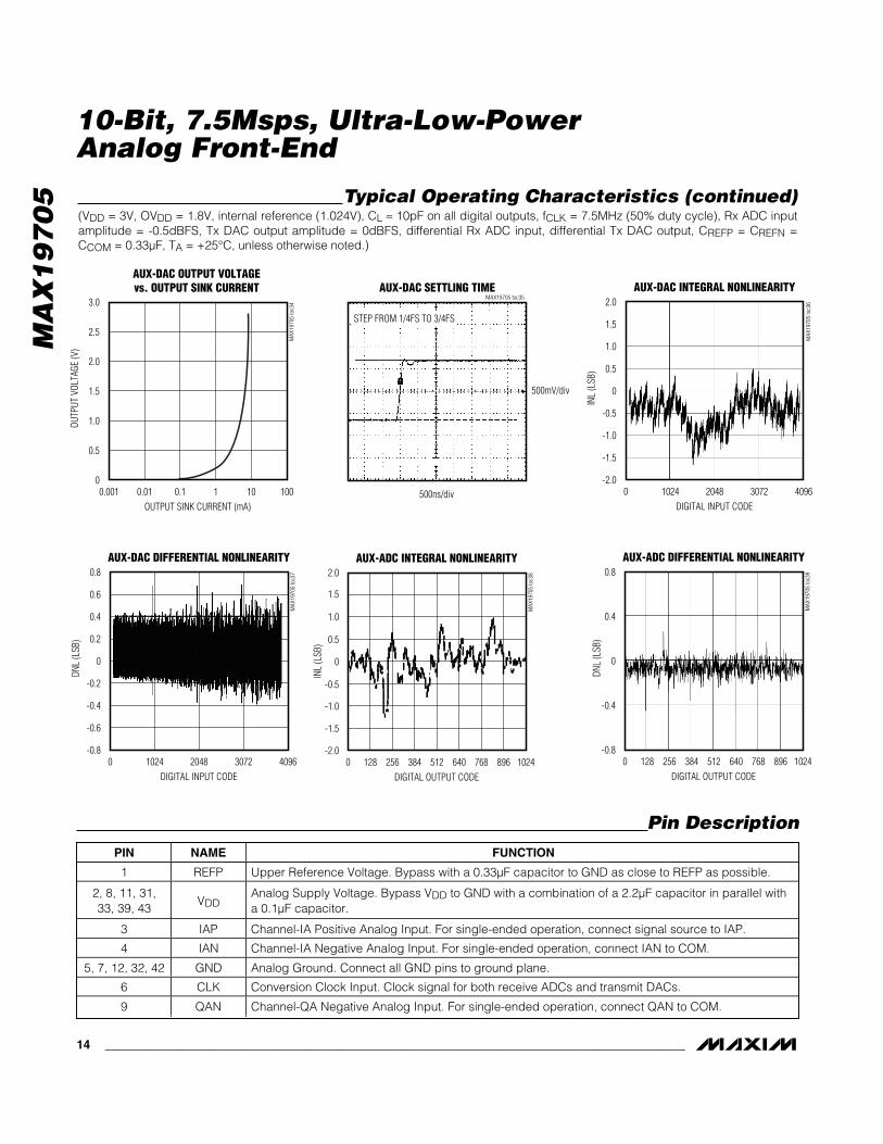
PIN NAME FUNCTION
1 REFP Upper Reference Voltage. Bypass with a 0.33µF capacitor to GND as close to REFP as possible.
2, 8, 11, 31,33, 39, 43
VDDAnalog Supply Voltage. Bypass VDD to GND with a combination of a 2.2µF capacitor in parallel witha 0.1µF capacitor.
3 IAP Channel-IA Positive Analog Input. For single-ended operation, connect signal source to IAP.
4 IAN Channel-IA Negative Analog Input. For single-ended operation, connect IAN to COM.
5, 7, 12, 32, 42 GND Analog Ground. Connect all GND pins to ground plane.
6 CLK Conversion Clock Input. Clock signal for both receive ADCs and transmit DACs.
9 QAN Channel-QA Negative Analog Input. For single-ended operation, connect QAN to COM.
Pin Description
AUX-DAC OUTPUT VOLTAGEvs. OUTPUT SINK CURRENT
MAX
1970
5 to
c34
OUTPUT SINK CURRENT (mA)
OUTP
UT V
OLTA
GE (V
)
1010.10.01
0.5
1.0
1.5
2.0
2.5
3.0
00.001 100
AUX-DAC SETTLING TIMEMAX19705 toc35
500ns/div
500mV/div
STEP FROM 1/4FS TO 3/4FS
AUX-DAC INTEGRAL NONLINEARITY
MAX
1970
5 to
c36
DIGITAL INPUT CODE
INL
(LSB
)
307220481024
-1.5
-1.0
-0.5
0
0.5
1.0
1.5
2.0
-2.00 4096
Typical Operating Characteristics (continued)(VDD = 3V, OVDD = 1.8V, internal reference (1.024V), CL ≈ 10pF on all digital outputs, fCLK = 7.5MHz (50% duty cycle), Rx ADC inputamplitude = -0.5dBFS, Tx DAC output amplitude = 0dBFS, differential Rx ADC input, differential Tx DAC output, CREFP = CREFN =CCOM = 0.33µF, TA = +25°C, unless otherwise noted.)

MA
X1
97
05
10-Bit, 7.5Msps, Ultra-Low-PowerAnalog Front-End
______________________________________________________________________________________ 15
PIN NAME FUNCTION
10 QAP Channel-QA Positive Analog Input. For single-ended operation, connect signal source to QAP.
13–18, 21–24 D0–D9Digital I/O. Outputs for receive ADC in Rx mode. Inputs for transmit DAC in Tx mode. D9 is the mostsignificant bit (MSB) and D0 is the least significant bit (LSB).
19 OGND Output-Driver Ground
20 OVDDOutput-Driver Power Supply. Supply range from +1.8V to VDD. Bypass OVDD to OGND with acombination of a 2.2µF capacitor in parallel with a 0.1µF capacitor.
25 SHDN Active-Low Shutdown Input. Apply logic-low to place the MAX19705 in shutdown.
26 DOUT Aux-ADC Digital Output
27 T/RTransmit- or Receive-Mode Select Input. T/R logic-low input sets the device in receive mode. Alogic-high input sets the device in transmit mode.
28 DIN 3-Wire Serial-Interface Data Input. Data is latched on the rising edge of the SCLK.
29 SCLK 3-Wire Serial-Interface Clock Input
30 CS 3-Wire Serial-Interface Chip-Select Input. Logic-low enables the serial interface.
34 ADC2 Analog Input for Auxiliary ADC
35 ADC1 Analog Input for Auxiliary ADC
36 DAC3 Analog Output for Auxiliary DAC3
37 DAC2 Analog Output for Auxiliary DAC2
38 DAC1 Analog Output for Auxiliary DAC1 (AFC DAC, VOUT = 1.1V During Power-Up)
40, 41 IDN, IDP DAC Channel-ID Differential Voltage Output
44, 45 QDN, QDP DAC Channel-QD Differential Voltage Output
46 REFIN Reference Input. Connect to VDD for internal reference.
47 COM Common-Mode Voltage I/O. Bypass COM to GND with a 0.33µF capacitor.
48 REFNNegative Reference I/O. Rx ADC conversion range is ±(VREFP - VREFN). Bypass REFN to GND with a0.1µF capacitor.
— EP Exposed Paddle. Exposed paddle is internally connected to GND. Connect EP to the GND plane.
Pin Description (continued)
SPI is a trademark of Motorola, Inc.MICROWIRE is a trademark of National Semiconductor Corp.
Detailed DescriptionThe MAX19705 integrates a dual 10-bit Rx ADC and adual 10-bit Tx DAC while providing ultra-low power andhigh dynamic performance at 7.5Msps conversion rate.The Rx ADC analog input amplifiers are fully differentialand accept 1.024VP-P full-scale signals. The Tx DACanalog outputs are fully differential with ±400mV full-scale output, selectable common-mode DC level, andadjustable I/Q offset trim.
The MAX19705 integrates three 12-bit auxiliary DAC(aux-DAC) channels and a 10-bit, 333ksps auxiliaryADC (aux-ADC) with 4:1 input multiplexer. The aux-DACchannels feature 1µs settling time for fast AGC, VGA,
and AFC level setting. The aux-ADC features data aver-aging to reduce processor overhead and a selectableclock-divider to program the conversion rate.
The MAX19705 includes a 3-wire serial interface tocontrol operating modes and power management. Theserial interface is SPI™ and MICROWIRE™ compatible.The MAX19705 serial interface selects shutdown, idle,standby, transmit (Tx), and receive (Rx) modes, as wellas controlling aux-DAC and aux-ADC channels.
The Rx ADC and Tx DAC share a common digital I/O toreduce the digital interface to a single 10-bit parallelmultiplexed bus. The 10-bit digital bus operates on asingle +1.8V to +3.3V supply.

MA
X1
97
05
10-Bit, 7.5Msps, Ultra-Low-PowerAnalog Front-End
16 ______________________________________________________________________________________
Figure 1. Rx ADC Internal T/H Circuits
S3b
S3a
COM
S5b
S5a
QAP
QAN
S1
OUT
OUT
C2a
C2b
S4c
S4a
S4b C1b
C1a
INTERNALBIAS
INTERNALBIAS
COM
HOLD HOLDCLK
INTERNALNONOVERLAPPINGCLOCK SIGNALS
TRACK TRACK
S2a
S2b
S3b
S3a
COM
S5b
S5a
IAP
IAN
S1
OUT
OUT
C2a
C2b
S4c
S4a
S4bC1b
C1a
INTERNALBIAS
INTERNALBIAS
COM
S2a
S2b
MAX19705
Dual 10-Bit Rx ADCThe ADC uses a seven-stage, fully differential, pipelinedarchitecture that allows for high-speed conversion whileminimizing power consumption. Samples taken at theinputs move progressively through the pipeline stagesevery half clock cycle. Including the delay through theoutput latch, the total clock-cycle latency is 5 clockcycles for channel IA and 5.5 clock cycles for channelQA. The ADC full-scale analog input range is ±VREFwith a VDD / 2 (±0.2V) common-mode input range. VREF
is the difference between VREFP and VREFN. See theReference Configurations section for details.
Input Track-and-Hold (T/H) CircuitsFigure 1 displays a simplified diagram of the Rx ADCinput track-and-hold (T/H) circuitry. Both ADC inputs(IAP, QAP, IAN, and QAN) can be driven either differen-tially or single-ended. Match the impedance of IAP andIAN, as well as QAP and QAN, and set the input signalcommon-mode voltage within the VDD / 2 (±200mV) Rx ADC range for optimum performance.

MA
X1
97
05
10-Bit, 7.5Msps, Ultra-Low-PowerAnalog Front-End
______________________________________________________________________________________ 17
Rx ADC System Timing RequirementsFigure 3 shows the relationship between the clock, ana-log inputs, and the resulting output data. Channel I(CHI) and channel Q (CHQ) are sampled on the risingedge of the clock signal (CLK) and the resulting data is
multiplexed at the D0–D9 outputs. CHI data is updatedon the rising edge and CHQ data is updated on thefalling edge of the CLK. Including the delay through theoutput latch, the total clock-cycle latency is 5 clockcycles for CHI and 5.5 clock cycles for CHQ.
Digital Input/Output Data (D0–D9)D0–D9 are the Rx ADC digital logic outputs when theMAX19705 is in receive mode. This bus is shared withthe Tx DAC digital logic inputs and operates in half-duplex mode. D0–D9 are the Tx DAC digital logic inputswhen the MAX19705 is in transmit mode. The logic levelis set by OVDD from 1.8V to VDD. The digital output cod-ing is offset binary (Table 1). Keep the capacitive loadon the digital outputs D0–D9 as low as possible (< 15pF)to avoid large digital currents feeding back into the ana-log portion of the MAX19705 and degrading its dynamicperformance. Buffers on the digital outputs isolate theoutputs from heavy capacitive loads. Adding 100Ω resis-tors in series with the digital outputs close to theMAX19705 will help improve Rx ADC and Tx DAC per-formance. Refer to the MAX19705EVKIT schematic foran example of the digital outputs driving a digital bufferthrough 100Ω series resistors.
During SHDN, IDLE, and STBY states, D0–D9 are inter-nally pulled up to prevent floating digital inputs. Toensure no current flows through D0–D9 I/O, the externalbus needs to be either tri-stated or pulled up to OVDDand should not be pulled to ground.
Table 1. Rx ADC Output Codes vs. Input Voltage
DIFFERENTIAL INPUTVOLTAGE DIFFERENTIAL INPUT (LSB) OFFSET BINARY (D0–D9) OUTPUT DECIMAL CODE
VREF x 512/512 511 (+Full Scale - 1 LSB) 11 1111 1111 1023
VREF x 511/512 510 (+Full Scale - 2 LSB) 11 1111 1110 1022
VREF x 1/512 +1 10 0000 0001 513
VREF x 0/512 0 (Bipolar Zero) 10 0000 0000 512
-VREF x 1/512 -1 01 1111 1111 511
-VREF x 511/512 -511 (-Full Scale +1 LSB) 00 0000 0001 1
-VREF x 512/512 -512 (-Full Scale) 00 0000 0000 0
Figure 2. Rx ADC Transfer Function
INPUT VOLTAGE (LSB)
-1-510 -509
10242 x VREF1 LSB = VREF = VREFP - VREFN
VREF VREF
V REF
V REF
0+ 1-511 +510 +512+511-512 +509
(COM)
(COM)
OFFS
ET B
INAR
Y OU
TPUT
COD
E (L
SB)
00 0000 000000 0000 000100 0000 001000 0000 0011
11 1111 111111 1111 111011 1111 1101
01 1111 111110 0000 000010 0000 0001

MA
X1
97
05
10-Bit, 7.5Msps, Ultra-Low-PowerAnalog Front-End
18 ______________________________________________________________________________________
Figure 3. Rx ADC System Timing Diagram
tDOQ
tCL tCH
tCLK
tDOI
5 CLOCK-CYCLE LATENCY (CHI)
5.5 CLOCK-CYCLE LATENCY (CHQ)
D0–D9 D0Q D1I D1Q D2I D2Q D3I D3Q D4I D4Q D5I D5Q D6I D6Q
CHI
CHQ
CLK
Table 2. Tx DAC Output Voltage vs. Input Codes (Internal Reference Mode VREFDAC = 1.024V, External Reference Mode VREFDAC = VREFIN; VFS = 400 for 800mVP-PFull Scale)
DIFFERENTIAL OUTPUT VOLTAGE (V) OFFSET BINARY (D0–D9) INPUT DECIMAL CODE
11 1111 1111 1023
11 1111 1110 1022
10 0000 0001 513
10 0000 0000 512
01 1111 1111 511
00 0000 0001 1
00 0000 0000 0
VV
FSREFDAC1024
10231023
( ) ×
VV
FSREFDAC1024
10211023
( ) ×
VV
FSREFDAC1024
31023
( ) ×
VV
FSREFDAC1024
11023
( ) ×
VV
FSREFDAC1024
11023
( ) ×−
VV
FSREFDAC1024
10211023
( ) ×−
VV
FSREFDAC1024
10231023
( ) ×−
Dual 10-Bit Tx DACThe dual 10-bit digital-to-analog converters (Tx DAC)operate with clock speeds up to 7.5MHz. The Tx DACdigital inputs, D0–D9, are multiplexed on a single 10-bitbus. The voltage reference determines the Tx DAC full-scale output voltage. See the Reference Configurationssection for details on setting the reference voltage.
The Tx DAC outputs at IDN, IDP and QDN, QDP arebiased at a 0.9V to 1.35V adjustable DC common-mode bias and designed to drive a differential inputstage with ≥ 70kΩ input impedance. This simplifies the
analog interface between RF quadrature upconvertersand the MAX19705. Many RF upconverters require a0.9V to 1.35V common-mode bias. The Tx DAC DCcommon-mode bias eliminates discrete level-settingresistors and code-generated level shifting while pre-serving the full dynamic range of each Tx DAC. The TxDAC differential analog outputs cannot be used in sin-gle-ended mode because of the internally generatedcommon-mode DC level. Table 2 shows the Tx DACoutput voltage vs. input codes. Table 10 shows theselection of DC common-mode levels. See Figure 4 foran illustration of the Tx DAC analog output levels.

MA
X1
97
05
10-Bit, 7.5Msps, Ultra-Low-PowerAnalog Front-End
______________________________________________________________________________________ 19
The Tx DACs also feature independent DC offset cor-rection of each I/Q channel. This feature is configuredthrough the SPI interface. The DC offset correction is
used to optimize sideband and carrier suppression inthe Tx signal path (see Table 9).
Figure 4. Tx DAC Common-Mode DC Level at IDN, IDP or QDN, QDP Differential Outputs
0
Tx DACI-CH
Tx DACQ-CH
FULL SCALE = 1.55V
VCOM = 1.35V
ZERO SCALE = 1.15V
0V
COMMON-MODE LEVEL
SELECT CM1 = 0, CM0 = 0VCOM = 1.35VVDIFF = ±400mV
EXAMPLE:
Tx RFIC INPUT REQUIREMENTS
• DC COMMON-MODE BIAS = 1.2V (MIN), 1.5V (MAX)
• BASEBAND INPUT = ±400mV DC-COUPLED
90
MAX19705
MA
X1
97
05
10-Bit, 7.5Msps, Ultra-Low-PowerAnalog Front-End
20 ______________________________________________________________________________________
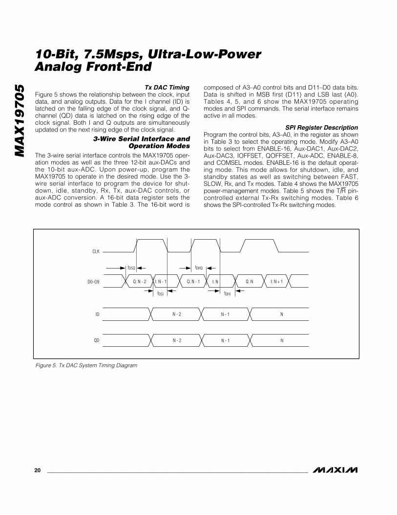
Figure 5. Tx DAC System Timing Diagram
tDSQ
tDSI
Q: N - 2 I: N - 1D0–D9
CLK
ID
QD
Q: N - 1 I: N Q: N I: N + 1
N - 2 N - 1 N
N - 2 N - 1 N
tDHQ
tDHI
Tx DAC TimingFigure 5 shows the relationship between the clock, inputdata, and analog outputs. Data for the I channel (ID) islatched on the falling edge of the clock signal, and Q-channel (QD) data is latched on the rising edge of theclock signal. Both I and Q outputs are simultaneouslyupdated on the next rising edge of the clock signal.
3-Wire Serial Interface andOperation Modes
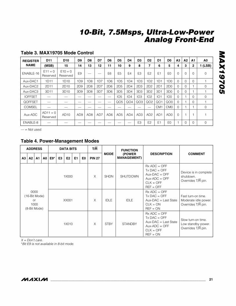
The 3-wire serial interface controls the MAX19705 oper-ation modes as well as the three 12-bit aux-DACs andthe 10-bit aux-ADC. Upon power-up, program theMAX19705 to operate in the desired mode. Use the 3-wire serial interface to program the device for shut-down, idle, standby, Rx, Tx, aux-DAC controls, oraux-ADC conversion. A 16-bit data register sets themode control as shown in Table 3. The 16-bit word is
composed of A3–A0 control bits and D11–D0 data bits.Data is shifted in MSB first (D11) and LSB last (A0).Tables 4, 5, and 6 show the MAX19705 operatingmodes and SPI commands. The serial interface remainsactive in all modes.
SPI Register DescriptionProgram the control bits, A3–A0, in the register as shownin Table 3 to select the operating mode. Modify A3–A0bits to select from ENABLE-16, Aux-DAC1, Aux-DAC2,Aux-DAC3, IOFFSET, QOFFSET, Aux-ADC, ENABLE-8,and COMSEL modes. ENABLE-16 is the default operat-ing mode. This mode allows for shutdown, idle, andstandby states as well as switching between FAST,SLOW, Rx, and Tx modes. Table 4 shows the MAX19705power-management modes. Table 5 shows the T/R pin-controlled external Tx-Rx switching modes. Table 6shows the SPI-controlled Tx-Rx switching modes.
MA
X1
97
05
10-Bit, 7.5Msps, Ultra-Low-PowerAnalog Front-End
______________________________________________________________________________________ 21
Table 4. Power-Management Modes
ADDRESS DATA BITS T/R
A3 A2 A1 A0 E9* E3 E2 E1 E0 PIN 27MODE
FUNCTION(POWER
MANAGEMENT)DESCRIPTION COMMENT
1X000 X SHDN SHUTDOWN
Rx ADC = OFFTx DAC = OFFAux-DAC = OFFAux-ADC = OFFCLK = OFFREF = OFF
Device is in completeshutdown.Overrides T/R pin.
XX001 X IDLE IDLE
Rx ADC = OFFTx DAC = OFFAux-DAC = Last StateCLK = ONREF = ON
Fast turn-on time.Moderate idle power.Overrides T/R pin.
0000(16-Bit Mode)
or1000
(8-Bit Mode)
1X010 X STBY STANDBY
Rx ADC = OFFTx DAC = OFFAux-DAC = Last StateAux-ADC = OFFCLK = OFFREF = ON
Slow turn-on time.Low standby power.Overrides T/R pin.
X = Don’t care.*Bit E9 is not available in 8-bit mode.
Table 3. MAX19705 Mode Control
D11 D10 D9 D8 D7 D6 D5 D4 D3 D2 D1 D0 A3 A2 A1 A0REGISTERNAME (MSB) 15 14 13 12 11 10 9 8 7 6 5 4 3 2 1 (LSB)
ENABLE-16E11 = 0
ReservedE10 = 0
ReservedE9 — — E6 E5 E4 E3 E2 E1 E0 0 0 0 0
Aux-DAC1 1D11 1D10 1D9 1D8 1D7 1D6 1D5 1D4 1D3 1D2 1D1 1D0 0 0 0 1
Aux-DAC2 2D11 2D10 2D9 2D8 2D7 2D6 2D5 2D4 2D3 2D2 2D1 2D0 0 0 1 0
Aux-DAC3 3D11 3D10 3D9 3D8 3D7 3D6 3D5 3D4 3D3 3D2 3D1 3D0 0 0 1 1
IOFFSET — — — — — — IO5 IO4 IO3 IO2 IO1 IO0 0 1 0 0
QOFFSET — — — — — — QO5 QO4 QO3 QO2 QO1 QO0 0 1 0 1
COMSEL — — — — — — — — — — CM1 CM0 0 1 1 0
Aux-ADCAD11 = 0Reserved
AD10 AD9 AD8 AD7 AD6 AD5 AD4 AD3 AD2 AD1 AD0 0 1 1 1
ENABLE-8 — — — — — — — — E3 E2 E1 E0 1 0 0 0
— = Not used.

MA
X1
97
05
10-Bit, 7.5Msps, Ultra-Low-PowerAnalog Front-End
22 ______________________________________________________________________________________
Table 5. External Tx-Rx Control Using T/R Pin (T/R = 0 = Rx Mode, T/R = 1 = Tx Mode)
ADDRESS DATA BITS T/R
A3 A2 A1 A0 E3 E2 E1 E0 PIN 27
STATEFUNCTION
Rx TO Tx-Tx TO RxSWITCHING SPEED
DESCRIPTION COMMENT
0 Ext1-Rx
Rx Mode:Rx ADC = ONTx DAC = ONRx Bus = Enable
Moderate Power:Fast Rx to Tx when T/Rtransitions 0 to 1.
0011
1 Ext1-Tx
FAST-SLOWTx Mode:Rx ADC = OFFTx DAC = ONTx Bus = Enable
Low Power:Slow Tx to Rx when T/Rtransitions 1 to 0.
0Ext2-Rx(Default)
Rx Mode:Rx ADC = ONTx DAC = OFFRx Bus = Enable
Low Power:Slow Rx to Tx when T/Rtransitions 0 to 1.
0100
1 Ext2-Tx
SLOW-FASTTx Mode:Rx ADC = ONTx DAC = ONTx Bus = Enable
Moderate Power:Fast Tx to Rx when T/Rtransitions 1 to 0.
0 Ext3-Rx
Rx Mode:Rx ADC = ONTx DAC = OFFRx Bus = Enable
Low Power:Slow Rx to Tx when T/Rtransitions 0 to 1.
0101
1 Ext3-Tx
SLOW-SLOWTx Mode:Rx ADC = OFFTx DAC = ONTx Bus = Enable
Low Power:Slow Tx to Rx when T/Rtransitions 1 to 0.
0 Ext4-Rx
Rx Mode:Rx ADC = ONTx DAC = ONRx Bus = Enable
Moderate Power:Fast Rx to Tx when T/Rtransitions 0 to 1.
0000(16-Bit Mode)
or1000
(8-Bit Mode)
0110
1 Ext4-Tx
FAST-FASTTx Mode:Rx ADC = ONTx DAC = ONTx Bus = Enable
Moderate Power:Fast Tx to Rx when T/Rtransitions 1 to 0.

MA
X1
97
05
10-Bit, 7.5Msps, Ultra-Low-PowerAnalog Front-End
______________________________________________________________________________________ 23
In ENABLE-16 mode, the aux-DACs have independentcontrol bits E4, E5, and E6, and bit E9 enables the aux-ADC. Table 7 shows the auxiliary DAC enable codesand Table 8 shows the auxiliary ADC enable code. BitsE11 and E10 are reserved. Program bits E11 and E10 tologic-low.
Modes aux-DAC1, aux-DAC2, and aux-DAC3 selectthe aux-DAC channels named DAC1, DAC2, andDAC3 and hold the data inputs for each DAC. Bits_D11–_D0 are the data inputs for each aux-DAC andcan be programmed through SPI. The MAX19705 alsoincludes two 6-bit registers that can be programmed toadjust the offsets for the Tx DAC I and Q channelsindependently (see Table 9). Use the COMSEL modeto select the output common-mode voltage with bitsCM1 and CM0 (see Table 10). Use aux-ADC mode tostart the auxiliary ADC conversion (see the 10-Bit,333ksps Auxiliary ADC section for details). UseENABLE-8 mode for faster enable and switchingbetween shutdown, idle, and standby states as well asswitching between FAST, SLOW, Rx and Tx modes.
Table 6. Tx-Rx Control Using SPI Commands
ADDRESS DATA BITS T/R
A3 A2 A1 A0 E3 E2 E1 E0 PIN 27
MODEFUNCTION
(Tx-Rx SWITCHINGSPEED)
DESCRIPTION COMMENTS
1011 X SPI1-Rx SLOW
Rx Mode:Rx ADC = ONTx DAC = OFFRx Bus = Enable
Low Power:Slow Rx to Tx throughSPI command.
1100 X SPI2-Tx SLOW
Tx Mode:Rx ADC = OFFTx DAC = ONTx Bus = Enable
Low Power:Slow Tx to Rx throughSPI command.
1101 X SPI3-Rx FAST
Rx Mode:Rx ADC = ONTx DAC = ONRx Bus = Enabled
Moderate Power:Fast Rx to Tx throughSPI command.
0000(16-Bit Mode)
or1000
(8-Bit Mode)
1110 X SPI4-Tx FAST
Tx Mode:Rx ADC = ONTx DAC = ONTx Bus = Enabled
Moderate Power:Fast Tx to Rx throughSPI command.
Table 7. Aux-DAC Enable Table(ENABLE-16 Mode)
E6 E5 E4 Aux-DAC3 Aux-DAC2 Aux-DAC1
0 0 0 ON ON ON
0 0 1 ON ON OFF
0 1 0 ON OFF ON
0 1 1 ON OFF OFF
1 0 0 OFF ON ON
1 0 1 OFF ON OFF
1 1 0 OFF OFF ON
1 1 1 OFF OFF OFF
Table 8. Aux-ADC Enable Table(ENABLE-16 Mode)
E9 SELECTION
0 (Default) Aux-ADC is Powered ON
1 Aux-ADC is Powered OFF
X = Don’t care.
MA
X1
97
05
10-Bit, 7.5Msps, Ultra-Low-PowerAnalog Front-End
24 ______________________________________________________________________________________
Shutdown mode offers the most dramatic power sav-ings by shutting down all the analog sections of theMAX19705 and placing the Rx ADC digital outputs intri-state mode. When the Rx ADC outputs transitionfrom tri-state to ON, the last converted word is placedon the digital outputs. The Tx DAC previously storeddata is lost when coming out of shutdown mode. Thewake-up time from shutdown mode is dominated by thetime required to charge the capacitors at REFP, REFN,and COM. In internal reference mode and bufferedexternal reference mode, the wake-up time is typically84.9µs to enter Rx mode and 26.4µs to enter Tx mode.
In idle mode, the reference and clock distribution cir-cuits are powered, but all other functions are off. The
Rx ADC outputs are forced to tri-state. The wake-uptime is 10.9µs to enter Rx mode and 6µs to enter Txmode. When the Rx ADC outputs transition from tri-state to ON, the last converted word is placed on thedigital outputs.
In standby mode, the reference is powered, but the restof the device functions are off. The wake-up time fromstandby mode is 17.6µs to enter Rx mode and 25µs toenter Tx mode. When the Rx ADC outputs transition fromtri-state to active, the last converted word is placed onthe digital outputs.
FAST and SLOW Rx and Tx ModesIn addition to the external Tx-Rx control, the MAX19705also features SLOW and FAST modes for switchingbetween Rx and Tx operation. In FAST Tx mode, the RxADC core is powered on but the ADC core digital out-puts are tri-stated on the D0–D9 bus; likewise, in FASTRx mode, the transmit DAC core is powered on but theDAC core digital inputs are tri-stated on the D0–D9 bus.The switching time between Tx to Rx or Rx to Tx is FASTbecause the converters are on and do not have torecover from a power-down state. In FAST mode, theswitching time between Rx to Tx and Tx to Rx is 0.5µs.
Table 9. Offset Control Bits for I and Q Channels (IOFFSET or QOFFSET Mode)BITS IO5–IO0 WHEN IN IOFFSET MODE, BITS QO5–QO0 WHEN IN QOFFSET MODE
IO5/QO5 IO4/QO4 IO3/QO3 IO2/QO2 IO1/QO1 IO0/QO0OFFSET 1 LSB =(VFSP-P / 1023)
1 1 1 1 1 1 -31 LSB
1 1 1 1 1 0 -30 LSB
1 1 1 1 0 1 -29 LSB
•
•
•
•
•
•
•
•
•
•
•
•
•
•
•
•
•
•
•
•
•
1 0 0 0 1 0 -2 LSB
1 0 0 0 0 1 -1 LSB
1 0 0 0 0 0 0mV
0 0 0 0 0 0 0mV (Default)
0 0 0 0 0 1 1 LSB
0 0 0 0 1 0 2 LSB
•
•
•
•
•
•
•
•
•
•
•
•
•
•
•
•
•
•
•
•
•
0 1 1 1 0 1 29 LSB
0 1 1 1 1 0 30 LSB
0 1 1 1 1 1 31 LSB
Note: For transmit full scale of ±400mV: 1 LSB = (800mVP-P / 1023) = 0.7820mV.
Table 10. Common-Mode Select (COMSEL Mode)
CM1 CM0 Tx DAC OUTPUT COMMON MODE (V)
0 0 1.35 (Default)
0 1 1.20
1 0 1.05
1 1 0.90

MA
X1
97
05
10-Bit, 7.5Msps, Ultra-Low-PowerAnalog Front-End
______________________________________________________________________________________ 25
However, power consumption is higher in this modebecause both the Tx and Rx cores are always on. Toprevent bus contention in these states, the Rx ADC out-put buffers are tri-stated during Tx and the Tx DACinput bus is tri-stated during Rx.
In SLOW mode, the Rx ADC core is off during Tx; likewisethe Tx DAC is turned off during Rx to yield lower powerconsumption in these modes. For example, the power inSLOW Tx mode is 22.2mW. The power consumption dur-ing Rx is 21mW compared to 28.2mW power consump-tion in FAST mode. However, the recovery time betweenstates is increased. The switching time in SLOW modebetween Rx to Tx is 6µs and Tx to Rx is 8.1µs.
External T/RR Switching Control vs.Serial-Interface Control
Bit E3 in the ENABLE-16 or ENABLE-8 register deter-mines whether the device Tx-Rx mode is controlledexternally through the T/R input (E3 = low) or through theSPI command (E3 = high). By default, the MAX19705 isin the external Tx-Rx control mode. In the external controlmode, use the T/R input (pin 27) to switch between Rx
and Tx modes. Using the T/R pin provides faster switch-ing between Rx and Tx modes. To override the externalTx-Rx control, program the MAX19705 through the serialinterface. During SHDN, IDLE, or STBY modes, the T/Rinput is overridden. To restore external Tx-Rx control,program bit E3 low and exit the SHDN, IDLE, or STBYmodes through the serial interface.
SPI TimingThe serial digital interface is a standard 3-wire connec-tion compatible with SPI/QSPI™/MICROWIRE/DSP inter-faces. Set CS low to enable the serial data loading atDIN or output at DOUT. Following a CS high-to-low tran-sition, data is shifted synchronously, most significant bitfirst, on the rising edge of the serial clock (SCLK). After16 bits are loaded into the serial input register, data istransferred to the latch when CS transitions high. CSmust transition high for a minimum of 80ns before thenext write sequence. The SCLK can idle either high orlow between transitions. Figure 6 shows the detailedtiming diagram of the 3-wire serial interface.
QSPI is a trademark of Motorola, Inc.
Figure 6. Serial-Interface Timing Diagram
16-BIT OR 8-BIT WRITE INTO SPI (DIN) 16-BIT OR 8-BIT WRITE INTO SPI DURING
AUX-ADC CONVERSION
10-BIT READ OUT OF AUX-ADC (DOUT) WITHSIMULTANEOUS 16-BIT WRITE INTO SPI (DIN)
tCHZ
LSBBIT A0(DIN)
BIT D1(DIN)LSBMSB
BIT D10(DIN)
LSBA0
DOUT = TRI-STATED WHENAUX-ADC IS IDLE
DOUT = ACTIVE WHENBIT AD0 IS SET
AUX-ADCIS BUSY
AUX-ADCDATA READY
MSBBIT D9(DOUT)
LSBBIT D0(DOUT)
LSBBIT D0(HELD)
DOUTTRI-
STATEDBIT AD0
CLEARED
D10 (16-BIT)D2 (8-BIT)
MSBD11 (16-BIT)D3 (8-BIT)
MSBBIT D11
(DIN)
tDCS
tCONV
tCSD
tCStCPtCSS
tCSW
tDS
tCH
tCL
tDH
tCD
SCLK
CS
DIN
DOUT

MA
X1
97
05
10-Bit, 7.5Msps, Ultra-Low-PowerAnalog Front-End
26 ______________________________________________________________________________________
Mode-Recovery TimingFigure 7 shows the mode-recovery timing diagram.tWAKE is the wakeup time when exiting shutdown, idle,or standby mode and entering Rx or Tx mode. tENABLEis the recovery time when switching between either Rxor Tx mode. tWAKE or tENABLE is the time for the Rx ADCto settle within 1dB of specified SINAD performance andTx DAC settling to 10 LSB error. tWAKE and tENABLEtimes are measured after either the 16-bit serial com-mand is latched into the MAX19705 by a CS transitionhigh (SPI controlled) or a T/R logic transition (externalTx-Rx control). In FAST mode, the recovery time is 0.5µsto switch between Tx or Rx modes.
System Clock Input (CLK)Both the Rx ADC and Tx DAC share the CLK input. TheCLK input accepts a CMOS-compatible signal level setby OVDD from 1.8V to VDD. Since the interstage con-version of the device depends on the repeatability of
the rising and falling edges of the external clock, use aclock with low jitter and fast rise and fall times (< 2ns).Specifically, sampling occurs on the rising edge of theclock signal, requiring this edge to provide the lowestpossible jitter. Any significant clock jitter limits the SNRperformance of the on-chip Rx ADC as follows:
where fIN represents the analog input frequency andtAJ is the time of the clock jitter.
Clock jitter is especially critical for undersamplingapplications. Consider the clock input as an analoginput and route away from any analog input or otherdigital signal lines. The MAX19705 clock input operateswith an OVDD / 2 voltage threshold and accepts a 50%±15% duty cycle.
logSNRf t
= ×× × ×
20
12 π IN AJ
Figure 7. Mode-Recovery Timing Diagram
SCLK
CS
DIN
D0-D9
ID/QD
T/RRx - > Tx
ADC DIGITAL OUTPUT.SINAD SETTLES WITHIN 1dB
DAC ANALOG OUTPUT.OUTPUT SETTLES TO 10 LSB ERROR
16-BIT SERIAL DATA INPUT
tENABLE, RX EXTERNAL T/R CONTROL
tENABLE, TX EXTERNAL T/R CONTROL
tWAKE, SD, ST_ TO Tx MODE OR tENABLE, TX
tWAKE, SD, ST_ TO Rx MODE OR tENABLE, RX
T/RTx - > Rx
MA
X1
97
05
10-Bit, 7.5Msps, Ultra-Low-PowerAnalog Front-End
______________________________________________________________________________________ 27
12-Bit, Auxiliary Control DACsThe MAX19705 includes three 12-bit aux-DACs (DAC1,DAC2, DAC3) with 1µs settling time for controlling vari-able-gain amplifier (VGA), automatic gain-control(AGC), and automatic frequency-control (AFC) func-tions. The aux-DAC output range is 0.1V to 2.56V.During power-up, the VGA and AGC outputs (DAC2and DAC3) are at zero. The AFC DAC (DAC1) is at 1.1Vduring power-up. The aux-DACs can be independentlycontrolled through the SPI bus, except during SHDNmode where the aux-DACs are turned off completelyand the output voltage is set to zero. In STBY and IDLEmodes the aux-DACs maintain the last value. On wakeupfrom SHDN, the aux-DACs resume the last values.
Loading on the aux-DAC outputs should be carefullyobserved to achieve specified settling time and stabili-ty. The capacitive load must be kept to a maximum of5pF including package and trace capacitance. Theresistive load must be greater than 200kΩ. If capacitiveloading exceeds 5pF, then add a 10kΩ resistor inseries with the output. Adding the series resistor helpsdrive larger load capacitance (< 15pF) at the expenseof slower settling time.
10-Bit, 333ksps Auxiliary ADCThe MAX19705 integrates a 333ksps, 10-bit aux-ADCwith an input 4:1 multiplexer. In the aux-ADC mode reg-ister, setting bit AD0 begins a conversion with the auxil-iary ADC. Bit AD0 automatically clears when theconversion is complete. Setting or clearing AD0 during
a conversion has no effect (see Table 11). Bit AD1determines the internal reference of the auxiliary ADC(see Table 12). Bits AD2 and AD3 determine the auxil-iary ADC input source (see Table 13). Bits AD4, AD5,and AD6 select the number of averages taken when asingle start-convert command is given. The conversiontime increases as the number of averages increases(see Table 14). The conversion clock can be divideddown from the system clock by properly setting bitsAD7, AD8, and AD9 (see Table 15). The aux-ADC out-put data can be written out of DOUT by setting bitAD10 high (see Table 16).
The aux-ADC features a 4:1 input multiplexer to allowmeasurements on four input sources. The input sourcesare selected by AD3 and AD2 (see Table 13). Two ofthe multiplexer inputs (ADC1 and ADC2) can be con-nected to external sources such as an RF power detec-tor like the MAX2208 or temperature sensor like theMAX6613. The other two multiplexer inputs are internalconnections to VDD and OVDD that monitor the power-supply voltages. The internal VDD and OVDD connec-tions are made through integrated resistor-dividers thatyield VDD / 2 and OVDD / 2 measurement results. Theaux-ADC voltage reference can be selected betweenan internal 2.048V bandgap reference or VDD (seeTable 12). The VDD reference selection is provided toallow measurement of an external voltage source with afull-scale range extending beyond the 2.048V level. Theinput source voltage range cannot extend above VDD.
Table 11. Auxiliary ADC Convert
Table 12. Auxiliary ADC Reference
Table 13. Auxiliary ADC Input SourceAD0 SELECTION
0 Aux-ADC Idle (Default)
1 Aux-ADC Start-Convert
AD1 SELECTION
0 Internal 2.048V Reference (Default)
1 Internal VDD Reference
AD3 AD2 AUX-ADC INPUT SOURCE
0 0 ADC1 (Default)
0 1 ADC2
1 0 VDD / 2
1 1 OVDD / 2

MA
X1
97
05
10-Bit, 7.5Msps, Ultra-Low-PowerAnalog Front-End
28 ______________________________________________________________________________________
The conversion requires 12 clock edges (1 for inputsampling, 1 for each of the 10 bits, and 1 at the end forloading into the serial output register) to complete oneconversion cycle (when no averaging is being done).Each conversion of an average (when averaging is setgreater than 1) requires 12 clock edges. The conver-sion clock is generated from the system clock input(CLK). An SPI-programmable divider divides the sys-tem clock by the appropriate divisor (set with bits AD7,AD8, and AD9; see Table 15) and provides the conver-sion clock to the auxiliary ADC. The auxiliary ADC has amaximum conversion rate of 333ksps. The maximumconversion clock frequency is 4MHz (333ksps x 12clocks). Choose the proper divider value to keep theconversion clock frequency under 4MHz, based uponthe system CLK frequency supplied to the MAX19705(see Table 15). The total conversion time (tCONV) of theauxiliary ADC can be calculated as tCONV = (12 xNAVG x NDIV) / fCLK; where NAVG is the number ofaverages (see Table 14), NDIV is the CLK divisor (seeTable 15), and fCLK is the system CLK frequency.
DOUT is normally in a tri-state condition. Upon settingthe auxiliary ADC start conversion bit (bit AD0), DOUTbecomes active and goes high, indicating that the aux-ADC is busy. When the conversion cycle is complete(including averaging), the data is placed into an outputregister and DOUT goes low, indicating that the outputdata is ready to be driven onto DOUT. When bit AD10 isset (AD10 = 1), the aux-ADC enters a data output modewhere data is available on DOUT upon the next asser-tion low of CS. The auxiliary ADC data is shifted out ofDOUT (MSB first) with the data transitioning on thefalling edge of the serial clock (SCLK). DOUT enters atri-state condition when CS is deasserted high. When bitAD10 is cleared (AD10 = 0), the aux-ADC data is notavailable on DOUT (see Table 16).
DIN can be written independent of DOUT state. A 16-bit instruction at DIN updates the device configuration.To prevent modifying internal registers while readingdata from DOUT, hold DIN at a high state. This effec-tively writes all ones into address 1111. Since address1111 does not exist, no internal registers are affected.
Table 14. Auxiliary ADC Averaging
Table 15. Auxiliary ADC Clock (CLK)Divider
Table 16. Auxiliary ADC Data OutputMode
AD10 SELECTION
0 Aux-ADC Data is Not Available on DOUT (Default)
1Aux-ADC Enters Data Output Mode Where
Data is Available on DOUT
AD6 AD5 AD4 AUX-ADC AVERAGING
0 0 0 1 Conversion (No Averaging) (Default)
0 0 1 Average of 2 Conversions
0 1 0 Average of 4 Conversions
0 1 1 Average of 8 Conversions
1 0 0 Average of 16 Conversions
1 0 1 Average of 32 Conversions
1 1 X Average of 32 Conversions
AD9 AD8 AD7 AUX-ADC CONVERSION CLOCK
0 0 0 CLK Divided by 1 (Default)
0 0 1 CLK Divided by 2
0 1 0 CLK Divided by 4
0 1 1 CLK Divided by 8
1 0 0 CLK Divided by 16
1 0 1 CLK Divided by 32
1 1 0 CLK Divided by 64
1 1 1 CLK Divided by 128
X = Don’t care.

MA
X1
97
05
10-Bit, 7.5Msps, Ultra-Low-PowerAnalog Front-End
______________________________________________________________________________________ 29
Reference ConfigurationsThe MAX19705 features an internal precision 1.024Vbandgap reference that is stable over the entire power-supply and temperature ranges. The REFIN input pro-vides two modes of reference operation. The voltage atREFIN (VREFIN) sets the reference operation mode(Table 17).
In internal reference mode, connect REFIN to VDD.VREF is an internally generated 0.512V ±4%. COM,REFP, and REFN are low-impedance outputs withVCOM = VDD / 2, VREFP = VDD / 2 + VREF / 2, andVREFN = VDD / 2 - VREF / 2. Bypass REFP, REFN, andCOM each with a 0.33µF capacitor. Bypass REFIN toGND with a 0.1µF capacitor.
In buffered external reference mode, apply 1.024V±10% at REFIN. In this mode, COM, REFP, and REFNare low-impedance outputs with VCOM = VDD / 2,VREFP = VDD / 2 + VREFIN / 4, and VREFN = VDD / 2 -VREFIN / 4. Bypass REFP, REFN, and COM each with a0.33µF capacitor. Bypass REFIN to GND with a 0.1µF capacitor. In this mode, the Tx DAC full-scale output isproportional to the external reference. For example, ifthe VREFIN is increased by 10% (max), the Tx DAC full-scale output is also increased by 10% or ±440mV.
Applications InformationUsing Balun Transformer AC-Coupling
An RF transformer (Figure 8) provides an excellentsolution to convert a single-ended signal source to afully differential signal for optimum ADC performance.Connecting the center tap of the transformer to COMprovides a VDD / 2 DC level shift to the input. A 1:1transformer can be used, or a step-up transformer canbe selected to reduce the drive requirements. In gener-al, the MAX19705 provides better SFDR and THD withfully differential input signals than single-ended signals,
especially for high input frequencies. In differentialmode, even-order harmonics are lower as both inputs(IAP, IAN, QAP, QAN) are balanced, and each of theRx ADC inputs only requires half the signal swing com-pared to single-ended mode. Figure 9 shows an RFtransformer converting the MAX19705 Tx DAC differen-tial analog outputs to single-ended.
Table 17. Reference ModesVREFIN REFERENCE MODE
> 0.8V x VDDInternal Reference Mode. VREF is internally generated to be 0.512V. Bypass REFP, REFN, and COM eachwith a 0.33µF capacitor.
1.024V ±10%Buffered External Reference Mode. An external 1.024V ±10% reference voltage is applied to REFIN. VREF isinternally generated to be VREFIN / 2. Bypass REFP, REFN, and COM each with a 0.33µF capacitor. BypassREFIN to GND with a 0.1µF capacitor.
Figure 8. Balun Transformer-Coupled Single-Ended-to-Differential Input Drive for Rx ADC
COM
IAP
IAN
25Ω
0.1µF0.33µF
25Ω
0.1µF
VIN
MAX19705
22pF
22pF
QAP
QAN
25Ω
0.1µF0.33µF
25Ω
0.1µF
VIN
22pF
22pF

MA
X1
97
05
10-Bit, 7.5Msps, Ultra-Low-PowerAnalog Front-End
30 ______________________________________________________________________________________
Using Op-Amp CouplingDrive the MAX19705 Rx ADC with op amps when abalun transformer is not available. Figures 10 and 11show the Rx ADC being driven by op amps for AC-cou-pled single-ended and DC-coupled differential applica-tions. Amplifiers such as the MAX4454 and MAX4354provide high speed, high bandwidth, low noise, andlow distortion to maintain the input signal integrity. Theop-amp circuit shown in Figure 11 can also be used tointerface with the Tx DAC differential analog outputs toprovide gain or buffering. The Tx DAC differential ana-log outputs cannot be used in single-ended modebecause of the internally generated common-modelevel. Also, the Tx DAC analog outputs are designed todrive a differential input stage with input impedance ≥ 70kΩ. If single-ended outputs are desired, use anamplifier to provide differential-to-single-ended conver-sion and select an amplifier with proper input common-mode voltage range.
TDD ModeThe MAX19705 is optimized to operate in TDD applica-tions. When FAST mode is selected, the MAX19705 canswitch between Tx and Rx modes through the T/R pinin typically 0.5µs. The Rx ADC and Tx DAC operateindependently. The Rx ADC and Tx DAC digital bus areshared forming a single 10-bit parallel bus. Using the 3-wire serial interface or external T/R pin, select betweenRx mode to enable the Rx ADC or Tx mode to enablethe Tx DAC. When operating in Rx mode, the Tx DACbus is not enabled and in Tx mode the Rx ADC bus istri-stated, eliminating any unwanted spurious emissionsand preventing bus contention. In TDD mode, theMAX19705 uses 28.2mW power at fCLK = 7.5MHz.
TDD ApplicationFigure 12 illustrates a typical TDD application circuit.The MAX19705 interfaces directly with the radio front-ends to provide a complete “RF-to-Bits” solution forTDD applications. The MAX19705 provides several sys-tem benefits to digital baseband developers.
• Fast Time-to-Market
• High-Performance, Low-Power Analog Functions
• Low Risk, Proven Analog Front-End Solution
• No Mixed-Signal Test Times
• No NRE Charges
• No IP Royalty Charges
• Enables Digital Baseband to Scale with 65nm to90nm CMOS
Figure 9. Balun Transformer-Coupled Differential-to-Single-Ended Output Drive for Tx DAC
MAX19705
IDP
IDN
VOUT
QDP
QDN
VOUT
Figure 10. Single-Ended Drive for Rx ADC
MAX19705
0.1µF
1kΩ
1kΩ100Ω
100Ω
CIN22pF
CIN22pF
QAP
QAN
COM
IAP
IAN
0.1µFRISO50Ω
RISO50Ω
REFP
REFN
VIN
0.1µF
1kΩ
1kΩ100Ω
100Ω
CIN22pF
CIN22pF
0.1µFRISO50Ω
RISO50Ω
REFP
REFN
VIN

MA
X1
97
05
10-Bit, 7.5Msps, Ultra-Low-PowerAnalog Front-End
______________________________________________________________________________________ 31
Figure 12. Typical Application Circuit for TDD Radio
DAC1
Rx-IRx
ENCODE
MAX19705
TDD RADIO
ZIF TRANSCEIVER
AGC
TCXO
10-BIT DAC
10-BIT ADC
12-BIT DAC
TxSOURCE
HALF-DUPLEX
BUS
DIGITALBASEBAND
ASIC
T/R
D9D0
SYSTEMCONTROLCLK DISTSPI REG
REF1.024VBUFFER
Rx-Q
Tx-I
Tx-Q
DAC3
DAC2
4:1 MUX 10-BIT, 333ksps
VDD
BATTERY VOLTAGE MONITOR
TEMPERATURE MEASURE
0VDD
ADC
CLK
SCLK
DIN
CS
SHDN
DOUT
REFINREFPREFN
COM
Figure 11. Rx ADC DC-Coupled Differential Drive
MAX19705
IAP
COM
IAN
RISO22Ω
RISO22Ω
R11600Ω
R9600Ω
R3600Ω
R2600Ω
R1600Ω
R10600Ω
R8600Ω
R5600Ω
R4600Ω
R7600Ω
R6600Ω
CIN5pF
CIN5pF

MA
X1
97
05
10-Bit, 7.5Msps, Ultra-Low-PowerAnalog Front-End
32 ______________________________________________________________________________________
0
2
1
4
3
7
6
5
000 010001 011 100 101 110
AT STEP011 (0.5 LSB)
AT STEP001 (0.25 LSB)
111DIGITAL INPUT CODE
ANAL
OG O
UTPU
T VA
LUE
Figure 13a. Integral Nonlinearity
0
2
1
4
3
6
5
000 010001 011 100 101
DIFFERENTIAL LINEARITYERROR (-0.25 LSB)
DIFFERENTIALLINEARITY ERROR (+0.25 LSB)
1 LSB
1 LSB
DIGITAL INPUT CODE
ANAL
OG O
UTPU
T VA
LUE
Figure 13b. Differential Nonlinearity
Grounding, Bypassing, andBoard Layout
The MAX19705 requires high-speed board layout designtechniques. Refer to the MAX19705 EV kit data sheet fora board layout reference. Place all bypass capacitors asclose to the device as possible, preferably on the sameside of the board as the device, using surface-mountdevices for minimum inductance. Bypass VDD to GNDwith a 0.1µF ceramic capacitor in parallel with a 2.2µFcapacitor. Bypass OVDD to OGND with a 0.1µF ceramiccapacitor in parallel with a 2.2µF capacitor. BypassREFP, REFN, and COM each to GND with a 0.33µFceramic capacitor. Bypass REFIN to GND with a 0.1µFcapacitor.
Multilayer boards with separated ground and powerplanes yield the highest level of signal integrity. Use asplit ground plane arranged to match the physical loca-tion of the analog ground (GND) and the digital output-driver ground (OGND) on the device package.Connect the MAX19705 exposed backside paddle toGND plane. Join the two ground planes at a singlepoint so the noisy digital ground currents do not inter-fere with the analog ground plane. The ideal locationfor this connection can be determined experimentallyat a point along the gap between the two groundplanes. Make this connection with a low-value, surface-mount resistor (1Ω to 5Ω), a ferrite bead, or a directshort. Alternatively, all ground pins could share thesame ground plane, if the ground plane is sufficientlyisolated from any noisy digital system’s ground plane(e.g., downstream output buffer or DSP ground plane).
Route high-speed digital signal traces away from sensi-tive analog traces. Make sure to isolate the analog
input lines to each respective converter to minimizechannel-to-channel crosstalk. Keep all signal linesshort and free of 90° turns.
Dynamic Parameter DefinitionsADC and DAC Static Parameter Definitions
Integral Nonlinearity (INL)Integral nonlinearity is the deviation of the values on anactual transfer function from a straight line. This straightline can be either a best-straight-line fit or a line drawnbetween the end points of the transfer function, onceoffset and gain errors have been nullified. The static lin-earity parameters for the device are measured usingthe best-straight-line fit (DAC Figure 13a).
Differential Nonlinearity (DNL)Differential nonlinearity is the difference between anactual step width and the ideal value of 1 LSB. A DNLerror specification of less than 1 LSB guarantees nomissing codes (ADC) and a monotonic transfer function(ADC and DAC) (DAC Figure 13b).
ADC Offset ErrorIdeally, the midscale transition occurs at 0.5 LSB abovemidscale. The offset error is the amount of deviationbetween the measured transition point and the idealtransition point.
DAC Offset ErrorOffset error (Figure 13a) is the difference between theideal and actual offset point. The offset point is the out-put value when the digital input is midscale. This erroraffects all codes by the same amount and usually canbe compensated by trimming.
MA
X1
97
05
10-Bit, 7.5Msps, Ultra-Low-PowerAnalog Front-End
______________________________________________________________________________________ 33
ADC Gain ErrorIdeally, the ADC full-scale transition occurs at 1.5 LSBbelow full scale. The gain error is the amount of devia-tion between the measured transition point and theideal transition point with the offset error removed.
ADC Dynamic Parameter DefinitionsAperture Jitter
Figure 14 shows the aperture jitter (tAJ), which is thesample-to-sample variation in the aperture delay.
Aperture DelayAperture delay (tAD) is the time defined between therising edge of the sampling clock and the instant whenan actual sample is taken (Figure 14).
Signal-to-Noise Ratio (SNR)For a waveform perfectly reconstructed from digitalsamples, the theoretical maximum SNR is the ratio ofthe full-scale analog input (RMS value) to the RMSquantization error (residual error) and results directlyfrom the ADC’s resolution (N bits):
SNR(max) = 6.02dB x N + 1.76dB (in dB)
In reality, there are other noise sources besides quanti-zation noise: thermal noise, reference noise, clock jitter,etc. SNR is computed by taking the ratio of the RMSsignal to the RMS noise. RMS noise includes all spec-tral components to the Nyquist frequency excluding thefundamental, the first five harmonics, and the DC offset.
Signal-to-Noise and Distortion (SINAD)SINAD is computed by taking the ratio of the RMS sig-nal to the RMS noise. RMS noise includes all spectralcomponents to the Nyquist frequency excluding thefundamental and the DC offset.
Effective Number of Bits (ENOB)ENOB specifies the dynamic performance of an ADC at aspecific input frequency and sampling rate. An idealADC’s error consists of quantization noise only. ENOB fora full-scale sinusoidal input waveform is computed from:
ENOB = (SINAD - 1.76) / 6.02
Total Harmonic Distortion (THD)THD is typically the ratio of the RMS sum of the first fiveharmonics of the input signal to the fundamental itself.This is expressed as:
where V1 is the fundamental amplitude and V2–V6 arethe amplitudes of the 2nd- through 6th-order harmonics.
Third Harmonic Distortion (HD3)HD3 is defined as the ratio of the RMS value of the thirdharmonic component to the fundamental input signal.
Spurious-Free Dynamic Range (SFDR)SFDR is the ratio expressed in decibels of the RMSamplitude of the fundamental (maximum signal compo-nent) to the RMS value of the next-largest spuriouscomponent, excluding DC offset.
Intermodulation Distortion (IMD)IMD is the total power of the intermodulation productsrelative to the total input power when two tones, f1 andf2, are present at the inputs. The intermodulation prod-ucts are (f1 ± f2), (2 f1), (2 f2), (2 f1 ± f2), (2 f2 ± f1). The individual input tone levels are at -7dBFS.
3rd-Order Intermodulation (IM3)IM3 is the power of the worst 3rd-order intermodulationproduct relative to the input power of either input tonewhen two tones, f1 and f2, are present at the inputs. The3rd-order intermodulation products are (2 x f1 ± f2), (2
f2 ± f1). The individual input tone levels are at -7dBFS.
THD (V + V + V + V + V )
V22
32
42
52
62
1=
20 x log
HOLD
ANALOGINPUT
SAMPLEDDATA (T/H)
T/H
tADtAJ
TRACK TRACK
CLK
Figure 14. T/H Aperture Timing

MA
X1
97
05
10-Bit, 7.5Msps, Ultra-Low-PowerAnalog Front-End
34 ______________________________________________________________________________________
Power-Supply RejectionPower-supply rejection is defined as the shift in offsetand gain error when the power supply is changed ±5%.
Small-Signal BandwidthA small -20dBFS analog input signal is applied to anADC in such a way that the signal’s slew rate does notlimit the ADC’s performance. The input frequency isthen swept up to the point where the amplitude of thedigitized conversion result has decreased by 3dB. Notethat the T/H performance is usually the limiting factorfor the small-signal input bandwidth.
Full-Power BandwidthA large -0.5dBFS analog input signal is applied to anADC, and the input frequency is swept up to the pointwhere the amplitude of the digitized conversion resulthas decreased by 3dB. This point is defined as the full-power bandwidth frequency.
DAC Dynamic Parameter DefinitionsTotal Harmonic Distortion
THD is the ratio of the RMS sum of the output harmonicsup to the Nyquist frequency divided by the fundamental:
where V1 is the fundamental amplitude and V2 throughVn are the amplitudes of the 2nd through nth harmonicup to the Nyquist frequency.
Spurious-Free Dynamic RangeSpurious-free dynamic range (SFDR) is the ratio of RMSamplitude of the fundamental (maximum signal compo-nent) to the RMS value of the next-largest distortioncomponent up to the Nyquist frequency excluding DC.
THD (V + V + ... + V )
V22
32
n2
1=
20 x log
Selector Guide
PART DESCRIPTIONSAMPLING RATE
(Msps)
MAX19700Dual 10-Bit Rx ADC, Dual 10-Bit Tx DAC, Integrated TD-SCDMA
Filters, Three 12-Bit Auxiliary DACs7.5
MAX19708Dual 10-Bit Rx ADC, Dual 10-Bit Tx DAC, Integrated TD-SCDMAFilters, Three 12-Bit Auxiliary DACs, 10-Bit Auxiliary ADC with 4:1
Input Mux11
MAX19705/MAX19706†/MAX19707† Dual 10-Bit Rx ADC, Dual 10-Bit Tx DAC, Three 12-Bit AuxiliaryDACs, 10-Bit Auxiliary ADC with 4:1 Input Mux
7.5/22/45
†Future product—contact factory for availability.

MA
X1
97
05
10-Bit, 7.5Msps, Ultra-Low-PowerAnalog Front-End
______________________________________________________________________________________ 35
CLK
SERIALINTERFACE
AND SYSTEMCONTROL
IAP
IAN
QAP
QAN
IDP
IDN
QDP
QDN
REFPREFNCOM
DOUT
REFIN
DINSCLKCS
SYSTEMCLOCK
PROGRAMMABLEOFFSET/CM
1.024V REFERENCE
BUFFER
10-BITADC
10-BITADC
10-BITDAC
HALF-DUPLEX
BUS
10-BITDAC
12-BITDAC
12-BITDAC
12-BITDAC
4:1 MUX
GND
VDD 0VDD
DAC1
DAC2
DAC3
ADC1
D0–D9
SHDN
T/R
MAX19705
10-BITADCADC2
OGND
VDD = +2.7V TO +3.3V OVDD = +1.8V TO +3.3V
Functional Diagram

MA
X1
97
05
10-Bit, 7.5Msps, Ultra-Low-PowerAnalog Front-End
36 ______________________________________________________________________________________
32, 4
4, 4
8L Q
FN
.EP
S
e
L
e
L
A1A
A2
E/2
E
D/2
D
DETAIL A
D2/2
D2
b
L
k
E2/2
E2(NE-1) X e
(ND-1) X e
e
CLCL
CL
CL
k
DETAIL B
e
L
L1
PROPRIETARY INFORMATION
DOCUMENT CONTROL NO.APPROVAL
TITLE:
REV.
21
21-0144
DALLASSEMICONDUCTOR
PACKAGE OUTLINE32, 44, 48, 56L THIN QFN, 7x7x0.8mm
D
Package Information(The package drawing(s) in this data sheet may not reflect the most current specifications. For the latest package outline information,go to www.maxim-ic.com/packages.)
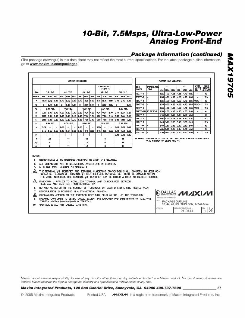
MA
X1
97
05
10-Bit, 7.5Msps, Ultra-Low-PowerAnalog Front-End
Maxim cannot assume responsibility for use of any circuitry other than circuitry entirely embodied in a Maxim product. No circuit patent licenses areimplied. Maxim reserves the right to change the circuitry and specifications without notice at any time.
Maxim Integrated Products, 120 San Gabriel Drive, Sunnyvale, CA 94086 408-737-7600 ____________________ 37
© 2005 Maxim Integrated Products Printed USA is a registered trademark of Maxim Integrated Products, Inc.
Quijano
PROPRIETARY INFORMATION
DOCUMENT CONTROL NO.APPROVAL
TITLE:
REV.
22
21-0144
DALLASSEMICONDUCTOR
PACKAGE OUTLINE32, 44, 48, 56L THIN QFN, 7x7x0.8mm
D
Package Information (continued)(The package drawing(s) in this data sheet may not reflect the most current specifications. For the latest package outline information,go to www.maxim-ic.com/packages.)