Evaluating spin-on carbon materials at low temperatures ... · Evaluating spin-on carbon materials...
9
Evaluating spin-on carbon materials at low temperatures for high wiggling resistance Michael Weigand, Vandana Krishnamurthy, Yubao Wang, Qin Lin, Douglas Guerrero, Sean Simmons, Brandy Carr Brewer Science, Inc., 2401 Brewer Drive, Rolla, MO, USA 65401 ABSTRACT Spin-on carbon (SOC) materials play an important role in the multilayer lithography scheme for the mass production of advanced semiconductor devices. One of the SOC’s key roles in the multilayer process (photoresist, silicon-containing hardmask, SOC) is the reactive ion etch (RIE) for pattern transfer into the substrate. As aspect ratios of the SOC material increase and feature sizes decrease, the pattern transfer from SOC to substrate by a fluorine-containing RIE induces severe pattern deformation (“wiggling”), which ultimately prevents successful pattern transfer into the substrate. One process that reduces line wiggling is a high-temperature (>250°C) post-application bake of the SOC material. In this study, we developed a process for evaluating SOC materials with respect to their pattern transfer performance. This process allowed us to evaluate line-wiggling behavior with several SOC materials at lower bake temperatures. This paper will discuss novel materials design in relation to high-aspect-ratio SOC layers and wiggling resistance. Keywords: spin-on carbon, carbon hardmask, lithography, silicon hardmask, wiggling, pattern transfer, reactive ion etching 1. INTRODUCTION Reactive ion etching (RIE) is an integral part of semiconductor integrated circuit (IC) processing and a key process in the multilayer lithography scheme. With the introduction of polymethacrylate photoresist polymers in 193-nm (ArF) lithography came a reduction in the thickness of the photoresist, limitations for depth of focus at high numerical aperture (NA), and other factors that made the photoresist no longer a capable of acting as a mask for transfer into the substrate. 1,2 Therefore, a new multilayer scheme consisting of photoresist, silicon-containing hardmask material (Si-HM), and spin-on carbon (SOC), also referred to as a carbon hardmask, has been developed and implemented to achieve smaller nodes. The goal of the multilayer scheme is to transfer the pattern or line from the photolithography process into the substrate. One of the key components to make the multilayer scheme work is the RIE process in which the plasma etch selectivity between the different layers (photoresist, Si-HM, and SOC) in fluorinated etch gases and oxygen-rich etch gases allows the pattern to be transferred. The last step in the RIE process is the pattern transfer from the SOC into the substrate. As aspect ratios of the SOC material increase and feature sizes decrease, the pattern transfer from SOC to substrate by fluorine-containing RIE induces severe pattern deformation (“wiggling”), which ultimately prevents successful pattern transfer into the substrate. 3 One process that reduces line wiggling is a high-temperature (>250°C) post-application bake (PAB)
Transcript of Evaluating spin-on carbon materials at low temperatures ... · Evaluating spin-on carbon materials...
Evaluating spin-on carbon materials at low temperatures for high wiggling resistance
Michael Weigand, Vandana Krishnamurthy, Yubao Wang, Qin Lin, Douglas Guerrero,
Sean Simmons, Brandy Carr Brewer Science, Inc., 2401 Brewer Drive, Rolla, MO, USA 65401
ABSTRACT
Spin-on carbon (SOC) materials play an important role in the multilayer lithography scheme for the mass production of advanced semiconductor devices. One of the SOC’s key roles in the multilayer process (photoresist, silicon-containing hardmask, SOC) is the reactive ion etch (RIE) for pattern transfer into the substrate. As aspect ratios of the SOC material increase and feature sizes decrease, the pattern transfer from SOC to substrate by a fluorine-containing RIE induces severe pattern deformation (“wiggling”), which ultimately prevents successful pattern transfer into the substrate. One process that reduces line wiggling is a high-temperature (>250°C) post-application bake of the SOC material. In this study, we developed a process for evaluating SOC materials with respect to their pattern transfer performance. This process allowed us to evaluate line-wiggling behavior with several SOC materials at lower bake temperatures. This paper will discuss novel materials design in relation to high-aspect-ratio SOC layers and wiggling resistance.
Keywords: spin-on carbon, carbon hardmask, lithography, silicon hardmask, wiggling, pattern transfer, reactive ion etching
1. INTRODUCTION
Reactive ion etching (RIE) is an integral part of semiconductor integrated circuit (IC) processing and a key process in the multilayer lithography scheme. With the introduction of polymethacrylate photoresist polymers in 193-nm (ArF) lithography came a reduction in the thickness of the photoresist, limitations for depth of focus at high numerical aperture (NA), and other factors that made the photoresist no longer a capable of acting as a mask for transfer into the substrate.1,2 Therefore, a new multilayer scheme consisting of photoresist, silicon-containing hardmask material (Si-HM), and spin-on carbon (SOC), also referred to as a carbon hardmask, has been developed and implemented to achieve smaller nodes. The goal of the multilayer scheme is to transfer the pattern or line from the photolithography process into the substrate. One of the key components to make the multilayer scheme work is the RIE process in which the plasma etch selectivity between the different layers (photoresist, Si-HM, and SOC) in fluorinated etch gases and oxygen-rich etch gases allows the pattern to be transferred. The last step in the RIE process is the pattern transfer from the SOC into the substrate. As aspect ratios of the SOC material increase and feature sizes decrease, the pattern transfer from SOC to substrate by fluorine-containing RIE induces severe pattern deformation (“wiggling”), which ultimately prevents successful pattern transfer into the substrate.3 One process that reduces line wiggling is a high-temperature (>250°C) post-application bake (PAB)
Catherine Frank
Text Box
M. Weigand, V. Krishnamurthy, Y. Wang, Q. Lin, D. Guerrero, S. Simmons, B. Carr, "Evaluating spin-on carbon materials at low temperatures for high wiggling resistance," Proceedings of SPIE, vol. 8685, 2013. © 2013 Society of Photo-Optical Instrumentation Engineers. One print or electronic copy may be made for personal use only. Systematic reproduction and distribution, duplication of any material in the paper for a fee or for commercial purposes, or modification of the content of the paper are prohibited.
of the SOC material.2 One popular model used to describe basic polymer RIE is the Ohnishi parameter, which states that the etch rate is proportional to the effective carbon content in the polymer according to the function NT/(NC-NO), where NT is the total number of atoms, NC is the number of carbon atoms, and NO is the number of oxygen atoms.4 However, this model does not take into account the hydrogen content of the material. In many publications, the hydrogen content was crucial to reduce line wiggling.2,3 In this paper, we will study materials where hydrogen was not the overall dominant factor to determine wiggle resistance. Instead the chemistry makeup as a whole as well as the overall density of the material are important. Another common problem in the multilayer scheme is the removal of the SOC material after pattern transfer into the substrate without damaging the substrate with further RIE. One solution to this problem is to use an SOC that can be removed with common developer and not another plasma etch. In this study, we developed a process for evaluating SOC materials with respect to their pattern transfer performance. This process allowed us to evaluate line-wiggling behavior with several SOC materials at lower bake temperatures. This paper will discuss novel materials design in relation to high-aspect-ratio SOC layers and wiggling resistance.
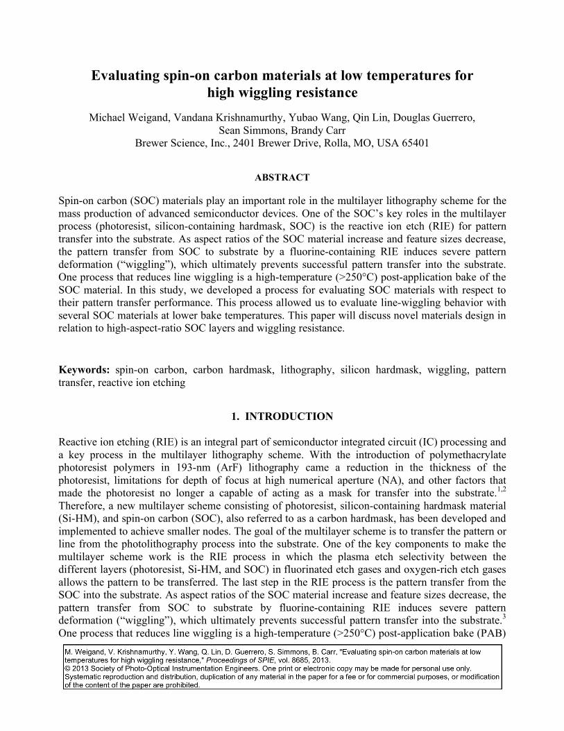
2. EXPERIMENTAL The polymers tested in this study were synthesized at Brewer Science, Inc. The SOC formulations were blends of polymers, crosslinkers, catalysts, and other additives. All materials are protected by patents or are covered in previous technical publications. SOC1 has a low PAB temperature of 225°C. SOC2 has a high hydrogen content and a high PAB temperature of 300°C. SOC3 has a high hydrogen content and a low PAB temperature of 205°C. These formulations were spin coated on silicon wafers and baked at the temperatures listed above to cure the films. The multilayer process to etch into the substrate is shown below in Figure 1.
Figure 1. Multilayer scheme process flow.

2.1 Lithography Conditions Each multilayer scheme consisted of one of the three different SOC materials (300 nm) to be tested for line wiggling, a Si-HM (OptiStack® HM9825-302.6 material [26 nm] commercially available from Brewer Science), and a common commercially available photoresist used in 193-nm lithography. All these materials were spin coated onto a silicon wafer and baked. After these materials were applied, they were exposed on an ASML 1250 ArF scanner. Lithography conditions are listed in Table 1.
Parameter Conditions Resist thickness: 165 nm Resist coat: 2100 rpm, 40 s Target: 65L/130P Post-application bake (PAB) 100°C, 60 s Illumination mode: Dipole 40Y NA: 0.85 Sigma (outer, inner): 0.92, 0.62 Center dose, step: 51 mJ/cm2, 1 mJ/cm2 Focus offset, step: 0 µm, 0.05 µm Post-exposure bake (PEB): 105°C, 60 s Developer type, time: OPD262, 60 s
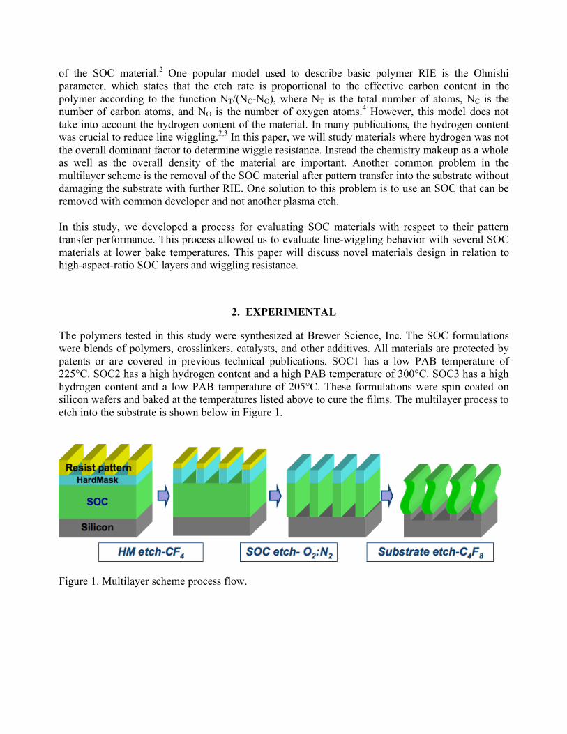
Table 1. Lithography conditions of ASML 1250 ArF scanner. First a focus-exposure matrix (FEM) wafer was created to find best focus and exposure. Once these conditions were established, a production-style wafer was produced. Each production-style wafer was a wafer with one die repeated consistently across the wafer shot at the same dose and focus. 2.2 Multilayer-Scheme Pattern Transfer All pattern transfer experiments were conducted with an Oxford Plasmalab® 80 Plus RIE system with no end point detection and no inductively coupled plasma (ICP). Step one is the pattern transfer from photoresist into the Si-HM. See Figure 2.
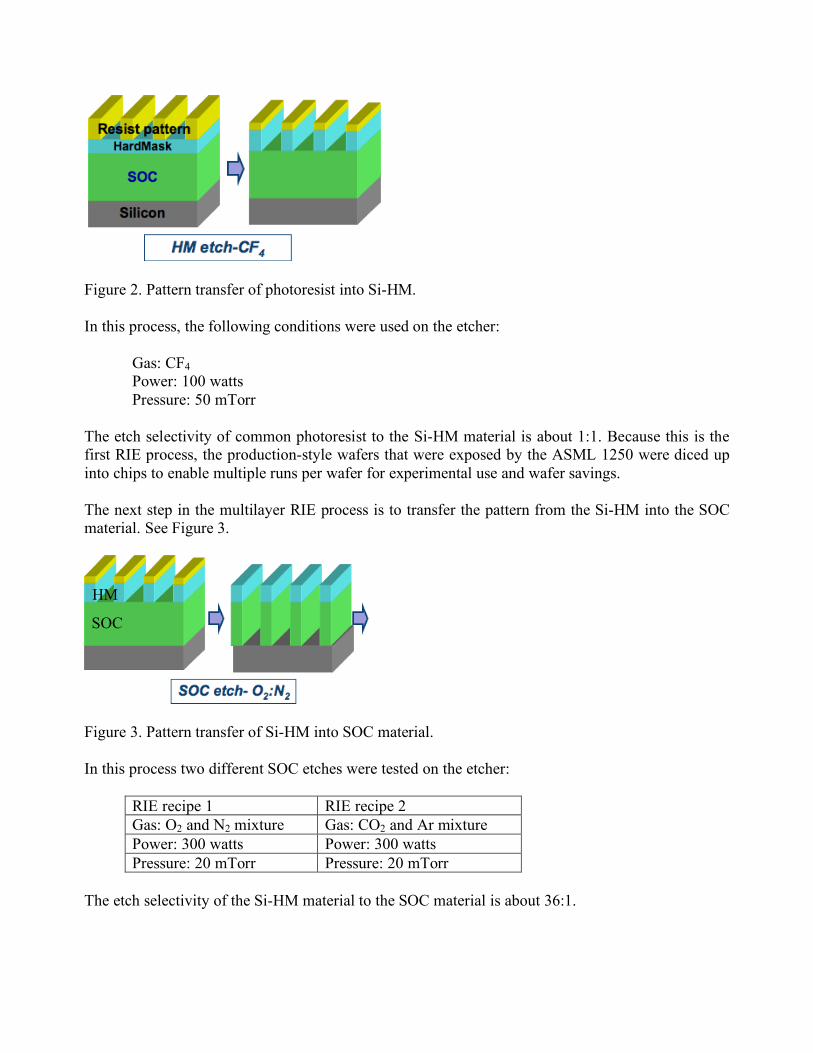
Figure 2. Pattern transfer of photoresist into Si-HM. In this process, the following conditions were used on the etcher:
Gas: CF4 Power: 100 watts Pressure: 50 mTorr
The etch selectivity of common photoresist to the Si-HM material is about 1:1. Because this is the first RIE process, the production-style wafers that were exposed by the ASML 1250 were diced up into chips to enable multiple runs per wafer for experimental use and wafer savings. The next step in the multilayer RIE process is to transfer the pattern from the Si-HM into the SOC material. See Figure 3.
Figure 3. Pattern transfer of Si-HM into SOC material. In this process two different SOC etches were tested on the etcher:
RIE recipe 1 RIE recipe 2 Gas: O2 and N2 mixture Gas: CO2 and Ar mixture Power: 300 watts Power: 300 watts Pressure: 20 mTorr Pressure: 20 mTorr
The etch selectivity of the Si-HM material to the SOC material is about 36:1.
SOC
HM
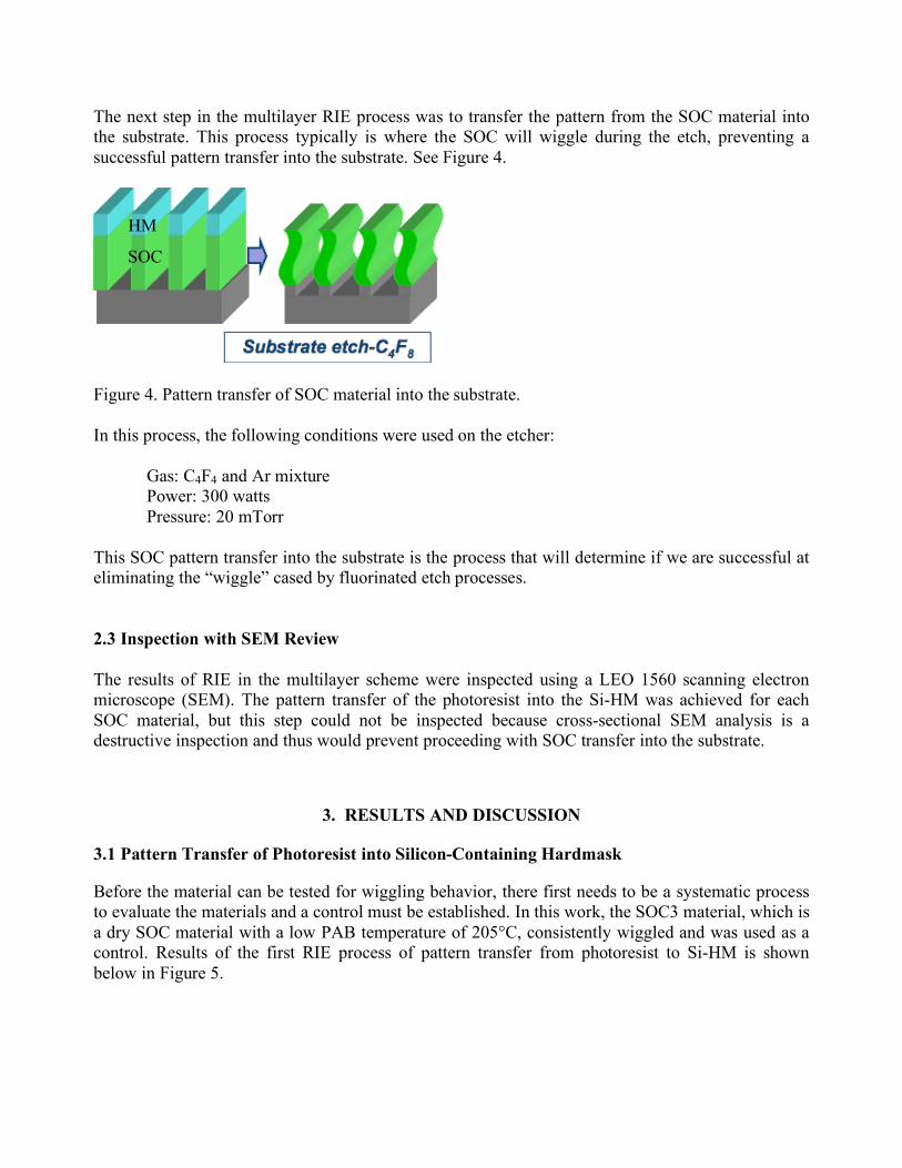
The next step in the multilayer RIE process was to transfer the pattern from the SOC material into the substrate. This process typically is where the SOC will wiggle during the etch, preventing a successful pattern transfer into the substrate. See Figure 4.
Figure 4. Pattern transfer of SOC material into the substrate. In this process, the following conditions were used on the etcher:
Gas: C4F4 and Ar mixture Power: 300 watts Pressure: 20 mTorr
This SOC pattern transfer into the substrate is the process that will determine if we are successful at eliminating the “wiggle” cased by fluorinated etch processes. 2.3 Inspection with SEM Review The results of RIE in the multilayer scheme were inspected using a LEO 1560 scanning electron microscope (SEM). The pattern transfer of the photoresist into the Si-HM was achieved for each SOC material, but this step could not be inspected because cross-sectional SEM analysis is a destructive inspection and thus would prevent proceeding with SOC transfer into the substrate.
3. RESULTS AND DISCUSSION 3.1 Pattern Transfer of Photoresist into Silicon-Containing Hardmask Before the material can be tested for wiggling behavior, there first needs to be a systematic process to evaluate the materials and a control must be established. In this work, the SOC3 material, which is a dry SOC material with a low PAB temperature of 205°C, consistently wiggled and was used as a control. Results of the first RIE process of pattern transfer from photoresist to Si-HM is shown below in Figure 5.
SOC
HM

Figure 5. SEM after pattern transfer from photoresist to Si-HM. This SEM picture demonstrates successful pattern transfer of the Si-HM material. A slight over-etch was used in subsequent etch runs because there was no end point detection on the etch tool, all etches were timed. Therefore, six different times were tested and repeated to ensure the proper hardmask etch time was established. Also some photoresist remained on top of the Si-HM, but that would all be removed once the SOC etch begins. The next step is the pattern transfer of the Si-HM into the SOC materials SOC1 and SOC3. See Figures 6 and 7.
Figure 6. SEM photo taken after pattern transfer from Si-HM into SOC1, O2:N2.
Figure 7. SEM photo taken after pattern transfer from Si-HM into SOC3, O2:N2.
The cross-sectional SEM images show the successful pattern transfer of the Si-HM into both SOC1 and SOC3. SOC2 was also successfully transferred but is not shown. Each SOC material maintained it full height of about 300 nm. It should be noted there is still hardmask on top of the SOC material if further SOC etch is needed. Similar to the hardmask etch, six different etch times were tested and repeated to find the correct etch time. For Figures 6 and 7, the O2:N2 RIE recipe was used. Figures 8 and 9 show results for the SOC etch where the RIE recipe used a CO2:Ar gas mixture.
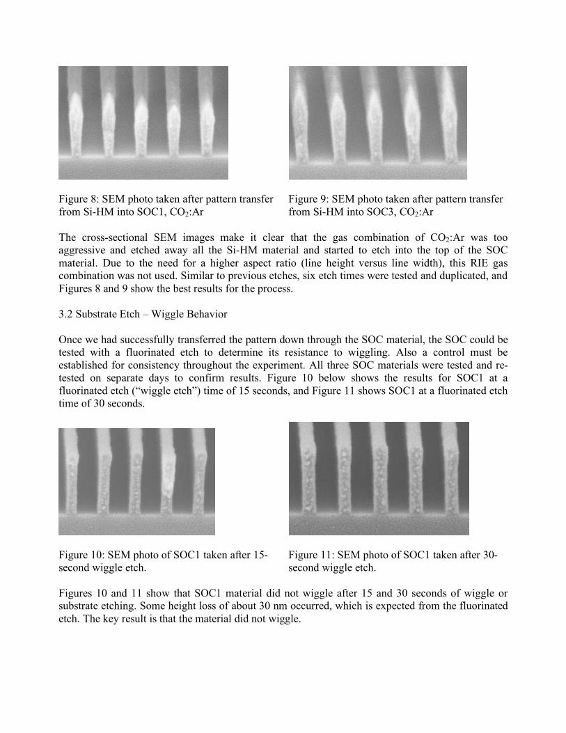
Figure 8: SEM photo taken after pattern transfer from Si-HM into SOC1, CO2:Ar
Figure 9: SEM photo taken after pattern transfer from Si-HM into SOC3, CO2:Ar
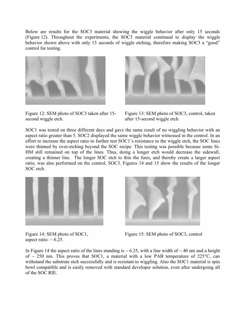
The cross-sectional SEM images make it clear that the gas combination of CO2:Ar was too aggressive and etched away all the Si-HM material and started to etch into the top of the SOC material. Due to the need for a higher aspect ratio (line height versus line width), this RIE gas combination was not used. Similar to previous etches, six etch times were tested and duplicated, and Figures 8 and 9 show the best results for the process. 3.2 Substrate Etch – Wiggle Behavior Once we had successfully transferred the pattern down through the SOC material, the SOC could be tested with a fluorinated etch to determine its resistance to wiggling. Also a control must be established for consistency throughout the experiment. All three SOC materials were tested and re-tested on separate days to confirm results. Figure 10 below shows the results for SOC1 at a fluorinated etch (“wiggle etch”) time of 15 seconds, and Figure 11 shows SOC1 at a fluorinated etch time of 30 seconds.
Figure 10: SEM photo of SOC1 taken after 15-second wiggle etch.
Figure 11: SEM photo of SOC1 taken after 30-second wiggle etch.
Figures 10 and 11 show that SOC1 material did not wiggle after 15 and 30 seconds of wiggle or substrate etching. Some height loss of about 30 nm occurred, which is expected from the fluorinated etch. The key result is that the material did not wiggle.
Below are results for the SOC3 material showing the wiggle behavior after only 15 seconds (Figure 12). Throughout the experiments, the SOC3 material continued to display the wiggle behavior shown above with only 15 seconds of wiggle etching, therefore making SOC3 a “good” control for testing.
Figure 12: SEM photo of SOC3 taken after 15-second wiggle etch.
Figure 13: SEM photo of SOC3, control, taken after 15-second wiggle etch.
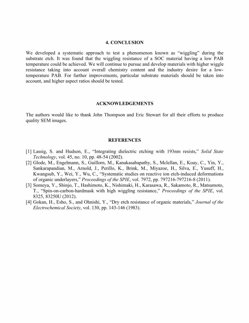
SOC1 was tested on three different days and gave the same result of no wiggling behavior with an aspect ratio greater than 5. SOC2 displayed the same wiggle behavior witnessed in the control. In an effort to increase the aspect ratio to further test SOC1’s resistance to the wiggle etch, the SOC lines were thinned by over-etching beyond the SOC recipe. This testing was possible because some Si-HM still remained on top of the lines. Thus, doing a longer etch would decrease the sidewall, creating a thinner line. The longer SOC etch to thin the lines, and thereby create a larger aspect ratio, was also performed on the control, SOC3. Figures 14 and 15 show the results of the longer SOC etch.
Figure 14: SEM photo of SOC1, aspect ratio: ~ 6.25.
Figure 15: SEM photo of SOC3, control
In Figure 14 the aspect ratio of the lines standing is ~ 6.25, with a line width of ~ 40 nm and a height of ~ 250 nm. This proves that SOC1, a material with a low PAB temperature of 225°C, can withstand the substrate etch successfully and is resistant to wiggling. Also the SOC1 material is spin bowl compatible and is easily removed with standard developer solution, even after undergoing all of the SOC RIE.
4. CONCLUSION We developed a systematic approach to test a phenomenon known as “wiggling” during the substrate etch. It was found that the wiggling resistance of a SOC material having a low PAB temperature could be achieved. We will continue to pursue and develop materials with higher wiggle resistance taking into account overall chemistry content and the industry desire for a low-temperature PAB. For further improvements, particular substrate materials should be taken into account, and higher aspect ratios should be tested.
ACKNOWLEDGEMENTS The authors would like to thank John Thompson and Eric Stewart for all their efforts to produce quality SEM images.
REFERENCES [1] Lassig, S. and Hudson, E., “Integrating dielectric etching with 193nm resists,” Solid State
Technology, vol. 45, no. 10, pp. 48-54 (2002). [2] Glode, M., Engelmann, S., Guillorn, M., Kanakasabapathy, S., Mclellan, E., Koay, C., Yin, Y.,
Sankarapandian, M., Arnold, J., Perillo, K., Brink, M., Miyazoe, H., Silva, E., Yusuff, H., Kwangsub, Y., Wei, Y., Wu, C., “Systematic studies on reactive ion etch-induced deformations of organic underlayers,” Proceedings of the SPIE, vol. 7972, pp. 797216-797216-8 (2011).
[3] Someya, Y., Shinjo, T., Hashimoto, K., Nishimaki, H., Karasawa, R., Sakamoto, R., Matsumoto, T., “Spin-on-carbon-hardmask with high wiggling resistance,” Proceedings of the SPIE, vol. 8325, 83250U (2012).
[4] Gokan, H., Esho, S., and Ohnishi, Y., “Dry etch resistance of organic materials,” Journal of the Electrochemical Society, vol. 130, pp. 143-146 (1983).