EVAL6480H and EVAL6482H: high power microstepping motor drivers€¦ · April 2015 DocID025458 Rev...
31
April 2015 DocID025458 Rev 2 1/31 31 UM1685 User manual EVAL6480H and EVAL6482H: high power microstepping motor drivers Introduction The EVAL6480H and EVAL6482H are two demonstration boards based on L648x devices implementing a complete stepper motor driver for high power applications. They are designed to operate with a supply voltage ranging from 10.5 V to 85 V and mount eight STD25NF10 MOSFETs with a maximum current of 25 A r.m.s. . In combination with the STEVAL-PCC009V2 demonstration board and the SPINFamily evaluation tool, the boards provide a complete and easy to use evaluation environment allowing the user to investigate all the features of the L648x devices. Both the boards support the daisy chain configuration making them suitable for the evaluation of the devices in multi motor applications. www.st.com
Transcript of EVAL6480H and EVAL6482H: high power microstepping motor drivers€¦ · April 2015 DocID025458 Rev...

April 2015 DocID025458 Rev 2 1/31
31
UM1685User manual
EVAL6480H and EVAL6482H: high power microstepping motordrivers
Introduction
The EVAL6480H and EVAL6482H are two demonstration boards based on L648x devices implementing a complete stepper motor driver for high power applications. They are designed to operate with a supply voltage ranging from 10.5 V to 85 V and mount eight STD25NF10 MOSFETs with a maximum current of 25 A r.m.s..
In combination with the STEVAL-PCC009V2 demonstration board and the SPINFamily evaluation tool, the boards provide a complete and easy to use evaluation environment allowing the user to investigate all the features of the L648x devices. Both the boards support the daisy chain configuration making them suitable for the evaluation of the devices in multi motor applications.
www.st.com

Contents UM1685
2/31 DocID025458 Rev 2
Contents
1 Boards description . . . . . . . . . . . . . . . . . . . . . . . . . . . . . . . . . . . . . . . . . . 5
1.1 EVAL6480H . . . . . . . . . . . . . . . . . . . . . . . . . . . . . . . . . . . . . . . . . . . . . . . . 5
1.2 EVAL6482H . . . . . . . . . . . . . . . . . . . . . . . . . . . . . . . . . . . . . . . . . . . . . . . 14
2 Evaluation environment setup . . . . . . . . . . . . . . . . . . . . . . . . . . . . . . . . 23
3 Device configuration . . . . . . . . . . . . . . . . . . . . . . . . . . . . . . . . . . . . . . . . 24
3.1 Voltage mode driving (EVAL6480H) . . . . . . . . . . . . . . . . . . . . . . . . . . . . . 24
3.2 Advanced current control (EVAL6482H) . . . . . . . . . . . . . . . . . . . . . . . . . 25
3.3 Gate drivers . . . . . . . . . . . . . . . . . . . . . . . . . . . . . . . . . . . . . . . . . . . . . . . 25
3.4 Overcurrent and stall detection thresholds . . . . . . . . . . . . . . . . . . . . . . . . 26
3.5 Speed profile . . . . . . . . . . . . . . . . . . . . . . . . . . . . . . . . . . . . . . . . . . . . . . 26
4 Sensing resistors of the EVAL6482H . . . . . . . . . . . . . . . . . . . . . . . . . . 27
5 How to change the supply configuration of the board . . . . . . . . . . . . 28
6 Daisy chaining . . . . . . . . . . . . . . . . . . . . . . . . . . . . . . . . . . . . . . . . . . . . . 29
7 Revision history . . . . . . . . . . . . . . . . . . . . . . . . . . . . . . . . . . . . . . . . . . . 30

DocID025458 Rev 2 3/31
UM1685 List of tables
31
List of tables
Table 1. EVAL6480H - electrical specifications . . . . . . . . . . . . . . . . . . . . . . . . . . . . . . . . . . . . . . . . . 5Table 2. EVAL6480H - jumper and connector description . . . . . . . . . . . . . . . . . . . . . . . . . . . . . . . . . 6Table 3. EVAL6480H - master SPI connector pinout (J3) . . . . . . . . . . . . . . . . . . . . . . . . . . . . . . . . . 6Table 4. EVAL6480H - slave SPI connector pinout (J4) . . . . . . . . . . . . . . . . . . . . . . . . . . . . . . . . . . . 7Table 5. EVAL6480H - bill of material. . . . . . . . . . . . . . . . . . . . . . . . . . . . . . . . . . . . . . . . . . . . . . . . 10Table 6. EVAL6482H - electrical specifications . . . . . . . . . . . . . . . . . . . . . . . . . . . . . . . . . . . . . . . . 14Table 7. EVAL6482H - jumper and connector description . . . . . . . . . . . . . . . . . . . . . . . . . . . . . . . . 15Table 8. EVAL6482H - master SPI connector pinout (J3) . . . . . . . . . . . . . . . . . . . . . . . . . . . . . . . . 15Table 9. EVAL6482H - slave SPI connector pinout (J4) . . . . . . . . . . . . . . . . . . . . . . . . . . . . . . . . . . 16Table 10. EVAL6482H - bill of material. . . . . . . . . . . . . . . . . . . . . . . . . . . . . . . . . . . . . . . . . . . . . . . . 19Table 11. VCC supply configurations . . . . . . . . . . . . . . . . . . . . . . . . . . . . . . . . . . . . . . . . . . . . . . . . . 28Table 12. VREG supply configurations. . . . . . . . . . . . . . . . . . . . . . . . . . . . . . . . . . . . . . . . . . . . . . . . 28Table 13. VDD supply configurations . . . . . . . . . . . . . . . . . . . . . . . . . . . . . . . . . . . . . . . . . . . . . . . . . 29Table 14. Document revision history . . . . . . . . . . . . . . . . . . . . . . . . . . . . . . . . . . . . . . . . . . . . . . . . . 30

List of figures UM1685
4/31 DocID025458 Rev 2
List of figures
Figure 1. EVAL6480H - jumper and connector location. . . . . . . . . . . . . . . . . . . . . . . . . . . . . . . . . . . . 5Figure 2. EVAL6480H - schematic part 1/2 . . . . . . . . . . . . . . . . . . . . . . . . . . . . . . . . . . . . . . . . . . . . . 8Figure 3. EVAL6480H - schematic part 2/2 . . . . . . . . . . . . . . . . . . . . . . . . . . . . . . . . . . . . . . . . . . . . . 9Figure 4. EVAL6480H - layout (top layer) . . . . . . . . . . . . . . . . . . . . . . . . . . . . . . . . . . . . . . . . . . . . . 12Figure 5. EVAL6480H - layout (inner layer 2) . . . . . . . . . . . . . . . . . . . . . . . . . . . . . . . . . . . . . . . . . . 12Figure 6. EVAL6480H - layout (inner layer 3) . . . . . . . . . . . . . . . . . . . . . . . . . . . . . . . . . . . . . . . . . . 13Figure 7. EVAL6480H - layout (bottom layer ) . . . . . . . . . . . . . . . . . . . . . . . . . . . . . . . . . . . . . . . . . . 13Figure 8. EVAL6482H - jumper and connector location. . . . . . . . . . . . . . . . . . . . . . . . . . . . . . . . . . . 14Figure 9. EVAL6482H - schematic part 1/2 . . . . . . . . . . . . . . . . . . . . . . . . . . . . . . . . . . . . . . . . . . . . 17Figure 10. EVAL6482H - schematic part 2/2 . . . . . . . . . . . . . . . . . . . . . . . . . . . . . . . . . . . . . . . . . . . . 18Figure 11. EVAL6482H - layout (top layer) . . . . . . . . . . . . . . . . . . . . . . . . . . . . . . . . . . . . . . . . . . . . . 21Figure 12. EVAL6482H - layout (inner layer 2) . . . . . . . . . . . . . . . . . . . . . . . . . . . . . . . . . . . . . . . . . . 21Figure 13. EVAL6482H - layout (inner layer 3) . . . . . . . . . . . . . . . . . . . . . . . . . . . . . . . . . . . . . . . . . . 22Figure 14. EVAL6482H - layout (bottom layer) . . . . . . . . . . . . . . . . . . . . . . . . . . . . . . . . . . . . . . . . . . 22
DocID025458 Rev 2 5/31
UM1685 Boards description
31
1 Boards description
1.1 EVAL6480H
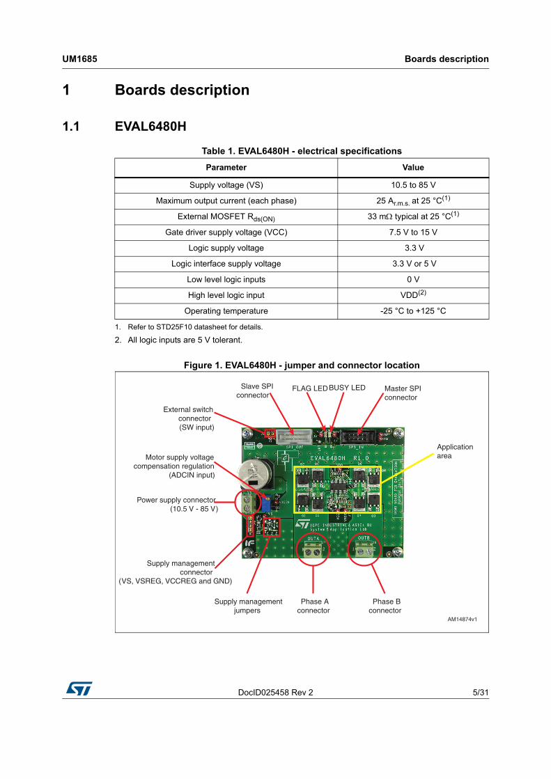
Figure 1. EVAL6480H - jumper and connector location
Table 1. EVAL6480H - electrical specifications
Parameter Value
Supply voltage (VS) 10.5 to 85 V
Maximum output current (each phase) 25 Ar.m.s. at 25 °C(1)
1. Refer to STD25F10 datasheet for details.
External MOSFET Rds(ON) 33 m typical at 25 °C(1)
Gate driver supply voltage (VCC) 7.5 V to 15 V
Logic supply voltage 3.3 V
Logic interface supply voltage 3.3 V or 5 V
Low level logic inputs 0 V
High level logic input VDD(2)
2. All logic inputs are 5 V tolerant.
Operating temperature -25 °C to +125 °C
FLAG LED
Supply managementjumpers
Phase Aconnector
Phase Bconnector
Master SPIconnector
Applicationarea
Slave SPIconnector
External switch connector (SW input)
Motor supply voltagecompensation regulation
(ADCIN input)
Power supply connector(10.5 V - 85 V)
Supply managementconnector
(VS, VSREG, VCCREG and GND)
BUSY LED
AM14874v1

Boards description UM1685
6/31 DocID025458 Rev 2
Table 2. EVAL6480H - jumper and connector description
Name Type Function
J5 Power supply Main supply voltage
J7 Power output Power bridge A outputs
J8 Power output Power bridge B outputs
J6 Power supply Integrated voltage regulator inputs
J3 SPI Master SPI connector
J4 SPI Slave SPI connector
JP1 Jumper VS to VSREG jumper
JP2 Jumper VSREG to VCC jumper
JP3 Jumper VCC to VCCREG jumper
JP4 Jumper VCCREG to VREG jumper
JP5 Jumper VREG to VDD jumper
JP6 Jumper VDD to 3.3 V from SPI connector jump
JP7 Jumper Daisy chain termination jumper
JP8 Jumper STBY to VS pull-up jumper
TP8 (BUSY/SYNC) Jumper BUSY/SYNC output test point
Table 3. EVAL6480H - master SPI connector pinout (J3)
Pin number Type Description
1 Open drain output L6480 BUSY output
2 Open drain output L6480 FLAG output
3 Ground Ground
4 Supply EXT_VDD (can be used as external logic power supply)
5 Digital outputSPI master IN slave OUT signal (connected to the L6480 SDO output through daisy chain termination jumper JP7)
6 Digital input SPI serial clock signal (connected to L6480 CK input)
7 Digital inputSPI master OUT slave IN signal (connected to L6480 SDI
input)
8 Digital input SPI slave select signal (connected to L6480 CS input)
9 Digital input L6480 step-clock input
10 Digital input L6480 standby/reset input

DocID025458 Rev 2 7/31
UM1685 Boards description
31
Table 4. EVAL6480H - slave SPI connector pinout (J4)
Pin number Type Description
1 Open drain output L6480 BUSY output
2 Open drain output L6480 FLAG output
3 Ground Ground
4 Supply EXT_VDD (can be used as external logic power supply)
5 Digital output SPI master IN slave OUT signal (connected to pin 5 of J3)
6 Digital input SPI serial clock signal (connected to L6480 CK input)
7 Digital input SPI master OUT slave IN signal (connected to L6480 SDO output)
8 Digital input SPI slave select signal (connected to L6480 CS input)
9 Digital input L6480 step-clock input
10 Digital input L6480 standby/reset input
Boards description UM1685
8/31 DocID025458 Rev 2
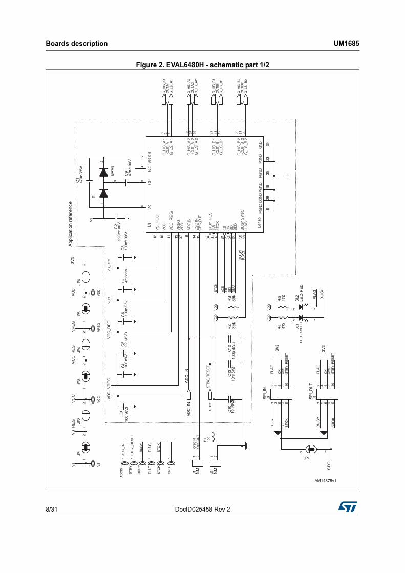
Figure 2. EVAL6480H - schematic part 1/2
SP
I_IN
SP
I_O
UT
App
licat
ion
refe
renc
e
OS
CIN
OS
CO
UT
ST
CK
nCS
CK
SD
IS
DO
BU
SY
F LA
G
nCS
CK
SD
I
BU
SY
BU
SY
FLA
G
FLA
G
nCS
CK
SD
O
ST
BY
_RE
SE
T
ST
BY
_RE
SE
TST
CK
ST
CK
FLA
G
BU
SY
AD
C_
IN
STBY
_RE
SE
T
BU
SY
ST
BY
_RE
SE
T
FLA
G
ST
CK
AD
C_I
N
G_H
S_A
1
G_L
S_A
1
G_H
S_A
2
G_L
S_A
2
G_H
S_B
1
G_H
S_B
2
G_L
S_B
2
G_L
S_B
1
OU
TA
1
OU
TA
2
OU
TB
1
OU
TB
2
ST
BY
AD
C_
IN
VS
VS
_RE
GV
CC
VC
C_R
EG
VR
EG
VD
D
3V3
3V3
VD
DV
DD
VD
DV
DD
3V3
VS
VS
_RE
GV
CC
VC
C_R
EG
VR
EG
VD
D
AD
CIN
1C
522
u/6
V3
JP1
12
VC
C
1
ST
BY
1
U1
L648
0
G_L
S_A
11
OU
T _A
12
G_H
S_A
13
G_L
S_A
238
OU
T_A
237
G_H
S_A
23 6
OU
T_B
118
G_L
S_B
119
OU
T_B
221
G_L
S_B
220
G_H
S_B
117
G_H
S_B
222
PGN
D
2 3
PGN
D
35
AGN
D
16
DG
ND
2 9
V S
6
PGN
D
8
VS
_RE
G12
VCC
10
VC
C_R
EG
11
VR
EG
13
VBO
OT
7
CP9
AD
C_IN
5V
DD
27
STB
Y _R
ES
34
CS
24
SDO
28C
K2 5
SD
I26
OS
C_IN
1 4
OS
C_O
UT
15
SW
33ST C
K32
BU
SY_S
YNC
30
FLA
G31
GN
D
39
N.C
.4
GN
D1
JP3
12
C9
47n
/100
V
C2
220
n/10
0V
JP2
12
J 2 N.M
.1 2 JP7
12
R4 470
C8
100
n/10
0V
C1
470
n/2
5V
J 1 N.M
.1 2
VD
D
1
VS
1
R1
100
C13
10n
/ 6V
3
JP5
12
VR
EG
1
R3
39k
BU
SY
1
C12
100p
/ 6V
3
C7
470n
/ 25V
J31
23
45
67
89
10
J41
23
45
67
89
1 0
JP4
12
JP6
12
C6
100
n/ 2
5V
ST
CK
1
C10
10n
/6V3
R2 39
k
D1
BA
V9
12
3
DL1
LED
- A
MB
ER
2 1
R5
470
C4
100
n/4V
C3
100
n/6V
3
DL2
LED
- RE
D
2 1
FLA
G1
AM14875v1

DocID025458 Rev 2 9/31
UM1685 Boards description
31
Figure 3. EVAL6480H - schematic part 2/2
OP
TIO
N
VS
VS
_RE
GV
CC
_RE
GG
ND
OU
TA
12
OU
TB
12
GN
DVS
App
licat
ion
refe
renc
e
G_H
S_B
2
G_L
S_B
2
G_H
S_B
1
G_L
S_B
1
G_H
S_A
1
G_L
S_A
1
G_H
S_A
2
G_L
S_A
2
OU
TA1
OU
TA2
OU
TB1
OU
TB
2
ST
BY
AD
C_I
N
VSV
SV
S_R
EG
VC
C_R
EG
VS
VS
VS
_RE
GV
SV
DD
VS
VS
JP8
12
Q1
S TD
25N
F10
1
4 3
Q4
STD
25N
F10
1
4
3
C15
220
n/1
00V
D2
BZX5
85- B
3V3
Q5
STD
25N
F10
1
4 3
J8
12
+C
11A
220u
/100
V
Q8
ST
D25
NF
101
4 3
Q2
STD
25N
F10
1
43
C14
220n
/100
V
J 6 N.M
.
1 2 3 4
R9
N.M
.
+C
1122
0u
/100
V
R7
100
k/0
.125
W
Q6
STD
25N
F 10
1
43
R6
100k
/0.1
25W
J5
12
R8
50k/
0.125
W
13
2
Q3
STD
25N
F10
1
4 3
J7
12
Q7
ST
D25
NF
101
4 3
D3
BZX5
85- B
3V6
AM14880v1
Boards description UM1685
10/31 DocID025458 Rev 2
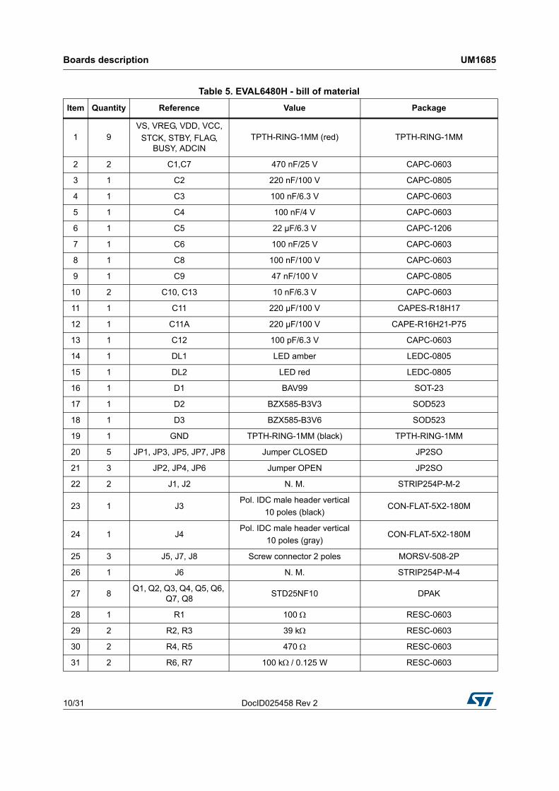
Table 5. EVAL6480H - bill of material
Item Quantity Reference Value Package
1 9VS, VREG, VDD, VCC,
STCK, STBY, FLAG, BUSY, ADCIN
TPTH-RING-1MM (red) TPTH-RING-1MM
2 2 C1,C7 470 nF/25 V CAPC-0603
3 1 C2 220 nF/100 V CAPC-0805
4 1 C3 100 nF/6.3 V CAPC-0603
5 1 C4 100 nF/4 V CAPC-0603
6 1 C5 22 µF/6.3 V CAPC-1206
7 1 C6 100 nF/25 V CAPC-0603
8 1 C8 100 nF/100 V CAPC-0603
9 1 C9 47 nF/100 V CAPC-0805
10 2 C10, C13 10 nF/6.3 V CAPC-0603
11 1 C11 220 µF/100 V CAPES-R18H17
12 1 C11A 220 µF/100 V CAPE-R16H21-P75
13 1 C12 100 pF/6.3 V CAPC-0603
14 1 DL1 LED amber LEDC-0805
15 1 DL2 LED red LEDC-0805
16 1 D1 BAV99 SOT-23
17 1 D2 BZX585-B3V3 SOD523
18 1 D3 BZX585-B3V6 SOD523
19 1 GND TPTH-RING-1MM (black) TPTH-RING-1MM
20 5 JP1, JP3, JP5, JP7, JP8 Jumper CLOSED JP2SO
21 3 JP2, JP4, JP6 Jumper OPEN JP2SO
22 2 J1, J2 N. M. STRIP254P-M-2
23 1 J3Pol. IDC male header vertical
10 poles (black)CON-FLAT-5X2-180M
24 1 J4Pol. IDC male header vertical
10 poles (gray)CON-FLAT-5X2-180M
25 3 J5, J7, J8 Screw connector 2 poles MORSV-508-2P
26 1 J6 N. M. STRIP254P-M-4
27 8Q1, Q2, Q3, Q4, Q5, Q6,
Q7, Q8STD25NF10 DPAK
28 1 R1 100 RESC-0603
29 2 R2, R3 39 k RESC-0603
30 2 R4, R5 470 RESC-0603
31 2 R6, R7 100 k/ 0.125 W RESC-0603

DocID025458 Rev 2 11/31
UM1685 Boards description
31
32 1 R8 33 k/ 0.125 W TRIMM-100X50X110-64W
33 1 R9 N. M. RESC-0603
34 1 U1 L6480 HTSSOP050P-660X110-38-EP
Table 5. EVAL6480H - bill of material (continued)
Item Quantity Reference Value Package

Boards description UM1685
12/31 DocID025458 Rev 2
Figure 4. EVAL6480H - layout (top layer)
Figure 5. EVAL6480H - layout (inner layer 2)

DocID025458 Rev 2 13/31
UM1685 Boards description
31
Figure 6. EVAL6480H - layout (inner layer 3)
Figure 7. EVAL6480H - layout (bottom layer )

Boards description UM1685
14/31 DocID025458 Rev 2
1.2 EVAL6482H
Figure 8. EVAL6482H - jumper and connector location
Table 6. EVAL6482H - electrical specifications
Parameter Value
Supply voltage (VS) 10.5 to 85 V
Maximum output current (each phase) 6 Ar.m.s. at 25 °C(1)
1. Limited by the mounted sensing resistors.
External MOSFET Rds(ON) 33 m typical at 25 °C(2)
2. Refer to STD25NF10 datasheet for details.
Gate driver supply voltage (VCC) 7.5 V to 15 V
Logic supply voltage 3.3 V
Logic interface supply voltage 3.3 V or 5 V
Low level logic input 0 V
High level logic input VDD(3)
3. All logic inputs are 5 V tolerant.
Operating temperature -25 °C to +125 °C
FLAG LED
Supply managementjumpers
Phase Aconnector
Phase Bconnector
Master SPIconnector
Applicationarea
Slave SPIconnector
External switch connector (SW input)
ADCIN input
Power supply connector(10.5 V - 85 V)
Supply managementconnector
(VS, VSREG, VCCREG and GND)
BUSY LED
AM15181v1

DocID025458 Rev 2 15/31
UM1685 Boards description
31
Table 7. EVAL6482H - jumper and connector description
Name Type Function
J5 Power supply Main supply voltage
J7 Power output Power bridge A outputs
J8 Power output Power bridge B outputs
J6 Power supply Integrated voltage regulator inputs
J3 SPI Master SPI connector
J4 SPI Slave SPI connector
JP1 Jumper VS to VSREG jumper
JP2 Jumper VSREG to VCC jumper
JP3 Jumper VCC to VCCREG jumper
JP4 Jumper VCCREG to VREG jumper
JP5 Jumper VREG to VDD jumper
JP6 Jumper VDD to 3.3 V from SPI connector jumper
JP7 Jumper Daisy chain termination jumper
JP8 Jumper STBY to VS pull-up jumper
Table 8. EVAL6482H - master SPI connector pinout (J3)
Pin number Type Description
1 Open drain output L6482 BUSY output
2 Open drain output L6482 FLAG output
3 Ground Ground
4 Supply EXT_VDD (can be used as external logic power supply)
5 Digital outputSPI master IN slave OUT signal (connected to the L6482 SDO
output through daisy chain termination jumper JP7)
6 Digital input SPI serial clock signal (connected to L6482 CK input)
7 Digital input SPI master OUT slave IN signal (connected to L6482 SDI input)
8 Digital input SPI slave select signal (connected to L6482 CS input)
9 Digital input L6482 step-clock input
10 Digital input L6482 standby/reset input

Boards description UM1685
16/31 DocID025458 Rev 2
Table 9. EVAL6482H - slave SPI connector pinout (J4)
Pin number Type Description
1 Open drain output L6482 BUSY output
2 Open drain output L6482 FLAG output
3 Ground Ground
4 Supply EXT_VDD (can be used as external logic power supply)
5 Digital output SPI master IN slave OUT signal (connected to pin 5 of J3)
6 Digital input SPI serial clock signal (connected to L6482 CK input)
7 Digital input SPI master OUT slave IN signal (connected to L6482 SDO output)
8 Digital input SPI slave select signal (connected to L6482 CS input)
9 Digital input L6482 step-clock input
10 Digital input L6482 standby/reset input

DocID025458 Rev 2 17/31
UM1685 Boards description
31
Figure 9. EVAL6482H - schematic part 1/2A
pplic
atio
n re
fere
nce
SP
I_IN
SP
I_O
UT
VS
VC
CV
RE
GV
DD
AD
C_I
N
STB
Y
BU
SY
FLA
G
STC
K
GN
D
BU
SY
FLA
G
SD
O
ST
BY
_RE
SE
T
ST
BY
_RE
SE
TS
TC
K
ST
CK
nCS
CK
AD
C_I
N
ST
BY
_RE
SE
T
SD
I
BU
SY
BU
SY
FLA
G
FLA
G
nCS
CK
BU
SY
ST
BY
_RE
SE
T
FLA
G
ST
CK
AD
C_I
N OS
CIN
FLA
G
OS
CO
UT
BU
SYS
TC
K
nCS
CK
SD
IS
DO
BU
SY
FLA
G
G_L
S_B
1
OU
TA
1
OU
TA
2
OU
TB
1
OU
TB
2
ST
BY
G_H
S_A
1
G_L
S_A
1
AD
C_I
NG
_HS
_A2
G_L
S_A
2
G_H
S_B
1
G_H
S_B
2
G_L
S_B
2
SE
NS
EA
SE
NS
EB
3V3
3V3
VS
VS
_RE
GV
CC
VC
C_R
EG
VR
EG
VD
D
VD
DV
DD
VD
DV
DD
3V3
VS
VS
_RE
GV
CC
VC
C_R
EG
VR
EG
VD
D
R5
470
FLA
G1
R3
39k
ST
BY
1C
410
0n/4
V
C3
100n
/6V
3
J31
23
45
67
89
10
VC
C
1
JP1
12
R1
100
R4 47
0
C13
10n/
6V3
R2 39
k
JP3
12
VR
EG
1
C2
220n
/100
VC
522
u/6V
3
DL1
LED
- A
MB
ER
21
JP2
12
J2 N.M
.1 2
GN
D1
C8
100n
/100
V
J41
23
45
67
89
10
BU
SY
1
D1
BA
V99
12
3
DL2
LED
- R
ED
21
JP5
12
C7
470n
/25V
JP7
12
JP6
12
VD
D
1
J1 N.M
.1 2
C9
47n/
100V
JP4
12
U1
L648
2
G_L
S_A
11
OU
T_A
12
G_H
S_A
13
G_L
S_A
238
OU
T_A
237
G_H
S_A
236
OU
T_B
118
G_L
S_B
119
OU
T_B
221
G_L
S_B
220
G_H
S_B
117
G_H
S_B
222
SE
NS
EB
23
SE
NS
EA
35
AG
ND
16
DG
ND
29
VS6
PG
ND
8
VS
_RE
G12
VC
C10
VC
C_R
EG
11
VR
EG
13
VB
OO
T
7
CP9
AD
C_I
N5
VD
D27
ST
BY
_RE
S34
CS
24
SD
O28
CK
25
SD
I26
OS
C_I
N14
OS
C_O
UT
15
SW
33
ST
CK
32
BU
SY
_SY
NC
30
FLA
G31
GN
D
39
ST
CK
1
C10
10n/
6V3
AD
CIN
1
C1
470n
/25V
C12
100p
/6V
3
C6
100n
/25V
VS
1
AM15182v1

Boards description UM1685
18/31 DocID025458 Rev 2
Figure 10. EVAL6482H - schematic part 2/2
App
licat
ion
refe
renc
e
OP
TIO
N
VS
VS
_RE
GV
CC
_RE
GG
ND
OU
TA
12
OU
TB
12
GN
DVS
G_H
S_B
2
G_L
S_B
2
G_H
S_B
1
G_L
S_B
1
G_H
S_A
1
G_L
S_A
1
G_H
S_A
2
G_L
S_A
2
ST
BY
OU
TA
1O
UT
A2
OU
TB
1O
UT
B2
AD
C_I
N
SE
NS
EA
SE
NS
EB
VS
VS
VD
D
VS
VS
VS
_RE
GV
CC
_RE
GV
S
VS
VS
_RE
GV
S
Q8
ST
D25
NF
101
4 3Q
4S
TD
25N
F10
14 3
+C
1122
0u/1
00V
C15
220n
/100
V
+C
11A
220u
/100
V
D2
BZ
X58
5-B
3V3
R7
100k
/0.1
25W
R19
0R1/
2WR
180R
1/2W
R17
50k/
0.12
5W
13
2
Q1
ST
D25
NF
101
4 3
R9 N.M
.
Q6
ST
D25
NF
101
4 3
J5
12
Q3
ST
D25
NF
101
4 3
R6
100k
/0.1
25W
J6 N.M
.
1 2 3 4
R21
0R1/
2W
Q5
ST
D25
NF
101
4 3
JP8
12
Q2
ST
D25
NF
101
4 3
J812
R20
0R1/
2W
C14
220n
/100
V
J7
12
D3
BZ
X58
5-B
3V6
Q7
ST
D25
NF
101
4 3
AM15183v1
DocID025458 Rev 2 19/31
UM1685 Boards description
31
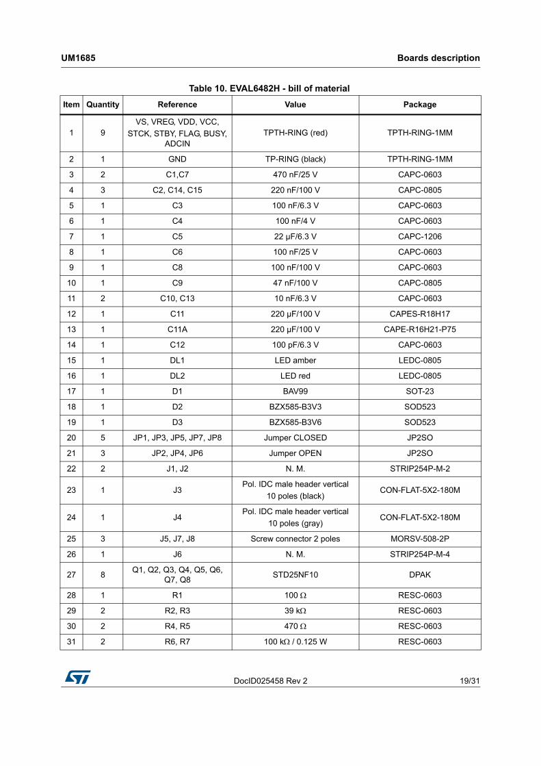
Table 10. EVAL6482H - bill of material
Item Quantity Reference Value Package
1 9VS, VREG, VDD, VCC,
STCK, STBY, FLAG, BUSY, ADCIN
TPTH-RING (red) TPTH-RING-1MM
2 1 GND TP-RING (black) TPTH-RING-1MM
3 2 C1,C7 470 nF/25 V CAPC-0603
4 3 C2, C14, C15 220 nF/100 V CAPC-0805
5 1 C3 100 nF/6.3 V CAPC-0603
6 1 C4 100 nF/4 V CAPC-0603
7 1 C5 22 µF/6.3 V CAPC-1206
8 1 C6 100 nF/25 V CAPC-0603
9 1 C8 100 nF/100 V CAPC-0603
10 1 C9 47 nF/100 V CAPC-0805
11 2 C10, C13 10 nF/6.3 V CAPC-0603
12 1 C11 220 µF/100 V CAPES-R18H17
13 1 C11A 220 µF/100 V CAPE-R16H21-P75
14 1 C12 100 pF/6.3 V CAPC-0603
15 1 DL1 LED amber LEDC-0805
16 1 DL2 LED red LEDC-0805
17 1 D1 BAV99 SOT-23
18 1 D2 BZX585-B3V3 SOD523
19 1 D3 BZX585-B3V6 SOD523
20 5 JP1, JP3, JP5, JP7, JP8 Jumper CLOSED JP2SO
21 3 JP2, JP4, JP6 Jumper OPEN JP2SO
22 2 J1, J2 N. M. STRIP254P-M-2
23 1 J3Pol. IDC male header vertical
10 poles (black)CON-FLAT-5X2-180M
24 1 J4Pol. IDC male header vertical
10 poles (gray)CON-FLAT-5X2-180M
25 3 J5, J7, J8 Screw connector 2 poles MORSV-508-2P
26 1 J6 N. M. STRIP254P-M-4
27 8Q1, Q2, Q3, Q4, Q5, Q6,
Q7, Q8STD25NF10 DPAK
28 1 R1 100 RESC-0603
29 2 R2, R3 39 k RESC-0603
30 2 R4, R5 470 RESC-0603
31 2 R6, R7 100 k/ 0.125 W RESC-0603

Boards description UM1685
20/31 DocID025458 Rev 2
32 1 R9 N. M. RESC-0603
33 1 R17 50 k/ 0.125 W TRIMM-100X50X110-64W
34 4 R18, R19, R20, R21 0.1 /2W RESC-2010
35 1 U1 L6482 HTSSOP050P-660X110-38-EP
Table 10. EVAL6482H - bill of material (continued)
Item Quantity Reference Value Package
DocID025458 Rev 2 21/31
UM1685 Boards description
31
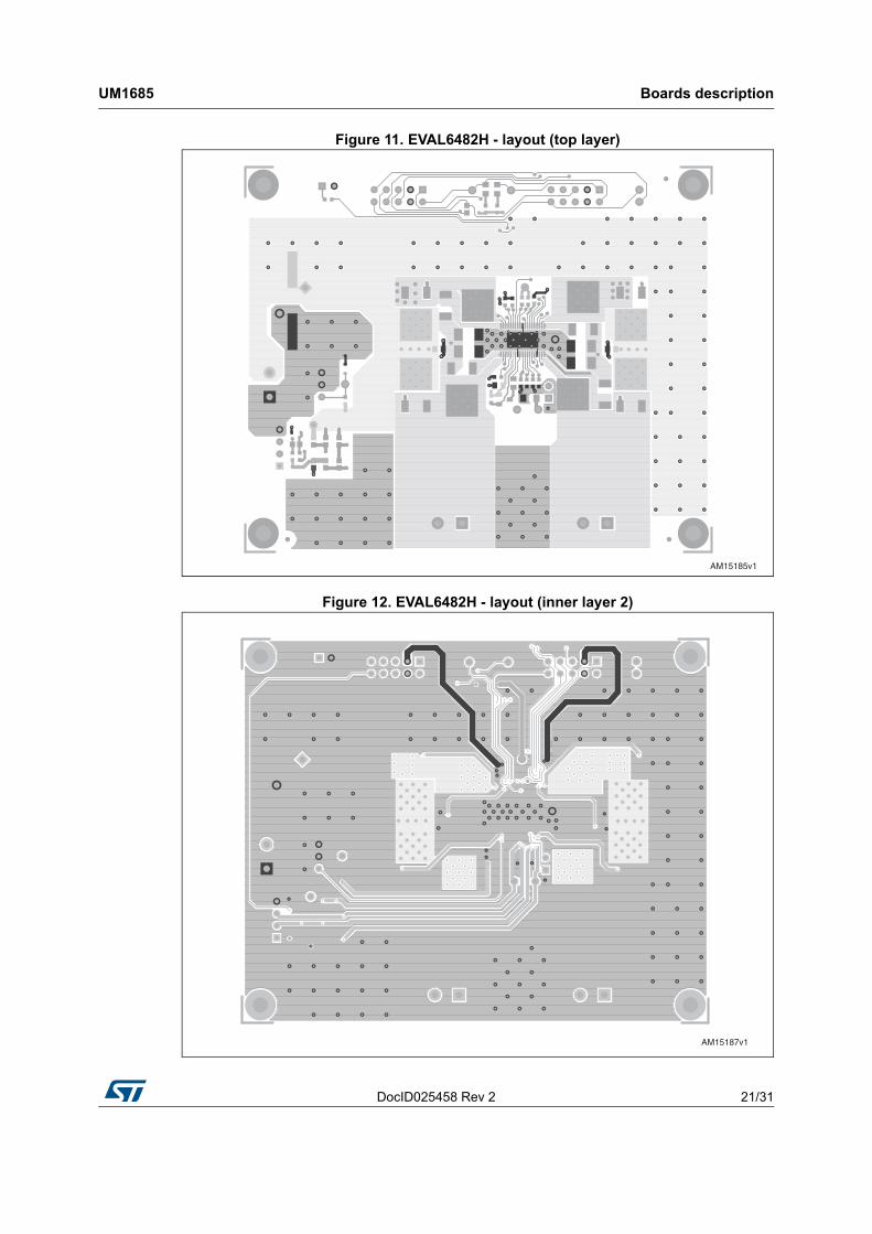
Figure 11. EVAL6482H - layout (top layer)
Figure 12. EVAL6482H - layout (inner layer 2)
AM15185v1
AM15187v1

Boards description UM1685
22/31 DocID025458 Rev 2
Figure 14. EVAL6482H - layout (bottom layer)
Figure 13. EVAL6482H - layout (inner layer 3)
AM15188v1
AM15189v1

DocID025458 Rev 2 23/31
UM1685 Evaluation environment setup
31
2 Evaluation environment setup
The evaluation environment is composed by:
One or more EVAL6480H or EVAL6482H device
One STEVAL-PCC009V2 demonstration board
A USB cable
A stepper motor with a small mechanical load (unloaded stepper motors suffer of strong resonance issues)
A power supply with an output voltage within the operative range of the evaluation board
A PC with a Microsoft© Windows® 7 or Windows XP operating system and with a free USB port
The SPINFamily evaluation tool (the last version can be downloaded from the STMicroelectronics® website).
In order to start using the evaluation environment the following steps are required:
1. Install the SPINFamily evaluation tool.
2. Start the SPINFamily evaluation tool (by default it is in Start menu > All programs > STMicroelectronics > SPINFamily Evaluation Tool).
3. Select the proper device when requested by the application.
4. Plug the STEVAL-PCC009V2 demonstration board to a free USB port.
5. Wait a few seconds for board initialization.
6. Connect the SPI_IN connector (black) of the demonstration board to the 10-pin connector of the STEVAL-PCC009V2 board using the provided cable. For connecting more devices to the same board, please consult Section 6: Daisy chaining on page 29.
7. Power up the demonstration boards. The FLAG LED should turn on.
8. Click on the button with the USB symbol to connect the STEVAL-PCC009V2 board to the PC and initialize the evaluation environment.The application automatically identifies the number of demonstration boards connected.
9. The evaluation environment is ready.
Before start working with the demonstration board, the device must be configured according to the indications described in Section 3: Device configuration.
Warning: Important - the device configuration is mandatory. The default configuration is not operative.
Device configuration UM1685
24/31 DocID025458 Rev 2
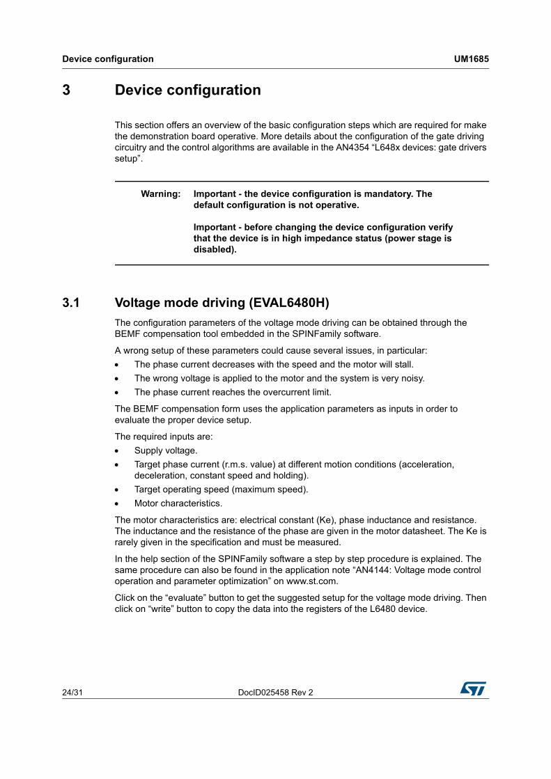
3 Device configuration
This section offers an overview of the basic configuration steps which are required for make the demonstration board operative. More details about the configuration of the gate driving circuitry and the control algorithms are available in the AN4354 “L648x devices: gate drivers setup”.
Warning: Important - the device configuration is mandatory. The default configuration is not operative.
Important - before changing the device configuration verify that the device is in high impedance status (power stage is disabled).
3.1 Voltage mode driving (EVAL6480H)
The configuration parameters of the voltage mode driving can be obtained through the BEMF compensation tool embedded in the SPINFamily software.
A wrong setup of these parameters could cause several issues, in particular:
The phase current decreases with the speed and the motor will stall.
The wrong voltage is applied to the motor and the system is very noisy.
The phase current reaches the overcurrent limit.
The BEMF compensation form uses the application parameters as inputs in order to evaluate the proper device setup.
The required inputs are:
Supply voltage.
Target phase current (r.m.s. value) at different motion conditions (acceleration, deceleration, constant speed and holding).
Target operating speed (maximum speed).
Motor characteristics.
The motor characteristics are: electrical constant (Ke), phase inductance and resistance. The inductance and the resistance of the phase are given in the motor datasheet. The Ke is rarely given in the specification and must be measured.
In the help section of the SPINFamily software a step by step procedure is explained. The same procedure can also be found in the application note “AN4144: Voltage mode control operation and parameter optimization” on www.st.com.
Click on the “evaluate” button to get the suggested setup for the voltage mode driving. Then click on “write” button to copy the data into the registers of the L6480 device.

DocID025458 Rev 2 25/31
UM1685 Device configuration
31
3.2 Advanced current control (EVAL6482H)
The following configuration gives good results with most of motors:
Minimum ON time = 4 µs.
Minimum OFF time = 21 µs.
Max fast decay = 10 µs.
Max fast decay at step change = 16 µs.
Target switching time = 48 µs.
Predictive current control enabled.
The impact of the timing parameters are explained in the application note “AN4158: Peak current control with automatic decay adjustment and predictive current control: basics and setup” on www.st.com.
The target phase current is set through the TVAL registers. The TVAL determinates the reference voltage (i.e. the voltage drop on the sense resistors) corresponding to the peak of the current sine wave (microstepping operation):
Equation 1
Ipeak = TVAL_X / Rsense = TVAL_X / 0.05
The sensing resistors can be changed as described in Section 5: How to change the supply configuration of the board.
3.3 Gate drivers
The configuration of the gate driving circuitry depends on the external MOSFETs characteristics. The demonstration boards mount the STD25NF10 Power MOSFETs.
Warning: Important - a wrong gate driving setup may cause spurious overcurrent failures even if no load is connected to the power stage.
According to the STD25NF10 datasheet the total gate charge required to turn on the MOSFET is about 55 nC.
The charge supplied by the device at each commutation is equal to the gate current (Igate) multiplied by the controlled current time (tcc). With a gate current of 64 mA and a controller current time of 1000 ns, 64 nC are provided to the gate. The gate current can be changed in order to speed up or slow down the commutation speed (i.e. the slew rate of the power stage outputs); in this case the controlled current time should be changed accordingly.
The boards are designed to operate with a VCC voltage of 15 V, so the corresponding value for the integrated regulator should be set. The UVLO threshold should be 11 V.
At each commutation some voltage oscillations are generated. This noise could trigger the overcurrent protection. This event is avoided by adding a blanking time after each commutation.
A blanking time of 500 ns prevents the occurrence of spurious overcurrent detection in most operative conditions.

Device configuration UM1685
26/31 DocID025458 Rev 2
In conclusion the suggested configuration for the demonstration boards is following:
VCC value = 15 V.
UVLO threshold = 11 V (10 V on boot).
Gate current = 64 mA.
Controlled current time = 1 s.
Dead time = 250 ns.
Blanking time = 500 ns.
Turn OFF boost time = disabled.
3.4 Overcurrent and stall detection thresholds
The overcurrent protection and the stall detection (EVAL6480H only) are implemented by measuring the drain-source voltage of the MOSFETs, hence their value is a voltage and not a current.
The protection thresholds are set according to the voltage drop caused by the target triggering current on the MOSFET RdsON at the expected operating temperature (in fact this parameter increases with temperature).
During the preliminary stages of evaluation, the max. value of 1000 mV can be set for both protections. The default value of 281.25 mV has a good probability to trigger the overcurrent alarm.
Warning: Important - it is strongly discouraged to disable the overcurrent shutdown. It may result in critical failures.
3.5 Speed profile
The max. speed parameter is the maximum speed the motor will run. By default, it is about 1000 step/s. That means, if you send a command to run at 2000 step/s, the motor speed is limited at 1000 step/s.
This is an important safety feature in the final application, but not necessarily useful to evaluate the device performances. Setting the parameter to high values (e.g. 6000 step/s) allows evaluating the maximum speed which can be achieved by the application under test through the speed tracking command (Run), but it probably limits the possibility to use positioning commands (Move, GoTo, etc.).
The Full-step speed parameter indicates the speed at which the system switches from microstepping to full step operation.
In voltage mode driving devices (EVAL6480H), it is always recommended to operate in microstepping and not to switch to the full step. Hence, this parameter should be greater than the maximum speed.

DocID025458 Rev 2 27/31
UM1685 Sensing resistors of the EVAL6482H
31
4 Sensing resistors of the EVAL6482H
The output current range of the board is determined by the sensing resistors as indicated in Equation 2 and Equation 3:
Equation 2
Ipeak,min = 7.8 mV / Rsense
Equation 3
Ipeak,max = 1 V / Rsense
Where 7.8 mV and 1 V are the minimum and the maximum value of the TVAL registers.
However the actual output current is usually limited by the power rating of the sensing resistors:
Equation 4
Note: The power rating of the sensing resistor determining the maximum output current is 50% of the nominal one.
If the operative range resulting from the sensing resistors which are mounted on the board is not suitable for the application, it is possible to change these components in order to fit the requirements.
The sensing resistors should make the current control to operate with a peak reference voltage between 0.2 and 0.1 volts. This way the power dissipation on the sensing resistor is not excessive and the offset of the sensing circuitry does not affect the performance of the current control algorithm.
Equation 5
Rsense = 0.2 V / Ipeak
Iout l imitPd maxRsense------------------= (r.m.s. value)

How to change the supply configuration of the board UM1685
28/31 DocID025458 Rev 2
5 How to change the supply configuration of the board
The configuration of the supply voltages can be changed through the jumpers from J1 to J6 as listed in Table 11, Table 12 and Table 13.
Note: When the VCC voltage of 7.5 V is used, the charge pump diodes should be replaced with low-drop ones (suggested part BAR43SFILM). Otherwise the resulting boot voltage could be lower than the respective UVLO threshold and the device is not operative.
When the VSREG pin is not shorted to the VS (JP1 is open) particular care must be taken in order to avoid that the VBOOT voltage falls below the VSREG one (e.g. VS is floating and VSREG is supplied). In this case the internal ESD diode is turned on and the device could be damaged.
Adding a low drop diode between the VSREG and VS protects the internal ESD diode from this event (the diodes of the charge pump must also be low drop type).
When the VCCREG pin is not shorted to the VCC (JP3 is open) particular care must be taken in order to avoid that the VCC voltage falls below the VCCREG one. In this case the internal ESD diode is turned on and the device could be damaged.
Adding a low drop diode between the VCCREG and VCC protects the internal ESD diode from this event.
Table 11. VCC supply configurations
Configuration JP1 JP2 VSREG range Notes
Internally generated from VS
Closed Open VCC + 3 V ÷ 85 VDefault.
VCC value is determined by the internal regulator configuration.
Internally generated from a voltage source different
from VS
Open Open VCC + 3 V ÷ VS
VCC value is determined by the internal regulator configuration.
External protection diode could be required (see following text below table).
Externally supplied (equal to VSREG)
Open Closed 7.5 V ÷ 15 VExternal protection diode could be required
(see following text below table).
Table 12. VREG supply configurations
Configuration JP3 JP4 VCCREG range Notes
Internally generated from VCC
Closed Open VCC Default.
Internally generated from a voltage source different
from VCC
Open Open 6.3 V ÷ VCCExternal protection diode could be required
(see following text below table).
Externally supplied (equal to VCCREG)
Open Closed 3.3 VExternal protection diode could be required
(see following text below table).
DocID025458 Rev 2 29/31
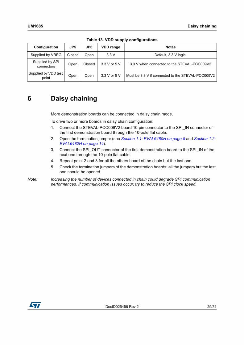
UM1685 Daisy chaining
31
6 Daisy chaining
More demonstration boards can be connected in daisy chain mode.
To drive two or more boards in daisy chain configuration:
1. Connect the STEVAL-PCC009V2 board 10-pin connector to the SPI_IN connector of the first demonstration board through the 10-pole flat cable.
2. Open the termination jumper (see Section 1.1: EVAL6480H on page 5 and Section 1.2: EVAL6482H on page 14).
3. Connect the SPI_OUT connector of the first demonstration board to the SPI_IN of the next one through the 10-pole flat cable.
4. Repeat point 2 and 3 for all the others board of the chain but the last one.
5. Check the termination jumpers of the demonstration boards: all the jumpers but the last one should be opened.
Note: Increasing the number of devices connected in chain could degrade SPI communication performances. If communication issues occur, try to reduce the SPI clock speed.
Table 13. VDD supply configurations
Configuration JP5 JP6 VDD range Notes
Supplied by VREG Closed Open 3.3 V Default, 3.3 V logic.
Supplied by SPI connectors
Open Closed 3.3 V or 5 V 3.3 V when connected to the STEVAL-PCC009V2
Supplied by VDD test point
Open Open 3.3 V or 5 V Must be 3.3 V if connected to the STEVAL-PCC009V2

Revision history UM1685
30/31 DocID025458 Rev 2
7 Revision history
Table 14. Document revision history
Date Revision Changes
28-Nov-2013 1 Initial release.
08-Apr-2015 2
Updated Section : Introduction on page 1 (replaced “cSPIN™” and “cSPIN™ family” by “L648x”).
Updated Figure 4: EVAL6480H - layout (top layer) on page 12 to Figure 7: EVAL6480H - layout (bottom layer ) on page 13 (converted to greyscale).
Removed Figure 11. EVAL6482H - layout (silkscreen) from page 20.
Updated title of the AN4354 (replaced “cSPIN™ family” by “L648x devices:”) in Section 3: Device configuration on page 24.
Minor modifications throughout document.

DocID025458 Rev 2 31/31
UM1685
31
IMPORTANT NOTICE – PLEASE READ CAREFULLY
STMicroelectronics NV and its subsidiaries (“ST”) reserve the right to make changes, corrections, enhancements, modifications, and improvements to ST products and/or to this document at any time without notice. Purchasers should obtain the latest relevant information on ST products before placing orders. ST products are sold pursuant to ST’s terms and conditions of sale in place at the time of order acknowledgement.
Purchasers are solely responsible for the choice, selection, and use of ST products and ST assumes no liability for application assistance or the design of Purchasers’ products.
No license, express or implied, to any intellectual property right is granted by ST herein.
Resale of ST products with provisions different from the information set forth herein shall void any warranty granted by ST for such product.
ST and the ST logo are trademarks of ST. All other product or service names are the property of their respective owners.
Information in this document supersedes and replaces information previously supplied in any prior versions of this document.
© 2015 STMicroelectronics – All rights reserved