EUV lithography: technology for the semi conductor ...
4
EUV lithography: technology for the semi- conductor industry in 2010 H. Enktsch and J. Trenkler Carl Zeiss SMT AG, Oberkochen, Germany I n 1965, Moore described the progress in the development of semiconductor devices by a sentence that is now commonly known as Moore’s Law: “the number of transistors on a comput- er chip doubles every two years”. Moore’s Law is not only a description of the evolution until 1965 but rather has served as a roadmap for both the chip manufacturers and the suppliers of chip production tools since then. Lithography is the only manufacturing method ensuring both sufficient quality and high throughput of the chip production. The principle of lithography is similar to that of a sfide projector as illustrated in Fig. 1. Light from a source passes through a con- denser optics (illumination system) that ensured the homogenous illumination of a slide (mask) containing e.g. a black and white pattern of the structure to be printed. Another set of lenses pro- jects the slide onto the screen (photo-resist coated wafer) thereby performing a certain demagnification. By means of wet chemical processes, the illuminated areas of the resist are removed (if a “positive resist”is utilized), followed by etching or coating steps of the then uncovered parts. To produce a computer chip, numer- ous repetitions of the above cycle with different patterns are required. All patterns have to be accurately superimposed on top of each other demanding a positioning accuracy of the mask and the wafer better than the dimension of the pattern on the mask and on the wafer, respectively. Although the semiconductor lithography has basically existed since the sixties, the basic equations governing the imaging process have been known for about a century. They have been found by Ernst Abbe in the late 1860s while he was a professor Fig. 1: A lithography tool works similarly to a slide projector. A homogenously illuminated pattern (slide) is projected onto a resist-coated wafer (screen). (“Privatdozent”) for physics at the University of Jena. Nowadays, Abbe’s equation reads as: The resolution of any optical tool is given by RES = k1λ /NA, where RES is the half pitch, Xthe wavelength of the utilized radi- ation, NA the numerical aperture given by n sin α , n and a being the refractive index of the medium and the opening angle of the bunch of rays in the image point and k1is a complex process fac- tor. The other fundamental quantity is the depth of focus (DOF) described by DOF = λ/ NA2. The DOF basically defines the process window. The larger the DOF, the larger the process window of the machine. Thus, if smaller structures have to be produced by the litho- graphic process, one can either reduce k1, reduce the wavelength of the utilized light or increase the numerical aperture. All three approaches have been extensively used during the last two decades as illustrated by Fig. 2. It (implicitly) shows how the combination of a change of k1, a change of X, and a strong change of the NA resulted in a reduction of the smallest achievable structure by a factor of 10. By using the immersion technique (between the last lens of the projection optics and the resist, aliquid medium with high refractive index is introduced) a NA of well above 1 may be possible. It is expected that with immersion tools operating for instance at 193nm, a res- olution of 50 nm and below can be achieved. Although a change in X from 365nm to 157nm does not seem to be too dramatic at first glance, the consequences for the choice of materials for'the optical elements are severe: DUV and VUV light will be completely absorbed in optical glass. Thus, the material of the lens elements had to be changed from glass via quartz to CaF2. In Tab. 1, the transmission of a single lens element coated with anti-reflective coatings is shown. Assuming that a full optical column (illumination and projec- tion system together) consists of up to 60 lens elements, the total transmission of a lithography tool drops from about 60% to 20%, significantly reducing the throughput (i.e. the illu- minated wafer per hour) of the whole tool. Without an appropriate anti-reflective coating on every surface, the losses due to reflection would further reduce the transmission to an unacceptable level. europhysics news september/ october 2004 Article available at http://www.europhvsicsnews.org or http://dx.doi.ora/10.1051/epn:2004503 149 features FEATURES Fig. 2:The "realization"of Moore's Law.
Transcript of EUV lithography: technology for the semi conductor ...
EUV lithography:technology for the semiconductor industry in 2010H. Enktsch and J. TrenklerCarl Zeiss SMT AG, Oberkochen, Germany
In 1965, Moore described the progress in the development of semiconductor devices by a sentence that is now commonly
known as Moore’s Law: “the number of transistors on a computer chip doubles every two years”. Moore’s Law is not only a description of the evolution until 1965 but rather has served as a roadmap for both the chip manufacturers and the suppliers of chip production tools since then.
Lithography is the only manufacturing method ensuring both sufficient quality and high throughput of the chip production. The principle of lithography is similar to that of a sfide projector as illustrated in Fig. 1. Light from a source passes through a condenser optics (illumination system) that ensured the homogenous illumination of a slide (mask) containing e.g. a black and white pattern of the structure to be printed. Another set of lenses projects the slide onto the screen (photo-resist coated wafer) thereby performing a certain demagnification. By means of wet chemical processes, the illuminated areas of the resist are removed (if a “positive resist” is utilized), followed by etching or coating steps of the then uncovered parts. To produce a computer chip, numerous repetitions of the above cycle with different patterns are required. All patterns have to be accurately superimposed on top of each other demanding a positioning accuracy of the mask and the wafer better than the dimension of the pattern on the mask and on the wafer, respectively.
Although the semiconductor lithography has basically existed since the sixties, the basic equations governing the imaging process have been known for about a century. They have been found by Ernst Abbe in the late 1860s while he was a professor
Fig. 1: A lithography tool works similarly to a slide projector. A homogenously illuminated pattern (slide) is projected onto a resist-coated wafer (screen).
(“Privatdozent”) for physics at the University of Jena. Nowadays, Abbe’s equation reads as:The resolution of any optical tool is given by
RES = k1 λ /NA,
where RES is the half pitch, X the wavelength of the utilized radiation, NA the numerical aperture given by n sinα, n and a being the refractive index of the medium and the opening angle of the bunch of rays in the image point and k1 is a complex process factor.
The other fundamental quantity is the depth of focus (DOF) described by
DOF = λ/ NA2.
The DOF basically defines the process window. The larger the DOF, the larger the process window of the machine.
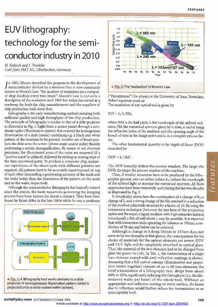
Thus, if smaller structures have to be produced by the lithographic process, one can either reduce k1, reduce the wavelength of the utilized light or increase the numerical aperture. All three approaches have been extensively used during the last two decades as illustrated by Fig. 2.
It (implicitly) shows how the combination of a change of k1, a change of X, and a strong change of the NA resulted in a reduction of the smallest achievable structure by a factor of 10. By using the immersion technique (between the last lens of the projection optics and the resist, a liquid medium with high refractive index is introduced) a NA of well above 1 may be possible. It is expected that with immersion tools operating for instance at 193nm, a resolution of 50 nm and below can be achieved.
Although a change in X from 365nm to 157nm does not seem to be too dramatic at first glance, the consequences for the choice of materials for'the optical elements are severe: DUV and VUV light will be completely absorbed in optical glass. Thus, the material of the lens elements had to be changed from glass via quartz to CaF2. In Tab. 1, the transmission of a single lens element coated with anti-reflective coatings is shown. Assuming that a full optical column (illumination and projection system together) consists of up to 60 lens elements, the total transmission of a lithography tool drops from about 60% to 20%, significantly reducing the throughput (i.e. the illuminated wafer per hour) of the whole tool. Without an appropriate anti-reflective coating on every surface, the losses due to reflection would further reduce the transmission to an unacceptable level.
europhysics news september/ october 2004Article available at http://www.europhvsicsnews.org or http://dx.doi.ora/10.1051/epn:2004503
149
feat
ures
FEATURES
Fig. 2:The "realization"of Moore's Law.
FEATURES
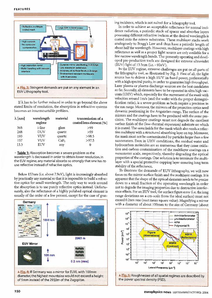
Fig. 3: Stringent demands are put on any element in an EUV Lithography tool.
If X has to be further reduced in order to go beyond the above stated limits of resolution, the absorption in refractive systems becomes an insurmountable problem.
λ [. m] wavelengthregime
material transmission of a coated lens element [%]
365 i-line glass >99248 DUV quartz >99193 VUV quartz >98.5157 VUV CaF2 >97.513.5 EUV any 0
- Table 1: Absorption becomes a severe problem as the wavelength is decreased in order to obtain lower resolution. In the EUV regime, any material absorbs so strongly that one has to use reflective instead of refractive optics.
Below 157nm (i.e. above 7.9eV), light is increasingly absorbed by practically any material so that it is impossible to build a refractive optics for small wavelength. The only way to work around the absorption is to use purely reflective optics instead. Unfortunately, also the reflectance of a highly polished optical element is usually of the order of a few percent, except for the case of graz
Fig.4: If Germany was a mirror for EUVL with 100mm diameter,the highest mountains would not exceed a height of 5mm instead of the 295.0m of the Zugspitze.
ing incidence, which is not suited for a lithography tool.In order to achieve an acceptable reflectance for normal inci
dence radiation, a periodic stack of spacer and absorber layers possessing different refractive indices at the desired wavelength is coated onto the mirror substrates. These multilayer stacks work analogously to Bragg’s Law and thus have a periodic length of about half the wavelength. However, multilayer coatings with high reflectance as well as a proper light source are only available for a few narrow wavelength bands. The presently operating and developed pre-production tools are designed for extreme ultraviolet (EUV) light of 13.5nm (i.e. ~92eV).
In the EUV regime, extreme challenges are put on all parts of the lithography tool, as illustrated by Fig. 3. First of all, the light source has to deliver a high EUV in-band power, preferentially with a high spectral purity, in order to guarantee high throughput. Laser plasma or plasma discharge sources are the best candidates so far. Secondly, all elements have to be operated in ultra high vacuum (UHV) which, especially for the movement of the mask with velocities around lm/s (and the wafer with the proper demagnification ratio), is a severe problem as both require a precision in the nm range. Moreover, the mirrors of the projection optics need dynamic positioning in the Angström-range. The surface of the mirrors and the coatings have to be produced with the same precision. The multilayer coatings must not degrade the excellent surface finish of the (low-thermal expansion) substrate on which it is coated. The same holds for the mask which also needs a reflective multilayer with a structured absorbing layer on top. Moreover, the mask must not be contaminated by particles larger than a few nanometers. Even in UHV conditions, the residual water and hydrocarbon molecules are so numerous that they cause oxidation and carbon contamination of the multilayer coatings on a nanometer scale, respectively, thereby degrading the optical properties of the coatings. One solution is to terminate the multilayer with a special protective capping layer ensuring long term stability of the reflectance.
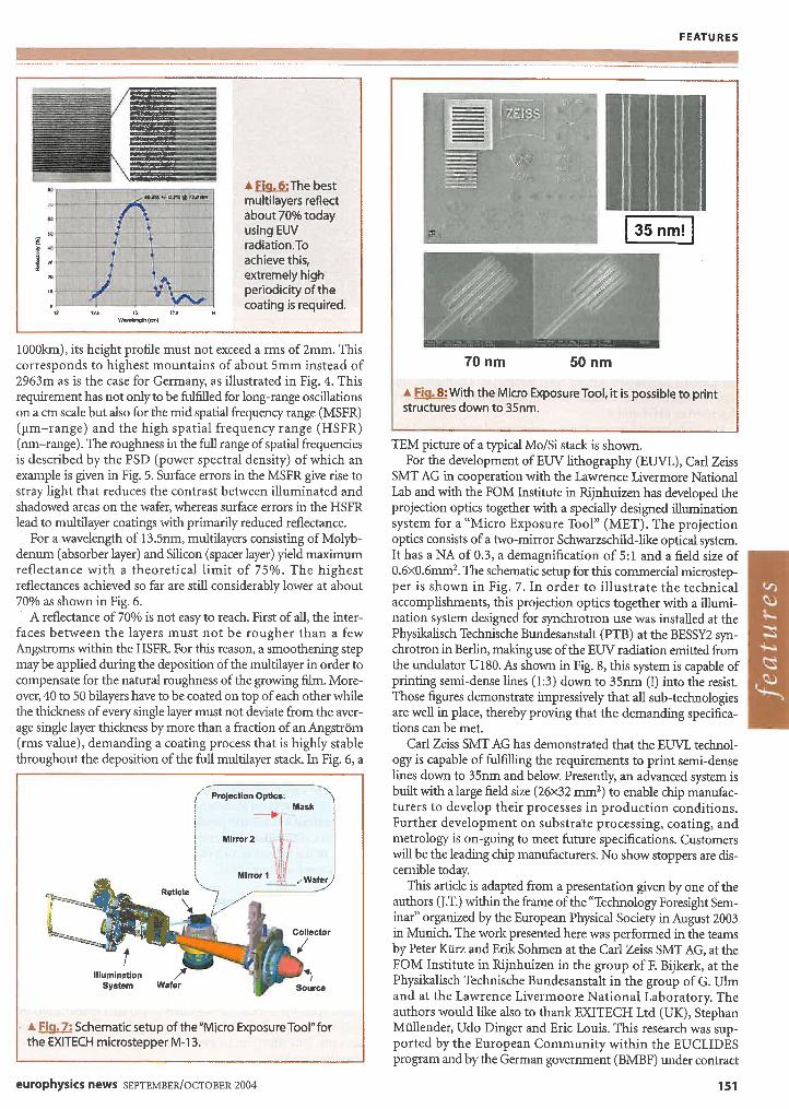
To illustrate the demands of EUV lithography, we will now focus on the mirror surface finish and the multilayer coatings. It is apparent that the shape of the optical elements needs to be precise down to a small fraction of the operating wavelength in order not to degrade the imaging properties due to destructive interference effects. For an EUV tool, the surface figure error (i.e. the long range deviations on a cm-scale from the ideal surface) must not exceed 0.2nm rms (root mean square value). Magnifying a mirror with a diameter of about 100mm to the size of Germany (about
Fig.5: Roughnesses of all spatial regimes are described by the power spectral density (PSD).
150 europhysics news september/ october 2004
FEATURES
Fig. 6: The best multilayers reflect about 70% today using EUV radiation.To achieve this, extremely high periodicity of the coating is required.
1000km), its height profile must not exceed a rms of 2mm. This corresponds to highest mountains of about 5mm instead of 2963m as is the case for Germany, as illustrated in Fig. 4. This requirement has not only to be fulfilled for long-range oscillations on a cm scale but also for the mid spatial frequency range (MSFR) (pm-range) and the high spatial frequency range (HSFR) (nm-range). The roughness in the fiali range of spatial frequencies is described by the PSD (power spectral density) of which an example is given in Fig. 5. Surface errors in the MSFR give rise to stray light that reduces the contrast between illuminated and shadowed areas on the wafer, whereas surface errors in the HSFR lead to multilayer coatings with primarily reduced reflectance.
For a wavelength of 13.5nm, multilayers consisting of Molybdenum (absorber layer) and Silicon (spacer layer) yield maximum reflectance with a theoretical limit of 75%. The highest reflectances achieved so far are still considerably lower at about 70% as shown in Fig. 6.
A reflectance of 70% is not easy to reach. First of all, the interfaces between the layers must not be rougher than a few Angstroms within the HSFR. For this reason, a smoothening step may be applied during the deposition of the multilayer in order to compensate for the natural roughness of the growing film. Moreover, 40 to 50 bilayers have to be coated on top of each other while the thickness of every single layer must not deviate from the average single layer thickness by more than a fraction of an Angstrom (rms value), demanding a coating process that is highly stable throughout the deposition of the fiali multilayer stack. In Fig. 6, a
Fig. 7: Schematic setup of the "Micro Exposure Tool"for the EXITECH microstepper M-13.
Fig. 8: With the Micro Exposure Tool, it is possible to print structures down to 35nm.
TEM picture of a typical Mo/Si stack is shown.For the development of EUV lithography (EUVL), Carl Zeiss
SMT AG in cooperation with the Lawrence Livermore National Lab and with the FOM Institute in Rijnhuizen has developed the projection optics together with a specially designed illumination system for a “Micro Exposure Tool” (MET). The projection optics consists of a two-mirror Schwarzschild-like optical system. It has a NA of 0.3, a demagnification of 5:1 and a field size of 0.6x0.6mm2. The schematic setup for this commercial microstepper is shown in Fig. 7. In order to illustrate the technical accomplishments, this projection optics together with a illumination system designed for synchrotron use was installed at the Physikalisch Technische Bundesanstalt (PTB) at the BESSY2 synchrotron in Berlin, making use of the EUV radiation emitted from the undulator U180. As shown in Fig. 8, this system is capable of printing semi-dense lines (1:3) down to 35nm (!) into the resist. Those figures demonstrate impressively that all sub-technologies are well in place, thereby proving that the demanding specifications can be met.
Carl Zeiss SMT AG has demonstrated that the EUVL technology is capable of fulfilling the requirements to print semi-dense lines down to 35nm and below. Presently, an advanced system is built with a large field size (26x32 mm2) to enable chip manufacturers to develop their processes in production conditions. Further development on substrate processing, coating, and metrology is on-going to meet future specifications. Customers will be the leading chip manufacturers. No show stoppers are discernible today.
This article is adapted from a presentation given by one of the authors (J.T.) within the frame of the “Technology Foresight Seminar” organized by the European Physical Society in August 2003 in Munich. The work presented here was performed in the teams by Peter Kürz and Erik Sohmen at the Carl Zeiss SMT AG, at the FOM Institute in Rijnhuizen in the group of F. Bijkerk, at the Physikalisch Technische Bundesanstalt in the group of G. Ulm and at the Lawrence Livermoore National Laboratory. The authors would like also to thank EXITECH Ltd (UK), Stephan Müllender, Udo Dinger and Eric Louis. This research was supported by the European Community within the EUCLID ES program and by the German government (BMBF) under contract
europhysics news september/october 2004 151
feat
ures
FEATURES
Ion tracks - a new route to nanotechnologyAlois Weidinger, Hahn-Meitner Institute Berlin, Berlin, Germany
Jon tracks are created when high-energetic heavy ions with energy of about 1 MeV/nucleon (e.g. 140 MeV Xe ions) pass through matter. The extremely high local energy deposition along the path leads to a material transformation within a narrow cylinder of about 10 nm width. Unlike in the more conventional lithographic techniques based on ion or electron beam irradiation, a single heavy ion suffices to transform the material. Thus, problems like straggling or diffusively broadened features do not occur. Ion beams with the required properties are available e.g. at the national accelerator centres HMI Berlin, GSI Darmstadt and GANIL Caen. Some recent developments of this field are described in Ref. 1 and 2.Ion tracks have a long tradition in science and technology. They
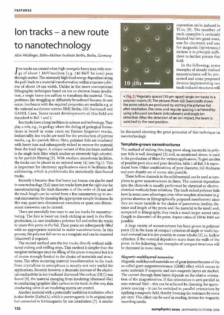
play a role, e.g., in geology where the dating of geological formations is based in some cases on fission fragment tracks. Industrially, ion tracks are used for the production of porous media, e.g. for particle filters. Here, polymer foils are irradiated with heavy ions and subsequently etched to remove the material from the track region. A unique variant of this ion beam method is the single-hole filter which reaches an extremely high selectivity for particle filtering [3]. With modern microbeam facilities, the tracks can be placed in an ordered array [4] (see Fig.l). This is important for electronic applications since it facilitates the addressing, which is problematic for statistically distributed tracks.
Recently it became clear that heavy ion beams can also be used in nanotechnology [5,6] since ion tracks have just the right size for nanostructuring: the track diameter is of the order of 10 run and the track length can be varied from a few nanometers up to several micrometers by choosing the appropriate sample thickness. In this way, quasi zero-dimensional nanodots or quasi one-dimensional nanowires can be created.
There are essentially two ways to use ion tracks for nanostructuring. The first is based on track etching as used in the filter production, i.e. one irradiates a polymer foil and etches the tracks to create thin pores in the foil. These pores are subsequently filled with an appropriate material to make nanostructures. In this process, the polymer foil serves as a template and can be removed (dissolved) if required.
The second method uses the ion tracks directly without additional etching and refilling steps. This method is simpler than the template technique since no filling of the pores is required but it is of course strongly limited in the choice of materials and structures. The often occurring material transformation in the track from crystalline to amorphous is mostly not very useful for applications. Recently however, a dramatic increase of the electrical conductivity in ion irradiated diamond-like carbon (DLC) was found [6], the material changing from insulating (diamond-like) to conducting (graphite-like) carbon in the track. In this way, thin conducting wires in an insulating matrix are created.
Another material with a potentially usefid ion irradiation effect is zinc-ferrite (ZnFe2O4) which is paramagnetic in its original state but converted to ferrimagnetic by ion irradiation [7]. A similar
Ion tracks are created when high-energetic heavy ions with energy of about 1 MeV/nucleon (e.g. 140 MeV Xe ions) pass
through matter. The extremely high local energy deposition along the path leads to a material transformation within a narrow cylinder of about 10 nm width. Unlike in the more conventional lithographic techniques based on ion or electron beam irradiation, a single heavy ion suffices to transform the material. Thus, problems like straggling or diffusively broadened features do not occur. Ion beams with the required properties are available e.g. at the national accelerator centres HMI Berlin, GSI Darmstadt and GANIL Caen. Some recent developments of this field are described in Ref. 1 and 2.
Ion tracks have a long tradition in science and technology. They play a role, e.g., in geology where the dating of geological formations is based in some cases on fission fragment tracks. Industrially, ion tracks are used for the production of porous media, e.g. for particle filters. Here, polymer foils are irradiated with heavy ions and subsequently etched to remove the material from the track region. A unique variant of this ion beam method is the single-hole filter which reaches an extremely high selectivity for particle filtering [3]. With modern microbeam facilities, the tracks can be placed in an ordered array [4] (see Fig.l). This is important for electronic applications since it facilitates the addressing, which is problematic for statistically distributed tracks.
Recently it became clear that heavy ion beams can also be used in nanotechnology [5,6] since ion tracks have just the right size for nanostructuring: the track diameter is of the order of 10 run and the track length can be varied from a few nanometers up to several micrometers by choosing the appropriate sample thickness. In this way, quasi zero-dimensional nanodots or quasi one-dimensional nanowires can be created.
There are essentially two ways to use ion tracks for nanostructuring. The first is based on track etching as used in the filter production, i.e. one irradiates a polymer foil and etches the tracks to create thin pores in the foil. These pores are subsequently filled with an appropriate material to make nanostructures. In this process, the polymer foil serves as a template and can be removed (dissolved) if required.
The second method uses the ion tracks directly without additional etching and refilling steps. This method is simpler than the template technique since no filling of the pores is required but it is of course strongly limited in the choice of materials and structures. The often occurring material transformation in the track from crystalline to amorphous is mostly not very useful for applications. Recently however, a dramatic increase of the electrical conductivity in ion irradiated diamond-like carbon (DLC) was found [6], the material changing from insulating (diamond-like) to conducting (graphite-like) carbon in the track. In this way, thin conducting wires in an insulating matrix are created.
Another material with a potentially usefid ion irradiation effect is zinc-ferrite (ZnFe2O4) which is paramagnetic in its original state but converted to ferrimagnetic by ion irradiation [7]. A similar
be discussed showing the great potential of this technique in nanotechnology.
Template-grown nanostructuresThe method of etching thin long pores along ion tracks in polymer foils is well developed [2] and, as mentioned above, is used in the production of filters for various applications. To give an idea of possible pore sizes and pore densities, table 1 of Ref. 2 is reproduced here. Other combinations of pore diameter, foil thickness and pore density are of course also possible.
These hollow channels in the solid material can be used as templates to grow nanostructures in them. The material deposition into the channels is usually performed by chemical or electrochemical methods from solutions. The track etched polymer foils have in some cases advantages over other template structures (e.g. porous alumina or lithographically prepared membranes) since they are more variable in the choice of parameters (radius, distance and length of the pores and the material to be used) and, compared to lithography, they reach a much larger aspect ratio (length to diameter) of the pores. Aspect ratios of 100 to 1000 are possible.
A large variety of nanostructures has been grown in polymer pores [5] in the form of compact cylinders of single or multi-layered material but it is also possible to create tubules [2], i.e. hollow cylinders, if the material deposition starts from the walls of the pores. In the following, two examples of compact structures will be discussed in more detail.
Magnetic multilayered nanowiresMagnetic multilayered materials are of great interest because of the so-called giant magnetoresistance (GMR) effect which occurs in some materials if magnetic and non-magnetic layers are stacked. The current through these layers depends on the relative orientation of the magnetisation. If this orientation is anti-parallel in zero external field - this can be achieved by choosing the appropriate spacing - it can be switched to parallel orientation by applying a magnetic field, thereby lowering the resistance by some per cent. This effect can be used in reading devices for magnetic recording media.
conversion can be induced in YC02 [8]. The number of such examples is certainly limited but two good ones, one for electronic and one for magnetic (spintronic) devices is in principle sufficient to further pursue this field.
In the following, some examples of already realized nanostructures will be presented and some proposed devices implementing ion track-induced structures will
F ig .1 : Regularly spaced (10 pm apart) single ion tracks in a I polymer matrix [4].The picture (from GSI Darmstadt) shows j
the pores which are produced by etching the polymer foil after irradiation.The close and regular spacing is achieved by using a focused ion beam (microbeam) and single ion detection. After the detection of an ion impact, the beam is switched to the next position.
152 europhysics news september/ october 2004