EUV Lithography – A Historical Perspective Hiroo Kinoshita...
65
EUV Lithography Introduction, Status and Challenges Vivek Bakshi, Ph.D. EUV Litho Inc. 10202 Womack Road, Austin, TX 78748 USA www.euvlitho.com [email protected]
Transcript of EUV Lithography – A Historical Perspective Hiroo Kinoshita...
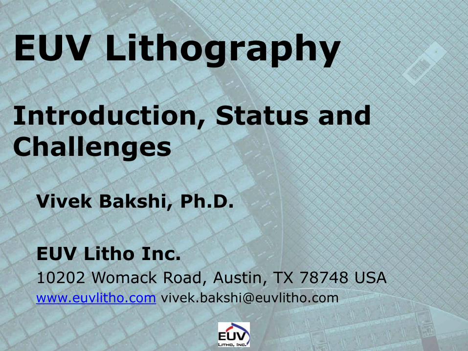
EUV Lithography Introduction, Status and Challenges Vivek Bakshi, Ph.D.
EUV Litho Inc.
10202 Womack Road, Austin, TX 78748 USA
www.euvlitho.com [email protected]
Outline
• Introduction to EUV Lithography
• Technical Status and Challenges
• Summary
Outline
• Introduction to EUV Lithography
• Technical Status and Challenges
• Summary
4
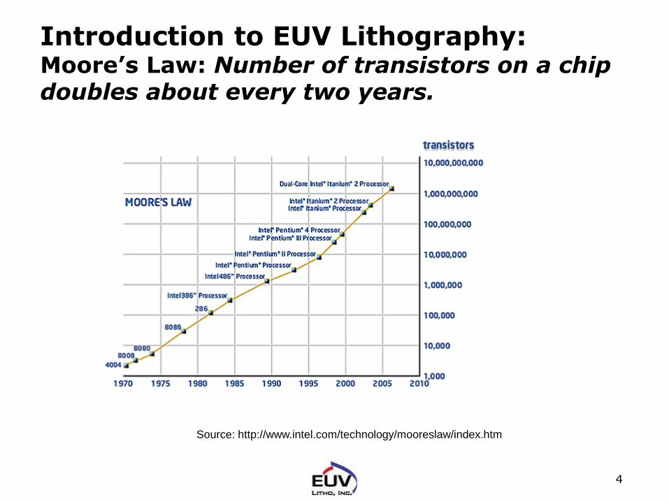
Introduction to EUV Lithography: Moore’s Law: Number of transistors on a chip doubles about every two years.
Source: http://www.intel.com/technology/mooreslaw/index.htm

Introduction to EUV Lithography: EUVL is the leading Lithography Technology for 22 nm node and Beyond (2009 ITRS)
www.itrs.net
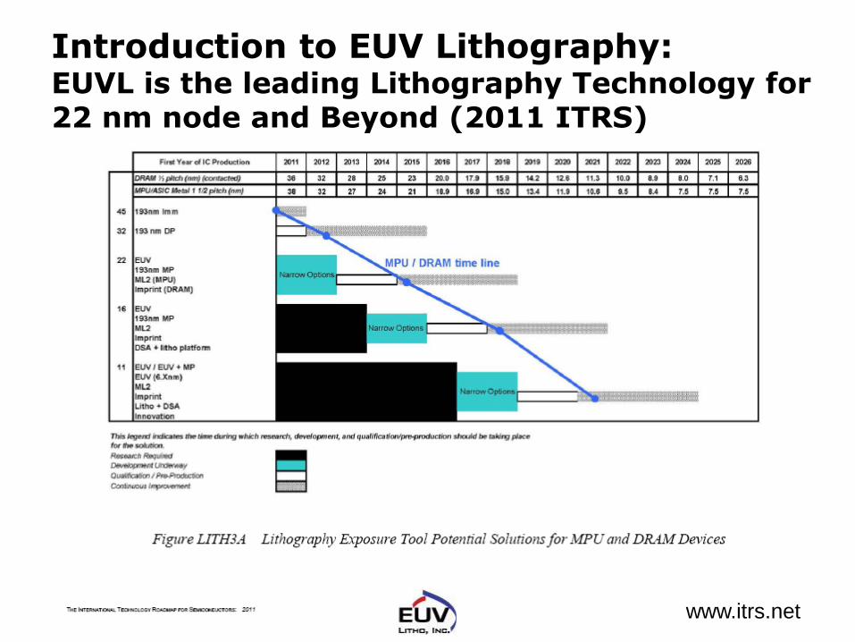
Introduction to EUV Lithography: EUVL is the leading Lithography Technology for 22 nm node and Beyond (2011 ITRS)
www.itrs.net
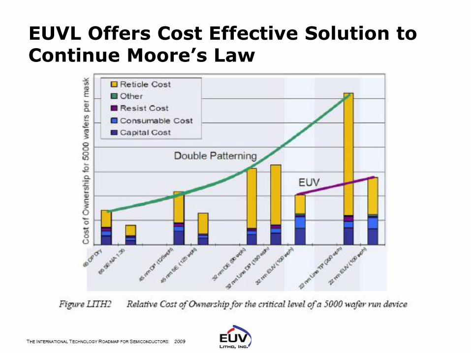
EUVL Offers Cost Effective Solution to Continue Moore’s Law
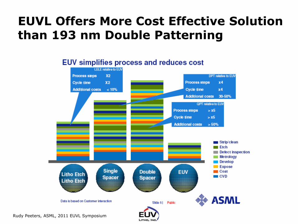
EUVL Offers More Cost Effective Solution than 193 nm Double Patterning
Rudy Peeters, ASML, 2011 EUVL Symposium
10
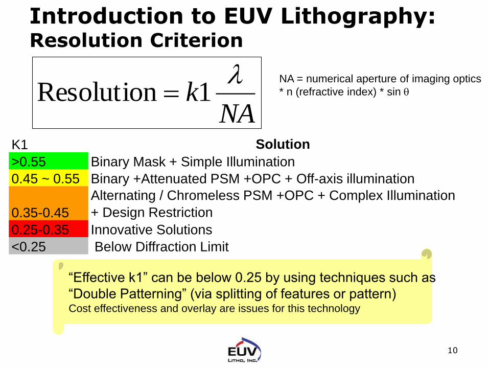
Introduction to EUV Lithography: Resolution Criterion
NAk
1Resolution
NA = numerical aperture of imaging optics
* n (refractive index) * sin q
“Effective k1” can be below 0.25 by using techniques such as
“Double Patterning” (via splitting of features or pattern) Cost effectiveness and overlay are issues for this technology
K1 Solution
>0.55 Binary Mask + Simple Illumination
0.45 ~ 0.55 Binary +Attenuated PSM +OPC + Off-axis illumination
0.35-0.45
Alternating / Chromeless PSM +OPC + Complex Illumination
+ Design Restriction
0.25-0.35 Innovative Solutions
<0.25 Below Diffraction Limit
11
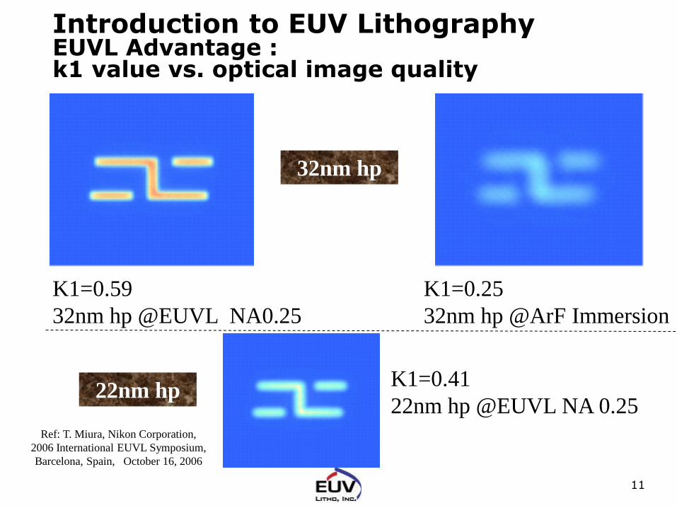
Introduction to EUV Lithography EUVL Advantage : k1 value vs. optical image quality
K1=0.59
32nm hp @EUVL NA0.25
K1=0.25
32nm hp @ArF Immersion
K1=0.41
22nm hp @EUVL NA 0.25
32nm hp
22nm hp
Ref: T. Miura, Nikon Corporation,
2006 International EUVL Symposium,
Barcelona, Spain, October 16, 2006

Wavelength Reduction has been a key Driver of Moore’s Law
Lithography gets Extreme, Christian Wagener and Noreen Harned, Nature Photonics, Vol. 4, pp. 24-26, January 2010
Factor of 1.5
Factor of 1.3
Factor of 14
13
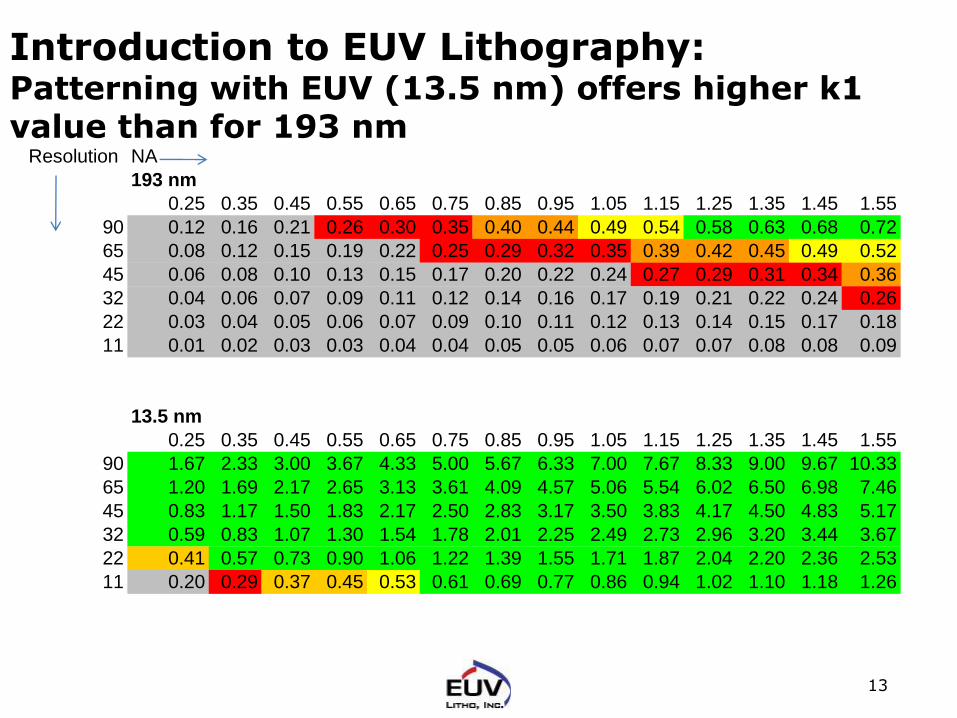
Introduction to EUV Lithography: Patterning with EUV (13.5 nm) offers higher k1 value than for 193 nm
Resolution NA
193 nm
0.25 0.35 0.45 0.55 0.65 0.75 0.85 0.95 1.05 1.15 1.25 1.35 1.45 1.55
90 0.12 0.16 0.21 0.26 0.30 0.35 0.40 0.44 0.49 0.54 0.58 0.63 0.68 0.72
65 0.08 0.12 0.15 0.19 0.22 0.25 0.29 0.32 0.35 0.39 0.42 0.45 0.49 0.52
45 0.06 0.08 0.10 0.13 0.15 0.17 0.20 0.22 0.24 0.27 0.29 0.31 0.34 0.36
32 0.04 0.06 0.07 0.09 0.11 0.12 0.14 0.16 0.17 0.19 0.21 0.22 0.24 0.26
22 0.03 0.04 0.05 0.06 0.07 0.09 0.10 0.11 0.12 0.13 0.14 0.15 0.17 0.18
11 0.01 0.02 0.03 0.03 0.04 0.04 0.05 0.05 0.06 0.07 0.07 0.08 0.08 0.09
13.5 nm
0.25 0.35 0.45 0.55 0.65 0.75 0.85 0.95 1.05 1.15 1.25 1.35 1.45 1.55
90 1.67 2.33 3.00 3.67 4.33 5.00 5.67 6.33 7.00 7.67 8.33 9.00 9.67 10.33
65 1.20 1.69 2.17 2.65 3.13 3.61 4.09 4.57 5.06 5.54 6.02 6.50 6.98 7.46
45 0.83 1.17 1.50 1.83 2.17 2.50 2.83 3.17 3.50 3.83 4.17 4.50 4.83 5.17
32 0.59 0.83 1.07 1.30 1.54 1.78 2.01 2.25 2.49 2.73 2.96 3.20 3.44 3.67
22 0.41 0.57 0.73 0.90 1.06 1.22 1.39 1.55 1.71 1.87 2.04 2.20 2.36 2.53
11 0.20 0.29 0.37 0.45 0.53 0.61 0.69 0.77 0.86 0.94 1.02 1.10 1.18 1.26
14
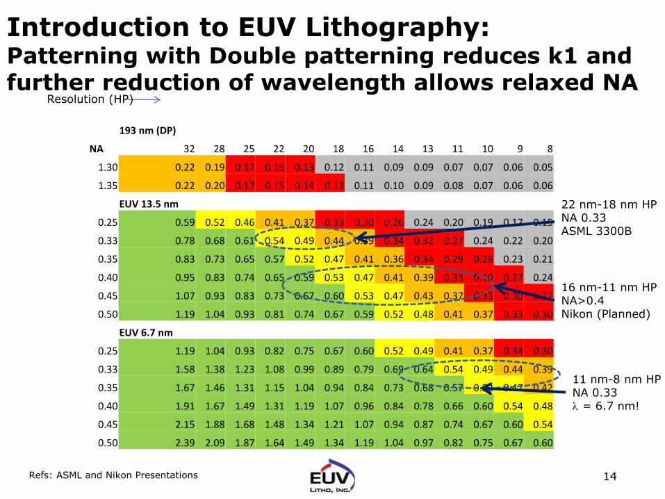
Introduction to EUV Lithography: Patterning with Double patterning reduces k1 and further reduction of wavelength allows relaxed NA
193 nm (DP)
NA 32 28 25 22 20 18 16 14 13 11 10 9 8
1.30 0.22 0.19 0.17 0.15 0.13 0.12 0.11 0.09 0.09 0.07 0.07 0.06 0.05
1.35 0.22 0.20 0.17 0.15 0.14 0.13 0.11 0.10 0.09 0.08 0.07 0.06 0.06
EUV 13.5 nm
0.25 0.59 0.52 0.46 0.41 0.37 0.33 0.30 0.26 0.24 0.20 0.19 0.17 0.15
0.33 0.78 0.68 0.61 0.54 0.49 0.44 0.39 0.34 0.32 0.27 0.24 0.22 0.20
0.35 0.83 0.73 0.65 0.57 0.52 0.47 0.41 0.36 0.34 0.29 0.26 0.23 0.21
0.40 0.95 0.83 0.74 0.65 0.59 0.53 0.47 0.41 0.39 0.33 0.30 0.27 0.24
0.45 1.07 0.93 0.83 0.73 0.67 0.60 0.53 0.47 0.43 0.37 0.33 0.30 0.27
0.50 1.19 1.04 0.93 0.81 0.74 0.67 0.59 0.52 0.48 0.41 0.37 0.33 0.30
EUV 6.7 nm
0.25 1.19 1.04 0.93 0.82 0.75 0.67 0.60 0.52 0.49 0.41 0.37 0.34 0.30
0.33 1.58 1.38 1.23 1.08 0.99 0.89 0.79 0.69 0.64 0.54 0.49 0.44 0.39
0.35 1.67 1.46 1.31 1.15 1.04 0.94 0.84 0.73 0.68 0.57 0.52 0.47 0.42
0.40 1.91 1.67 1.49 1.31 1.19 1.07 0.96 0.84 0.78 0.66 0.60 0.54 0.48
0.45 2.15 1.88 1.68 1.48 1.34 1.21 1.07 0.94 0.87 0.74 0.67 0.60 0.54
0.50 2.39 2.09 1.87 1.64 1.49 1.34 1.19 1.04 0.97 0.82 0.75 0.67 0.60
Resolution (HP)
16 nm-11 nm HP NA>0.4 Nikon (Planned)
22 nm-18 nm HP NA 0.33 ASML 3300B
11 nm-8 nm HP NA 0.33 = 6.7 nm!
Refs: ASML and Nikon Presentations

EUVL can extend to < 5 nm Resolution!

16
Introduction to EUV Lithography: Why 13. 5 nm? Si/Mo Multilayer mirrors (ML) offer a narrow band-pass
filter, centered at 13. 5 nm, with peak reflectivity ~ 70%
0.00E+00
1.00E-01
2.00E-01
3.00E-01
4.00E-01
5.00E-01
6.00E-01
7.00E-01
8.00E-01
0 5 10 15 20 25 30 35 40
Wavelength (nm)
Refl
ecti
vit
y (
%)
Ref: http://www.cxro.lbl.gov
Si/Mo ML Reflectivity 0.1- 40 nm range
Si/Mo ML Reflectivity Note narrowing of band pass After seven reflections
Multilayer Reflectivty
0
0.2
0.4
0.6
0.8
1
1.2
12 12.5 13 13.5 14 14.5 15
Wavelength
Refl
ecti
vit
y (
No
rmali
zed
)
ML Reflectivity
ML Reflectivity (7 mirrors)

12,0 12,5 13,0 13,5 14,0 14,5 15,0
Sp
ectr
al in
ten
sit
y [
arb
. u
nit
s]
Wavelength [nm]
Spectral distribution after Mo/Si multilayer mirror reflection
10 11 12 13 14 15 16 170
1x10⁷
2x10⁷
3x10⁷
4x10⁷
5x10⁷
6x10⁷
7x10⁷
Sp
ectr
al in
ten
sity [
arb
. u
nits]
Wavelength [nm]
Introduction to EUV Lithography: Why 13. 5 nm? ML reflects only wavelengths around 13.5 nm – converting Multi wavelength Xe spectra to narrow band. Filter function works well around 13.5 nm !
Data Source: XTREME´s DPP Xenon Source
17

EUVL scanner uses ML Mirrors (instead of lenses)
Lithography gets Extreme, Christian Wagener and Noreen Harned, Nature Photonics, Vol. 4, pp. 24-26, January 2010

19
EUVL is Optical Lithography with following key differences from current Lithography :
• EUVL uses plasma sources (radiating at 13.5 nm) instead of Excimer lasers (193 nm) for high volume manufacturing
• 13.5 nm light is readily absorbed therefore – EUVL scanners use reflective instead of
refractive optics • EUV Optics and Reticles are Reflective multilayer
mirrors
– Entire EUVL scanner is kept in a high vacuum
• EUVL is the patterning technology for 32 nm half pitch and below.
– Resolution = k1 X Wavelength/Numerical Aperture • k1= 0.4, NA =0.25 NA, resolution = 22 nm
• k1= 0.32, NA =0.45 NA, resolution = 10 nm

Outline
• Introduction to EUV Lithography
• Technical Status and Challenges
– Source
– Mask
– Optics
– Resist
– Scanner
• Summary

EUV SOURCE STATUS
EUVL Technology Status
21
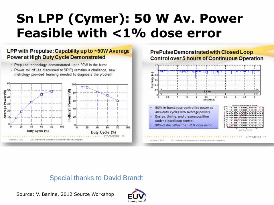
Sn LPP (Cymer): 50 W Av. Power Feasible with <1% dose error
Special thanks to David Brandt
Source: V. Banine, 2012 Source Workshop

Sn LPP (Cymer): LPP Scaling – Promise of Scaling to 250 W
LPP shows potential of scaling in low duty cycle experiments
Special thanks to David Brandt
Source: V. Banine, 2012 Source Workshop
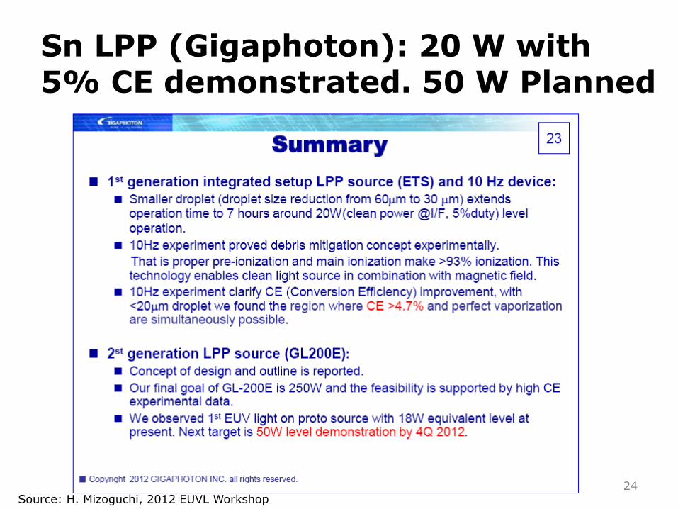
Sn LPP (Gigaphoton): 20 W with 5% CE demonstrated. 50 W Planned
24 Source: H. Mizoguchi, 2012 EUVL Workshop
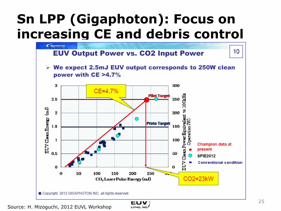
Sn LPP (Gigaphoton): Focus on increasing CE and debris control
25 Source: H. Mizoguchi, 2012 EUVL Workshop
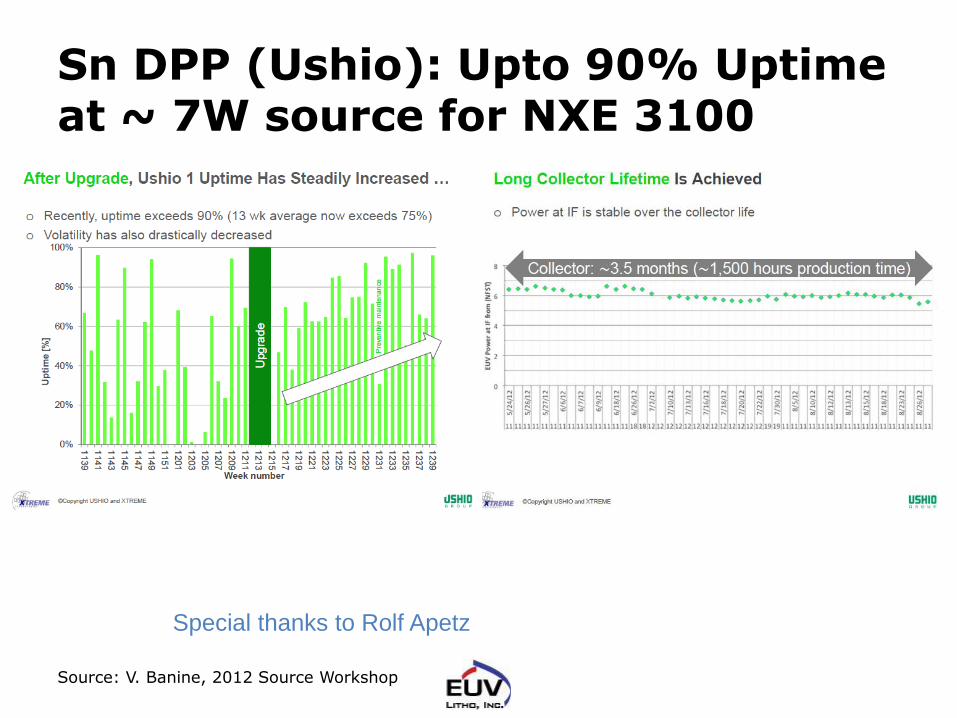
Sn DPP (Ushio): Upto 90% Uptime at ~ 7W source for NXE 3100
Special thanks to Rolf Apetz
Source: V. Banine, 2012 Source Workshop
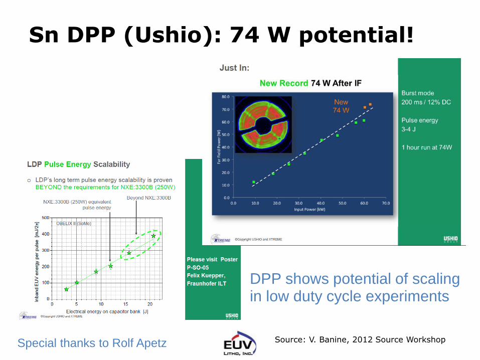
Sn DPP (Ushio): 74 W potential!
DPP shows potential of scaling in low duty cycle experiments
Special thanks to Rolf Apetz Source: V. Banine, 2012 Source Workshop
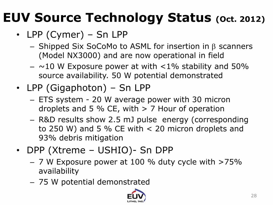
EUV Source Technology Status (Oct. 2012)
• LPP (Cymer) – Sn LPP
– Shipped Six SoCoMo to ASML for insertion in b scanners (Model NX3000) and are now operational in field
– ~10 W Exposure power at with <1% stability and 50% source availability. 50 W potential demonstrated
• LPP (Gigaphoton) – Sn LPP
– ETS system - 20 W average power with 30 micron droplets and 5 % CE, with > 7 Hour of operation
– R&D results show 2.5 mJ pulse energy (corresponding to 250 W) and 5 % CE with < 20 micron droplets and 93% debris mitigation
• DPP (Xtreme – USHIO)- Sn DPP
– 7 W Exposure power at 100 % duty cycle with >75% availability
– 75 W potential demonstrated
28
EUV target
25kW, 75kHz CO2 laser A
25kW, 75kHz CO2 laser B
500W, 150kHz thin disc laser
Configuration of 150kHz, 1kW EUV source
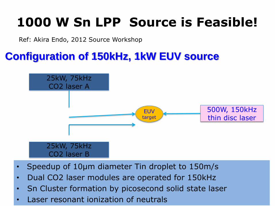
1000 W Sn LPP Source is Feasible!
• Speedup of 10μm diameter Tin droplet to 150m/s
• Dual CO2 laser modules are operated for 150kHz
• Sn Cluster formation by picosecond solid state laser
• Laser resonant ionization of neutrals
Ref: Akira Endo, 2012 Source Workshop

Challenges to Conventional Scaling of LPP
• CE increase viability at higher powers? (GPI @ SPIE 2012 reported 5%)
• Laser power scaling or multiplication
• Maintaining cold gas buffer for lifetime of the mirror at the 3-4x increase of power load
• Maintaining lifetime of collector at increased (3x-4x) Sn consumption (Is GI collector a viable idea in this case?
• Droplet generator scalability to higher frequencies?
Source: V. Banine, 2012 Source Workshop
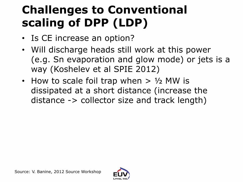
Challenges to Conventional scaling of DPP (LDP)
• Is CE increase an option?
• Will discharge heads still work at this power (e.g. Sn evaporation and glow mode) or jets is a way (Koshelev et al SPIE 2012)
• How to scale foil trap when > ½ MW is dissipated at a short distance (increase the distance -> collector size and track length)
Source: V. Banine, 2012 Source Workshop

List of Source R&D Topics
• How to increase and sustain CE increase
• Understanding Limits of CE and power
• New source configurations to enable power scaling of DPP and LPP
• Debris mitigation strategy for high power sources
• High brightness sources for metrology –development and understanding limits
• Ps, 500 W lasers for pre pulse for Sn LPP
• Development of 25-100 kW, pulsed CO2 laser modules
• Development of BEUV sources
• Development of non-plasma sources for HVM and BEUV 32
EUV MASK STATUS
EUVL Technology Status
33
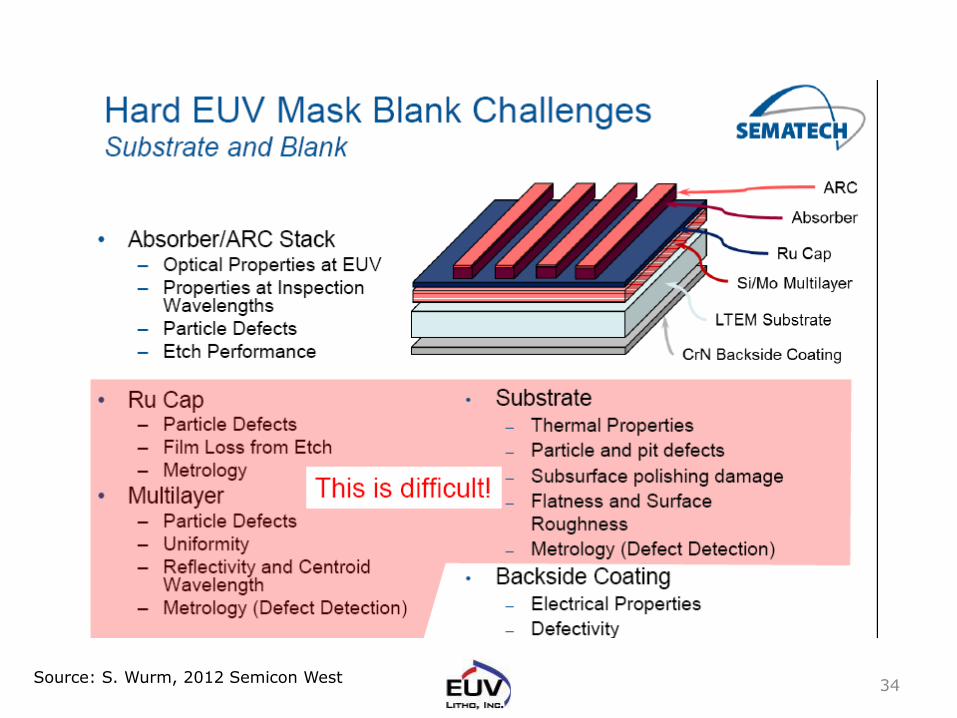
34 Source: S. Wurm, 2012 Semicon West
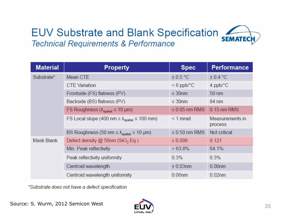
35 Source: S. Wurm, 2012 Semicon West

36 Source: S. Wurm, 2012 Semicon West

Actinic Mask Inspection Tools Needed
37

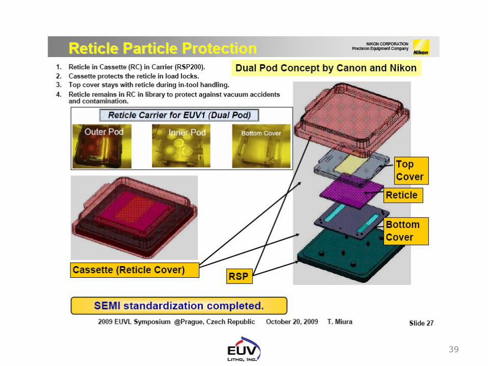
38
AIMS EUV Project Underway at Carl Zeiss: Tool to be Delivered by 2014 (Current Source brightness 8 W/mm2.sr, min needed 30 W /mm2.sr)
39
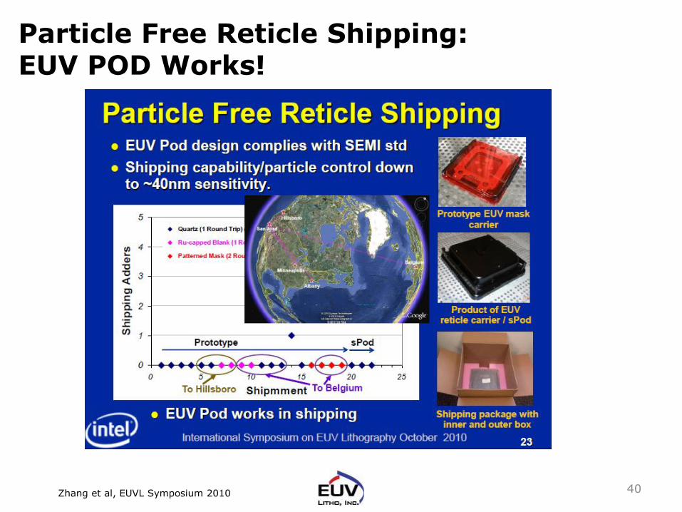
40 Zhang et al, EUVL Symposium 2010
Particle Free Reticle Shipping: EUV POD Works!
EUV OPTICS STATUS
EUVL Technology Status
41
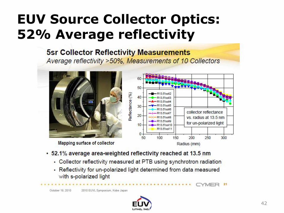
EUV Source Collector Optics: 52% Average reflectivity
42
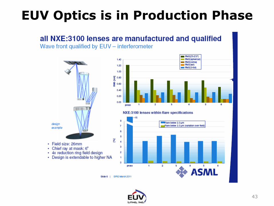
EUV Optics is in Production Phase
43
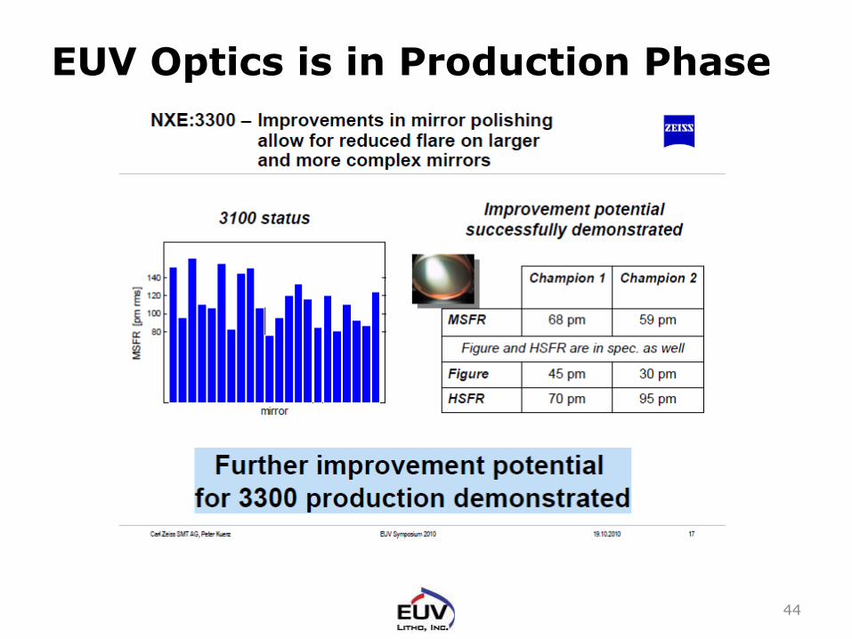
EUV Optics is in Production Phase
44
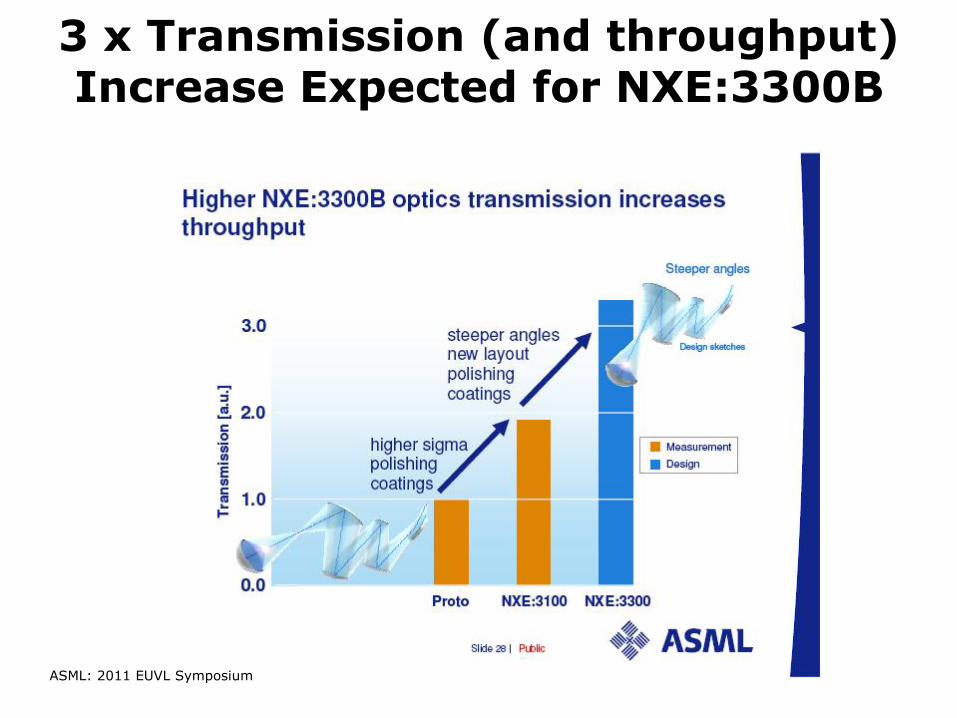
3 x Transmission (and throughput) Increase Expected for NXE:3300B
ASML: 2011 EUVL Symposium
46
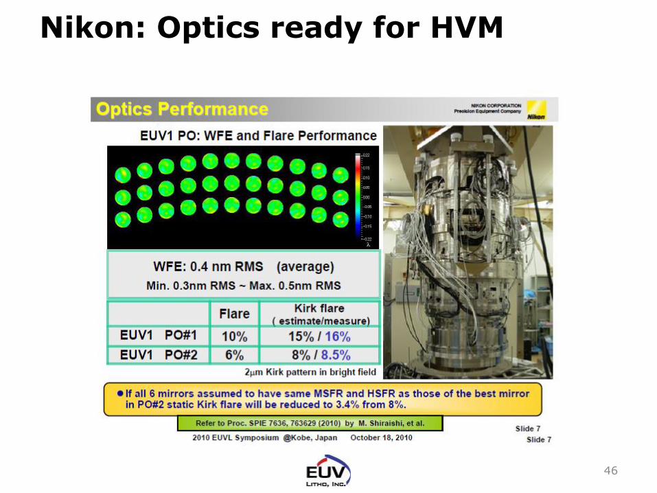
Nikon: Optics ready for HVM

Nikon: Optics ready for HVM
47
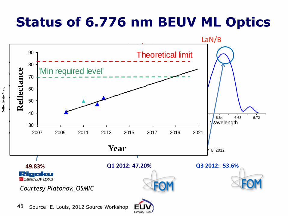
48
49.83%
La/B4C
Measured at New Subaru, 2011
Courtesy Platonov, OSMIC
Status of 6.776 nm BEUV ML Optics
Q1 2012: 47.20%
LaN/B4C
Measured at PTB, 2012
6.56 6.60 6.64 6.68 6.720.0
0.1
0.2
0.3
0.4
0.5
0.6
Re
flectio
n
Wavelength
Q3 2012: 53.6%
LaN/B
Measured at PTB, 2012
30
40
50
60
70
80
90
2007 2009 2011 2013 2015 2017 2019 2021
Year
Refl
ecta
nce
Theoretical limit
'Min required level'
30
40
50
60
70
80
90
2007 2009 2011 2013 2015 2017 2019 2021
Year
Refl
ecta
nce
Theoretical limit
'Min required level'
Source: E. Louis, 2012 Source Workshop
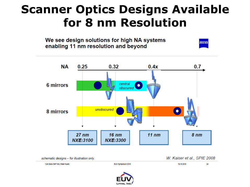
Scanner Optics Designs Available for 8 nm Resolution
EUV RESIST STATUS
EUVL Technology Status
50
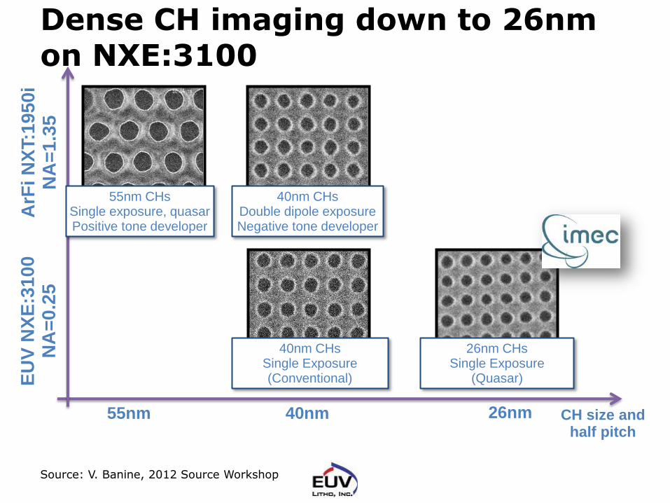
Dense CH imaging down to 26nm on NXE:3100
ArF
i N
XT:1
95
0i
NA
=1
.35
E
UV
NX
E:3
10
0
NA
=0
.25
55nm 40nm 26nm
55nm CHs Single exposure, quasar Positive tone developer
40nm CHs Double dipole exposure Negative tone developer
40nm CHs Single Exposure (Conventional)
26nm CHs Single Exposure
(Quasar)
CH size and half pitch
Source: V. Banine, 2012 Source Workshop
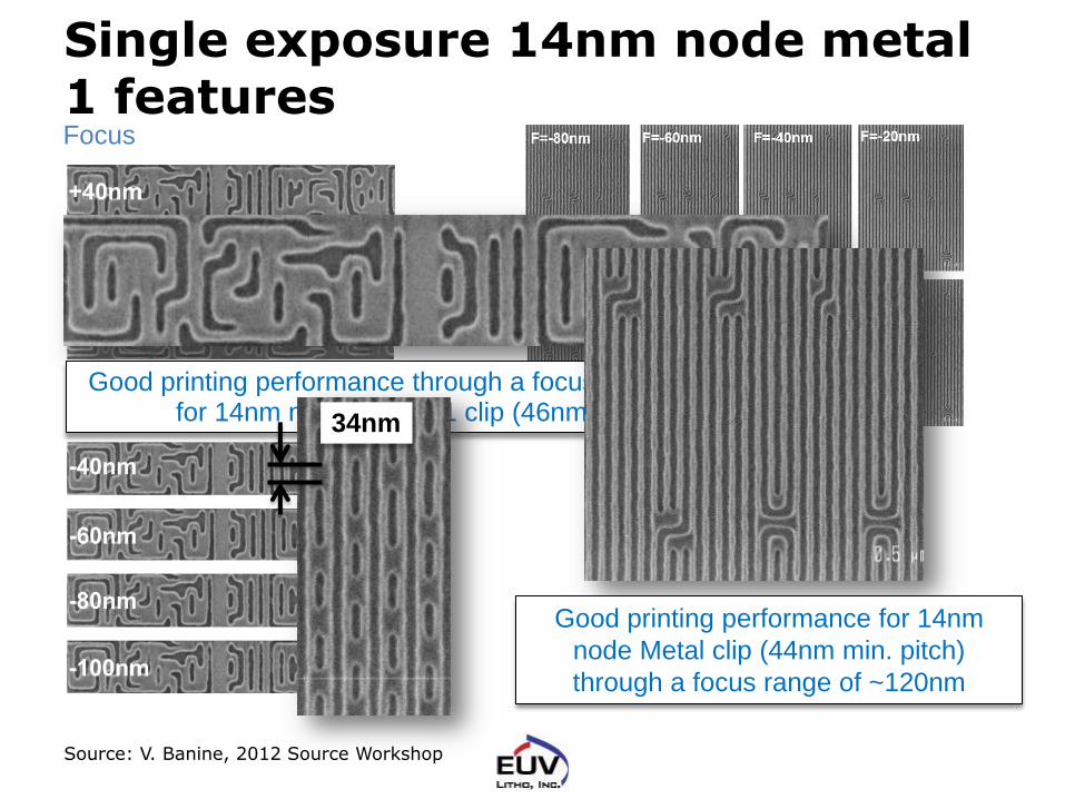
Single exposure 14nm node metal 1 features Focus
Good printing performance through a focus range of ~100nm for 14nm node ARM M1 clip (46nm min. pitch)
Good printing performance for 14nm
node Metal clip (44nm min. pitch)
through a focus range of ~120nm
34nm
Source: V. Banine, 2012 Source Workshop

LWR remains the leading challenge for EUV resists
53 Source: S. Wurm, 2012 Semicon West

Resolution OK but sensitivity needs to improve by 2 to 3 x
54 Source: S. Wurm, 2012 Semicon West

LER of ~3.2 nm for 25 nm L/S via Post Processing
55

EUV SCANNER STATUS
EUVL Technology Status
56
Slide 57
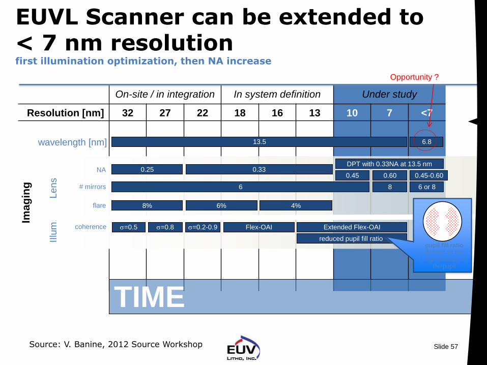
EUVL Scanner can be extended to < 7 nm resolution first illumination optimization, then NA increase
On-site / in integration In system definition Under study
Resolution [nm] 32 27 22 18 16 13 10 7 <7
layo
ut
NA 0.25 0.33 0.45 0.60 0.45-0.60
# mirrors 6 8 6 or 8
wavelength [nm] 13.5 6.8
Lens
flare 8% 6% 4%
IIlu
m.
Flex-OAI s=0.8 Extended Flex-OAI
reduced pupil fill ratio
DPT with 0.33NA at 13.5 nm
Imag
ing
s=0.5 s=0.2-0.9 coherence
TIME
pupil fill ratio defined as the
bright fraction of the pupil
Opportunity ?
Source: V. Banine, 2012 Source Workshop
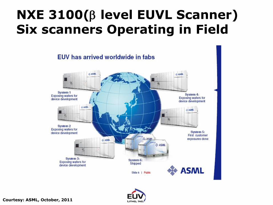
NXE 3100(b level EUVL Scanner) Six scanners Operating in Field
Courtesy: ASML, October, 2011
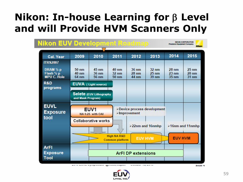
Nikon: In-house Learning for b Level and will Provide HVM Scanners Only
59
EUVL STATUS SUMMARY
EUVL Technology Status
60
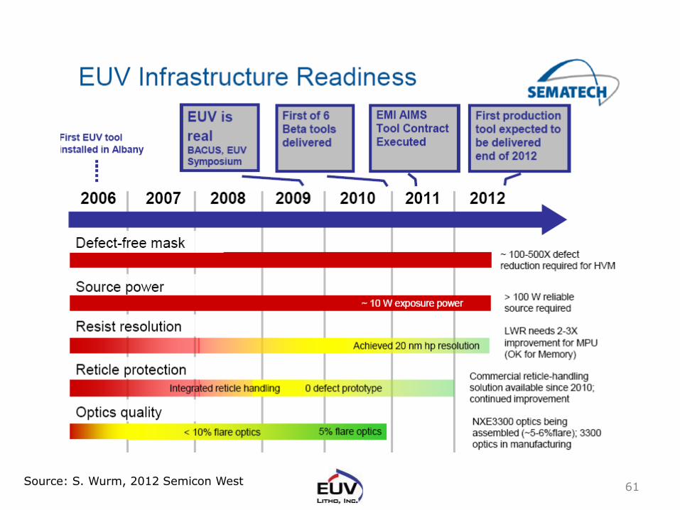
61 Source: S. Wurm, 2012 Semicon West

Optical Lithography Challenges (ITRS 2011) • Near Term Challenges (2011-18)
– EUV source power to meet throughput requirement
– Defect "free" EUV masks availability mask infrastructure availability
– EUV mask in fab handling, storage, and requalification.
– Resist at 16nm and below that can meet sensitivity, resolution, LER requirements
– Retooling requirements for 450mm transition
62
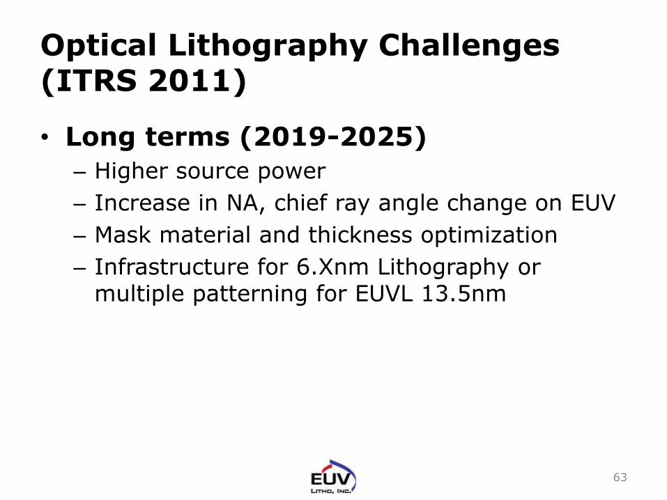
Optical Lithography Challenges (ITRS 2011) • Long terms (2019-2025)
– Higher source power
– Increase in NA, chief ray angle change on EUV
– Mask material and thickness optimization
– Infrastructure for 6.Xnm Lithography or multiple patterning for EUVL 13.5nm
63
Outline
• Introduction to EUV Lithography
• Technical Status and Challenges
• Summary
Summary
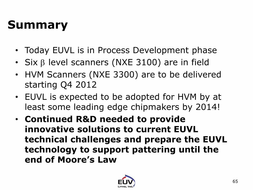
• Today EUVL is in Process Development phase
• Six b level scanners (NXE 3100) are in field
• HVM Scanners (NXE 3300) are to be delivered starting Q4 2012
• EUVL is expected to be adopted for HVM by at least some leading edge chipmakers by 2014!
• Continued R&D needed to provide innovative solutions to current EUVL technical challenges and prepare the EUVL technology to support pattering until the end of Moore’s Law
65