ETSI EN 301 908-2 V5.4 · 4.2.2.1A Definition for DC-HSUPA ... History ... 6 ETSI EN 301 908-2...
45
ETSI EN 301 908-2 V5.4.1 (2012-12) IMT cellular networks; Harmonized EN covering the essential requirements of article 3.2 of the R&TTE Directive; Part 2: CDMA Direct Spread (UTRA FDD) User Equipment (UE) Harmonized European Standard
Transcript of ETSI EN 301 908-2 V5.4 · 4.2.2.1A Definition for DC-HSUPA ... History ... 6 ETSI EN 301 908-2...

ETSI EN 301 908-2 V5.4.1 (2012-12)
IMT cellular networks; Harmonized EN covering the essential requirements
of article 3.2 of the R&TTE Directive; Part 2: CDMA Direct Spread (UTRA FDD) User Equipment (UE)
Harmonized European Standard

ETSI
ETSI EN 301 908-2 V5.4.1 (2012-12) 2
Reference REN/MSG-TFES-006-2-2
Keywords 3G, 3GPP, cellular, digital, IMT, mobile, radio,
regulation, UMTS, UTRA, WCDMA
ETSI
650 Route des Lucioles F-06921 Sophia Antipolis Cedex - FRANCE
Tel.: +33 4 92 94 42 00 Fax: +33 4 93 65 47 16
Siret N° 348 623 562 00017 - NAF 742 C
Association à but non lucratif enregistrée à la Sous-Préfecture de Grasse (06) N° 7803/88
Important notice
Individual copies of the present document can be downloaded from: http://www.etsi.org
The present document may be made available in more than one electronic version or in print. In any case of existing or perceived difference in contents between such versions, the reference version is the Portable Document Format (PDF).
In case of dispute, the reference shall be the printing on ETSI printers of the PDF version kept on a specific network drive within ETSI Secretariat.
Users of the present document should be aware that the document may be subject to revision or change of status. Information on the current status of this and other ETSI documents is available at
http://portal.etsi.org/tb/status/status.asp
If you find errors in the present document, please send your comment to one of the following services: http://portal.etsi.org/chaircor/ETSI_support.asp
Copyright Notification
No part may be reproduced except as authorized by written permission. The copyright and the foregoing restriction extend to reproduction in all media.
© European Telecommunications Standards Institute 2012.
All rights reserved.
DECTTM, PLUGTESTSTM, UMTSTM and the ETSI logo are Trade Marks of ETSI registered for the benefit of its Members. 3GPPTM and LTE™ are Trade Marks of ETSI registered for the benefit of its Members and
of the 3GPP Organizational Partners. GSM® and the GSM logo are Trade Marks registered and owned by the GSM Association.

ETSI
ETSI EN 301 908-2 V5.4.1 (2012-12) 3
Contents
Intellectual Property Rights ................................................................................................................................ 6
Foreword ............................................................................................................................................................. 6
Introduction ........................................................................................................................................................ 7
1 Scope ........................................................................................................................................................ 8
2 References ................................................................................................................................................ 9
2.1 Normative references ......................................................................................................................................... 9
2.2 Informative references ........................................................................................................................................ 9
3 Definitions, symbols and abbreviations ................................................................................................. 10
3.1 Definitions ........................................................................................................................................................ 10
3.2 Symbols ............................................................................................................................................................ 11
3.3 Abbreviations ................................................................................................................................................... 12
4 Technical requirements specifications ................................................................................................... 13
4.1 Environmental profile ....................................................................................................................................... 13
4.2 Conformance requirements .............................................................................................................................. 13
4.2.1 Introduction................................................................................................................................................. 13
4.2.2 Transmitter maximum output power........................................................................................................... 14
4.2.2.1 Definition .............................................................................................................................................. 14
4.2.2.1A Definition for DC-HSUPA .................................................................................................................... 14
4.2.2.2 Limits .................................................................................................................................................... 14
4.2.2.3 Limits for DC-HSUPA .......................................................................................................................... 14
4.2.2.3A Conformance. ........................................................................................................................................ 15
4.2.3 Transmitter spectrum emission mask .......................................................................................................... 15
4.2.3.1 Definition .............................................................................................................................................. 15
4.2.3.1A Definition for DC-HSUPA .................................................................................................................... 15
4.2.3.2 Limits .................................................................................................................................................... 16
4.2.3.2A Limits for DC-HSUPA .......................................................................................................................... 16
4.2.3.3 Conformance ......................................................................................................................................... 16
4.2.4 Transmitter spurious emissions ................................................................................................................... 17
4.2.4.1 Definition .............................................................................................................................................. 17
4.2.4.1A Definition for DC-HSUPA .................................................................................................................... 17
4.2.4.2 Limits .................................................................................................................................................... 17
4.2.4.2A Limits for DC-HSUPA .......................................................................................................................... 18
4.2.4.3 Conformance ......................................................................................................................................... 20
4.2.5 Transmitter minimum output power ........................................................................................................... 20
4.2.5.1 Definition .............................................................................................................................................. 20
4.2.5.1A Definition for DC-HSUPA .................................................................................................................... 20
4.2.5.2 Limits .................................................................................................................................................... 20
4.2.5.2A Limits for DC-HSUPA .......................................................................................................................... 21
4.2.5.3 Conformance ......................................................................................................................................... 21
4.2.6 Receiver Adjacent Channel Selectivity (ACS) ........................................................................................... 21
4.2.6.1 Definition .............................................................................................................................................. 21
4.2.6.2 Limits .................................................................................................................................................... 21
4.2.6.3 Conformance ......................................................................................................................................... 21
4.2.7 Receiver blocking characteristics ............................................................................................................... 21
4.2.7.1 Definition .............................................................................................................................................. 21
4.2.7.2 Limits .................................................................................................................................................... 21
4.2.7.3 Conformance ......................................................................................................................................... 23
4.2.8 Receiver spurious response ......................................................................................................................... 23
4.2.8.1 Definition .............................................................................................................................................. 23
4.2.8.2 Limits .................................................................................................................................................... 23
4.2.8.3 Conformance ......................................................................................................................................... 24
4.2.9 Receiver intermodulation characteristics .................................................................................................... 24
4.2.9.1 Definition .............................................................................................................................................. 24

ETSI
ETSI EN 301 908-2 V5.4.1 (2012-12) 4
4.2.9.2 Limits .................................................................................................................................................... 24
4.2.9.3 Conformance ......................................................................................................................................... 24
4.2.10 Receiver spurious emissions ....................................................................................................................... 25
4.2.10.1 Definition .............................................................................................................................................. 25
4.2.10.2 Limits .................................................................................................................................................... 25
4.2.10.3 Conformance ......................................................................................................................................... 26
4.2.11 Out-of-synchronization handling of output power ...................................................................................... 26
4.2.11.1 Definition .............................................................................................................................................. 26
4.2.11.2 Limits .................................................................................................................................................... 26
4.2.11.3 Conformance ......................................................................................................................................... 28
4.2.12 Transmitter Adjacent Channel Leakage power Ratio (ACLR) ................................................................... 28
4.2.12.1 Definition .............................................................................................................................................. 28
4.2.12.1A Definition for DC-HSUPA .................................................................................................................... 28
4.2.12.2 Limits .................................................................................................................................................... 28
4.2.12.2A Limits for DC-HSUPA .......................................................................................................................... 28
4.2.12.3 Conformance ......................................................................................................................................... 28
5 Testing for compliance with technical requirements .............................................................................. 29
5.1 Environmental conditions for testing ............................................................................................................... 29
5.2 Interpretation of the measurement results ........................................................................................................ 29
5.3 Essential radio test suites .................................................................................................................................. 30
5.3.1 Transmitter maximum output power........................................................................................................... 30
5.3.1.1 Method of test ....................................................................................................................................... 30
5.3.1.1.1 Initial conditions .............................................................................................................................. 30
5.3.1.1.1A Initial conditions for DC-HSUPA ................................................................................................... 31
5.3.1.1.2 Procedure ......................................................................................................................................... 31
5.3.1.1.2A Procedure for DC-HSUPA .............................................................................................................. 31
5.3.1.2 Test requirements .................................................................................................................................. 31
5.3.2 Transmitter spectrum emission mask .......................................................................................................... 31
5.3.2.1 Method of test ....................................................................................................................................... 31
5.3.2.1.1 Initial conditions for UEs not supporting HSDPA and/or E-DCH .................................................. 31
5.3.2.1.1A Initial conditions for UEs supporting HSDPA and/or E-DCH ........................................................ 32
5.3.2.1.1B Initial conditions for DC-HSUPA ................................................................................................... 32
5.3.2.1.2 Procedure for UEs not supporting HSDPA and/or E-DCH ............................................................. 32
5.3.2.1.2A Procedure for UEs supporting HSDPA and/or E-DCH ................................................................... 32
5.3.2.1.2B Procedure for DC-HSUPA .............................................................................................................. 32
5.3.2.2 Test requirements .................................................................................................................................. 33
5.3.3 Transmitter spurious emissions ................................................................................................................... 33
5.3.3.1 Method of test ....................................................................................................................................... 33
5.3.3.1.1 Initial conditions .............................................................................................................................. 33
5.3.3.1.1A Initial conditions for DC-HSUPA ................................................................................................... 33
5.3.3.1.2 Procedure ......................................................................................................................................... 33
5.3.3.1.2A Procedure for DC-HSUPA .............................................................................................................. 33
5.3.3.2 Test requirements .................................................................................................................................. 34
5.3.4 Transmitter minimum output power ........................................................................................................... 34
5.3.4.1 Method of test ....................................................................................................................................... 34
5.3.4.1.1 Initial conditions .............................................................................................................................. 34
5.3.4.1.1A Initial conditions for DC-HSUPA ................................................................................................... 34
5.3.4.1.2 Procedure ......................................................................................................................................... 34
5.3.4.1.2A Procedure for DC-HSUPA .............................................................................................................. 34
5.3.4.2 Test requirements .................................................................................................................................. 34
5.3.5 Receiver Adjacent Channel Selectivity (ACS) ........................................................................................... 35
5.3.5.1 Method of test ....................................................................................................................................... 35
5.3.5.1.1 Initial conditions .............................................................................................................................. 35
5.3.5.1.2 Procedure ......................................................................................................................................... 35
5.3.5.2 Test requirements .................................................................................................................................. 35
5.3.6 Receiver blocking characteristics ............................................................................................................... 35
5.3.6.1 Method of test ....................................................................................................................................... 35
5.3.6.1.1 Initial requirements .......................................................................................................................... 35
5.3.6.1.2 Procedure ......................................................................................................................................... 36
5.3.6.2 Test requirements .................................................................................................................................. 36
5.3.7 Receiver spurious response ......................................................................................................................... 36

ETSI
ETSI EN 301 908-2 V5.4.1 (2012-12) 5
5.3.7.1 Method of test ....................................................................................................................................... 36
5.3.7.1.1 Initial conditions .............................................................................................................................. 36
5.3.7.1.2 Procedure ......................................................................................................................................... 36
5.3.7.2 Test requirements .................................................................................................................................. 36
5.3.8 Receiver Intermodulation characteristics .................................................................................................... 36
5.3.8.1 Method of test ....................................................................................................................................... 36
5.3.8.1.1 Initial conditions .............................................................................................................................. 36
5.3.8.1.2 Procedure ......................................................................................................................................... 37
5.3.8.2 Test requirements .................................................................................................................................. 37
5.3.9 Receiver spurious emissions ....................................................................................................................... 37
5.3.9.1 Method of test ....................................................................................................................................... 37
5.3.9.1.1 Initial conditions .............................................................................................................................. 37
5.3.9.1.2 Procedure ......................................................................................................................................... 37
5.3.9.2 Test requirements .................................................................................................................................. 37
5.3.10 Out-of-synchronization handling of output power ...................................................................................... 37
5.3.10.1 Method of test ....................................................................................................................................... 37
5.3.10.1.1 Initial conditions .............................................................................................................................. 37
5.3.10.1.2 Procedure ......................................................................................................................................... 38
5.3.10.2 Test requirements .................................................................................................................................. 38
5.3.11 Transmitter adjacent channel leakage power ratio ...................................................................................... 38
5.3.11.1 Method of test ....................................................................................................................................... 38
5.3.11.1.1 Initial conditions for UEs not supporting HSDPA and/or E-DCH .................................................. 38
5.3.11.1.1A Initial conditions for UEs supporting HSDPA and/or E-DCH ........................................................ 38
5.3.11.1.1B Initial conditions for DC-HSUPA ................................................................................................... 39
5.3.11.1.2 Procedure for UEs not supporting HSDPA and/or E-DCH ............................................................. 39
5.3.11.1.2A Procedure for UEs supporting HSDPA and/or E-DCH ................................................................... 39
5.3.11.1.2B Procedure for DC-HSUPA .............................................................................................................. 39
5.3.11.2 Test requirements .................................................................................................................................. 39
Annex A (normative): HS Requirements and conformance Test specifications Table (HS-RTT) ........................................................................................................ 40
Annex B (normative): Environmental profile ................................................................................... 42
B.1 General ................................................................................................................................................... 42
B.1.1 Introduction ...................................................................................................................................................... 42
B.1.2 Temperature ..................................................................................................................................................... 42
B.1.3 Voltage ............................................................................................................................................................. 42
B.1.4 Test environment .............................................................................................................................................. 43
Annex C (informative): Bibliography ................................................................................................... 44
History .............................................................................................................................................................. 45

ETSI
ETSI EN 301 908-2 V5.4.1 (2012-12) 6
Intellectual Property Rights IPRs essential or potentially essential to the present document may have been declared to ETSI. The information pertaining to these essential IPRs, if any, is publicly available for ETSI members and non-members, and can be found in ETSI SR 000 314: "Intellectual Property Rights (IPRs); Essential, or potentially Essential, IPRs notified to ETSI in respect of ETSI standards", which is available from the ETSI Secretariat. Latest updates are available on the ETSI Web server (http://ipr.etsi.org).
Pursuant to the ETSI IPR Policy, no investigation, including IPR searches, has been carried out by ETSI. No guarantee can be given as to the existence of other IPRs not referenced in ETSI SR 000 314 (or the updates on the ETSI Web server) which are, or may be, or may become, essential to the present document.
Foreword This Harmonized European Standard (EN) has been produced by ETSI Technical Committee Mobile Standards Group (MSG).
The present document has been produced by ETSI in response to mandate M/284 from the European Commission issued under Directive 98/34/EC [i.1] as amended by Directive 98/48/EC [i.10].
The title and reference to the present document are intended to be included in the publication in the Official Journal of the European Union of titles and references of Harmonized Standard under the Directive 1999/5/EC [i.2].
See article 5.1 of Directive 1999/5/EC [i.2] for information on presumption of conformity and Harmonised Standards or parts thereof the references of which have been published in the Official Journal of the European Union.
The requirements relevant to Directive 1999/5/EC [i.2] are summarised in annex A.
The present document is part 2 of a multi-part deliverable covering the essential requirements under article 3.2 of Directive 1999/5/EC [i.2] (R&TTE Directive) for Base Stations (BS), Repeaters and User Equipment (UE) for IMT cellular networks, as identified below:
Part 1: "Introduction and common requirements";
Part 2: "CDMA Direct Spread (UTRA FDD) User Equipment (UE)";
Part 3: "CDMA Direct Spread (UTRA FDD) Base Stations (BS)";
Part 4: "CDMA Multi-Carrier (cdma2000) User Equipment (UE)";
Part 5: "CDMA Multi-Carrier (cdma2000) Base Stations (BS)";
Part 6: "CDMA TDD (UTRA TDD) User Equipment (UE)";
Part 7: "CDMA TDD (UTRA TDD) Base Stations (BS)";
Part 8: "Harmonized EN for IMT-2000, TDMA Single-Carrier (UWC 136) (UE) covering essential requirements of article 3.2 of the R&TTE Directive";
Part 9: "Harmonized EN for IMT-2000, TDMA Single-Carrier (UWC 136) (BS) covering essential requirements of article 3.2 of the R&TTE Directive";
Part 10: "Harmonized EN for IMT-2000, FDMA/TDMA (DECT) covering essential requirements of article 3.2 of the R&TTE Directive";
Part 11: "CDMA Direct Spread (UTRA FDD) (Repeaters)";
Part 12: "Harmonized EN for IMT-2000, CDMA Multi-Carrier (cdma2000) (Repeaters) covering the essential requirements of article 3.2 of the R&TTE Directive";
Part 13: "Evolved Universal Terrestrial Radio Access (E-UTRA) User Equipment (UE)";

ETSI
ETSI EN 301 908-2 V5.4.1 (2012-12) 7
Part 14: "Evolved Universal Terrestrial Radio Access (E-UTRA) Base Stations (BS)";
Part 15: "Evolved Universal Terrestrial Radio Access (E-UTRA FDD) (Repeaters)";
Part 16: "Harmonized EN for IMT-2000, Evolved CDMA Multi-Carrier Ultra Mobile Broadband (UMB) (UE) covering the essential requirements of article 3.2 of the R&TTE Directive";
Part 17: "Harmonized EN for IMT-2000, Evolved CDMA Multi-Carrier Ultra Mobile Broadband (UMB) (BS) covering the essential requirements of article 3.2 of the R&TTE Directive";
Part 18: "E-UTRA, UTRA and GSM/EDGE Multi-Standard Radio (MSR) Base Station (BS)";
Part 19: "OFDMA TDD WMAN (Mobile WiMAX) TDD User Equipment (UE)";
Part 20: "OFDMA TDD WMAN (Mobile WiMAX) TDD Base Stations (BS)";
Part 21: "OFDMA TDD WMAN (Mobile WiMAX) FDD User Equipment (UE)";
Part 22: "OFDMA TDD WMAN (Mobile WiMAX) FDD Base Stations (BS)".
National transposition dates
Date of adoption of this EN: 17 December 2012
Date of latest announcement of this EN (doa): 31 March 2013
Date of latest publication of new National Standard or endorsement of this EN (dop/e):
30 September 2013
Date of withdrawal of any conflicting National Standard (dow): 30 September 2014
Introduction The present document is part of a set of standards developed by ETSI and is designed to fit in a modular structure to cover all radio and telecommunications terminal equipment within the scope of the R&TTE Directive [i.2]. The modular structure is shown in EG 201 399 [i.3].

ETSI
ETSI EN 301 908-2 V5.4.1 (2012-12) 8
1 Scope The present document applies to the following radio equipment type:
• User Equipment for IMT-2000 CDMA Direct Spread (UTRA FDD).
These radio equipment types are capable of operating in all or any part of the frequency bands given in table 1-1.
Table 1-1: UTRA FDD operating bands
UTRA FDD Band Direction of transmission UTRA FDD operating bands I Transmit 1 920 MHz to 1 980 MHz
Receive 2 110 MHz to 2 170 MHz III Transmit 1 710 MHz to 1 785 MHz
Receive 1 805 MHz to 1 880 MHz VII Transmit 2 500 MHz to 2 570 MHz
Receive 2 620 MHz to 2 690 MHz VIII Transmit 880 MHz to 915 MHz
Receive 925 MHz to 960 MHz XV Transmit 1 900 MHz to 1 920 MHz
Receive 2 600 MHz to 2 620 MHz XVI Transmit 2 010 MHz to 2 025 MHz
Receive 2 585 MHz to 2 600 MHz XX Transmit 832 MHz to 862 MHz
Receive 791 MHz to 821 MHz
The present document covers requirements for UTRA FDD User Equipment from 3GPP Releases 99, 4, 5, 6, 7, 8, and 9. In addition, the present document covers requirements for UTRA FDD User Equipment in the operating bands specified in TS 102 735 [i.4].
NOTE 1: For Band XX:
- for user equipment designed to be mobile or nomadic, the requirements in the present document measured at the antenna port also show conformity to the corresponding requirement defined as TRP (Total Radiated Power), as described in Commission Decision 2010/267/EU [i.7], ECC Decision (09)03 [i.8] and CEPT Report 30 [i.9];
- for user equipment designed to be fixed or installed, the present document does not address the requirements described in Commission Decision 2010/267/EU [i.7], ECC Decision (09)03 [i.8] and CEPT Report 30 [i.9].
The present document is intended to cover the provisions of Directive 1999/5/EC [i.2] (R&TTE Directive) article 3.2, which states that "radio equipment shall be so constructed that it effectively uses the spectrum allocated to terrestrial/space radio communications and orbital resources so as to avoid harmful interference".
In addition to the present document, other ENs that specify technical requirements in respect of essential requirements under other parts of article 3 of the R&TTE Directive [i.2] may apply to equipment within the scope of the present document.
NOTE 2: A list of such ENs is included on the web site http://www.newapproach.org/.

ETSI
ETSI EN 301 908-2 V5.4.1 (2012-12) 9
2 References References are either specific (identified by date of publication and/or edition number or version number) or non-specific. For specific references, only the cited version applies. For non-specific references, the latest version of the reference document (including any amendments) applies.
Referenced documents which are not found to be publicly available in the expected location might be found at http://docbox.etsi.org/Reference.
NOTE: While any hyperlinks included in this clause were valid at the time of publication ETSI cannot guarantee their long term validity.
2.1 Normative references The following referenced documents are necessary for the application of the present document.
[1] Void.
[2] ETSI TS 134 121-1 (V10.3.0) (08/2012): "Universal Mobile Telecommunications System (UMTS); User Equipment (UE) conformance specification; Radio transmission and reception (FDD); Part 1: Conformance specification (3GPP TS 34.121-1 version 10.3.0 Release 10)".
[3] ETSI TS 134 108 (V11.3.0) (10/2012): "Universal Mobile Telecommunications System (UMTS); LTE; Common test environments for User Equipment (UE); Conformance testing (3GPP TS 34.108 version 11.3.0 Release 11)".
[4] ETSI TS 134 109 (V10.1.0) (01/2012): "Universal Mobile Telecommunications System (UMTS); Terminal logical test interface; Special conformance testing functions (3GPP TS 34.109 version 10.1.0 Release 10)".
[5] ETSI TS 125 101 (V9.9.0) (07/2012): "Universal Mobile Telecommunications System (UMTS); User Equipment (UE) radio transmission and reception (FDD) (3GPP TS 25.101 version 9.9.0 Release 9)".
[6] IEC 60068-2-1 (03/2007): "Environmental testing - Part 2-1: Tests - Test A: Cold".
[7] IEC 60068-2-2 (07/2007): "Environmental testing - Part 2-2: Tests - Test B: Dry heat".
[8] ETSI TS 125 214 (V9.8.0) (03/2012): "Universal Mobile Telecommunications System (UMTS); Physical layer procedures (FDD) (3GPP TS 25.214 version 9.8.0 Release 9)".
[9] ETSI TS 145 004 (V9.1.0) (07/2010): "Digital cellular telecommunications system (Phase 2+); Modulation (3GPP TS 45.004 version 9.1.0 Release 9)".
[10] ETSI EN 301 908-1 (V5.2.1) (05/2011): "IMT cellular networks; Harmonized EN covering the essential requirements of article 3.2 of the R&TTE Directive; Part 1: Introduction and common requirements".
2.2 Informative references The following referenced documents are not necessary for the application of the present document but they assist the user with regard to a particular subject area.
[i.1] Directive 98/34/EC of the European Parliament and of the Council of 22 June 1998 laying down a procedure for the provision of information in the field of technical standards and regulations.
[i.2] Directive 1999/5/EC of the European Parliament and of the Council of 9 March 1999 on radio equipment and telecommunications terminal equipment and the mutual recognition of their conformity (R&TTE Directive).
[i.3] ETSI EG 201 399: "Electromagnetic compatibility and Radio spectrum Matters (ERM); A guide to the production of Harmonized Standards for application under the R&TTE Directive".

ETSI
ETSI EN 301 908-2 V5.4.1 (2012-12) 10
[i.4] ETSI TS 102 735 (V7.1.0): "Universal Mobile Telecommunications System (UMTS); Band-specific requirements for UMTS Frequency Division Duplex (FDD) operation in the bands 1 900 MHz to 1 920 MHz paired with 2 600 MHz to 2 620 MHz and 2 010 MHz to 2 025 MHz paired with 2 585 MHz to 2 600 MHz".
[i.5] Void.
[i.6] ETSI TR 100 028 (all parts) (V1.4.1): "Electromagnetic compatibility and Radio spectrum Matters (ERM); Uncertainties in the measurement of mobile radio equipment characteristics".
[i.7] Commission Decision of 6 May 2010 on harmonised technical conditions of use in the 790-862 MHz frequency band for terrestrial systems capable of providing electronic communications services in the European Union (2010/267/EU).
[i.8] ECC Decision of 30 October 2009 on harmonised conditions for mobile/fixed communications networks (MFCN) operating in the band 790 - 862 MHz (ECC/DEC/(09)03).
[i.9] CEPT Report 30 of 30 October 2009 to the European Commission in response to the Mandate on "The identification of common and minimal (least restrictive) technical conditions for 790 - 862 MHz for the digital dividend in the European Union".
[i.10] Directive 98/48/EC of the European Parliament and of the Council of 20 July 1998 amending Directive 98/34/EC laying down a procedure for the provision of information in the field of technical standards and regulations.
3 Definitions, symbols and abbreviations
3.1 Definitions For the purposes of the present document, the following terms and definitions apply:
chip rate: rate of "chips" (modulated symbols after spreading) per second
NOTE: The UTRA FDD chip rate is 3,84 Mchip/s.
data rate: rate of the user information, which is transmitted over the Air Interface
EXAMPLE: Output rate of the voice codec.
environmental profile: range of environmental conditions under which equipment within the scope of the present document is required to comply with the provisions of the present document
maximum output power: measure of the maximum power the UE can transmit (i.e. the actual power as would be measured assuming no measurement error) in a bandwidth of at least (1 + α) times the chip rate of the radio access mode
NOTE: The period of measurement is assumed to be at least one timeslot.
mean power: power (transmitted or received) in a bandwidth of at least (1 + α) times the chip rate of the radio access mode, when applied to a WCDMA modulated signal
NOTE: The period of measurement is assumed to be at least one timeslot unless otherwise stated.
node B: logical node responsible for radio transmission/reception in one or more cells to/from the User Equipment
nominal maximum output power: nominal power defined by the UE power class

ETSI
ETSI EN 301 908-2 V5.4.1 (2012-12) 11
operating band: frequency range that is defined with a specific set of technical requirements, in which UTRA FDD operates
NOTE: Operating bands for UTRA are designated with Roman numerals, while the corresponding operating bands for E-UTRA are designated with Arabic numerals.
power spectral density: function of power versus frequency and when integrated across a given bandwidth, the function represents the mean power in such a bandwidth
NOTE 1: When the mean power is normalized to (divided by) the chip-rate it represents the mean energy per chip. Some signals are directly defined in terms of energy per chip, (DPCH_Ec, Ec, OCNS_Ec and S-CCPCH_Ec) and others defined in terms of PSD (Io, Ioc, Ior and Îor). There also exist quantities that
are a ratio of energy per chip to PSD (DPCH_Ec/Ior, Ec/Ior, etc.). This is the common practice of relating
energy magnitudes in communication systems.
NOTE 2: It can be seen that if both energy magnitudes in the ratio are divided by time, the ratio is converted from an energy ratio to a power ratio, which is more useful from a measurement point of view. It follows that an energy per chip of X dBm/3,84 MHz can be expressed as a mean power per chip of X dBm. Similarly, a signal PSD of Y dBm/3,84 MHz can be expressed as a signal power of Y dBm.
NOTE 3: The units of Power Spectral Density (PSD) are extensively used in the present document.
RRC filtered mean power: mean power as measured through a root raised cosine filter with roll-off factor α and a bandwidth equal to the chip rate of the radio access mode
NOTE: The RRC filtered mean power of a perfectly modulated WCDMA signal is 0,246 dB lower than the mean power of the same signal.
3.2 Symbols For the purposes of the present document, the following symbols apply:
α Roll-off factor of the root raised cosine filter, α = 0,22 DPCH_Ec Average energy per PN chip for DPCH Ec Average energy per PN chip
Fuw Frequency of unwanted signal
NOTE: This is specified in bracket in terms of an absolute frequency(s) or a frequency offset from the assigned channel frequency.
oI The total received power spectral density, including signal and interference, as measured at the UE
antenna connector
ocI Power spectral density (integrated in a noise bandwidth equal to the chip rate and normalized to
the chip rate) of a band limited white noise source (simulating interference from cells, which are not defined in a test procedure) as measured at the UE antenna connector
orI Total transmit power spectral density (integrated in a bandwidth of (1 + α) times the chip rate and
normalized to the chip rate) of the downlink signal at the Node B antenna connector
orI Received power spectral density (integrated in a bandwidth of (1 + α) times the chip rate and
normalized to the chip rate) of the downlink signal as measured at the UE antenna connector βc Gain factor for DPCCH
βd Gain factor for DPDCH
βhs Gain factor for HS-DPCCH
βec Gain factor for E-DPCCH
βed Gain factor for E-DPDCH

ETSI
ETSI EN 301 908-2 V5.4.1 (2012-12) 12
3.3 Abbreviations For the purposes of the present document, the following abbreviations apply:
AC Access Channel ACLR Adjacent Channel Leakage power Ratio ACS Adjacent Channel Selectivity BER Bit Error Ratio BS Base Station CDMA Code Division Multiple Access CW Continuous Wave
NOTE: Unmodulated signal.
DC-HSUPA Dual Cell HSUPA DCH Dedicated Channel
NOTE: Which is mapped into Dedicated Physical Channel.
DL Downlink DPCCH Dedicated Physical Control CHannel DPCH Dedicated Physical Channel DPDCH Dedicated Physical Data CHannel E-DCH Enhanced Dedicated Channel E-DPCCH Enhanced DPCCH E-DPDCH Enhanced DPDCH EMC ElectroMagnetic Compatibility ERM Electromagnetic compatibility and Radio spectrum Matters EU European Union EUT Equipment Under Test FDD Frequency Division Duplex GMSK Gaussian Minimum Shift Keying GSM Global System for Mobile HS-DPCCH High Speed DPCCH HSDPA High Speed Downlink Packet Access HSUPA High Speed Uplink Packet Access IMT International Mobile Telecommunications LTE Long Term Evolution MPR Maximum Power Reduction MSG Mobile Standards Group MSR Multi-Standard Radio OCNS Orthogonal Channel Noise Simulator
NOTE: A mechanism used to simulate the users or control signals on the other orthogonal channels of a downlink.
OFDMA Orthogonal Frequency Division Multiple Access PCH Paging Channel PN PseudoNoise PSD Power Spectral Density REFSENS Reference sensitivity RF Radio Frequency RRC Root Raised Cosine R&TTE Radio and Telecommunications Terminal Equipment SS System Simulator
NOTE: See TS 134 121-1 [2].
TDD Time Division Duplex TDMA Time Division Multiple Access TFES Task Force for European Standards for IMT TH Temperature High TH/VH High extreme Temperature/High extreme Voltage

ETSI
ETSI EN 301 908-2 V5.4.1 (2012-12) 13
TH/VL High extreme Temperature/Low extreme Voltage TL Temperature Low TL/VH Low extreme Temperature/High extreme Voltage TL/VL Low extreme Temperature/Low extreme Voltage TPC Transmit Power Control TRP Total Radiated Power UARFCN UTRA Absolute Radio Frequency Channel Number UE User Equipment UL Uplink UMB Ultra Mobile Broadband UMTS Universal Mobile Telecommunications System UTRA Universal Terrestrial Radio Access VH Higher extreme Voltage VL Lower extreme Voltage WCDMA Wideband Code Division Multiple Access WMAN Wireless Metropolitan Area Network
4 Technical requirements specifications
4.1 Environmental profile The technical requirements of the present document apply under the environmental profile for operation of the equipment, which shall be declared by the supplier. The equipment shall comply with all the technical requirements of the present document at all times when operating within the boundary limits of the declared operational environmental profile.
For guidance on how a supplier can declare the environmental profile see annex B.
4.2 Conformance requirements The requirements in the present document are based on the assumption that the operating band (i.e. band I, III, VII, VIII, XV, XVI and XX) is shared between systems of the IMT family (for band III and VIII also GSM) or systems having compatible characteristics.
4.2.1 Introduction
To meet the essential requirement under article 3.2 of the Directive 1999/5/EC [i.2] (R&TTE Directive) for IMT User Equipment (UE) eight essential parameters in addition to those in EN 301 908-1 [10] have been identified. Table 4.2.1-1 provides a cross reference between these eight essential parameters and the corresponding eleven technical requirements for equipment within the scope of the present document.
Table 4.2.1-1: Cross references
Essential parameter Corresponding technical requirements Spectrum emissions mask 4.2.3 Transmitter Spectrum emissions mask
4.2.12 Transmitter adjacent channel leakage power ratio Conducted spurious emissions in active mode 4.2.4 Transmitter spurious emissions Accuracy of maximum output power 4.2.2 Transmitter maximum output power Prevention of harmful interference through control of power
4.2.5 Transmitter minimum output power
Conducted spurious emission in idle mode 4.2.10 Receiver spurious emissions Impact of interference on receiver performance 4.2.7 Receiver Blocking characteristics
4.2.8 Receiver spurious response 4.2.9 Receiver Intermodulation characteristics
Receiver adjacent channel selectivity 4.2.6 Receiver Adjacent Channel Selectivity (ACS) Control and Monitoring functions 4.2.11 Out of synchronization handling of output power

ETSI
ETSI EN 301 908-2 V5.4.1 (2012-12) 14
The technical requirements in the present document apply for UEs supporting UTRA FDD in declared operating bands. The technical requirements for HSDPA and E-DCH shall apply only to UEs supporting these features. The technical requirements for DC-HSUPA shall apply only to UEs supporting this feature.
Unless otherwise stated, the transmitter and receiver characteristics are specified at the antenna connector(s) of the UE. For UE(s) with an integral antenna only, a reference antenna(s) with a gain of 0 dBi should be assumed for each antenna port(s). A UE with integral antenna(s) may be taken into account by converting these power levels into field strength requirements, assuming a 0 dBi gain antenna.
4.2.2 Transmitter maximum output power
4.2.2.1 Definition
The nominal maximum output power and its tolerance are defined according to the power class of the UE.
The nominal power defined is the broadband transmit power of the UE, i.e. the power in a bandwidth of at least (1 + α) times the chip rate of the radio access mode. The period of measurement shall be at least one timeslot.
4.2.2.1A Definition for DC-HSUPA
The maximum output power with DC-HSUPA and its tolerance are defined according to the UE MPR for the nominal maximum output power.
The maximum output power with DC-HSUPA is a measure of the maximum power the UE can transmit when HS-DPCCH and E-DCH is fully or partially transmitted during a DPCCH timeslot. For DC-HSUPA, the nominal transmit power is defined by the sum of the broadband transmit power of each carrier in the UE. The measurement period shall be at least one timeslot.
4.2.2.2 Limits
The UE maximum output power shall be within the shown value in table 4.2.2.2-1 even for the multi-code DPDCH transmission mode.
Table 4.2.2.2-1: UE power classes
Operating Band
Power Class 3 Power Class 3bis Power Class 4 Power (dBm)
Tol (dB)
Power (dBm)
Tol (dB)
Power (dBm)
Tol (dB)
Band I +24 +1,7/-3,7 +21 +2,7/-2,7 Band III +24 +1,7/-3,7 +21 +2,7/-2,7 Band VII +24 +1,7/-3,7 +23 +2,7/-2,7 +21 +2,7/-2,7 Band VIII +24 +1,7/-3,7 +23 +2,7/-2,7 +21 +2,7/-2,7 Band XV +24 +1,7/-3,7 +23 +2,7/-2,7 +21 +2,7/-1,7 Band XVI +24 +1,7/-3,7 +23 +2,7/-2,7 +21 +2,7/-1,7 Band XX +24 +1,7/-3,7 +23 +2,7/-2,7 +21 +2,7/-2,7
NOTE 1: These requirements do not take into account the maximum power reduction allowed to the UE in the presence of HS-DPCCH and E-DCH specified in TS 125 101 [5].
NOTE 2: The range of UE maximum output power for the various power classes are specified in TS 125 101 [5], clause 6.2.1. The values in table 4.2.2.2-1 correspond to the measurement limits taking into account the measurement uncertainty of measurement equipment (see clause 5.2).
4.2.2.3 Limits for DC-HSUPA
The maximum output power with DC-HSUPA shall not exceed the range prescribed by the maximum output power for DC-HSUPA in table 4.2.2.3-1.

ETSI
ETSI EN 301 908-2 V5.4.1 (2012-12) 15
Table 4.2.2.3-1: Maximum Output Power for DC-HSUPA
Sub-test in TS 134 121-1 [2], table C.11A.1.1
Power Class 3 Power Class 4 Power (dBm)
Tol (dB)
Power (dBm)
Tol (dB)
1 +22,5 +3,2/-3,7 +19,5 +4,2/-2,7 NOTE: In Band XV and Band XVI the Power Class 4 Tol (dB) is +4,2/-1,7.
NOTE 1: The range of UE maximum output power for DC-HSUPA takes into account all combinations of DPCCH, HS-DPCCH, E-DPDCH and E-DPCCH in the UL channel configuration.
NOTE 2: The details of cubic meter and maximum power reduction specified for this requirement are specified in TS 125 101 [5], clause 6.2.2A.
4.2.2.3A Conformance.
Conformance tests described in clause 5.3.1 shall be carried out.
4.2.3 Transmitter spectrum emission mask
4.2.3.1 Definition
The spectrum emission mask of the UE applies to frequencies, which are between 2,5 MHz and 12,5 MHz away from the UE centre carrier frequency. The out of channel emission is specified relative to the RRC filtered mean power of the UE carrier.
4.2.3.1A Definition for DC-HSUPA
The spectrum emission mask of the UE applies to frequencies, which are between 5 MHz and 20 MHz away from the UE centre frequency of the two assigned channel frequencies. The requirements assume that the UE output power shall be maximum level.

ETSI
ETSI EN 301 908-2 V5.4.1 (2012-12) 16
4.2.3.2 Limits
The power of any UE emission shall not exceed the levels specified in table 4.2.3.2-1. The requirements are applicable for all for the values of βc, βd, βhs, βec and βed defined in TS 125 214 [8].
Table 4.2.3.2-1: Spectrum emission mask requirement
∆f in MHz (note 1)
Minimum requirement (note 2) Measurement bandwidth (note 5)
Relative requirement Absolute requirement
(in measurement bandwidth)
2,5 MHz to 3,5 MHz dBc MHz
f
⎭ ⎬ ⎫
⎩ ⎨ ⎧
⎟ ⎠
⎞ ⎜ ⎝
⎛ −Δ ⋅ −− 5, 215 5 , 33
-69,6 dBm 30 kHz (see note 3)
3,5 MHz to 7,5 MHz dBc
MHz
f
⎭ ⎬ ⎫
⎩⎨⎧
⎟ ⎠
⎞ ⎜ ⎝
⎛ −Δ ⋅ − − 5 , 3 1 5 , 33
-54,3 dBm 1 MHz (see note 4)
7,5 MHz to 8,5 MHz dBc
MHz
f
⎭ ⎬ ⎫
⎩ ⎨ ⎧
⎟ ⎠
⎞ ⎜ ⎝
⎛ −Δ ⋅ −− 5, 710 5 , 37
-54,3 dBm 1 MHz (see note 4)
8,5 MHz to 12,5 MHz -47,5 dBc -54,3 dBm 1 MHz (see note 4) NOTE 1: Δf is the separation between the carrier frequency and the centre of the measurement bandwidth. NOTE 2: The minimum requirement is calculated from the relative requirement or the absolute requirement,
whichever is the higher power. NOTE 3: The first and last measurement position with a 30 kHz filter is at Δf equals to 2,515 MHz and 3,485 MHz. NOTE 4: The first and last measurement position with a 1 MHz filter is at Δf equals to 4 MHz and 12 MHz. NOTE 5: As a general rule, the resolution bandwidth of the measuring equipment should be equal to the
measurement bandwidth. However, to improve measurement accuracy, sensitivity and efficiency, the resolution bandwidth may be smaller than the measurement bandwidth. When the resolution bandwidth is smaller than the measurement bandwidth, the result should be integrated over the measurement bandwidth in order to obtain the equivalent noise bandwidth of the measurement bandwidth.
4.2.3.2A Limits for DC-HSUPA
The power of any UE emission, during DC-HSUPA transmission, shall not exceed the prescribed limits of table 4.2.3.2A-1. The requirements are applicable for all for the values of βc, βd, βhs, βec and βed defined in
TS 125 214 [8].
Table 4.2.3.2A-1: Spectrum Emission Mask Requirement for DC-HSUPA
∆f (MHz)
Spectrum emission limit (dBm)
Measurement bandwidth
±5 - 6 -16,5 30 kHz ±6 - 10 -8,5 1 MHz
±10 - 19 -11,5 1 MHz ±19 - 20 -23,5 1 MHz
NOTE: Δf is the separation between the carrier frequency and the centre of the measurement bandwidth.
4.2.3.3 Conformance
Conformance tests described in clause 5.3.2 shall be carried out.

ETSI
ETSI EN 301 908-2 V5.4.1 (2012-12) 17
4.2.4 Transmitter spurious emissions
4.2.4.1 Definition
Spurious emissions are emissions, which are caused by unwanted transmitter effects such as harmonics emission, parasitic emission, intermodulation products and frequency conversion products, but exclude out-of-band emissions.
4.2.4.1A Definition for DC-HSUPA
For DC-HSUPA, the spurious emissions are emissions which are caused by unwanted transmitter effects such as harmonics emission, parasitic emission, intermodulation products and frequency conversion products, but exclude out of band emissions.
4.2.4.2 Limits
The power of spurious emissions shall not exceed the limits defined in tables 4.2.4.2-1 and 4.2.4.2-2. The limits shown in tables 4.2.4.2-1 and 4.2.4.2-2 are only applicable for frequencies, which are greater than 12,5 MHz away from the UE centre carrier frequency.
Table 4.2.4.2-1: General spurious emissions requirements
Frequency bandwidth Measurement bandwidth Minimum requirement 9 kHz ≤ f < 150 kHz 1 kHz -36 dBm
150 kHz ≤ f < 30 MHz 10 kHz -36 dBm 30 MHz ≤ f < 1 000 MHz 100 kHz -36 dBm 1 GHz ≤ f < 12,75 GHz 1 MHz -30 dBm
Table 4.2.4.2-2: Additional spurious emissions requirements
Operating band Frequency bandwidth Measurement
bandwidth Minimum requirement
I 791 MHz ≤ f ≤ 821 MHz 3,84 MHz -60 dBm 921 MHz ≤ f < 925 MHz 100 kHz -60 dBm (note 1) 925 MHz ≤ f ≤ 935 MHz 100 kHz -67 dBm (note 1) 935 MHz < f ≤ 960 MHz 100 kHz -79 dBm (note 1)
1 805 MHz ≤ f ≤ 1 880 MHz 100 kHz -71 dBm (note 1) 2 110 MHz ≤ f ≤ 2 170 MHz 3,84 MHz -60 dBm 2 585 MHz ≤ f ≤ 2 690 MHz 3,84 MHz -60 dBm
III 791 MHz ≤ f ≤ 821 MHz 3,84 MHz -60 dBm 921 MHz ≤ f < 925 MHz 100 kHz -60 dBm (note 1) 925 MHz ≤ f ≤ 935 MHz 100 kHz -67 dBm (note 1) 935 MHz < f ≤ 960 MHz 100 kHz -79 dBm (note 1)
1 805 MHz ≤ f ≤ 1 880 MHz 3,84 MHz -60 dBm 2 110 MHz ≤ f ≤ 2 170 MHz 3,84 MHz -60 dBm 2 585 MHz ≤ f ≤ 2 690 MHz 3,84 MHz -60 dBm
VII 921 MHz ≤ f < 925 MHz 100 kHz -60 dBm (note 1) 925 MHz ≤ f ≤ 935 MHz 100 kHz -67 dBm (note 1) 935 MHz < f ≤ 960 MHz 100 kHz -79 dBm (note 1)
1 805 MHz ≤ f ≤ 1 880 MHz 100 kHz -71 dBm (note 1) 2 110 MHz ≤ f ≤ 2 170 MHz 3,84 MHz -60 dBm 2 620 MHz ≤ f ≤ 2 690 MHz 3,84 MHz -60 dBm 2 590 MHz ≤ f ≤ 2 620 MHz 3,84 MHz -50 dBm

ETSI
ETSI EN 301 908-2 V5.4.1 (2012-12) 18
Operating band Frequency bandwidth Measurement
bandwidth Minimum requirement
VIII 791 MHz ≤ f ≤ 821 MHz 3,84 MHz -60 dBm
925 MHz ≤ f ≤ 935 MHz 100 kHz
3,84 MHz -67 dBm (note 1)
-60 dBm
935 MHz < f ≤ 960 MHz 100 kHz
3,84 MHz -79 dBm (note 1)
-60 dBm
1 805 MHz < f ≤ 1 830 MHz 100 kHz
3,84 MHz -71 dBm (notes 1 and 2)
-60 dBm (note 2)
1 830 MHz < f ≤ 1 880 MHz 100 kHz
3,84 MHz -71 dBm (note 1)
-60 dBm 2 110 MHz ≤ f ≤ 2 170 MHz 3,84 MHz -60 dBm 2 585 MHz ≤ f ≤ 2 640 MHz 3,84 MHz -60 dBm 2 640 MHz ≤ f ≤ 2 690 MHz 3,84 MHz -60 dBm (note 2)
XV 791 MHz ≤ f ≤ 821 MHz 3,84 MHz -60 dBm 921 MHz ≤ f ≤ 925 MHz 100 kHz -60 dBm (note 1) 925 MHz ≤ f ≤ 935 MHz 100 kHz
3,84 MHz -67 dBm (note 1)
-60 dBm 935 MHz ≤ f ≤ 960 MHz 100 kHz -79 dBm (note 1)
1 805 MHz ≤ f ≤ 1 880 MHz 100 kHz -71 dBm (note 1) 2 110 MHz ≤ f ≤ 2 170 MHz 3,84 MHz -60 dBm 2 585 MHz ≤ f ≤ 2 620 MHz 3,84 MHz -50 dBm 2 620 MHz ≤ f ≤ 2 690 MHz 3,84 MHz -60 dBm
XVI 791 MHz ≤ f ≤ 821 MHz 3,84 MHz -60 dBm 921 MHz ≤ f ≤ 925 MHz 100 kHz -60 dBm (note 1) 925 MHz ≤ f ≤ 935 MHz 100 kHz
3,84 MHz -67 dBm (note 1)
-60 dBm 935 MHz ≤ f ≤ 960 MHz 100 kHz -79 dBm (note 1)
1 805 MHz ≤ f ≤ 1 880 MHz 100 kHz -71 dBm (note 1) 2 110 MHz ≤ f ≤ 2 170 MHz 3,84 MHz -60 dBm 2 585 MHz ≤ f ≤ 2 620 MHz 3,84 MHz -50 dBm 2 620 MHz ≤ f ≤ 2 690 MHz 3,84 MHz -60 dBm
XX 470 MHz ≤ f ≤ 790 MHz 8 MHz -65 dBm (note 3) 791 MHz ≤ f ≤ 821 MHz 3,84 MHz -60 dBm 921 MHz ≤ f ≤ 925 MHz 100 kHz -60 dBm (note 1) 925 MHz ≤ f ≤ 935 MHz 100 kHz
3,84 MHz -67 dBm (note 1)
-60 dBm 935 MHz ≤ f ≤ 960 MHz 100 kHz -79 dBm (note 1)
1 805 MHz ≤ f ≤ 1 880 MHz 100 kHz -71 dBm (note 1) 2 110 MHz ≤ f ≤ 2 170 MHz 3,84 MHz -60 dBm 2 585 MHz ≤ f ≤ 2 620 MHz 3,84 MHz -50 dBm 2 620 MHz ≤ f ≤ 2 690 MHz 3,84 MHz -60 dBm
NOTE 1: The measurements are made on frequencies which are integer multiples of 200 kHz. As exceptions, up to five measurements with a level up to the applicable requirements defined in table 4.2.4.2-1 are permitted for each UARFCN used in the measurement.
NOTE 2: The measurements are made on frequencies which are integer multiples of 200 kHz. As exceptions, measurements with a level up to the applicable requirements defined in table 4.2.4.2-1 are permitted for each UARFCN used in the measurement due to 2nd or 3rd harmonic spurious emissions.
NOTE 3: The conformance shall be assessed using the measurement position placed at the following centre frequencies: 474 MHz, 586 MHz, 690 MHz, 754 MHz, 770 MHz and 786 MHz.
4.2.4.2A Limits for DC-HSUPA
The power of spurious emissions in DC-HSUPA transmission mode, shall not exceed the limits defined in tables 4.2.4.2A-1 and 4.2.4.2A-2.
The limits shown in table 4.2.4.2A-1 are only applicable for frequencies, which are greater than 20 MHz away from the centre of the assigned carrier frequencies when dual adjacent carriers are assigned on the uplink.

ETSI
ETSI EN 301 908-2 V5.4.1 (2012-12) 19
Table 4.2.4.2A-1: General spurious emissions requirements for DC-HSUPA
Frequency Bandwidth Measurement Bandwidth Minimum requirement 9 kHz ≤ f < 150 kHz 1 kHz -36 dBm
150 kHz ≤ f < 30 MHz 10 kHz -36 dBm 30 MHz ≤ f < 1 000 MHz 100 kHz -36 dBm 1 GHz ≤ f < 12,75 GHz 1 MHz -30 dBm
The limits shown in table 4.2.4.2A-2 are only applicable for frequencies, which are greater than 25 MHz away from the centre of the assigned frequencies when dual adjacent carriers are assigned on the uplink.
Table 4.2.4.2A-2: Additional spurious emissions requirements for DC-HSUPA
Operating Band Frequency Bandwidth Measurement Bandwidth
Minimum requirement
I 791 MHz ≤ f ≤ 821 MHz 3,84 MHz -60 dBm 921 MHz ≤ f < 925 MHz 100 kHz -60 dBm (see note 1)
925 MHz ≤ f ≤ 935 MHz 100 kHz 3,84MHz
-67 dBm (see note 1) -60 dBm
935 MHz < f ≤ 960 MHz 100 kHz -79 dBm (see note 1) 1 805 MHz ≤ f ≤ 1 880 MHz 100 kHz -71 dBm (see note 1) 2 110 MHz ≤ f ≤ 2 170 MHz 3,84 MHz -60 dBm 2 585 MHz ≤ f ≤ 2 690 MHz 3,84 MHz -60 dBm
III 791 MHz ≤ f ≤ 821 MHz 3,84 MHz -60 dBm 921 MHz ≤ f < 925 MHz 100 kHz -60 dBm (see note 1)
925 MHz ≤ f ≤ 935 MHz 100 kHz 3,84 MHz
-67 dBm (see note 1) -60 dBm
935 MHz < f ≤ 960 MHz 100 kHz -79 dBm (see note 1) 1 805 MHz ≤ f ≤ 1 880 MHz 3,84 MHz -60 dBm 2 110 MHz ≤ f ≤ 2 170 MHz 3,84 MHz -60 dBm 2 585 MHz ≤ f ≤ 2 690 MHz 3,84 MHz -60 dBm
VII 791 MHz ≤ f ≤ 821 MHz 3,84 MHz -60 dBm 921 MHz ≤ f < 925 MHz 100 kHz -60 dBm (see note 1)
925 MHz ≤ f ≤ 935 MHz 100 kHz
3,84 MHz -67 dBm (see note 1)
-60 dBm 935 MHz < f ≤ 960 MHz 100 kHz -79 dBm (see note 1)
1 805 MHz ≤ f ≤ 1 880 MHz 100 kHz -71 dBm (see note 1) 2 110 MHz ≤ f ≤ 2 170 MHz 3,84 MHz -60 dBm 2 620 MHz ≤ f ≤ 2 690 MHz 3,84 MHz -60 dBm 2 590 MHz ≤ f ≤ 2 620 MHz 1 MHz -37 dBm
VIII 791 MHz ≤ f ≤ 821 MHz 3,84 MHz -60 dBm
925 MHz ≤ f ≤ 935 MHz 100 kHz
3,84 MHz -57 dBm (see notes 1 and 3)
-50 dBm
935 MHz < f ≤ 960 MHz 100 kHz
3,84 MHz -79 dBm (see note 1)
-60 dBm
1 805 MHz < f ≤ 1 830 MHz 100 kHz
3,84 MHz -71 dBm (see notes 1 and 2)
-60 dBm (see note 2)
1 830 MHz < f ≤ 1 880 MHz 100 kHz
3,84 MHz -71 dBm (see note 1)
-60 dBm 2 110 MHz ≤ f ≤ 2 170 MHz 3,84 MHz -60 dBm 2 585 MHz ≤ f ≤ 2 640 MHz 3,84 MHz -60 dBm 2 640 MHz < f ≤ 2 690 MHz 3,84 MHz -60 dBm (see note 2)
XV
791 MHz ≤ f ≤ 821 MHz 3,84 MHz -60 dBm 921 MHz ≤ f ≤ 925 MHz 100 kHz -60 dBm (note 1) 925 MHz ≤ f ≤ 935 MHz 100 kHz
3,84 MHz -67 dBm (note 1)
-60 dBm 935 MHz ≤ f ≤ 960 MHz 100 kHz -79 dBm (note 1)
1 805 MHz ≤ f ≤ 1 880 MHz 100 kHz -71 dBm (note 1) 2 110 MHz ≤ f ≤ 2 170 MHz 3,84 MHz -60 dBm 2 585 MHz ≤ f ≤ 2 620 MHz 3,84 MHz -50 dBm 2 620 MHz ≤ f ≤ 2 690 MHz 3,84 MHz -60 dBm

ETSI
ETSI EN 301 908-2 V5.4.1 (2012-12) 20
Operating Band Frequency Bandwidth Measurement Bandwidth
Minimum requirement
XVI
791 MHz ≤ f ≤ 821 MHz 3,84 MHz -60 dBm 921 MHz ≤ f ≤ 925 MHz 100 kHz -60 dBm (note 1) 925 MHz ≤ f ≤ 935 MHz 100 kHz
3,84 MHz -67 dBm (note 1)
-60 dBm 935 MHz ≤ f ≤ 960 MHz 100 kHz -79 dBm (note 1)
1 805 MHz ≤ f ≤ 1 880 MHz 100 kHz -71 dBm (note 1) 2 110 MHz ≤ f ≤ 2 170 MHz 3,84 MHz -60 dBm 2 585 MHz ≤ f ≤ 2 620 MHz 3,84 MHz -50 dBm 2 620 MHz ≤ f ≤ 2 690 MHz 3,84 MHz -60 dBm
XX 470 MHz ≤ f ≤ 790 MHz 8 MHz -65 dBm (see note 4) 811 MHz ≤ f ≤ 821 MHz 3,84 MHz -50 dBm (see note 3) 791 MHz ≤ f ≤ 811 MHz 3,84 MHz -60 dBm 921 MHz ≤ f < 925 MHz 100 kHz -60 dBm (see note 1)
925 MHz ≤ f ≤ 935 MHz 100 kHz
3,84 MHz -67 dBm (see note 1)
-60 dBm 935 MHz < f ≤ 960 MHz 100 kHz -79 dBm (see note 1)
1 805 MHz ≤ f ≤ 1 880 MHz 100 kHz -71 dBm (see note 1) 2 110 MHz ≤ f ≤ 2 170 MHz 3,84 MHz -60 dBm 2 620 MHz ≤ f ≤ 2 690 MHz 3,84 MHz -60 dBm 2 585 MHz ≤ f ≤ 2 620 MHz 1 MHz -37 dBm
NOTE 1: The measurements are made on frequencies which are integer multiples of 200 kHz. As exceptions, up to five measurements with a level up to the applicable requirements defined in table 4.2.4.2A-1 are permitted for each UARFCN used in the measurement.
NOTE 2: The measurements are made on frequencies which are integer multiples of 200 kHz. As exceptions, measurements with a level up to the applicable requirements defined in table 4.2.4.2A-1 are permitted for each UARFCN used in the measurement due to 2nd or 3rd harmonic spurious emissions.
NOTE 3: This requirement is applicable also for frequencies, which are between 5 MHz and 25 MHz away from the UE centre carrier frequency.
NOTE 4: The conformance shall be assessed using the measurement position placed at the following centre frequencies: 474 MHz, 586 MHz, 690 MHz, 754 MHz, 770 MHz and 786 MHz.
4.2.4.3 Conformance
Conformance tests described in clause 5.3.3 shall be carried out.
4.2.5 Transmitter minimum output power
4.2.5.1 Definition
The minimum controlled output power of the UE is when the power is set to a minimum value. This is when both the inner loop and open loop power control indicate a minimum transmit output power is required.
The minimum transmit power is defined as a mean power in one time slot.
4.2.5.1A Definition for DC-HSUPA
The minimum controlled output power of the UE is when the power control setting is set to a minimum value. This is when both the inner loop and open loop power control indicate a minimum transmit output power is required.
The minimum output power is defined as the mean power in one time slot in each carrier.
4.2.5.2 Limits
The minimum output power shall be less than -49 dBm.

ETSI
ETSI EN 301 908-2 V5.4.1 (2012-12) 21
4.2.5.2A Limits for DC-HSUPA
The minimum output power in each carrier shall be less than -49 dBm, when both carriers are set to minimum output power.
4.2.5.3 Conformance
Conformance tests described in clause 5.3.4 shall be carried out.
4.2.6 Receiver Adjacent Channel Selectivity (ACS)
4.2.6.1 Definition
Adjacent Channel Selectivity (ACS) is a measure of a receiver's ability to receive a WCDMA signal at its assigned channel frequency in the presence of an adjacent channel signal at a given frequency offset from the centre frequency of the assigned channel. ACS is the ratio of the receive filter attenuation on the assigned channel frequency to the receive filter attenuation on the adjacent channel(s).
4.2.6.2 Limits
For the UE of power class 3 and 4, the BER shall not exceed 0,001 for the parameters specified in table 4.2.6.2-1. This test condition is equivalent to the ACS value 33 dB.
Table 4.2.6.2-1: Test parameters for adjacent channel selectivity
Parameter Unit Case 1 Case 2 DPCH_Ec dBm/3,84 MHz <REFSENS> + 14 dB <REFSENS> + 41 dB Îor dBm/3,84 MHz <REFÎor> + 14 dB <REFÎor> + 41 dB
Ioac mean power (modulated) dBm -52 -25 Fuw (offset) MHz +5 or -5 +5 or -5
UE transmitted mean power dBm 20 (for Power class 3) 18 (for Power class 4)
20 (for Power class 3) 18 (for Power class 4)
NOTE 1: <REFSENS> and <REFÎor> as specified in TS 134 121-1 [2]. NOTE 2: The Ioac (modulated) signal consists of the common channels and the 16 dedicated data channels
as specified in TS 125 101 [5].
4.2.6.3 Conformance
Conformance tests described in clause 5.3.5 shall be carried out.
4.2.7 Receiver blocking characteristics
4.2.7.1 Definition
The blocking characteristic is a measure of the receiver's ability to receive a wanted signal at its assigned channel frequency in the presence of an unwanted interferer on frequencies other than those of the spurious response or the adjacent channels, without this unwanted input signal causing a degradation of the performance of the receiver beyond a specified limit. The blocking performance shall apply at all frequencies except those at which a spurious response occur.
4.2.7.2 Limits
The BER shall not exceed 0,001 for the parameters specified in tables 4.2.7.2-1 and 4.2.7.2-2. For table 4.2.7.2-2 up to 24 exceptions are allowed for spurious response frequencies in each assigned frequency channel when measured using a 1 MHz step size.

ETSI
ETSI EN 301 908-2 V5.4.1 (2012-12) 22
Table 4.2.7.2-1: Test parameters for in-band blocking characteristics
Parameter Unit Level DPCH_Ec dBm/3,84 MHz <REFSENS> + 3 dB Îor dBm/3,84 MHz <REFÎor> + 3 dB
Iblocking mean power (modulated) dBm -56
(for Fuw offset ±10 MHz) -44
(for Fuw offset ±15 MHz)
Fuw
(Band I operation) MHz 2 102,4 ≤ f ≤ 2 177,6 2 095 ≤ f ≤ 2 185
Fuw
(Band III operation) MHz 1 797,4 ≤ f ≤ 1 887,6 1 790 ≤ f ≤ 1 895
Fuw
(Band VII operation) MHz 2 612,4 ≤ f ≤ 2 697,6 2 605 ≤ f ≤ 2 705
Fuw
(Band VIII operation) MHz 917,4 ≤ f ≤ 967,6 910 ≤ f ≤ 975
Fuw
(Band XX operation) MHz 783,4 ≤ f ≤ 828,6 776 ≤ f ≤ 836
UE transmitted mean power dBm 20 (for Power class 3) 18 (for Power class 4)
NOTE 1: <REFSENS> and <REFÎor> as specified in TS 134 121-1 [2]. NOTE 2: The Iblocking (modulated) signal consists of the common channels and the 16 dedicated data
channels as specified in TS 125 101 [5].
Table 4.2.7.2-2: Test parameters for out-of-band blocking characteristics
Parameter Unit Frequency range 1 Frequency range 2 Frequency range 3 DPCH_Ec dBm/3,84 MHz <REFSENS> + 3 dB <REFSENS> + 3 dB <REFSENS> + 3 dB Îor dBm/3,84 MHz <REFÎor> + 3 dB <REFÎor> + 3 dB <REFÎor> + 3 dB
Iblocking (CW) dBm -44 -30 -15 Fuw (Band I operation)
MHz 2 050 < f < 2 095 2 185 < f < 2 230
2 025 < f ≤ 2 050 2 230 ≤ f < 2 255
1 < f ≤ 2 025 2 255 ≤ f < 12 750
Fuw
(Band III operation)
MHz 1 745 < f < 1 790 1 895 < f < 1 940
1 720 < f ≤ 1 745 1 940 ≤ f < 1 965
1 < f ≤ 1 720 1 965 ≤ f < 12 750
Fuw
(Band VII operation)
MHz 2 570 < f < 2 605 2 705 < f < 2 750
Na 2 750 ≤ f < 2 775
1 < f ≤ 2 570 2 775 ≤ f < 12 750
Fuw (Band VIII operation)
MHz 865 < f < 910 975 < f < 1 020
840 < f < 865 1 020 ≤ f < 1 045
1 < f ≤ 840 1 045 ≤ f < 12 750
Fuw
(Band XV operation)
MHz 2 570 < f < 2 585 2 705 < f < 2 750
Na 2 750 ≤ f < 2 775
1 < f ≤ 2 570 2 775 ≤ f < 12 750
Fuw (Band XVI operation)
MHz Na
2 705 < f < 2 750 2 500 < f ≤ 2 570 2 750 ≤ f < 2 775
1 < f ≤ 2 500 2 775 ≤ f < 12 750
Fuw
(Band XX operation)
MHz 731 < f < 776 836 < f < 881
706 < f ≤ 731 881 ≤ f < 906
1 < f ≤ 706 906 ≤ f < 12 750
UE transmitted mean power dBm 20 (for Power class 3)
18 (for Power class 4)
Band I operation For 2 095 MHz ≤ f ≤ 2 185 MHz, the appropriate in-band blocking or adjacent channel selectivity in clause 4.2.6 and table 4.2.7.2-1 shall be applied.
Band III operation For 1 790 MHz ≤ f ≤ 1 895 MHz, the appropriate in-band blocking or adjacent channel selectivity in clause 4.2.6 and table 4.2.7.2-1 shall be applied.

ETSI
ETSI EN 301 908-2 V5.4.1 (2012-12) 23
Parameter Unit Frequency range 1 Frequency range 2 Frequency range 3 Band VII operation
For 2 605 MHz ≤ f ≤ 2 705 MHz, the appropriate in-band blocking or adjacent channel selectivity in clause 4.2.6 and table 4.2.7.2-1 shall be applied.
Band VIII operation
For 910 MHz ≤ f ≤ 975 MHz, the appropriate in-band blocking or adjacent channel selectivity in clause 4.2.6 and table 4.2.7.2-1 shall be applied.
Band XV operation
For 2 585 MHz ≤ f ≤ 2 705 MHz, the appropriate in-band blocking or adjacent channel selectivity in clause 4.2.6 and table 4.2.7.2-1 shall be applied.
Band XVI operation
For 2 570 MHz ≤ f ≤ 2 705 MHz, the appropriate in-band blocking or adjacent channel selectivity in clause 4.2.6 and table 4.2.7.2-1 shall be applied.
Band XX operation
For 776 MHz ≤ f ≤ 836 MHz, the appropriate in-band blocking or adjacent channel selectivity in clauses 4.2.6 and table 4.2.7.2-1 shall be applied.
NOTE: <REFSENS> and <REFÎor> as specified in TS 134 121-1 [2].
Table 4.2.7.2-3: Test parameters for narrow band blocking
Parameter Unit Band III, VIII DPCH_Ec dBm/3,84 MHz <REFSENS> + 10 dB Îor dBm/3,84 MHz <REFÎor> + 10 dB
Iblocking (GMSK) dBm -56 Fuw (offset) MHz 2,8
UE transmitted mean power dBm 20 (for Power class 3) 18 (for Power class 4)
NOTE 1: <REFSENS> and <REFÎor> as specified in TS 134 121-1 [2]. NOTE 2: Iblocking (GMSK) is an interfering signal as defined in
TS 145 004 [9]. It is a continuous GMSK modulated carrier following the structure of the GSM signals, but with all modulating bits (including the midamble period) derived directly from a random or any pseudo random data stream.
4.2.7.3 Conformance
Conformance tests described in clause 5.3.6 shall be carried out.
4.2.8 Receiver spurious response
4.2.8.1 Definition
Spurious response is a measure of the receiver's ability to receive a wanted signal on its assigned channel frequency without exceeding a given degradation due to the presence of an unwanted CW interfering signal at any other frequency at which a response is obtained i.e. for which the out-of-band blocking limit as specified in table 4.2.7.2-2 is not met.
4.2.8.2 Limits
The BER shall not exceed 0,001 for the parameters specified in table 4.2.8.2-1.
Table 4.2.8.2-1: Test parameters for spurious response
Parameter Level Unit DPCH_Ec <REFSENS> + 3 dB dBm/3,84 MHz Îor <REFÎor> + 3 dB dBm/3,84 MHz
Iblocking(CW) -44 dBm Fuw Spurious response frequencies MHz UE transmitted mean power 20 (for Power class 3)
18 (for Power class 4) dBm
NOTE: <REFSENS> and <REFÎor> as specified in TS 134 121-1 [2].

ETSI
ETSI EN 301 908-2 V5.4.1 (2012-12) 24
4.2.8.3 Conformance
Conformance tests described in clause 5.3.7 shall be carried out.
4.2.9 Receiver intermodulation characteristics
4.2.9.1 Definition
Third and higher order mixing of the two interfering RF signals can produce an interfering signal in the band of the desired channel. Intermodulation response rejection is a measure of the capability of the receiver to receiver a wanted signal on its assigned channel frequency in the presence of two or more interfering signals which have a specific frequency relationship to the wanted signal.
4.2.9.2 Limits
The BER shall not exceed 0,001 for the parameters specified in table 4.2.9.2-1.
Table 4.2.9.2-1: Receive intermodulation characteristics
Parameter Level Unit DPCH_Ec <REFSENS> + 3 dB dBm/3,84 MHz
Îor <REFÎor> + 3 dB dBm/3,84 MHz
Iouw1 (CW) -46 dBm
Iouw2 mean power (modulated) -46 dBm
Fuw1 (offset) 10 -10 MHz
Fuw2 (offset) 20 -20 MHz
UE transmitted mean power 20 (for Power class 3) 18 (for Power class 4)
dBm
NOTE 1: Iouw2 (modulated) consists of the common channels and the 16 dedicated data channels as specified in TS 125 101 [5].
NOTE 2: <REFSENS> and <REFÎor> as specified in TS 134 121-1 [2].
Table 4.2.9.2-2: Test parameters for narrow band intermodulation characteristics
Parameter Unit Band III, VIII DPCH_Ec dBm/3,84 MHz <REFSENS> + 10 dB Îor dBm/3,84 MHz <REFÎor> + 10 dB
Iouw1 (CW) dBm -43 Iouw2 (GMSK) dBm -43 Fuw1 (offset) MHz 3,6 -3,6 Fuw2 (offset) MHz 6,0 -6,0 UE transmitted mean power
dBm 20 (for Power class 3) 18 (for Power class 4)
NOTE 1: <REFSENS> and <REFÎor> as specified in TS 134 121-1 [2]. NOTE 2: Iouw2 (GMSK) is an interfering signal as defined in TS 145 004 [9]. It is a
continuous GMSK modulated carrier following the structure of the GSM signals, but with all modulating bits (including the midamble period) derived directly from a random or any pseudo random data stream.
4.2.9.3 Conformance
Conformance tests described in clause 5.3.8 shall be carried out.

ETSI
ETSI EN 301 908-2 V5.4.1 (2012-12) 25
4.2.10 Receiver spurious emissions
4.2.10.1 Definition
The spurious emissions power is the power of emissions, generated or amplified in a receiver, which appear at the UE antenna connector. The requirements in UE transmit bands are valid in URA_PCH, Cell_PCH and idle state.
4.2.10.2 Limits
The power of any narrow band CW spurious emission shall not exceed the maximum level specified in tables 4.2.10.2-1 and 4.2.10.2-2.
Table 4.2.10.2-1: General receiver spurious emission requirements
Frequency band Measurement bandwidth Maximum level 30 MHz ≤ f < 1 GHz 100 kHz -57 dBm
1 GHz ≤ f ≤ 12,75 GHz 1 MHz -47 dBm
Table 4.2.10.2-2: Additional receiver spurious emission requirements
Band Frequency Range Measurement Bandwidth
Maximum level
I 791 MHz ≤ f ≤ 821 MHz 3,84 MHz -60 dBm 921 MHz ≤ f < 925 MHz 100 kHz -60 dBm (see note) 925 MHz ≤ f ≤ 935 MHz 100 kHz -67 dBm (see note) 935 MHz < f ≤ 960 MHz 100 kHz -79 dBm (see note)
1 805 MHz ≤ f ≤ 1 880 MHz 100 kHz -71 dBm (see note) 1 920 MHz ≤ f ≤ 1 980 MHz 3,84 MHz -60 dBm 2 110 MHz ≤ f ≤ 2 170 MHz 3,84 MHz -60 dBm 2 585 MHz ≤ f ≤ 2 690 MHz 3,84 MHz -60 dBm
III 791 MHz ≤ f ≤ 821 MHz 3,84 MHz -60 dBm 921 MHz ≤ f < 925 MHz 100 kHz -60 dBm (see note) 925 MHz ≤ f ≤ 935 MHz 100 kHz -67 dBm (see note) 935 MHz < f ≤ 960 MHz 100 kHz -79 dBm (see note)
1 710 MHz ≤ f ≤ 1 785 MHz 3,84 MHz -60 dBm 1 805 MHz ≤ f ≤ 1 880 MHz 3,84 MHz -60 dBm 2 110 MHz ≤ f ≤ 2 170 MHz 3,84 MHz -60 dBm 2 585 MHz ≤ f ≤ 2 690 MHz 3,84 MHz -60 dBm
VII 791 MHz ≤ f ≤ 821 MHz 3,84 MHz -60 dBm 921 MHz ≤ f < 925 MHz 100 kHz -60 dBm (see note) 925 MHz ≤ f ≤ 935 MHz 100 kHz -67 dBm (see note) 935 MHz < f ≤ 960 MHz 100 kHz -79 dBm (see note)
1 805 MHz ≤ f ≤ 1 880 MHz 100 kHz -71 dBm (see note) 2 110 MHz ≤ f ≤ 2 170 MHz 3,84 MHz -60 dBm 2 500 MHz ≤ f ≤ 2 570 MHz 3,84 MHz -60 dBm 2 620 MHz ≤ f ≤ 2 690 MHz 3,84 MHz -60 dBm
VIII 791 MHz ≤ f < 821 MHz 3,84 MHz -60 dBm 880 MHz ≤ f ≤ 915 MHz 3,84 MHz -60 dBm 921 MHz ≤ f < 925 MHz 100 kHz -60 dBm (see note)
925 MHz ≤ f ≤ 935 MHz 100 kHz
3,84 MHz -67 dBm (see note)
-60 dBm 935 MHz < f ≤ 960 MHz 100 kHz -79 dBm (see note)
1 805 MHz < f ≤ 1 880 MHz 3,84 MHz -60 dBm 2 110 MHz ≤ f ≤ 2 170 MHz 3,84 MHz -60 dBm 2 585 MHz ≤ f ≤ 2 690 MHz 3,84 MHz -60 dBm

ETSI
ETSI EN 301 908-2 V5.4.1 (2012-12) 26
Band Frequency Range Measurement Bandwidth
Maximum level
XV 791 MHz ≤ f < 821 MHz 3,84 MHz -60 dBm 921 MHz ≤ f < 925 MHz 100 kHz -60 dBm (see note)
925 MHz ≤ f < 935 MHz 100 kHz
3,84 MHz -67 dBm (see note)
-60 dBm 935 MHz ≤ f ≤ 960 MHz 100 kHz -79 dBm (see note)
1 805 MHz ≤ f ≤ 1 880 MHz 100 kHz -71 dBm (see note) 1 900 MHz ≤ f ≤ 1 920 MHz 3,84 MHz -60 dBm 2 110 MHz ≤ f ≤ 2 170 MHz 3,84 MHz -60 dBm 2 585 MHz ≤ f ≤ 2 690 MHz 3,84 MHz -60 dBm
XVI 791 MHz ≤ f < 821 MHz 3,84 MHz -60 dBm 921 MHz ≤ f < 925 MHz 100 kHz -60 dBm (see note)
925 MHz ≤ f < 935 MHz 100 kHz
3,84 MHz -67 dBm (see note)
-60 dBm 935 MHz ≤ f ≤ 960 MHz 100 kHz -79 dBm (see note)
1 805 MHz ≤ f ≤ 1 880 MHz 100 kHz -71 dBm (see note) 2 010 MHz ≤ f ≤ 2 025 MHz 3,84 MHz -60 dBm 2 110 MHz ≤ f ≤ 2 170 MHz 3,84 MHz -60 dBm 2 585 MHz ≤ f ≤ 2 690 MHz 3,84 MHz -60 dBm
XX 791 MHz ≤ f < 821 MHz 3,84 MHz -60 dBm 832 MHz ≤ f ≤ 862 MHz 3,84 MHz -60 dBm 921 MHz ≤ f < 925 MHz 100 kHz -60 dBm (see note)
925 MHz ≤ f ≤ 935 MHz 100 kHz
3,84 MHz -67 dBm (see note)
-60 dBm 935 MHz < f ≤ 960 MHz 100 kHz -79 dBm (see note)
1 805 MHz ≤ f ≤ 1 880 MHz 3,84 MHz -60 dBm 2 110 MHz ≤ f ≤ 2 170 MHz 3,84 MHz -60 dBm 2 585 MHz ≤ f ≤ 2 690 MHz 3,84 MHz -60 dBm
NOTE: The measurements are made on frequencies which are integer multiples of 200 kHz. As exceptions, up to five measurements with a level up to the applicable requirements defined in table 4.2.10.2-1 are permitted for each UARFCN used in the measurement.
4.2.10.3 Conformance
Conformance tests described in clause 5.3.9 shall be carried out.
4.2.11 Out-of-synchronization handling of output power
4.2.11.1 Definition
The UE shall monitor the DPCCH quality in order to detect a loss of the signal on Layer 1. The threshold Qout specifies
at what DPCCH quality levels the UE shall shut its power off. The threshold is not defined explicitly, but is defined by the conditions under which the UE shall shut its transmitter off, as stated in this clause.
The DPCCH quality shall be monitored in the UE and compared to the threshold Qout for the purpose of monitoring
synchronization. The threshold Qout should correspond to a level of DPCCH quality where no reliable detection of the
TPC commands transmitted on the downlink DPCCH can be made. This can be at a TPC command error ratio level of e.g. 20 %.
4.2.11.2 Limits
When the UE estimates the DPCCH quality over the last 160 ms period to be worse than a threshold Qout, the UE shall
shut its transmitter off within 40 ms.

ETSI
ETSI EN 301 908-2 V5.4.1 (2012-12) 27
The quality level at the thresholds Qout corresponds to different signal levels depending on the downlink conditions
DCH parameters. For the conditions in table 4.2.11.2-1, a signal with the quality at the level Qout can be generated by a
DPCCH_Ec/Ior ratio of -25 dB. The DL reference measurement channel 12,2 kbit/s is specified in TS 134 121-1 [2] and
with static propagation conditions. The downlink physical channels, other than those specified in table 4.2.11.2-1, are as specified in TS 134 121-1 [2].
Table 4.2.11.2-1: DCH parameters for test of out-of-synchronization handling
Parameter Value Unit
ocIorI
-1 dB
ocI
-60 dBm/3,84 MHz
orI
cDPDCH_E See figure 4.2.11.2-1: Before point A:
-16,6 for UEs not supporting enhanced performance type 1 for DCH -19,6 for UEs supporting enhanced performance type 1 for DCH
After point A not defined
dB
orI
cDPCCH_E
See figure 4.2.11.2-1 dB
Information Data Rate 12,2 kbit/s
Figure 4.2.11.2-1 and table 4.2.11.2-2 show an example scenario where the DPCCH_Ec/Ior ratio varies from a level where the DPCH is demodulated under normal conditions, down to a level below Qout where the UE shall shut its
power off.
Figure 4.2.11.2-1: Conditions for out-of-synchronization handling in the UE
Table 4.2.11.2-2: Conditions for out-of-synchronization handling in the UE
Clause from figure 4.2.11.2-1 DPCCH_Ec/Ior (UE, not supporting enhanced
performance requirements type 1 for DCH)
DPCCH_Ec/Ior (UE, supporting enhanced performance requirements
type 1 for DCH)
Unit
Before A -16,6 -19,6 dB A to B -21,6 -24,6 dB After B -28,4 -31,4 dB
The requirements for the UE are that it shall shut its transmitter off before point C.
DPCCH_Ec/Ior [dB]
A B C
Time [s]
UE shuts power off
5 Toff
Qout

ETSI
ETSI EN 301 908-2 V5.4.1 (2012-12) 28
The UE transmitter is considered to be OFF if the measured RRC filtered mean power is less than -55 dBm.
4.2.11.3 Conformance
Conformance tests described in clause 5.3.10 shall be carried out.
4.2.12 Transmitter Adjacent Channel Leakage power Ratio (ACLR)
4.2.12.1 Definition
Adjacent Channel Leakage power Ratio (ACLR) is the ratio of the RRC filtered mean power centred on the assigned channel frequency to the RRC filtered mean power centred on an adjacent channel frequency.
4.2.12.1A Definition for DC-HSUPA
In the case dual adjacent carriers are assigned on the uplink, ACLR is the ratio of the sum of the RRC filtered mean powers centred on each of the two assigned channel frequencies to the RRC filtered mean power centred on an adjacent channel frequency.
4.2.12.2 Limits
If the adjacent channel power is greater than -50 dBm then the ACLR shall be higher than the value specified in table 4.2.12.2-1.The requirements are applicable for all for the values of βc, βd, βhs, βec and βed defined in
TS 125 214 [8].
Table 4.2.12.2-1: UE ACLR
Power Class Adjacent channel frequency relative to assigned channel frequency
ACLR limit
3 +5 MHz or -5 MHz 32,2 dB 3 +10 MHz or -10 MHz 42,2 dB 4 +5 MHz or -5 MHz 32,2 dB 4 +10 MHz or -10 MHz 42,2 dB
NOTE 1: The requirement shall still be met in the presence of switching transients. NOTE 2: The ACLR requirements reflect what can be achieved with present state of the art technology. NOTE 3: Requirement on the UE shall be reconsidered when the state of the art technology progresses.
4.2.12.2A Limits for DC-HSUPA
If the adjacent channel power is greater than -50 dBm then the ACLR shall be higher than the value specified in table 4.2.12.2A-1. The requirements are applicable for all for the values of βc, βd, βhs, βec and βed defined in
TS 125 214 [8].
Table 4.2.12.2A-1: UE ACLR for DC-HSUPA
Power Class Adjacent channel frequency relative to the center of two assigned channel
frequencies
ACLR limit
3 +7,5 MHz or -7,5 MHz 32,2 dB 3 +12,5 MHz or -12,5 MHz 35,2 dB 4 +7,5 MHz or -7,5 MHz 32,2 dB 4 +12,5 MHz or -12,5 MHz 35,2 dB
4.2.12.3 Conformance
Conformance tests described in clause 5.3.11 shall be carried out.

ETSI
ETSI EN 301 908-2 V5.4.1 (2012-12) 29
5 Testing for compliance with technical requirements
5.1 Environmental conditions for testing Tests defined in the present document shall be carried out at representative points within the boundary limits of the declared operational environmental profile.
Where technical performance varies subject to environmental conditions, tests shall be carried out under a sufficient variety of environmental conditions (within the boundary limits of the declared operational environmental profile) to give confidence of compliance for the affected technical requirements.
Normally it should be sufficient for all tests to be conducted using normal test conditions except where otherwise stated. For guidance on the use of other conditions to be used in order to show compliance reference can be made to TS 134 121-1 [2].
Many tests in the present document are performed with appropriate frequencies in the low, middle and high range of the operating frequency band of the UE. These frequencies are defined in TS 134 108 [3].
5.2 Interpretation of the measurement results The interpretation of the results recorded in a test report for the measurements described in the present document shall be as follows:
• the measured value related to the corresponding limit shall be used to decide whether an equipment meets the requirements of the present document;
• the value of the measurement uncertainty for the measurement of each parameter shall be documented in the test report;
• the recorded value of the measurement uncertainty shall be, for each measurement, equal to or lower than the figures in table 5.2-1.
For the test methods, according to the present document, the measurement uncertainty figures shall be calculated and shall correspond to an expansion factor (coverage factor) k = 1,96 (which provides a confidence level of 95 % in the case where the distributions characterizing the actual measurement uncertainties are normal (Gaussian)). Principles for the calculation of measurement uncertainty are contained in TR 100 028 [i.6], in particular in annex D of TR 100 028-2 [i.6]. For guidance on other measurement conditions reference can be made to annex (s) of TS 134 121-1 [2].
Table 5.2-1 is based on this expansion factor.
Table 5.2-1: Maximum measurement uncertainty of the test system
Parameter Conditions Test system uncertainty
Transmitter maximum output power ±0,7 dB Transmitter spectrum emissions mask ±1,5 dB Transmitter spurious emissions f ≤ 2,2 GHz
2,2 GHz < f ≤ 4 GHz f > 4 GHz
Co-existence band (≥ -60 dBm) Co-existence band (< -60 dBm)
±1,5 dB ±2,0 dB ±4,0 dB ±2,0 dB ±3,0 dB
Transmitter Minimum output power ±1,0 dB Receiver Adjacent Channel Selectivity (ACS) ±1,1 dB Receiver Blocking characteristics f < 15 MHz offset:
15 MHz offset ≤ f ≤ 2,2 GHz 2,2 GHz < f ≤ 4 GHz
f > 4 GHz
±1,4 dB ±1,0 dB ±1,7 dB ±3,1 dB
Receiver spurious response f ≤ 2,2 GHz 2,2 GHz < f ≤ 4 GHz
f > 4 GHz
±1,0 dB ±1,7 dB ±3,1 dB

ETSI
ETSI EN 301 908-2 V5.4.1 (2012-12) 30
Parameter Conditions Test system uncertainty
Receiver intermodulation characteristics ±1,3 dB Receiver spurious emissions For UE receive band (-60 dBm)
For UE transmit band (-60 dBm)
Outside the UE receive band: f ≤ 2,2 GHz
2,2 GHz < f ≤ 4 GHz f > 4 GHz
±3,0 dB ±3,0 dB
±2,0 dB ±2,0 dB ±4,0 dB
Out of synchronization of handling power DPCCH Ec/Ior Transmit OFF power
±0,4 dB ±1,0 dB
Transmitter adjacent channel leakage power ratio - ±0,8 dB NOTE 1: For RF tests it should be noted that the uncertainties in table 5.2-1 apply to the test system
operating into a nominal 50 Ω load and do not include system effects due to mismatch between the EUT and the test system.
NOTE 2: If the test system for a test is known to have a measurement uncertainty greater than that specified in table 5.2-1, this equipment can still be used provided that an adjustment is made as follows:
any additional uncertainty in the test system over and above that specified in table 5.2-1 should be used to tighten the test requirements - making the test harder to pass (for some tests, e.g. receiver tests, this may require modification of stimulus signals). This procedure will ensure that a test system not compliant with table 5.2-1 does not increase the probability of passing an EUT that would otherwise have failed a test if a test system compliant with table 5.2-1 had been used.
5.3 Essential radio test suites This clause describes the test suites for UTRA FDD.
When reference is made to test set up, call set up and loopback test mode, guidance on the applicability of these can be found in TS 134 121-1 [2], TS 134 108 [3] and TS 134 109 [4] respectively.
5.3.1 Transmitter maximum output power
5.3.1.1 Method of test
5.3.1.1.1 Initial conditions
Test environment: normal, TL/VL, TL/VH, TH/VL, TH/VH (see annex B).
The frequencies to be tested are low range, mid range and high range as defined in TS 134 108 [3]:
1) Connect the SS to the UE antenna connector.
2) A call is set up according to the Generic call setup procedure.
3) Enter the UE into loopback test mode and start the loopback test.
NOTE: When reference is made to test set up, call set up and loopback test mode, guidance on the applicability of these can be found in TS 134 121-1 [2], TS 134 108 [3] and TS 134 109 [4] respectively.

ETSI
ETSI EN 301 908-2 V5.4.1 (2012-12) 31
5.3.1.1.1A Initial conditions for DC-HSUPA
Test environment: normal, TL/VL, TL/VH, TH/VL, TH/VH (see annex B).
The frequencies to be tested are low range, mid range and high range as defined in TS 134 108 [3]:
1) Connect the SS (node B emulator) to the UE antenna connector.
2) Set up the UL Reference Measurement Channel and parameters, and the DL Reference Measurement Channel.
3) An E-DCH call is set up with relevant exceptions in the RADIO BEARER SETUP message in order to allow the beta values to be set and each UL physical channel to be at constant power during the measurement. RF parameters are set up and settings for the serving cell are defined.
4) Enter the UE into loopback test mode 1 looping back HSDPA to E-DCH and start the loopback test.
Details of initial conditions for UEs supporting DC-HSUPA can be found in TS 134 121-1 [2], clause 5.2BA.
5.3.1.1.2 Procedure
1) Set and send continuously Up power control commands to the UE.
2) Measure the mean power of the UE in a bandwidth of at least (1 + α) times the chip rate of the radio access mode. The mean power shall be averaged over at least one timeslot.
5.3.1.1.2A Procedure for DC-HSUPA
1) Set the Absolute Grant.
2) The SS starts transmitting HSDPA and the UE loops the received data back on E-DCH.
3) Generate suitable TPC commands to each individual carrier from the SS to set the total power in each of the assigned carriers to be equal to each other within ±1 dB and the total output power of the UE to be at least 7,5 dB lower than the maximum output power. Wait 150 ms.
4) Set and send continuously Up power control commands to both carriers in the UE and wait 150 ms.
5) Measure the mean power of the UE. The mean power shall be averaged over at least one timeslot.
6) The SS shall verify that UE is still in a DC-HSUPA call by verifying that UE transmits signal on each carrier. If UE is not transmitting signal on each carrier the SS shall fail the UE in this test.
7) Repeat steps 1-6 for all the different combinations of beta values as given in tables C.11A.1.1 and C.11A.1.2 in TS 134 121-1 [2], annex C. Details of test method for UEs supporting DC-HSUPA can be found in TS 134 121-1 [2], clause 5.2BA.
5.3.1.2 Test requirements
The results obtained shall be compared to the limits in clause 4.2.2.2 in order to show compliance.
5.3.2 Transmitter spectrum emission mask
5.3.2.1 Method of test
5.3.2.1.1 Initial conditions for UEs not supporting HSDPA and/or E-DCH
Test environment: normal (see annex B).
The frequencies to be tested are low range, mid range and high range as defined in TS 134 108 [3]:
1) Connect the SS to the UE antenna connector.
2) A call is set up according to the Generic call setup procedure.

ETSI
ETSI EN 301 908-2 V5.4.1 (2012-12) 32
3) Enter the UE into loopback test mode and start the loopback test.
NOTE: When reference is made to test set up, call set up and loopback test mode, guidance on the applicability of these can be found in TS 134 121-1 [2], TS 134 108 [3] and TS 134 109 [4] respectively.
5.3.2.1.1A Initial conditions for UEs supporting HSDPA and/or E-DCH
Details of initial conditions for UEs supporting HSDPA can be found in TS 134 121-1 [2], clause 5.9A. Details of test method for UEs supporting E-DCH can be found in TS 134 121-1 [2], clause 5.9B.
5.3.2.1.1B Initial conditions for DC-HSUPA
Test environment: normal (see annex B).
The frequencies to be tested are low range, mid range and high range as defined in TS 134 108 [3]:
1) Connect the SS (node B emulator) to the UE antenna connector.
2) Set up the UL Reference Measurement Channel and parameters, and the DL Reference Measurement Channel.
3) An E-DCH call is set up with relevant exceptions in the RADIO BEARER SETUP message in order to allow the beta values to be set and each UL physical channel to be at constant power during the measurement. RF parameters are set up and settings for the serving cell are defined.
4) Enter the UE into loopback test mode and start the loopback test.
Details of initial conditions for UEs supporting DC-HSUPA can be found in TS 134 121-1 [2], clause 5.9C.
5.3.2.1.2 Procedure for UEs not supporting HSDPA and/or E-DCH
1) Set and send continuously Up power control commands to the UE until the UE output power shall be at the maximum level.
2) Measure the power of the transmitted signal with a measurement filter of bandwidths according to table 4.2.3.2-1. Measurements with an offset from the carrier centre frequency between 2,515 MHz and 3,485 MHz shall use a 30 kHz measurement filter. Measurements with an offset from the carrier centre frequency between 4 MHz and 12 MHz shall use 1 MHz measurement bandwidth and the result may be calculated by integrating multiple 50 kHz or narrower filter measurements. The characteristic of the filter shall be approximately Gaussian (typical spectrum analyzer filter). The centre frequency of the filter shall be stepped in contiguous steps according to table 4.2.3.2-1. The measured power shall be recorded for each step.
3) Measure the RRC filtered mean power centred on the assigned channel frequency.
4) Calculate the ratio of the power 2) with respect to 3) in dBc.
5.3.2.1.2A Procedure for UEs supporting HSDPA and/or E-DCH
Details of procedure for UEs supporting HSDPA can be found in TS 134 121-1 [2], clause 5.9A. Details of test method for UEs supporting E-DCH can be found in TS 134 121-1 [2], clause 5.9B.
5.3.2.1.2B Procedure for DC-HSUPA
1) Set the UE to maximum output power according to 5.3.1.1.2A steps 1 to 4.
2) When UE has reached the maximum power, measure the power of the transmitted signal with a measurement filter of bandwidths according to table 4.2.3.2A-1. For measurements using 1 MHz or 100 KHz measurement bandwidths the result may be calculated by integrating multiple 50 kHz or narrower filter (≥ 3 kHz) measurements. The characteristic of the filter shall be approximately Gaussian (typical spectrum analyzer filter). The centre frequency of the filter shall be stepped in contiguous steps according to table 4.2.3.2A-1. The measured power shall be recorded for each step. The measurement duration with the filter on one frequency shall last at least the filter settling time and the measurement period shall be inside the HS-DPCCH on-period.

ETSI
ETSI EN 301 908-2 V5.4.1 (2012-12) 33
3) Repeat steps 1-2 for all the different combinations of beta values as given in TS 134 121-1 [2].
Details of test method for UEs supporting DC-HSUPA can be found in TS 134 121-1 [2], clause 5.9C.
5.3.2.2 Test requirements
The results obtained shall be compared to the limits in clause 4.2.3.2 in order to show compliance.
5.3.3 Transmitter spurious emissions
5.3.3.1 Method of test
5.3.3.1.1 Initial conditions
Test environment: normal (see annex B).
The frequencies to be tested are low range, mid range and high range as defined in TS 134 108 [3]:
1) Connect the SS to the UE antenna connector.
2) A call is set up according to the Generic call setup procedure.
3) Enter the UE into loopback test mode and start the loopback test.
NOTE: When reference is made to test set up, call set up and loopback test mode, guidance on the applicability of these can be found in TS 134 121-1 [2], TS 134 108 [3] and TS 134 109 [4] respectively.
5.3.3.1.1A Initial conditions for DC-HSUPA
Test environment: normal (see annex B).
The frequencies to be tested are low range, mid range and high range as defined in TS 134 108 [3]:
1) Connect the SS (node B emulator) to the UE antenna connector.
2) Set up the UL Reference Measurement Channel and parameters, and the DL Reference Measurement Channel.
3) An E-DCH call is set up with relevant exceptions in the RADIO BEARER SETUP message in order to allow the beta values to be set and each UL physical channel to be at constant power during the measurement. RF parameters are set up and settings for the serving cell are defined.
4) Enter the UE into loopback test mode and start the loopback test.
Details of initial conditions for UEs supporting DC-HSUPA can be found in TS 134 121-1 [2], clause 5.11A.
5.3.3.1.2 Procedure
1) Set and send continuously Up power control commands to the UE until the UE output power shall be maximum level.
2) Sweep the spectrum analyser (or equivalent equipment) over a frequency range and measure the average power of spurious emission.
5.3.3.1.2A Procedure for DC-HSUPA
1) Set the UE to maximum output power according to 5.3.1.1.2A steps 1 to 4.
2) Sweep the spectrum analyzer (or equivalent equipment) over a frequency range and measure the average power of spurious emission.
Details of test method for UEs supporting DC-HSUPA can be found in TS 134 121-1 [2], clause 5.11A.

ETSI
ETSI EN 301 908-2 V5.4.1 (2012-12) 34
5.3.3.2 Test requirements
The results obtained shall be compared to the limits in clause 4.2.4.2 in order to show compliance.
5.3.4 Transmitter minimum output power
5.3.4.1 Method of test
5.3.4.1.1 Initial conditions
Test environment: normal, TL/VL, TL/VH, TH/VL, TH/VH (see annex B).
The frequencies to be tested are mid range as defined in TS 134 108 [3]:
1) Connect the SS to the UE antenna connector.
2) A call is set up according to the Generic call setup procedure.
3) Enter the UE into loopback test mode and start the loopback test.
NOTE: When reference is made to test set up, call set up and loopback test mode, guidance on the applicability of these can be found in TS 134 121-1 [2], TS 134 108 [3] and TS 134 109 [4].
5.3.4.1.1A Initial conditions for DC-HSUPA
Test environment: normal, TL/VL, TL/VH, TH/VL, TH/VH (see annex B).
Frequencies to be tested are low range, mid range, high range as defined in TS 134 108 [3]:
1) Connect the SS to the UE antenna connector.
2) Set up the UL Reference Measurement Channel and parameters, and the DL Reference Measurement Channel.
3) An E-DCH call is set up with relevant exceptions in the RADIO BEARER SETUP message in order to allow the beta values to be set and each UL physical channel to be at constant power during the measurement. RF parameters are set up and settings for the serving cell are defined.
4) Enter the UE into loopback test mode 1 looping back HSDPA to E-DCH and start the loopback test.
Details of initial conditions for UEs supporting DC-HSUPA can be found in TS 134 121-1 [2], clause 5.4.3A.
5.3.4.1.2 Procedure
1) Set and send continuously Down power control commands to the UE.
2) Measure the mean power of the UE.
5.3.4.1.2A Procedure for DC-HSUPA
1) Set and send continuously Down power control commands to the UE.
2) Measure the mean power in each carrier of the UE.
Details of test method for UEs supporting DC-HSUPA can be found in TS 134 121-1 [2], clause 5.4.3A.
5.3.4.2 Test requirements
The results obtained shall be compared to the limits in clause 4.2.5.2 in order to show compliance.

ETSI
ETSI EN 301 908-2 V5.4.1 (2012-12) 35
5.3.5 Receiver Adjacent Channel Selectivity (ACS)
5.3.5.1 Method of test
5.3.5.1.1 Initial conditions
Test environment: normal (see annex B).
The frequencies to be tested are mid range as defined in TS 134 108 [3]:
1) Connect the SS to the UE antenna connector.
2) A call is set up according to the Generic call setup procedure, and RF parameters are set up according to table 4.2.6.2-1.
3) Enter the UE into loopback test mode and start the loopback test.
NOTE: When reference is made to test set up, call set up and loopback test mode, guidance on the applicability of these can be found in TS 134 121-1 [2], TS 134 108 [3] and TS 134 109 [4] respectively.
5.3.5.1.2 Procedure
1) Set the parameters of the interference signal generator as shown in table 4.2.6.2-1 case 1.
2) Set the power level of UE according to the table 4.2.6.2-1 case 1 with ±1 dB tolerance.
3) Measure the BER of DCH received from the UE at the SS.
4) Set the parameters of the interference signal generator as shown in table 4.2.6.2-1 case 2.
5) Set the power level of UE according to the table 4.2.6.2-1 case 2 with ±1 dB tolerance.
6) Measure the BER of DCH received from the UE at the SS.
5.3.5.2 Test requirements
The results obtained shall be compared to the limits in clause 4.2.6.2 in order to show compliance.
5.3.6 Receiver blocking characteristics
5.3.6.1 Method of test
5.3.6.1.1 Initial requirements
Test environment: normal (see annex B).
For in-band case, the frequencies to be tested are mid range as defined in TS 134 108 [3]. For out-of-band case, frequencies to be tested are mid range as defined in TS 134 108 [3].
For narrow band case, frequencies to be tested are mid range as defined in TS 134 108 [3]:
1) Connect the SS to the UE antenna connector.
2) A call is set up according to the Generic call setup procedure, and RF parameters are set up according to tables 4.2.7.2-1, 4.2.7.2-2 and 4.2.7.2-3.
3) Enter the UE into loopback test mode and start the loopback test.
NOTE: When reference is made to test set up, call set up and loopback test mode, guidance on the applicability of these can be found in TS 134 121-1 [2], TS 134 108 [3] and TS 134 109 [4] respectively.

ETSI
ETSI EN 301 908-2 V5.4.1 (2012-12) 36
5.3.6.1.2 Procedure
1) Set the parameters of the CW generator or the interference signal generator as shown in tables 4.2.7.2-1, 4.2.7.2-2 and 4.2.7.2-3. For table 4.2.7.2-2 the frequency step size is 1 MHz.
2) Set the power level of the UE according to tables 4.2.7.2-1, 4.2.7.2-2 and 4.2.7.2-3 with a ±1 dB tolerance.
3) Measure the BER of DCH received from the UE at the SS.
4) For table 4.2.7.2-2, record the frequencies for which the BER exceeds the test requirements.
5.3.6.2 Test requirements
The results obtained shall be compared to the limits in clause 4.2.7.2 in order to show compliance.
5.3.7 Receiver spurious response
5.3.7.1 Method of test
5.3.7.1.1 Initial conditions
Test environment: normal (see annex B).
The frequencies to be tested are mid range as defined in TS 134 108 [3]:
1) Connect the SS to the UE antenna connector.
2) A call is set up according to the Generic call setup procedure, and RF parameters are set up according to table 4.2.8.2-1.
3) Enter the UE into loopback test mode and start the loopback test.
NOTE: When reference is made to test set up, call set up and loopback test mode, guidance on the applicability of these can be found in TS 134 121-1 [2], TS 134 108 [3] and TS 134 109 [4] respectively.
5.3.7.1.2 Procedure
1) Set the parameter of the CW generator as shown in table 4.2.8.2-1. The spurious response frequencies are determined in step 4 of clause 5.3.6.1.2.
2) Set the power level of the UE according to table 4.2.8.2-1 with a ±1 dB tolerance.
3) Measure the BER of DCH received from the UE at the SS.
5.3.7.2 Test requirements
The results obtained shall be compared to the limits in clause 4.2.8.2 in order to show compliance.
5.3.8 Receiver Intermodulation characteristics
5.3.8.1 Method of test
5.3.8.1.1 Initial conditions
Test environment: normal (see annex B).
The frequencies to be tested are mid range as defined in TS 134 108 [3]:
1) Connect the SS to the UE antenna connector.

ETSI
ETSI EN 301 908-2 V5.4.1 (2012-12) 37
2) A call is set up according to the Generic call setup procedure as per TS 134 108 [3], and RF parameters are set up according to tables 4.2.9.2-1 and 4.2.9.2-2.
3) Enter the UE into loopback test mode and start the loopback test using the procedure defined in TS 134 109 [4].
NOTE: When reference is made to test set up, call set up and loopback test mode, guidance on the applicability of these can be found in TS 134 121-1 [2], TS 134 108 [3] and TS 134 109 [4].
5.3.8.1.2 Procedure
1) Set the parameters of the CW generator and interference generator as shown in tables 4.2.9.2-1 and 4.2.9.2-2.
2) Set the power level of the UE according to tables 4.2.9.2-1 and 4.2.9.2-2 with a ±1 dB tolerance.
3) Measure the BER of DCH received from the UE at the SS.
5.3.8.2 Test requirements
The results obtained shall be compared to the limits in clause 4.2.9.2 in order to show compliance.
5.3.9 Receiver spurious emissions
5.3.9.1 Method of test
5.3.9.1.1 Initial conditions
Test environment: normal (see annex B).
The frequencies to be tested are mid range as defined in TS 134 108 [3]:
1) Connect a spectrum analyser (or other suitable test equipment) to the UE antenna connector.
2) UE shall be in CELL_FACH state.
3) The UE shall be setup such that UE will not transmit during the measurement. (For guidance see TS 134 121-1 [2]).
5.3.9.1.2 Procedure
Sweep the spectrum analyser (or other suitable test equipment) over a frequency range from 30 MHz to 12,75 GHz and measure the average power of the spurious emissions.
5.3.9.2 Test requirements
The results obtained shall be compared to the limits in clause 4.2.10.2 in order to show compliance.
5.3.10 Out-of-synchronization handling of output power
5.3.10.1 Method of test
5.3.10.1.1 Initial conditions
Test environment: normal (see annex B).
The frequencies to be tested are mid range as defined in TS 134 108 [3]:
1) Connect the SS to the UE antenna connector.

ETSI
ETSI EN 301 908-2 V5.4.1 (2012-12) 38
2) A call is set up according to the Generic call setup procedure, with the following exception according to table 5.3.10.1.1-1 for information elements in System Information Block type 1 found in TS 134 108 [3].
Table 5.3.10.1.1-1: System Information Block type 1 message
Information Element Value UE Timers and constants in connected mode
- T313 15 s - N313 200
3) RF parameters are set up according to table 4.2.11.2-1 with DPCCH_Ec/Ior ratio level according to table 4.2.11.2-2, 'before A'.
4) Enter the UE into loopback test mode and start the loopback test.
NOTE: When reference is made to test set up, call set up and loopback test mode, guidance on the applicability of these can be found in TS 134 121-1 [2], TS 134 108 [3] and TS 134 109 [4] respectively.
5.3.10.1.2 Procedure
1) The SS sends continuously up power control commands to the UE until the UE transmitter power reach maximum level.
2) The SS controls the DPCCH_Ec/Ior ratio level according to table 4.2.11.2-2, 'A to B'.
3) The SS controls the DPCCH_Ec/Ior ratio level according to table 4.2.11.2-2, 'after B'. The SS waits 200 ms and then verifies that the UE transmitter has been switched off.
4) The SS monitors the UE transmitted power for 5 s and verifies that the UE transmitter is not switched on during this time.
5.3.10.2 Test requirements
The results obtained shall be compared to the limits in clause 4.2.11.2 in order to show compliance.
5.3.11 Transmitter adjacent channel leakage power ratio
5.3.11.1 Method of test
5.3.11.1.1 Initial conditions for UEs not supporting HSDPA and/or E-DCH
Test environment: normal, TL/VL, TL/VH, TH/VL, TH/VH (see annex B).
The frequencies to be tested are mid range as defined in TS 134 108 [3]:
1) Connect the SS to the UE antenna connector.
2) A call is set up according to the Generic call setup procedure.
3) Enter the UE into loopback test mode and start the loopback test.
NOTE: When reference is made to test set up, call set up and loopback test mode, guidance on the applicability of these can be found in TS 134 121-1 [2], TS 134 108 [3] and TS 134 109 [4] respectively.
5.3.11.1.1A Initial conditions for UEs supporting HSDPA and/or E-DCH
Details of initial conditions for UEs supporting HSDPA can be found in TS 134 121-1 [2], clause 5.10A. Details of test method for UEs supporting E-DCH can be found in TS 134 121-1 [2], clause 5.10B.

ETSI
ETSI EN 301 908-2 V5.4.1 (2012-12) 39
5.3.11.1.1B Initial conditions for DC-HSUPA
Test environment: normal, TL/VL, TL/VH, TH/VL, TH/VH (see annex B).
The frequencies to be tested are low range, mid range and high range as defined in TS 134 108 [3]:
1) Connect the SS (node B emulator) to the UE antenna connector.
2) Set up the UL Reference Measurement Channel and parameters, and the DL Reference Measurement Channel.
3) An E-DCH call is set up with relevant exceptions in the RADIO BEARER SETUP message in order to allow the beta values to be set and each UL physical channel to be at constant power during the measurement. RF parameters are set up and settings for the serving cell are defined.
4) Enter the UE into loopback test mode 1 looping back HSDPA to E-DCH and start the loopback test.
Details of initial conditions for UEs supporting DC-HSUPA can be found in TS 134 121-1 [2], clause 5.10C.
5.3.11.1.2 Procedure for UEs not supporting HSDPA and/or E-DCH
1) The SS sends continuously Up power control commands to the UE until the UE transmitter power reaches maximum level.
2) Measure the RRC filtered mean power.
3) Measure the RRC filtered mean power of the first adjacent channels and the second adjacent channels.
4) Calculate the ratio of the power between the values measured in steps 2 and 3 above.
5.3.11.1.2A Procedure for UEs supporting HSDPA and/or E-DCH
Details of procedure for UEs supporting HSDPA can be found in TS 134 121-1 [2], clause 5.10A. Details of test method for UEs supporting E-DCH can be found in TS 134 121-1 [2], clause 5.10B.
5.3.11.1.2B Procedure for DC-HSUPA
1) Set the UE to maximum output power according to clause 5.3.1.1.2A steps 1 to 4.
2) Measure the sum of the RRC filtered mean powers centered on each of the two assigned channel frequencies. The measurement period shall be inside the HS-DPCCH on-period for the wanted and the adjacent channels.
3) Measure the RRC filtered mean power of the first adjacent channels and the second adjacent channels.
4) Calculate the ratio of the power between the values measured in steps 2 and 3 above.
Details of test method for UEs supporting DC-HSUPA can be found in TS 134 121-1 [2], clause 5.10C.
5.3.11.2 Test requirements
The results obtained shall be compared to the limits in clause 4.2.12.2 in order to show compliance.
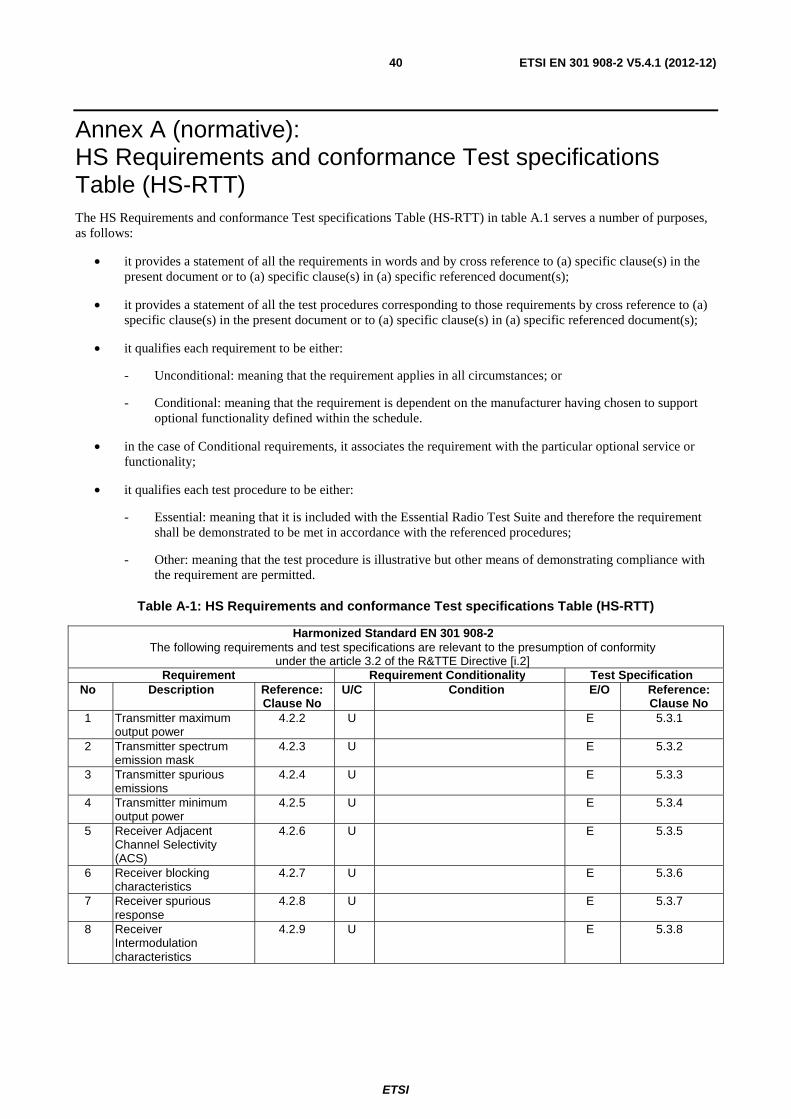
ETSI
ETSI EN 301 908-2 V5.4.1 (2012-12) 40
Annex A (normative): HS Requirements and conformance Test specifications Table (HS-RTT) The HS Requirements and conformance Test specifications Table (HS-RTT) in table A.1 serves a number of purposes, as follows:
• it provides a statement of all the requirements in words and by cross reference to (a) specific clause(s) in the present document or to (a) specific clause(s) in (a) specific referenced document(s);
• it provides a statement of all the test procedures corresponding to those requirements by cross reference to (a) specific clause(s) in the present document or to (a) specific clause(s) in (a) specific referenced document(s);
• it qualifies each requirement to be either:
- Unconditional: meaning that the requirement applies in all circumstances; or
- Conditional: meaning that the requirement is dependent on the manufacturer having chosen to support optional functionality defined within the schedule.
• in the case of Conditional requirements, it associates the requirement with the particular optional service or functionality;
• it qualifies each test procedure to be either:
- Essential: meaning that it is included with the Essential Radio Test Suite and therefore the requirement shall be demonstrated to be met in accordance with the referenced procedures;
- Other: meaning that the test procedure is illustrative but other means of demonstrating compliance with the requirement are permitted.
Table A-1: HS Requirements and conformance Test specifications Table (HS-RTT)
Harmonized Standard EN 301 908-2 The following requirements and test specifications are relevant to the presumption of conformity
under the article 3.2 of the R&TTE Directive [i.2] Requirement Requirement Conditionality Test Specification
No Description Reference: Clause No
U/C Condition E/O Reference: Clause No
1 Transmitter maximum output power
4.2.2 U E 5.3.1
2 Transmitter spectrum emission mask
4.2.3 U E 5.3.2
3 Transmitter spurious emissions
4.2.4 U E 5.3.3
4 Transmitter minimum output power
4.2.5 U E 5.3.4
5 Receiver Adjacent Channel Selectivity (ACS)
4.2.6 U E 5.3.5
6 Receiver blocking characteristics
4.2.7 U E 5.3.6
7 Receiver spurious response
4.2.8 U E 5.3.7
8 Receiver Intermodulation characteristics
4.2.9 U E 5.3.8

ETSI
ETSI EN 301 908-2 V5.4.1 (2012-12) 41
Harmonized Standard EN 301 908-2 The following requirements and test specifications are relevant to the presumption of conformity
under the article 3.2 of the R&TTE Directive [i.2] Requirement Requirement Conditionality Test Specification
No Description Reference: Clause No
U/C Condition E/O Reference: Clause No
9 Receiver spurious emissions
4.2.10 U E 5.3.9
10 Out-of-synchronization handling of output power
4.2.11 U E 5.3.10
11 Transmitter adjacent channel leakage power ratio
4.2.12 U E 5.3.11
Key to columns:
Requirement:
No A unique identifier for one row of the table which may be used to identify a requirement or its test specification.
Description A textual reference to the requirement.
Clause Number Identification of clause(s) defining the requirement in the present document unless another document is referenced explicitly.
Requirement Conditionality:
U/C Indicates whether the requirement is to be unconditionally applicable (U) or is conditional upon the manufacturers claimed functionality of the equipment (C).
Condition Explains the conditions when the requirement shall or shall not be applicable for a technical requirement which is classified "conditional".
Test Specification:
E/O Indicates whether the test specification forms part of the Essential Radio Test Suite (E) or whether it is one of the Other Test Suite (O).
NOTE: All tests whether "E" or "O" are relevant to the requirements. Rows designated "E" collectively make up the Essential Radio Test Suite; those designated "O" make up the Other Test Suite; for those designated "X" there is no test specified corresponding to the requirement. The completion of all tests classified "E" as specified with satisfactory outcomes is a necessary condition for a presumption of conformity. Compliance with requirements associated with tests classified "O" or "X" is a necessary condition for presumption of conformity, although conformance with the requirement may be claimed by an equivalent test or by manufacturer's assertion supported by appropriate entries in the technical construction file.
Clause Number Identification of clause(s) defining the test specification in the present document unless another document is referenced explicitly. Where no test is specified (that is, where the previous field is "X") this field remains blank.

ETSI
ETSI EN 301 908-2 V5.4.1 (2012-12) 42
Annex B (normative): Environmental profile
B.1 General
B.1.1 Introduction This normative annex specifies the environmental profile of the UE.
B.1.2 Temperature The UE should fulfil all the requirements in the full temperature range as given in table B.1.2-1.
Table B.1.2-1: Temperatures
Range Conditions +15 °C to +35 °C For normal conditions (with relative humidity up to 75 %) -10 °C to +55 °C For extreme conditions (see IEC 60068-2-1 [6] and IEC 60068-2-2 [7])
The low and high extreme temperature conditions are denoted as TL (temperature low, -10 °C) and TH (temperature high, +55 °C).
B.1.3 Voltage The UE should fulfil all the requirements in the full voltage range, i.e. the voltage range between the extreme voltages.
The supplier should declare the lower and higher extreme voltages and the approximate shutdown voltage. For the equipment that can be operated from one or more of the power sources listed in table B.1.3-1, the lower extreme voltage should not be higher, and the higher extreme voltage should not be lower than that specified in table B.1.3-1.
Table B.1.3-1: Power sources
Power source Lower extreme voltage
Higher extreme voltage
Normal conditions voltage
AC mains 0,9 × nominal 1,1 × nominal Nominal Regulated lead acid battery 0,9 × nominal 1,3 × nominal 1,1 × nominal Non regulated batteries: Leclanché Lithium Mercury/nickel and cadmium
0,85 × nominal 0,95 × nominal 0,90 × nominal
nominal
1,1 × nominal nominal
nominal
1,1 × nominal nominal
ETSI
ETSI EN 301 908-2 V5.4.1 (2012-12) 43
B.1.4 Test environment Where a normal environment is required then the normal conditions shown in clauses B.1.2 and B.1.3 should be applied.
Where an extreme environment is required then the various combinations of extreme temperatures together with the extreme voltages shown in clauses B.1.2 and B.1.3 should be applied. The combinations are:
• Low extreme Temperature/Low extreme Voltage (TL/VL);
• Low extreme Temperature/High extreme Voltage (TL/VH);
• High extreme Temperature/Low extreme Voltage (TH/VL);
• High extreme Temperature/High extreme Voltage (TH/VH).

ETSI
ETSI EN 301 908-2 V5.4.1 (2012-12) 44
Annex C (informative): Bibliography
• Directive 2004/108/EC of the European Parliament and of the Council of 15 December 2004 on the approximation of the laws of the Member States relating to electromagnetic compatibility and repealing Directive 89/336/EEC (EMC Directive).
• CEPT/ERC/REC 74-01 (Siófok 1998, Nice 1999, Sesimbra 2002, Hradec Kralove 2005, Cardiff 2011): "Unwanted Emissions in the Spurious Domain".
• Directive 2006/95/EC of the European Parliament and of the Council of 12 December 2006 on the harmonisation of the laws of Member States relating to electrical equipment designed for use within certain voltage limits (LV Directive).
• Commission Decision 2008/477/EC of 13 June 2008 on the harmonisation of the 2 500-2 690 MHz frequency band for terrestrial systems capable of providing electronic communications services in the Community.
• Commission Decision 2010/267/EU of 6 May 2010 on harmonised technical conditions of use in the 790-862 MHz frequency band for terrestrial systems capable of providing electronic communications services in the European Union.

ETSI
ETSI EN 301 908-2 V5.4.1 (2012-12) 45
History
Document history
V1.1.1 January 2002 Publication
V2.2.1 October 2003 Publication
V3.2.1 May 2007 Publication
V4.2.1 March 2010 Publication
V5.2.1 July 2011 Publication
V5.3.1 April 2012 Public Enquiry PE 20120818: 2012-04-20 to 2012-08-20
V5.4.0 October 2012 Vote V 20121216: 2012-10-17 to 2012-12-17
V5.4.1 December 2012 Publication