ESA DSP Day 2016
88
ESA DSP Day 2016 Wednesday June 15 th – Thursday June 16 th 2016 Gothenburg, Sweden Workshop Proceedings Ed. R. Trautner, ESA/ESTEC Noordwijk, The Netherlands
Transcript of ESA DSP Day 2016

ESA DSP Day 2016
Wednesday June 15th – Thursday June 16th 2016
Gothenburg, Sweden
Workshop Proceedings
Ed. R. Trautner, ESA/ESTEC Noordwijk, The Netherlands


Table of Contents Session 1: Rad-Hard DSP Chips
3
Scalable Sensor Data Processor: Architecture and Development Status PINTO, Ricardo; BERROJO, Luis; GARCIA, Elena; TRAUTNER, Roland; RAUWERDA, Gerard; SUNESEN, Kim; REDANT, Steven; ANDERSSON, Jan; HABINC, Sandi; LÓPEZ, Jesus
4
RC64: High Performance Rad-Hard Many-core DSP GINOSAR, Ran; AVIELY, Peleg; LANGE, Fredy; ISRAELI, Tsvika
10
Session 2: Test, Verification and Qualification of DSP Chips
18
ESCC Qualification of Space Components - Schemes and New Opportunities MARTINEZ, Fernando
19
Scalable Sensor Data Processor: Testing and Validation PINTO, Ricardo; TRAUTNER, Roland; RAUWERDA, Gerard; REDANT, Steven; SUNESEN, Kim; ANDERSSON, Jan; HABINC, Sandi; LÓPEZ, Jesús; BERROJO-VALERO, Luis-Rafael; MARTIN, Beatriz; PIARETTE, Fernando; SANCHEZ DE ROJAS, Pablo
23
Session 3: COTS based DSP Systems and Boards
28
High Performance COTS based Computer for Regenerative Telecom Payloads NOTEBAERT, Olivier; BARTHE, Lyonel; VANHOVE, Jean-Luc; PRIEUR, Olivier
29
SpaceWire and SpaceFibre Interconnect for High Performance DSPs PARKES, Steve; MCCLEMENTS, Chris; GONZALEZ VILLAFRANCA, Alberto; FERRER, Albert
34
Session 4: DSP Day Reception and Poster Session
39
Characterization and Qualification of Microcontrollers and DSPs in Extreme Temperatures DOLZOME, Flavien
40
Radiation Intelligent Memory Controller IP Core WANG, Pierre-xiao; SELLIER, Charles
46
DVB-S2 Software Defined Radio Modem on the RC64 Many-core DSP AVIELY, Peleg; RADOVSKY, Olga; GINOSAR, Ran
48
1
Session 5: DSP Software and Applications
59
DSP Benchmark Results of the GR740 Rad-Hard Quad-Core LEON4FT JALLE, Javier; HJORTH, Magnus; ANDERSSON, Jan; FOSSATI, Luca; WEIGAND, Roland
60
A Lightweight Operating System for the SSDP LUNTZER, Armin; OTTENSAMER, Roland; KERSCHBAUM, Franz; REIMERS, Christian
63
MacSpace NAGHMOUCHI, Jamin; BISCHOFF, Ole; MICHALIK, Sören; GINOSAR, Ran; BEREKOVIC, Mladen; AVIELI, Peleg; SCHEIBER, Rolf; REIGBER, Andreas; GELLIS, Hagay
68
Space Debris Detection on the HPDP, A Coarse-Grained Reconfigurable Array Architecture for Space SUAREZ, Diego; WEIDENDORFER, Josef; HELFERS, Tim; BRETZ, Daniel; UTZMANN, Jena
71
Session 6: IP Cores, FPGAs, and their Synergies with DSPs
76
Multi-core DSP sub-system IP RAUWERDA, Gerard; SUNESEN, Kim; BRUINTJES, Tom; HOANG THANH, Tung; POTMAN, Jordy
77
DSP and FPGA: Competition, Synergy, and Future Integration in Space ASICs TRAUTNER, Roland; MERODIO CODINACHS, David; WEIGAND, Roland; BOTH, Johannes
81
2
Session 1:
Rad-Hard DSP Chips
3

Scalable Sensor Data Processor: Architecture and Development Status R. Pinto
a , L. Berrojo, E. Garcia, R. Trautner
b, G. Rauwerda
c, K. Sunesen, S. Redant
d, S. Habinc
e,
J. Andersson, J. Lópezf
aThales Alenia Space Spain (TAS-E), 28760 Tres Cantos, Spain
bESA, 2200 AG Noordwijk, The Netherlands
cRecore Systems B.V., 7500 AB Enschede, The Netherlands
dIMEC, B-3001 Leuven, Belgium
eCobham Gaisler AB, SE-411 19 Göteborg, Sweden
fArquimea Ingeniería, S.L.U., 28919 Leganés, Madrid, Spain
Abstract
Future science missions are envisaged to be demanding
w.r.t. on-board data processing capabilities, due to the scarcity
of downlink bandwidth together with the massive amount of
data which can be generated by next-generation instruments,
both in terms of data rate and volume. Therefore, new
architectures for on-board data processing are needed.
The Scalable Sensor Data Processor (SSDP) is a next-
generation mixed-signal ASIC aiming at fulfilling the
processing needs of such missions, integrating in the same
chip a heterogeneous multicore architecture, with two Digital
Signal Processing (DSP) cores and a general purpose
processor, together with Input/Output interfaces and data
acquisition capabilities.
This paper details the current development of the SSDP
ASIC, providing an overview of its architecture and
highlighting the processing capabilities, together with design
enhancements stemming from previous projects. The project
status is also documented, both regarding current and future
activities and milestones.
I. INTRODUCTION
Instruments for future space missions are getting more
capable, offering the possibility of acquiring larger sets of
data, e.g. higher resolution. However, the on-board data
storage and downlink bandwidth are not keeping up with such
capabilities, and are regarded as the bottlenecks for the
exploitation of the instrument. This constraint is not recent,
and many techniques for on-board data processing and
reduction have been introduced in order to overcome it, or at
least mitigate it: decimation, filtering, down-sampling,
compression, among others.
Data processing and reduction algorithms often require
specialized hardware, in order to be implemented in an
efficient way. Such hardware can be Field-Programmable
Gate Arrays (FPGAs) or even Application-Specific Integrated
Circuits (ASICs), which have a non-negligible impact both in
terms of cost and development time. Furthermore, such
processing hardware is usually a companion to control
hardware, which is in charge of instrument/payload control,
together with local house- and time-keeping tasks, processing
and input/output activities.
The Scalable Sensor Data Processor (SSDP) is a next
generation on-board data processing mixed-signal ASIC,
envisaged to be used in future scientific missions requiring
high on-board data processing capabilities, but without
neglecting the control functions. It offers a novel
heterogeneous multicore architecture, combining two high-
performance Xentium Digital Signal Processing (DSP) cores
[1] together with a LEON3FT general-purpose processor
(GPP) [2], all integrated in a System-on-a-Chip (SoC) design
and served by a rich set of Input/Output (I/O) interfaces,
including on-chip Analogue-to-Digital Converters (ADCs).
The envisaged domains of applicability of the SSDP are
future science and robotic exploration missions like JUICE
[3], easing the development and implementation of data
processing functions, without neglecting the control
capabilities offered by a GPP. The main forces driving its
design are processing power, power consumption and
radiation tolerance. The focal point of these characteristics
lies between flexibility and scalability, enabling the usage of
the SSDP in missions with profiles so diverse as deep-space
missions or planetary landers.
The SSDP builds on the experience and expertise gathered
through the successful Massively Parallel Processor
Breadboard (MPPB) project [4] commissioned by ESA,
which aimed at developing a demonstrator of a (scalable)
heterogeneous multicore DSP platform for Space applications.
The mapping into ASIC technology will be performed with
DARE180 digital cells. Development is sustained by a
consortium led by Thales Alenia Space España, and
comprising Recore Systems, IMEC, Cobham Gaisler and
Arquimea, bringing together expertise in the digital, analogue
and mixed-signal domains. Such diverse expertise is of the
utmost importance in order to tackle the technical challenges
posed by integrating the many different components, yet
achieving the proposed goals.
This paper is organized in the following manner: Section
II provides some on-board processing use-cases envisaged for
future Space applications, Section III provides an overview
on the SSDP Architecture, namely its subsystems and I/O
interfaces; Section IV details the processing capabilities of the
SSDP, including architectural enhancements introduced;
Section V presents the current project status and timeline for
the following stages and milestones, and finally Section VI
concludes this paper.
4

II. FUTURE SRE DATA PROCESSING NEEDS
Future data processing needs of Science and Robotic
Exploration (SRE) missions can be divided in two major
domains: on-board data reduction; robotics processing and
control. Each domain has its own specificities regarding
processing needs, briefly presented in this section.
Nevertheless, there is a common denominator in both
domains: processing power, in order to execute sophisticated
algorithms.
A. On-board Data Reduction
Next-generation instruments are capable of generating a
massive amount of data, which can be orders of magnitude
higher than the available down-link. A first form of data
reduction can be achieved by performing digital signal
processing on the captured samples, with (simple) functions
like filtering and down-sampling. Nevertheless, more
sophisticated functions which are currently performed at
ground segment level can be performed directly on-board.
Another form of on-board data reduction can be achieved
by performing compression on the data. Several standards
exist, both for general data and images, and typically resort to
transforms and other algorithms which are suitable to be
implemented by DSPs.
B. Robotics Processing and Control
Robotics is a vast yet growing domain, with several
different disciplines like computer science, algorithms and
mechanics. Current robotics-based missions are highlighting
the need for not only powerful processing capabilities, but
also appropriate I/O interfaces for precise control, including
exploitation of sensors and actuators.
1) Image Processing
A typical application in robotics is image and vision
processing, which requires a fair amount of processing power.
Such processing is used by the robotics application to identify
its surroundings, and then be able to take a decision regarding
its future state based on what it finds.
An illustrative example is path-decision algorithms of a
rover, which requires identifying potential routes – and
hazards – before moving. Such class of algorithms is
processing-intensive due to the amount of data and steps
needed to take a decision. Moreover, they can be time and
energy consuming if the appropriate processing architecture is
not used.
2) Actuator and Drive Control
Another robotics application deals with the control of
actuators, e.g. motors. This kind of applications usually
involves a feedback control loop: gathering information from
sensors, input it into a control algorithm e.g. PID1, and then
use the output to control actuators, like wheel motors or
steering. Such application requires not only processing power
– in fact the requirements for control are usually modest, with
loops below the kHz range - but also a set of special-purpose
input/output interfaces, like general-purpose pins, low-speed
ADCs and pulse-width modulated (PWM) outputs.
1 Proportional, Integral, Derivative
III. SSDP ARCHITECTURE
Most systems nowadays follow the System-on-a-Chip
(SoC) paradigm, embedding in the same package processing
resources together with Input/Output (I/O) interfaces. The
SSDP is not an exception, aiming at providing in a single chip
all the resources needed to perform a wide range of tasks
pertaining to on-board data processing.
The SSDP architecture can be divided in two major
subsystems, based on their main scope:
Control, with a General-Purpose Processor (GPP) at
its heart, providing general control tasks including
Fault Detection, Isolation and Recovery (FDIR)
functions;
Processing, with two Digital Signal Processors
(DSPs) providing the raw processing power together
with high-speed I/O.
A top-level block diagram depicting the two subsystems
and their interconnection is shown in Figure 1.
Figure 1: SSDP High-level Block Diagram
Each subsystem has its own internal SoC bus: AMBA for
Control, a Network-on-a-Chip (NoC) for Processing. The
subsystems are interconnected via a special-purpose Bridge
interface, allowing them to exchange information such as data
and signalling (interrupts and errors). Reception of signalling
information from the Processing subsystem permits the
effective implementation on the Control subsystem of FDIR
handling mechanisms.
The two subsystems have a set of local and networked I/O
interfaces: Controller Area Network (CAN), SpaceWire
(SpW) with RMAP target support, Serial Peripheral Interface
(SPI), Pulse-Width Modulator (PWM), among others, which
gives a high degree of flexibility w.r.t. applications. Dynamic
power saving was not neglected, and a clock gating is used to
turn-off major IP cores when not in use, enabling significant
power savings.
Besides the diverse I/O interface set, the SSDP is also
capable of performing both on- and off-chip data acquisition
and conversion, using Analogue-to-Digital (ADCs), and
Digital-to-Analogue (DAC) converters. On-chip ADCs
provide both high- and low-speed capabilities, allowing a
wide spectrum of applications ranging from high-speed sensor
data acquisition to low-rate house-keeping activities.
5
A. Control Subsystem
At the heart of the Control Subsystem there is a SoC based
on the flight-proven Cobham Gaisler LEON3FT, a fault-
tolerant SPARC V8 architecture. The SoC modules are
interconnected via a shared 32-bit ARM AMBA 2.0 bus,
yielding a maximum throughput of 3.2 Gbps. A block
diagram depicting the Control Subsystem and its components
is shown in Figure 2, with the remaining SoC components,
also from the Cobham Gaisler GRLIB.
Figure 2: SSDP Control Subsystem Block Diagram
The following Sections detail some of the features of the
Control Subsystem depicted in Figure 2.
1) Input/Output Interfaces
The Control Subsystem has a rich set of I/O interfaces,
both local and networked, allowing it to interact with and/or
control both local and remote devices/systems. Such
interfaces range from SpW and CAN to local device control
with SPI or I2C.
There are interfaces dedicated to directly interface with
actuators, such as Pulse-Width Modulation (PWM) outputs.
The provision of such functions in hardware paves the way to
fine-grained control of actuators, such as brushless motors.
Analogue I/O interfaces also exist, such as an on-chip low-
speed current DAC. The purpose of such device is to be able
to measure external temperature via a thermistor such as a
platinum probe (Pt1000). This interface is complemented by a
low-speed voltage ADC, intended primarily to be used in
house-keeping activities, but also capable of being used in
other applications.
2) Memory Support
The storage and execution of software applications is
supported by a Fault-Tolerant Memory Controller supporting
both non-volatile (mature PROM, EEPROM and novel
MRAM) and volatile (SRAM) memory technologies.
Furthermore, these can be protected by Error Detection and
Correction (EDAC) mechanisms in order to ensure reliable
operation in the harsh space environment. These are further
aided by dedicated and autonomous memory scrubbing
hardware mechanisms (not shown in Figure 2).
3) House-keeping and Time-keeping & distribution
As previously mentioned, house-keeping data can be
acquired with the on-chip low-speed ADC. The device is
capable of measuring several parameters, either internal to the
ASIC or external, e.g. internal supply voltage or temperature.
Time-keeping services are also provided, and
complemented by (Spacecraft/Instrument) time distribution is
managed by the novel SpaceWire Time Distribution Protocol
(SpW-TDP) [5], whose IP core has been enhanced with time-
keeping and management functions. Besides the presence of
SpW-TDP, local time distribution and synchronization is also
possible via dedicated input pins, e.g. Pulse Per Second (PPS).
4) Operating System and Debug Support
Operating system (OS) support is provided, via timer
units, interrupt controller and even a Memory Management
Unit (MMU). Such components allow running both Real-
Time Operating Systems (RTOS) like RTEMS, or modern
generic operating systems like Linux.
A Debug Support Unit is provided for on-ground
application development, using standard Cobham Gaisler
tools, together with profiling mechanisms.
5) Advanced Features
Although the LEON3FT GPP is envisaged to be mostly in
charge of SSDP control activities, its processing features were
not neglected, being endowed with advanced features such as:
High-performance IEEE-754 compliant Double
Precision Floating Point Unit (FPU);
Separate 4-way set-associative 16 kB Data and
Instruction cache memories.
Furthermore, it is possible to lock lines of instruction
cache, allowing to speed-up the execution of some portions of
code by reducing latency, e.g. fast interrupt-handling routines.
6) Summary
The Control Subsystem offers many resources which
enable its exploitation as a fully capable On-Board Computer
(OBC) component, without neglecting processing tasks:
Networked I/O: CAN, SpW
Local I/O : GPIO, SPI, I2C, among others
EDAC-protected Memory Storage
Timer Units, IRQ Controller, MMU
House-keeping, Time-keeping and distribution
FPU and Cache Memories
The architecture of the Control Subsystem is intended to
be highly compatible with the commercially available
GR712RC GPP from Cobham Gaisler [6], which is also based
on the LEON3FT. The objective of such compatibility is to
allow the reuse in the SSDP of code, tools and procedures
already developed for the GR712RC and its applications.
6

B. Processing Subsystem
The Processing Subsystem is powered by a multicore SoC
based on the novel Recore Systems’ Xentium Processor [1], a
VLIW2 fixed-point DSP architecture. The DSPs are connected
to the remaining SoC components via a high-performance
Network-on-a-Chip (NoC) interconnect. The SSDP
Processing Subsystem is depicted in Figure 3 through a block
diagram, showing how the SoC components are connected via
the NoC.
Figure 3: SSDP Processing Subsystem Block Diagram
SoC elements are connected via Network Interfaces (NI)
to NoC routers with 32-bit full-duplex links, yielding a
maximum throughput of 3.2 Gbps each way. Each router has
five ports: one for the NI, and four to connect to other
adjacent routers (see Figure 3). The following sections detail
the characteristics of the SoC components.
1) Xentium Processor
The Xentium Processor is a 32-bit fixed-point high-
performance parallel Processing Element (PE) capable of
executing multiple instructions on multiple data (MIMD). The
Xentium Processor is depicted in Figure 4, showing its main
components: Tightly Coupled memory (TCM), providing a
high-bandwidth connection to the NoC for data input/output;
Datapath, with the computing resources used for processing;
Instruction Cache for speeding-up the execution of
application program code..
Figure 4: Xentium Processor
The Datapath is composed by functional units (FUs),
providing the data computing resources, and register files
2 Very-Large Instruction Word
(RFs), providing temporary data storage. There are ten FUs,
which are grouped based on the different operations they can
perform: arithmetic, logical, multiplication and load/store.
Execution can be controlled through external status signals,
e.g. synchronization (wait on bit).
There are five RFs, each with two read and write ports
each, allowing two simultaneous operations. Datapath data
input and output is managed by the load/store FUs, which are
connected via 64-bit ports to the Tightly-Coupled Memory
(TCM), running at system speed and organized in four
independent banks, thus allowing the programmer to design
the application in order to avoid FU contention upon memory
access.
The Xentium Processor is capable of performing the
following operations per clock cycle:
- 4x 16-bit Multiply-Accumulate Operations (MACs)
- 2x 16-bit Complex MACs
- 2x 32-bit MACs
- 2x 64-bit load/store operations
2) Input/Output and Data Acquisition
I/O interfacing was not neglected on this subsystem,
despite having as main scope the processing of massive
amounts of data. Two SpW interfaces with RMAP target are
available to be used directly by the Xentium Processors.
These interfaces are capable of exchanging data with a data
rate up to 200 Mbps.
Data acquisition and conversion is also a feature of the
Processing Subsystem, with both on- and off-chip acquisition
(ADCs). On-chip acquisition is envisaged to be capable of
acquiring 16-bit samples at 100 Mega-samples per second,
(re)using an ADC design developed under previous ESA
contracts. Off-chip acquisition has been designed to interface
with already existing radiation-hardened ADCs. The sample
rate of this interface allows up to 50 Mega-samples per
second acquisitions, with a sample width up to 16-bit.
3) Memory Hierarchy
Efficient exploitation of memory hierarchy is the crux of
effective processing algorithms’ implementations, often the
application’s bottleneck resides in the rate at which data can
be put and retrieved to/from the processing element or system.
The SSDP has a full-fledged memory hierarchy in place,
listed here from high latency to low latency:
High capacity SDRAM Memory, up to 512 MB
Internal low-latency 64 kB SRAM Memory Tile
Local TCMs, 32 kB per Xentium Processor
The Memory Tile provides a large SRAM accessible via
the NoC at full system speed, which can be used to store large
chunks of data which will then be transferred either to the
TCMs, SDRAM or any available I/O interface. This allows
the implementation of a software-based cache memory.
Memory addressing is performed in little-endian, i.e. the least
significant byte is stored in the lowest address.
7
4) System Scaling
The scaling of SSDP-based systems has been envisaged,
and with that purpose a Chip-to-Chip (CtC) interface has been
introduced. This full-duplex parallel interface has a 16-bit
width, and is capable of exchanging data at a speed up to 50
MWords per second, yielding a maximum throughput of 800
Mbps. The interface has hardware-based flow-control
mechanisms, thus enabling reliable communication support.
The CtC interface allows data exchange between one or more
SSDP devices, or the exploitation of companion devices,
including functions supported by FPGAs (see Figure 5).
Figure 5: Chip-to-Chip Interface Usage Examples
The bi-directional interconnection of the SSDP with a
companion FPGA is depicted in Figure 5a, in a star topology:
the FPGA is at the centre, and can be used with a specific
purpose (companion device), and/or be used to route data
between the SSDP devices. A single-device topology would
be a star with a single SSDP. Another topology is shown in
Figure 5b, where the devices are connected in a ring topology.
These topologies enable a powerful processing chain, with
each device being in charge of a given task, or subset of tasks,
or even being connected to multiple different
instruments/acquisition devices.
5) Summary
The Processing Subsystem provides a high-performance
multicore DSP SoC, with data acquisition capabilities. Its
most striking features are:
Multicore 32-bit fixed-point VLIW DSP (x2)
Internal 64 kB SRAM, external SDRAM
SpW I/F with RMAP target, up to 200 Mbps (2x)
On-chip ADC up to 100 Msps
Off-chip ADC and DAC up to 50 Msps
Chip-to-Chip Interface, up to 800 Mbps
These features can be efficiently exploited by application
designers through compilers and a graphical Software
Development Environment, with debugging capabilities.
IV. SSDP ADVANCED FEATURES
The SSDP draws heavily from the MPPB platform,
inheriting most of its architecture and components. Building
on this heritage, improvements and features were introduced,
based on MPPB usage and evaluation activities performed
both by industry and academia. This section details some of
the advanced features, and how they can enable the design
and implementation of sophisticated systems and algorithms.
A. Efficient DMA Transfers
The availability of DMA transfers allows the exchange of
data autonomously, without needing processor intervention.
The SSDP Processing Subsystem provides a DMA Controller
which is capable of performing stride-based transfers, where
data which is not stored in contiguous positions can still be
efficiently accessed without paying a severe penalty. The
same feature can be used for sub-sampling / decimation
without consuming processor/DSP resources.
The availability of DMA transfers (both 2D and stride-
based) enables creative – and efficient - uses of the memory
hierarchy. An example is implementing an effective software-
based cache, with the DMA controller being used to transfer
data between the SDRAM, Memory Tile and TCMs, for
ensuring that the Xentium processors would always be
working on data, i.e. they would not suffer data starvation.
B. Endianness Conversion
Memory accesses performed by most of Processing
Subsystem modules are done in little endian, i.e. the least-
significant byte is stored at the lowest memory address. Such
access fashion clashes with the one used by the Control
Subsystem, whose modules inherit the big-endian addressing
from the LEON3FT architecture.
The issue of endianness conversion is addressed on the
SSDP at the points where information has to cross a so-called
“endianness domain crossing”, i.e the bridges between the
two subsystems. At these points there are specially crafted
mechanisms to provide automatic and transparent conversion.
Transparency is achieved by having different memory maps
for big- and little-endian information exchange, which will
determine if there should be a conversion or not.
C. Application Profiling
Profiling an application is the logical step to be taken after
its (initial) implementation and validation, and it should be
performed before attempting to introduce any optimization.
The Xentium Processors have been enhanced w.r.t. profiling
support, with new performance monitoring mechanisms
added. A new set of counters is provided, which can be used
to assess the performance of an application in a non-intrusive
manner: read and write cycles, latency, cache misses and hits,
among others.
D. Fault Detection, Isolation and Recoveryl
Space-based applications must provide FDIR functions in
order to be able to cope with errors induced by the harshness
of the Space environment. Such function must be built on top
of hardware-based mechanisms, providing the capability of
detecting errors, which may trigger faults.
In the SSDP the Control Subsystem is in charge of dealing
with FDIR functions. In order to provide effective FDIR, the
NoC and modules of the Processing Subsystem have been
enhanced w.r.t. error detection and signalling capabilities.
Such capabilities allow the hardware based detection of
errors. Error notifications are forwarded to the Control
Subsystem in order to trigger the execution of appropriate
handlers.
(a) Star/Single
(b) Ring
8

V. DEVELOPMENT & STATUS
The SSDP is being developed through an industrial
consortium led by Thales Alenia Space España (ES), and
encompassing several partners across Europe with different
domains of expertise:
Recore Systems (NL), providing the multicore DSP
and components of the Processing Subsystem,
together with the Software Development Environment
(SDE) and support;
Cobham Gaisler (SE), with the LEON3FT SoC and
support
IMEC (BE), providing specific IP cores, DARE180
cell library, and also the layout services, package,
assembly support, foundry interface and manufacture
testing;
Arquimea (ES), with the on-chip fast ADC.
The SSDP is now at its development and validation stage,
including FPGA-based prototyping. The SSDP development
will result in a CQFP-352 mixed-signal ASIC, built in UMC
180 nm technology with DARE180 digital cell technology
[6]. Engineering Models (EMs), Flight Models (FMs) and
evaluation boards will be commercialized by Cobham Gaisler.
A. Prototyping, Testing and Validation
The prototyping and testing activities are being carried out
on a custom board based on a Xilinx Kintex Ultrascale FPGA,
providing enough resources to accommodate both SSDP
subsystems. The schematic was captured internally at TAS-E,
and the manufacture commissioned to Pender Electronics.
This board will provide all the I/O interfaces needed by the
SSDP, thus allowing their validation.
The SSDP testing and validation activities are being
carried out with support of a National Instruments PXI
testbench comprising both hardware and LabView software.
The SSDP runs small pieces of software to support the
validation procedures. Such a setup allows a simple yet
powerful validation loop, which can be used at all levels of
the validation procedures, from interfaces to full system.
Benchmarking will be performed throughout the
development cycle, in order to characterize the SSDP from a
processing point of view. For that purpose, the NGDSP
benchmark suite [8] will be used.
B. Development Milestones
The SRR was successfully closed out in October 2015,
and the current activities related to development and
subsystem integration will culminate with a PDR in 2016. The
current schedule for the following (major) milestones is the
following:
Q1 2017 – CDR
Q2 2017 – Prototypes Manufacturing
Q3/Q4 2017 – Prototypes (EM) Available
2018 – FM Available
Evaluation boards with EMs are expected also during
Q3/Q4 2017, after the testing and validation campaign.
VI. CONCLUSIONS
The Scalable Sensor Data Processor (SSDP) is a next-
generation data processing mixed-signal ASIC, providing in a
single package a sophisticated architecture with a Processing
Subsystem with powerful multicore DSP processing
capabilities, together will a Control Subsystem using well-
established general-purpose processing resources capable of
delivering fast and reliable control and house-keeping. Each
of these is a full System-on-a-Chip (SoC) on its own, with
Input/Output capabilities besides the processing resources.
The Control Subsystem offers a general-purpose
LEON3FT with a floating-point unit, together with
SpaceWire, CAN and local I/O such as SPI and I2C, being
highly compliant with the LEON3FT-based Cobham Gaisler
GR712RC SoC, thus allowing the porting to the SSDP of
applications developed for such platform.
Besides the powerful Xentium Processors, the Processing
Subsystem is supported by a high-performance Network-on-
Chip (NoC), interconnecting the processing resources,
SDRAM storage, I/O such as SpW and on- and off-chip data
acquisition for ADCs and DACs. A Chip-to-Chip interface is
also provided, allowing scaling a system with other devices,
such as additional SSDP ASICs, FPGAs or others.
The SSDP RTL is currently being integrated, tested and
validated, supported by a custom FPGA-based prototyping
board. The next step after validation will be to perform the
ASIC layout. The SSDP ASIC will be implemented in UMC
180 nm technology, using DARE180 digital cells, providing a
high degree of SEE tolerance which is in line with envisaged
future science and robotic exploration missions. The first
prototypes for testing and validation are expected to be
delivered during the second half of 2017, with evaluation
boards being made available by Cobham Gaisler.
VII. REFERENCES
[1] Recore Systems, “Xentium® VLIW DSP IP Core - Product
Brief,” 2012. [Online]. Available:
http://www.recoresystems.com/fileadmin/downloads/Product_br
iefs/2012-2.0_Xentium_Product_Brief.pdf.
[2] Cobham Gaisler, “GRLIB IP Core User's Manual,” April 2016.
[Online]. Available:
http://www.gaisler.com/products/grlib/grlib.pdf.
[3] European Space Agency, “JUICE Definition Study Report,”
2014.
[4] Recore Systems, “Massively Parallel Processor Breadboarding
Study,” 2012.
[5] Cobham Gaisler, “High Accuracy Time Synchronization over
SpaceWire Networks,” 2013.
[6] Cobham Gaisler, GR712RC Dual-Core LEON3-FT SPARC V8
Processor, 2016.
[7] S. Redant, R. Marec, L. Baguena, E. Liegeon, J. Soucarre, B.
Van Thielen, G. Beeckman, P. Ribeiro, A. Fernandez-Leon and
B. Glass, “The Design Against Radiation Effects (DARE)
Library,” in 5th Radiation Effects on Components and Systems
Workshop (RADECS), Madrid, 2004.
[8] TEC-EDP/2008.18/RT, “Next Generation Space Digital Signal
Processor Software Benchmark,” ESA, 2008.
9

RC64: High Performance Rad-Hard Manycore
Ran Ginosar, Peleg Aviely, Fredy Lange and Tsvika Israeli
Ramon Chips, Ltd., 5 HaCarmel Street, Yoqneam Illit 2069201, Israel
[ran, peleg, fredy, tsvika]@ramon-chips.com
Abstract
RC64 is a rad-hard manycore DSP combining 64
VLIW/SIMD DSP cores, lock-free shared memory, a
hardware scheduler and a task-based programming model.
The hardware scheduler enables fast scheduling and
allocation of fine grain tasks to all cores.
I. INTRODUCTION
Multiple core architectures are divided into multi-cores and
many-cores. Multi-cores, ranging from rad-hard Gaisler/
Ramon Chips’ LEON3FT dual-core GR712RC to
commercial ARM Cortex A9 and Intel Xeon, typically
provide some form of cache coherency and are designed to
execute many unrelated processes, governed by an operating
system such as Linux. In contrast, many-cores such as Tilera
TilePro, Adapteva’s Epiphany, NVidia GPU, Intel Xeon Phi
and Ramon Chips’ RC64, execute parallel programs
specifically designed for them and avoid operating systems,
in order to achieve higher performance and higher power-
efficiency.
Many-core architectures come in different flavors: a two-
dimensional array of cores arranged around a mesh NoC
(Tilera and Adapteva), GPUs and other manycores with
clusters of cores (Kalray), and rings. This paper discusses
the Plural architecture [12]—[16] of RC64 [17], in which
many cores are interconnected to a many-port shared
memory rather than to each other (Figure 1).
Many cores also differ on their programming models,
ranging from PRAM-like shared memory through CSP-like
message-passing to dataflow. Memory access and message
passing also relate to data dependencies and
synchronization—locks, bulk-synchronous patterns and
rendezvous. RC64 architecture employs a strict shared
memory programming model.
The last defining issue relates to task scheduling—allocating
tasks to cores and handling task dependencies. Scheduling
methods include static (compile time) scheduling, dynamic
software scheduling, architecture-specific scheduling (e.g.,
for NoC), and hardware schedulers, as in RC64, in which
data dependencies are replaced by task dependencies in
order to enhance performance and efficiency and to simplify
programming.
As a processor designed for operation in harsh space
environment, RC64 is based on rad-hard technology and
includes several mechanisms to enhance its fault tolerance,
such as EDAC, and to handle fault detection, isolation and
recovery (FDIR).
Figure 1. RC64 Many-Core Architecture. 64 DSP cores,
modem accelerators and multiple DMA controllers of I/O
interfaces access the multibank shared memory through a
logarithmic network. The hardware scheduler dispatches fine
grain tasks to cores, accelerators and I/O.
10
II. RELATED WORK
GR712RC, an early dual-core rad-hard space processor was
introduced by Ramon Chips and Cobham Gaisler [1][2].
Other multi-core architectures, not intended for space,
include ARM Cortex A9 [3] and Intel Xeon. Many core
architectures include the mesh-tiled Tilera [4][5] and
Adapteva [6], NVidia GPU [7], Intel ring-topology Xeon
Phi [8] and dataflow clusters by Kalray [9]. The research
XMT manycore [10] is PRAM-inspired and employs
hardware scheduling, similar to RC64. It employs
declarative parallelism to direct scheduling [11]. The Plural
architecture and its RC64 incarnation are discussed
in [12]—[17] and is the subject of the MacSpace European
FP7 research project [18]. An early hardware scheduler is
reported in [19]. The baseline multistage interconnection
network has been introduced in [20]. Example of SDR
modem implementation on RC64 and simulated
performance results are given in [26].
Other efforts to introduce rad-hard manycores for space
include the FPGA-based AppSTAR at Harris [22], Maestro
at Boeing [23] and RADSPEED at BAE Systems [24].
III. RC64 ARCHITECTURE
This section presents the Plural architecture of RC64
(Figure 1). RC64 architecture defines a shared-memory
single-chip many-core. The many-core consists of a
hardware synchronization and scheduling unit, 64 DSP
cores, and a shared on-chip memory accessible through a
high-performance logarithmic interconnection network. The
cores contain instruction and data caches, as well as a
private ‘scratchpad’ memory. The data cache is flushed and
invalidated by the end of each task execution, guaranteeing
consistency of the shared memory. The cores are designed
for low power operation using ‘slow clock’ (typically
slower than 500 MHz). Performance is achieved by high
level of parallelism rather than by sheer speed, and access to
the on-chip shared memory across the chip takes only a
small number of cycles.
The on-chip shared memory is organized in a large number
of banks, to enable many ports that can be accessed in
parallel by the many cores, via the network. To reduce
collisions, addresses are interleaved over the banks. The
cores are connected to the memory banks by a multi-stage
many-to-many interconnection network. The network
detects access conflicts contending on the same memory
bank, proceeds serving one of the requests and notifies the
other cores to retry their access. The cores immediately retry
a failed access. Two or more concurrent read requests from
the same address are served by a single read operation and a
multicast of the same value to all requesting cores. As
explained in the next section, there is no need for any cache
coherency mechanism.
The CEVA X1643 DSP core comprises the following parts.
The computation unit consists of four multiplier-
accumulators (MAC) of 16-bit fixed point data, supporting
other precisions as well, and a register file. Ramon Chips
has added a floating point MAC. The data addressing units
includes two load-store modules and address calculation.
The data memory unit consists of the data cache, AXI bus
interface, write buffers for queuing write-through
transactions and a scratchpad private memory. The program
memory unit is the instruction cache. Other units support
emulation and debug and mange power gating. Thus, the
DSP core contains three memories: an instruction cache, a
write-through data cache and a scratchpad private memory.
Implemented in 65nm CMOS and designed for operation at
300 MHz, RC64 is planned to achieve 38 GFLOPS (single
precision) and 76 GMAC (16-bit). With 12 high speed serial
links operating at up to 5 Gbps in each direction, a total
bandwidth of 120 Gbps is provided. Additional high
bandwidth is enabled for memories (25 Gbps DDR3
interface of 32 bit at 800 Mword/s with additional 16 bits
for ECC) and for high performance ADC and DAC (38
Gbps over 48 LVDS channels of 800 Mbps). The device is
planned to dissipate less than 10 Watt in either CCGA or
PBGA 624 column or ball grid array packages.
IV. RC64 PROGRAMMING MODEL
The Plural PRAM-like programming model of RC64 is
based on non-preemptive execution of multiple sequential
tasks. The programmer defines the tasks, as well as their
dependencies and priorities which are specified by a
(directed) task graph. Tasks are executed by cores and the
task graph is ‘executed’ by the scheduler.
In the Plural shared-memory programming model,
concurrent tasks cannot communicate. A group of tasks that
are allowed to execute in parallel may share read-only data
but they cannot share data that is written by any one of
them. If one task must write into a shared data variable and
another task must read that data, then they are dependent—
the writing task must complete before the reading task may
commence. That dependency is specified as a directed edge
in the task graph, and enforced by the hardware scheduler.
Tasks that do not write-share data are defined as
independent, and may execute concurrently. Concurrent
execution does not necessarily happens at the same time—
concurrent tasks may execute together or at any order, as
determined by the scheduler.
Some tasks, typically amenable to independent data
parallelism, may be duplicable, accompanied by a quota
that determines the number of instances that should be
executed (declared parallelism [11]). All instances of the
same duplicable task are mutually independent (they do not
write-share any data) and concurrent, and hence they may
be executed in parallel or in any arbitrary order. These
instances are distinguishable from each other merely by
their instance number. Ideally, their execution time is short
(fine granularity). Concurrent instances can be scheduled for
11
execution at any (arbitrary) order, and no priority is
associated with instances.
Each task progresses through at most four states (Figure 2).
Tasks without predecessors (enabled at the beginning of
program execution) start in the ready state. Tasks that
depend on predecessor tasks start in the pending state. Once
all predecessors to a task have completed, the task becomes
ready and the scheduler may schedule its instances for
execution and allocate (dispatch) the instances to cores.
Once all instances of a task have been allocated, the task is
All allocated. And once all its instances have terminated, the
task moves into the terminated state (possibly enabling
successor tasks to become ready).
TerminatedAll
AllocatedReadyPending
Figure 2. Task State Graph
Many-flow pipelining facilitates enhanced core utilization in
streamed signal processing. Consider the task graph
examples for executing JPEG2000 image compression and
the processor utilization charts of Figure 3. In (a), five tasks
A-E are scheduled in sequence. Tasks B and D are
duplicable with a large number of instances, enabling
efficient utilization of 64 cores. Tasks A,C,E, on the other
hand, are sequential. Execution time of compressing one
image is 160 time units, and overall utilization, reflected by
the ratio of colored area to the 64×160 rectangle, is 65%.
The core utilization chart (on the right) indicates the number
of busy cores over time, and different colors represent
different tasks. In the many-flow task graph (Figure 3b), a
pipeline of seven images is processed. During one iteration,
say iteration k, the output stage sends compressed image k,
task E processes image k+1, task D computes the data of
image k+2, and so on. Notice that the sequential tasks A,C,E
are allocated first in each iteration, and duplicable instances
occupy the remaining cores. A single iteration takes 95 time
units and the latency of a single image is extended to five
iterations, but the throughput is enhanced and the core
utilization chart now demonstrates 99% core utilization.
Data dependencies are expressed (by the programmer) as
task dependencies. For instance, if a variable is written by
task tw and must later be read, then reading must occur in a
group of tasks {tr} and tw{tr}. The synchronization action
of completion of tw prior to any execution of tasks {tr}
provides the needed barrier.
Figure 3. Many-flow pipelining: (a) task graph and single
execution of an image compression program, (b) many-flow task
graph and its pipelined execution
V. RC64 HARDWARE SCHEDULER
The hardware scheduler assigns tasks to cores for execution.
The scheduler maintains two data structures, one for
managing cores (Figure 4) and the other for managing tasks
(Figure 5). Core and task state graphs are shown in Figure 6
and Figure 2, respectively.
The hardware scheduler operates as follows. At start, all
cores are listed as Idle and the task graph is loaded into the
first three columns of the Task Management Table. The
scheduler loops forever over its computation cycle. On each
cycle, the scheduler performs two activities: allocating tasks
for execution, and handling task completions.
Core # State Task # Instance # … …
0
1
2
…
Figure 4. Core Management Table
12

Task # Duplication
quota Dependencies State
#
allocated
instances
#
terminated
instances
0
1
2
…
data from task graph
Figure 5. Task Management Table
BusyIdle
Figure 6. Core State Graph
To allocate tasks, the scheduler first selects ready tasks from
the Task Management Table. It allocates each such task to
idle cores by changing the task state to All Allocated (if the
task is regular, or if all duplicable instances have been
dispatched), by increasing the count of allocated instances in
the Task Management Table, and by noting the task number
(and instance number, for duplicable tasks) in the Core
Management Table. Finally, task/instance activation
messages are dispatched to the relevant cores. The
activation message for a specific core includes the code
entry address and (in case of a duplicable instance) the
instance ID number.
To handle task completions, the scheduler collects
termination messages from cores that have completed task
executions. It changes the state of those cores to Idle. For
regular tasks, the task state is changed to Terminated. For
duplicable tasks, the counter of terminated tasks in the Task
Management Table is incremented, and if it has reached the
quota value then the state of that task is changed to
Terminated. Next, the scheduler updates the Dependencies
entry of each task in the table which depends on the
terminated task: the arrival of that token is noted, the
dependency condition is recomputed, and if all precedencies
of any task have been fulfilled then the state of that task is
changed to Ready, enabling allocation and dispatch in
subsequent scheduler computation cycles.
The scheduler capacity, namely the number of simultaneous
tasks which the scheduler is able to allocate or terminate
during each computation cycle, is limited. Any additional
task allocations and task termination messages beyond
scheduler capacity wait for subsequent cycles in order to be
processed. A core remains idle from the time it issues a
termination message until the next task allocation arrives.
That idle time comprises not only the delay at the scheduler
(wait and processing times) but also any transmission
latency of the termination and allocation messages over the
scheduler-to-cores network.
The allocation and termination algorithms are shown in
Figure 7.
Scheduling efficiency depends on the ratio of scheduling
latency (reflected in idle time of cores) to task execution
time. Extremely fine grain tasks (e.g., those executing for
1~100 cycles) call for very short scheduling latencies (down
to zero cycles) to be efficient. Alternatively, speculative
advanced scheduling may fill queues attached to each core
so that the core can start executing a new instance once it
has completed a previous instance (see [16] for such an
analysis). However, typical tasks tend to incur compiled
overhead (prologue and epilogue code sequences generated
by even the most efficient optimizing compilers), and
typical programming practices of parallel tasks tend to avoid
the shortest tasks, resulting in average task duration
exceeding 100 cycles. With average scheduling latency of
only 10-20 cycles, enabled by hardware implementation, we
obtain execution efficiency close to 99%.
The hardware scheduler is implemented as custom logic in
RC64. Two other possibilities will be considered in future
generations, one based on two content-addressable memory
(CAM) arrays implementing the two management tables,
and another implementation as software executing on a
dedicated fast core with its dedicated high throughput
memory.
Figure 7. Allocation (top) and termination (bottom) algorithms
ALLOCATION
1. Choose a Ready task (according to priority, if
specified)
2. While there is still enough scheduler capacity and
there are still Idle cores
a. Identify an Idle core
b. Allocate an instance to that core
c. Increase counter of allocated task
instances
d. If # allocated instances == quota, change
task state to All Allocated and continue to
next task (step 1)
e. Else, continue to next instance of same
task (step 2)
TERMINATION
1. Choose a core which has sent a termination
message
2. While there is still enough scheduler capacity
a. Change core state to Idle
b. Increment # terminated instances
c. If # terminated instances == quota, change
task state to Terminated
d. Recompute dependencies for all other
tasks that depend on the terminated task,
and where relevant change their state to
Ready
13

A special section of the scheduler schedules High Priority
Tasks (HPTs), which are designed as ‘interrupt handling
routines’ to handle hardware interrupts. As explained in
Section VII, all I/O interfaces (including interfaces to
accelerators) are based on DMA controllers that issue
interrupts once completing their action. The most urgent
portion of handling the interrupt is packaged as a HPT, and
less urgent parts are formulated as a normal task. HPT is
dispatched immediately and pre-emptively by the scheduler.
Each core may execute one HPT, and one HPT does not
pre-empt another HPT. Thus, a maximum of 64 HPTs may
execute simultaneously. RC64 defines fewer than 64
different HPTs, and thus there is no shortage of processors
for prompt invocation of HPTs.
VI. RC64 NETWORKS ON CHIP
RC64 contains two specialized Networks on Chip (NOCs),
one connecting the scheduler to all cores and other
schedulable entities (DMA controllers and accelerators), and
a second NOC connecting all cores and other data sources
(DMA controllers) to the shared memory.
A. Scheduler NOC
The scheduler-to-cores NOC employs a tree topology. That
NOC off-loads two distributed functions from the scheduler,
task allocation and task termination.
The distributed task allocation function receives clustered
task allocation messages from the scheduler. In particular, a
task allocation message related to a duplicable task specifies
the task entry address and a range of instance numbers that
should be dispatched. The NOC partitions such a clustered
message into new messages specifying the same task entry
address and sub-range of instance numbers, so that the sub-
ranges of any two new messages are mutually exclusive and
the union of all new messages covers the same range of
instance numbers as the original message. The NOC nodes
maintain Core and Task Management Tables which are
subsets of those tables in the scheduler (Figure 4 and Figure
5, respectively), to enable making these distributed
decisions.
The distributed task termination process complements task
allocations. Upon receiving instance terminations from
cores or subordinate nodes, a NOC node combine the
messages and forwards a more succinct message specifying
ranges of completed tasks.
B. Shared Memory NOC
The larger NOC of RC64 connects 64 cores, tens of DMA
controllers and hardware accelerators to 256 banks of the
shared memory. To simplify layout, floor-planning and
routing, we employ a Baseline logarithmic-depth multistage
interconnection network [20], symbolically drawn in Figure
1. Some of the NOC switch stages are combinational, while
others employ registers and operate in a pipeline. Two
separate networks are used, one for reading and another one
for writing. The read networks accesses and transfers 16
bytes (128 bits) in parallel, matching cache line size and
serving cache fetch in a single operation. The write network
is limited to 32 bits, compatible with the write-through
mechanism employed in the DSP cores. Writing smaller
formats (16 and 8 bits) is also allowed.
VII. RC64 ACCELERATORS AND I/O
Certain operations cannot be performed efficiently on
programmable cores. Typical examples require bit level
manipulations that are not provided for by the instruction
set, such as used for error correction (LDPC, Turbo code,
BCH, etc.) and for encryption. RC64 offers two solutions.
First, several accelerators for pre-determined computations
(such as LDPC and Turbo Coding, useful in DVB-S2 and
DVB-RCS for space telecommunications) are included on
chip. They are accessible only through shared memory, as
follows. First, the data to be processed by the accelerator are
deposited in shared memory. Next, the accelerator is
invoked. Data is fetched to the accelerator by a dedicated
DMA controller, and the outcome is sent back to shared
memory by a complementing second DMA controller. This
mode of operation decouples the accelerator from the cores
and eliminates busy waiting of cores.
The second possibility is to employ an external acceleration
on either an FPGA or an ASIC. High speed serial links on
RC64 enable efficient utilization of such external
acceleration. This mode offers scalability and extendibility
to RC64.
All input / output interfaces operate asynchronously to the
cores. Each interface is managed by one DMA controller for
input and a second DMA controller for output. Many
different types of I/O interfaces are available in RC64,
including slow GPIO and SpaceWire links, high rate
DDR2/DDR3 and ONFI flash EDAC memory interfaces
(error detection and correction is carried out at the I/O
interfaces, offloading that compute load from the cores),
high speed serial links (implementing SpaceFibre [25],
serial Rapid IO and proprietary protocols) and 48-link
LVDS port useful for ADCs, DACs and other custom
interfaces.
All DMA controllers are scheduled by the scheduler, submit
interrupt signals to the scheduler (as explained in Section V
above), and read and write data directly to the shared
memory through the NOC (see Section VI above). The
system software required for managing I/O is described in
Section VIII below.
VIII. RC64 SYSTEM SOFTWARE
The system run-time software stack is shown schematically
in Figure 8. The boot sequence library is based on the boot
code of the DSP core. It is modified to enable execution by
many cores in parallel. Only one of the cores performs the
shared memory content initialization. The boot code
14

includes DSP core self-test, cache clearing, memory
protection configuration and execution status notification to
an external controlling host.
The Runtime Kernel (RTK) performs the scheduling
function for the DSP core. It interacts with the hardware
scheduler, receives task allocation details, launches the task
code and responds with task termination when the task is
finished. The RTK also initiates the power down sequence
when no task is received for execution.
The first task allocated by the scheduler is responsible for
loading the application task graph into the scheduler. This
code is automatically generated during a pre-compile stage
according to the task graph definition. Application tasks are
allocated after the initialization task is finished.
Certain library routines manage EDAC for memories,
encapsulate messaging and routing services to off-chip
networking (especially over high speed serial SpaceFibre
links), respond to commands received from an external host
(or one of the on-chip cores, playing the role of a host),
perform FDIR functions, and offer some level of
virtualization when multiple RC64 chips are employed in
concert to execute coordinated missions.
Figure 8. RC64 Run Time Software. The kernel enables boot,
initialization, task processing and I/O. Other services include
execution of host commands, networking and routing, error
correction and management of applications distributed over
multiple RC64 chips
Other components of the RTK manage I/O and accelerators.
Configuring the interfaces requires special sequences such
as link detection and activation, clock enabling, DMA
configuration, etc. Each interface has its own set of
parameters according to the required connectivity, storage
type, data rate and so on.
Figure 9 demonstrate the hardware-kernel-application
sequence of events in the case of an input of a predefined
data unit over a stream input link. The DMA controller,
previously scheduled, stores input data into a pre-allocated
buffer in memory (step 1). Upon completion, it issues an
interrupt (step 2). A HPT is invoked (step 3, see Section V)
and stores pointers and status in shared memory, effectively
enqueuing the new arrival (step 4). It ends up by issuing a
‘software event’ to the scheduler (step 5). Eventually, the
scheduler dispatches a task that has been waiting for that
event (step 6). That task can consume the data and then
dequeue it, releasing the storage where the data was stored
(step 7). Other I/O operations are conducted similarly.
Figure 9. Event sequence performing stream input
IX. RC64 SOFTWARE DEVELOPMENT TOOLS
RC64 SDK enables software development, debug and
tuning, as shown in Figure 10. The IDE tool chain includes
a C/C++ compiler for the DSP core, an assembler, a linker,
and a library of DSP functions customized for the core,
taking full advantage of its VLIW capability (computing
and moving data at the same time) and SIMD (performing
several multiply and accumulate operations in parallel).
RC64 Parallel programming is supported by the task
compiler, which translates the task graph for the scheduler, a
many-task emulator (MTE) that enables efficient
development of parallel codes on personal computers, and a
many-core debugger, which synchronizes debug operations
of all cores. The RC64 parallel simulator is cycle accurate,
fully simulating the cores as well as all other hardware
components on the chip.
The profiler provides complete record of parallel execution
on all 64 cores. The event recorder generates traces with
time stamps of desired events. The kernel and libraries are
described in Section VIII above.
15
X. RC64 RADIATION HARDNESS AND FDIR
RC64 will be implemented in 65nm CMOS using
RadSafe™ rad-hard-by-design (RHBD) technology and
library [21]. RadSafe™ is designed for a wide range of
space missions, enabling TID tolerance to 300 kRad(Si), no
latchup and very low SEU rate. All memories on chip are
protected by various means and varying levels of error
correction and detection. Special protection is designed for
registers that hold data for extended time, such as
configuration registers. The two external memory interfaces,
to DDR2/DDR3 and to ONFI flash memories, implement
several types of EDAC. For instance, ten flash memory
chips can be connected for eight byte wide datapath and two
flash devices for storing Reed Solomon ECC.
Figure 10. RC64 Software Development Kit.
RC64 implements extensive means for fault detection,
isolation and recovery (FDIR). An external host can reset,
boot and scrub the device through dual RMAP SpaceWire
ports. RC64 contains numerous error counters and monitors
that collect and report error statistics. Trace buffers,
allocated in shared memory as desired, enable rollback and
analysis (in addition to helping debug). Faulty sub-systems
may be shut down and the scheduler is designed to operate
with partial configurations.
XI. CONCLUSIONS
RC64 is a many core architecture suitable for use in space.
It is designed for simplified PRAM-like shared memory
programming and high performance at low power. RC64
goal is to enable future software-defined satellites in all
space endeavors. RC64 is presently under design and all
performance figures reported herein and in [26] are based on
simulations. RC64 is planned for availability before the end
of the decade. RC64 R&D project is funded by Israel Space
Agency and by the European Union.
XII. ACKNOWLEDGEMENTS
The financial support of the Israel Space Agency, the Israel
Ministry of Defense, the Israel Aerospace Industry and the
European Union (Seventh Framework Programme grant
agreement 607212) is greatly appreciated. Itai Avron has
contributed to early versions of this paper.
XIII. REFERENCES
[1] Sturesson, F., J. Gaisler, R. Ginosar, and T. Liran. "Radiation
characterization of a dual core LEON3-FT processor." In
Radiation and Its Effects on Components and Systems
(RADECS), 2011 12th European Conference on, pp. 938-944.
IEEE, 2011.
[2] Habinc, S., K. Glembo, and J. Gaisler. "GR712RC-The Dual-
Core LEON3FT System-on-Chip Avionics Solution." In
DASIA 2010 Data Systems In Aerospace, vol. 682, p. 8.
2010.
[3] Jacquet, David, Frederic Hasbani, Philippe Flatresse, Richard
Wilson, Franck Arnaud, Giorgio Cesana, Thierry Di Gilio et
al. "A 3 GHz dual core processor ARM cortex TM-A9 in 28
nm UTBB FD-SOI CMOS with ultra-wide voltage range and
energy efficiency optimization." Solid-State Circuits, IEEE
Journal of 49, no. 4 (2014): 812-826.
[4] Villalpando, Carlos Y., Andrew E. Johnson, Raphael Some,
Jacob Oberlin, and Steven Goldberg. "Investigation of the
tilera processor for real time hazard detection and avoidance
on the altair lunar lander." In Aerospace Conference, 2010
IEEE, pp. 1-9. IEEE, 2010.
[5] Wentzlaff, David, et al. "On-chip interconnection architecture
of the tile processor." IEEE micro 5 (2007): 15-31.
[6] Varghese, Anitha, Ben Edwards, Gaurav Mitra, and Alistair
P. Rendell. "Programming the Adapteva Epiphany 64-core
Network-on-chip Coprocessor." In Parallel & Distributed
Processing Symposium Workshops (IPDPSW), 2014 IEEE
International, pp. 984-992. IEEE, 2014.
[7] Nickolls, John, and William J. Dally. "The GPU computing
era." IEEE micro 2 (2010): 56-69.
[8] Heinecke, Alexander, Karthikeyan Vaidyanathan, Mikhail
Smelyanskiy, Alexander Kobotov, Roman Dubtsov, Greg
Henry, Aniruddha G. Shet, Grigorios Chrysos, and Pradeep
Dubey. "Design and implementation of the linpack
benchmark for single and multi-node systems based on intel®
xeon phi coprocessor." In Parallel & Distributed Processing
(IPDPS), 2013 IEEE 27th International Symposium on, pp.
126-137. IEEE, 2013.
[9] De Dinechin, Benoît Dupont, Duco Van Amstel, Marc
Poulhiès, and Guillaume Lager. "Time-critical computing on
a single-chip massively parallel processor." In Design,
Automation and Test in Europe Conference and Exhibition
(DATE), 2014, pp. 1-6. IEEE, 2014.
[10] Wen, Xingzhi, and Uzi Vishkin. "Fpga-based prototype of a
pram-on-chip processor." In Proceedings of the 5th
conference on Computing frontiers, pp. 55-66. ACM, 2008.
[11] Tzannes, Alexandros, George C. Caragea, Uzi Vishkin, and
Rajeev Barua. "Lazy scheduling: A runtime adaptive
scheduler for declarative parallelism." ACM Transactions on
Programming Languages and Systems (TOPLAS) 36, no. 3
(2014): 10.
16

[12] Bayer, Nimrod, and Ran Ginosar. "High flow-rate
synchronizer/scheduler apparatus and method for
multiprocessors." U.S. Patent 5,202,987, issued April 13,
1993.
[13] Bayer, Nimrod, and Ran Ginosar. "Tightly Coupled
Multiprocessing: The Super Processor Architecture." In
Enabling Society with Information Technology, pp. 329-339.
Springer Japan, 2002.
[14] Bayer, Nimrod, and Aviely Peleg. "Shared memory system
for a tightly-coupled multiprocessor." U.S. Patent 8,099,561,
issued January 17, 2012.
[15] Avron, Itai, and Ran Ginosar. "Performance of a hardware
scheduler for many-core architecture." In 2012 IEEE 14th
International Conference on High Performance Computing
and Communication & 2012 IEEE 9th International
Conference on Embedded Software and Systems (HPCC-
ICESS), pp. 151-160. IEEE, 2012.
[16] Avron, Itai, and Ran Ginosar. "Hardware Scheduler
Performance on the Plural Many-Core Architecture."
In Proceedings of the 3rd International Workshop on Many-
core Embedded Systems, pp. 48-51. ACM, 2015.
[17] Ran Ginosar and Peleg Aviely, RC64 – Many-Core
Communication Processor for Space IP Router. In
Proceedings of International Astronautical Conference, pp.
IAC-15-B2.6.1, Jerusalem, Israel, Oct. 2015.
[18] http://www.macspace.eu/
[19] Crummey, T. P., D. I. Jones, P. J. Fleming, and W. P.
Marnane. "A hardware scheduler for parallel processing in
control applications." In Control, International Conference on,
vol. 2, pp. 1098-1103. IET, 1994.
[20] Wu, Chuan-Lin, and Tse-Yun Feng. "On a class of multistage
interconnection networks." Computers, IEEE Transactions on,
vol. C-29, no. 8, pp. 694-702, 1980.
[21] Liran, Tuvia, Ran Ginosar, Fredy Lange, Peleg Aviely, Henri
Meirov, Michael Goldberg, Zeev Meister, and Mickey Oliel.
"65nm RadSafe™ technology for RC64 and advanced SOCs."
(2015).
[22] Beadle, Edward R., and Tim Dyson. "Software-Based
Reconfigurable Computing Platform (AppSTAR TM) for
Multi-Mission Payloads in Spaceborne and Near-Space
Vehicles." In International Conference on Reconfigurable
Systems and Algorithms, ERSA 2012.
[23] Malone, Michael. "OPERA RHBD multi-core." In
Military/Aerospace Programmable Logic Device Workshop
(MAPLD 2009). 2009.
[24] Marshall, Joseph, Richard Berger, Michael Bear, Lisa
Hollinden, Jeffrey Robertson, and Dale Rickard. "Applying a
high performance tiled rad-hard digital signal processor to
spaceborne applications." In Aerospace Conference, 2012
IEEE, pp. 1-10. IEEE, 2012.
[25] Parkes, Steve, Chris McClements, David McLaren, Albert
Ferrer Florit, and Alberto Gonzalez Villafranca. "SpaceFibre:
A multi-Gigabit/s interconnect for spacecraft onboard data
handling." In Aerospace Conference, pp. 1-13. IEEE, 2015.
[26] Aviely, Peleg, Olga Radovsky and Ran Ginosar. “DVB-S2
Software Defined Radio Modem on the RC64 Manycore
DSP.” In DSP Day, 2016.
17

Session 2:
Test, Verification and Qualification of DSP Chips
18

ESCC Qualification of Space components – Schemes and New Opportunities
F. Martinez
ESA, 2200 AG Noordwijk, The Netherlands
Abstract
The European Space Components Coordination (ESCC)
system offers opportunities for the recognition of established
performance, product maturity and independent Space
qualification of advanced microelectronics products aimed at
high reliability in their operation as part of critical equipment
on-board long-life Space systems. This has been achieved for
decades with older microcircuit products and, after some
recent developments, is enabled now as well for the latest
devices.
I. ESCC AS AN EXAMPLE OF SUPPLIER-USER
COOPERATION
ESCC is established with the objective of harmonising the
efforts concerning the various aspects of EEE space
components by ESA, European national public space
organisations, the component manufacturers and the user
industries. The goal is to improve the availability of strategic
EEE space components with the required performance and at
affordable costs for institutional and commercial space
programmes. ESCC aims at achieving this goal by
harmonising the resources and development efforts for space
components in the ESA Member States and by providing a
single and unified system for the standardisation, product
specification, evaluation, qualification and procurement of
European EEE space components and for the certification of
components and component manufacturers. ESCC is end-
product oriented, so it must be noted that the ESCC system
does not provide a standard methodology for technology
development activities which start at very low Technology
Readiness Levels (TRL 3 or below). Similarly, the ESCC
system does not address systematically the actual design flow
of EEE components, nor does it prescribe the specifics of their
actual implementation (assembly processes, bias circuits) in
the context of a particular mission or application. However,
some of these application-related topics (like mission-specific
Radiation Hardness Assurance, or soldering of components on
a PCB, of Surface Mount assembly techniques and associated
requirements) are addressed in Working Groups which
function under the “umbrella” of coordination and
cooperation provided by the ESCC system. This ensures, for
instance, that components are only qualified in package types
which are compatible with existing and approved board level
assembly processes All public outputs of ESCC are posted
online at https://escies.org
As mentioned, the ESCC system is based on the technical
collaboration among its partners (manufacturers, users, space
agencies). This cooperation is effective in addressing
technology harmonization and the development of standards.
Such standards support the evaluation, procurement and
qualification of components and technologies. The actual
implementation of these standards in the context of
qualification activities is primarily the responsibility of
manufacturers, with the help and support of National Space
Agencies (NSAs) and ESA as certifying authority.
The various activities which happen in the scope ESCC can
therefore be grouped in two main categories: Harmonisation
tasks and Executive tasks. When ESCC delivers technology
road-maps, annual qualification plans, technical reports or
assessments, draft specifications, test methods, proposals or
endorsement of technical development activities, we talk
about Harmonisation work. When ESCC results in published
specifications, certifications of qualification, actions related to
Quality Assurance, we talk about Executive work. Of course
most activities are interrelated with each other and there are
obvious overlaps.
The main actor in Europe in space components Harmonisation
is the ESCC Component Technology Board (CTB). The CTB
coordinates the work of technology-specific Working Groups
(WG). One of them, the CTB Silicon WG has mixed-signal
and advanced CMOS components in their scope of activities.
The CTB Silicon WG advices ESA and other European
national space agencies on activities (and priorities) which
should be supported and funded for such components, in
terms of technology development, technology
characterisation, space evaluation and ESCC Qualification.
The ESCC Harmonisation Task includes maintaining strategic
plans areas. These are considered proprietary to the ESCC
membership. The development activities are harmonised by
the ESCC members within the CTB to maximise the use of
funds and to prevent duplication of effort. As regards
participating in the ESCC Harmonisation Task, this implies
joining one or more of the standing and ad-hoc working
groups. A willing European organisation (or company) may
well be accepted to contribute and would be expected to
appoint members of staff to represent the organisation in one
or more of the working groups. A contribution of this nature
will in general be welcomed but will have to be agreed with
the ESCC preeminent body, the Space Components Steering
Board (SCSB). This is in part to maintain the appropriate
balance, as required by the ESCC Charter, between the
different interest groups.
The ESCC Executive task is carried out by various National
Space Agencies and ESA. The publicly visible outputs of this
shared task are the ESCC specifications, the ESCC Qualified
19

Parts List (QPL), the ESCC Qualified Manufacturers List
(QML) and the European Preferred Parts List (EPPL). The
ESCC Executive is also responsible for ensuring the
implementation (by manufacturers) of ESCC requirements on
Quality Assurance.
A better understanding of the ESCC system can be achieved
by checking the information published at the mentioned
website (https://escies.org), through the reading of ESCC
20000, by sending specific questions or requests to
[email protected] or by attending an ESCC training
session, such as those organised periodically by ESA at its
ESTEC establishment periodically, which are free of charge.
II. ESCC SPECIFICATIONS – THE SKELETON OF THE
SYSTEM
ESA can only provide certification of ESCC Qualification
when the pertinent requirements have been verified. Such
requirements are defined in a number of specifications. The
ESCC system is supported by some 600+ published
specifications.
For example, in the case of integrated circuits, the ESCC
requirements can be found in various specifications, which
can be grouped as follows:
A. Basic specifications
Table 1: Basic Specifications (methodology)
Subject ESCC Number
Component Qualification 20100
Component Evaluation 22600 + 2269000
Capability Approval Qualification 24300 + 2439000
Technology Flow Qualification 25400 + 2549000
Table 2: Basic Specifications (test methods)
Subject ESCC Number
Internal Visual inspection 20400 + 2049000
External Visual inspection 20500 + 2059000
SEM inspection 21400
Total Dose Steady-state irradiation 22900
EDS Sensitivity Test Method 23800
Resistance to solvants 24800
Table 3: Basic Specifications (system and Quality Assurance)
Subject ESCC Number
Preservation, packaging, dispatch 20600
Terms, definitions, symbols, units 21300
Marking 21700
Leads materials and finishes 23500
Quality System requirements 24600
Non-conformance management 22800
B. Generic specification
ESCC 9000, Monolithic and Multichip Microcircuits,
wire-bonded, hermetically sealed AND flip-chip monolithic
microcircuits, solder ball bonded, hermetically and non-
hermetically sealed.
C. Detail specification
This will be a device-specific procurement specification,
issued by ESA upon a review of a manufacturer-provided
initial draft. In principle, such review will include the ESCC
Executive only.
Probably, the best starting point to become familiar with the
ESCC qualification concept is the generic specification ESCC
9000. This specification will set the basic rules for Flight
microcircuits screening, periodic testing and qualification
(initial qualification and maintenance) and is most relevant for
manufacturers and users. Incidentally, it may be noted that
some space system projects may be ready to accept the use of
unqualified components on the basis of their capability to
conform to ESCC 9000 requirements for production control
and screening.
The ESCC qualification concept is based on a two-step
approach consisting of an evaluation and a qualification test
phase. Evaluation test requirements are defined in ESCC
2269000 and the evaluation of the manufacturer itself, which
is carried out in the form of an audit by the ESCC Executive
(ESA and/or national agencies) is defined in ESCC 2029000.
Finally, customers will need to refer to a procurement
specification in their Purchase Orders for Devices. The ESCC
Detail specification serves that purpose. The ESCC Executive
readily supports manufacturers and users in the preparation
and publication of ESCC Detail specifications. The process
can be started by a manufacturer at any time, using the
spacecomponents.org website. The ESCC Detail
specification, as a supplement to ESCC 9000, will define the
product in its basic constituents and absolute limits (package
drawing, pin-out, power dissipation, Operating
temperatures…) as well as the acceptance limits for electrical
testing of the microcircuits and the bias conditions for
endurance and radiation evaluation testing. It must be
highlighted that the ESCC Detail specification does not
replace the product data sheet and associated application notes
in what refers to typical performances, application-specific
instructions or recommended bias circuits or load conditions.
The rest of the specifications mentioned earlier in this
paragraph contain more detailed requirements and ESCC
Quality Assurance system provisions which the manufacturer
needs to understand and implement in his own processes. The
adoption of such requirements is rarely problematic and can
normally and gradually be achieved, with the support of the
ESCC Executive, in the early phases of Evaluation. It may be
noted in this respect that the use of alternative test methods or
manufacturer’s own procedures may well be agreed at that
stage or early evaluation. In such cases, for ESCC Qualified
components, the agreed deviations are described publicly in a
manufacturer-specific agreed deviations annex to the ESCC
Detail specification. When a component is not qualified, even
if available in accordance with an ESCC Detail specification,
no agencies’ monitoring nor supervision of compliance to
20

ESCC requirements can be assumed and customers may need
to decide on their own on the best strategy for verification of
such requirements (if the manufacturer’s self-certification is
not enough) in the context of their own supplier’s evaluation
or rating.
III. ESCC QUALIFICATION SCHEMES
The ESCC system supports the procurement and qualification
of EEE Components suitable for use in most space systems.
However, additional evaluation or tests during procurement
may be required for use in projects with exceptional
application conditions (e.g. extended temperature range or
Radiation Hardness Assurance).
Various schemes of qualification co-exist in the ESCC
system, and all have been used over the years to achieve
qualification of microelectronics products and manufacturer's
technology flows and capability domains. The ESCC
Secretariat has recently published a very detailed brochure
which provides details and insight into the various schemes of
ESCC Qualification. This brochure is available for download
at the ESCIES website.
In addition, it may be noted that several standardization
initiatives have been developing and running, since some
years ago, to build an alternative certification scheme in order
to address non-integrated supply chains. This was reported
already at AMICSA in 2012. The new scheme is called
Process Capability Approval (PCA) and is described in ESCC
25600 specification. The first implementation of this scheme
has been achieved with hermetic hybrid products. Further
developments in this context may address assembly and test
houses and, possibly, other services related to the production
of space components.
All three schemes of Qualification share a basic underlying
structure which includes an evaluation stage (product and
manufacturer) and a qualification testing stage, all
accompanied by the production of a certain amount of
documentation aimed at establishing a verified baseline of
product configuration and performance which would then be
exercised in procurement during the validity of the
qualification. Even when overlapping these two stages is not
necessarily forbidden in the system, it rarely happened as it
was usually understood that proceeding to Qualification
testing without the product knowledge and other assurances
obtained in the Evaluation stage might actually lead to a failed
exercise, or the Qualification results might still be impaired at
the last minute by unexpected evaluation outputs requiring a
resolution or a change to the product. A typical example of
this could be a product which does not perform as expected
when evaluated in a radiation facility in a Total Dose test. It
may be noted however that, in an effort to expedite and
simplify the access to Qualification, the ESCC system has
decided to start in 2016 an exercise aimed at merging, in a
single test stage, the previously established two stages. This
optional “fast track” to full Qualification is to be developed
for microcircuits, among some other families of components.
It is understood that a unified flow may reduce time and cost
by eliminating any possible repetition of tests (hence less test
samples would be used up in the total exercise) and creating
additional opportunities for concurrent test implementations.
Another interesting area of recent development in the ESCC
system is the already-started re-writing of specifications in
order to enable the ESCC Qualification of integrated circuits
in DIE form. This additional possibility, perhaps in
combination with the expected PCA of Assembly and Test
Houses, might enable the “concatenation” of certifications in
fragmented microcircuits’ supply chains involving various
suppliers. In this respect, even when there are no explicit
ESCC documents that define requirements/restrictions in the
area of IP ownership and/or subcontracting, a legal entity that
has no design, production (incl. test) tool of any kind could
only achieve an ESCC qualification if they could verifiably
demonstrate to have full control and effective authority over
their supply chain just as if they were an almost self -
sufficient designer/producer (materials, utilities, etc.
excluded) with beginning to end (comprehensive) product
competence. In practice, this would require nearly perfect
management and technical competence, and a lot of
“interfaces verifications” by the ESCC Executive. As the
primary added value of a qualification is a manufacturer's
credible commitment to the customer that he is effectively
capable of resolving product issues (within the specification)
of almost any kind and implement the necessary corrective
actions within a reasonably limited time, the more fragmented
a supply chain is, the more difficult this demonstration will
become. So far, only moderately-fragmented microcircuit
manufacturers have really achieved ESCC qualification.
Typical examples include fabless manufacturers or
manufacturers with an established partnership with external
assembly house for packaging operations.
Finally, it should be noted that significant efforts have
transformed already the ESCC 9000 specification during the
last two years. These reforms have reshaped the specification
so that its present (issue 8 of February 2016) scope for
procurement and qualification includes MONOLITHIC AND
MULTICHIP MICROCIRCUITS, WIRE-BONDED,
HERMETICALLY SEALED AND FLIP-CHIP
MONOLITHIC MICROCIRCUITS, SOLDER BALL
BONDED, HERMETICALLY AND NON-
HERMETICALLY SEALED. So the specification is not any
more addressing simpler constructions with a single
monolithic chip wire-bonded in a hermetic enclosure as it now
also includes useful requirements for the screening and
qualification of much more advanced and complex devices.
IV. BENEFITS OF QUALIFICATION
What would a manufacturer obtain in return for his efforts in
pursuing ESCC Qualification? ESCC qualified components
come with added value as potential users will see advantages
such as simplified procurement effort, robust components -
ESCC qualified components hold an impressive record of
faultless operation in thousands of space systems and, if any
faults do appear, national space agencies and ESA commit
their resources to address and fix the problems together with
the manufacturer and any affected customers, high product
21
maturity and low rate of obsolescence, a simplified parts
approval process – for projects complying with ECSS-Q-ST-
60C ESCC qualified products are, in the majority of cases,
pre-approved, solid performance - very high repeatability
between manufacturing lots and across manufacturers
(multiple sources may be qualified to a common standard),
proven supply chains - periodic testing and audit are inherent
to the system. In addition, qualified manufacturers operate an
open-books policy with the qualifying agencies and ESA, so
their cooperation in any problems’ resolution is guaranteed. In
terms of Quality Assurance, ESCC qualification implies third-
party independent monitoring of the manufacturer’s
operations, performed by impartial space agencies and ESA
and the ESCC Executive approves the full industrial
configuration of qualified components. In summary, a valid
ESA certificate is perceived by most space system customers
as a strong endorsement of performance and quality, which in
fact supports the customers' high level of trust and offers them
a reduced cost of ownership - as quality problems are very
infrequent with ESCC components. ESCC qualified
components are acceptable for use in all ESA satellite
missions and meet as well the requirements of most
commercial and scientific space missions.
V. SUMMARY AND ADDITIONAL CONSIDERATIONS
The ESCC system continues to adapt itself to a changing
industrial landscape and to enable the qualification of
advanced technologies and components. The activities
performed under the ESCC represent a successful example of
systematic partnership and cooperation among European
private and public entities with interests in the field of EEE
components for Space applications.
Even for cases where Qualification is not suitable or possible,
the ESCC system provides the relevant specifications which
may enable procurement, inspections and various other
Quality Assurance actions aimed at producing and testing
Space grade components. To provide recognition of
intermediate achievements on the way to full space
qualification the European Preferred Parts List (EPPL) offers
the possibility to list components which have successfully
completed an ESCC evaluation programme.
REFERENCES AND ACKNOWLEDGEMENTS
General information and the procedures and documentation
that describe the ESCC system are publicly available for
download at the ESCC website, https:spacecomponents.org
All specifications mentioned in this paper are publicly
available for download at the European Space Components
Information Exchange System website, https://escies.org
The author thanks A. Pesce and R. de Marino, at ESA
ESTEC, for their review, suggestions and inputs resulting in
this communication.
22

Scalable Sensor Data Processor: Testing and Validation
R. Pinto
a , L. Berrojo, L. Gomez, F. Piarrette, P. Sanchez, E. Garcia, R. Trautner
b, G. Rauwerda
c,
K. Sunesen, S. Redantd, S. Habinc
e, J. Andersson, J. López
f
aThales Alenia Space Spain (TAS-E), 28760 Tres Cantos, Spain
bESA, 2200 AG Noordwijk, The Netherlands
cRecore Systems B.V., 7500 AB Enschede, The Netherlands
dIMEC, B-3001 Leuven, Belgium
eCobham Gaisler AB, SE-411 19 Göteborg, Sweden
fArquimea Ingeniería, S.L.U., 28919 Leganés, Madrid, Spain
Abstract
The Scalable Sensor Data Processor (SSDP) is a next-
generation heterogeneous multicore mixed-signal ASIC for
on-board data processing, embedding in the same chip
resources for high-performance data processing and control.
These resources are organized as a System-on-a-Chip (SoC)
together with generic and specialized interfaces for
Input/Output (I/O), as well as interfaces for data acquisition.
Test and validation of such diversity requires an adequate
prototyping platform connected to flexible Electrical Ground
Support Equipment (EGSE), which are exploited with
representative use-cases and applications. This paper details
the test and validation activities of the SSDP, ranging from
low-level interface testing up to benchmarking.
I. INTRODUCTION
Heterogeneous computing architectures are poised to be
part of next-generation on-board processing systems, due to
their appealing properties, such as flexibility and power
efficiency. The flexibility conferred by mixing different
computing architectures is undeniable, allowing the co-
existence of processing and control in the same package.
These are further enriched by a complete set of input/output
(I/O) peripherals, in a System-on-a-Chip (SoC) fashion. The
Scalable Sensor Data Processor (SSDP) is an example of such
devices, having resources for processing, control and data
acquisition in the same package. Furthermore, it has local and
networked I/O, and the capability of being connected to other
SSDP devices to scale a system towards higher performances.
Testing and validation of such devices encompasses many
different tasks, stemming from their very SoC nature. For
example, there are several I/O interfaces which require
testing, and at the same time, the interaction between these
and the processing elements must be validated. Such test and
validation requires specialized hardware in the form of
Electrical Ground Support Equipment (EGSE), with the
appropriate interfaces and test execution support.
This paper is organized in the following manner: Section
II broadly presents the SSDP architecture, its main blocks and
I/O interfaces; Section III and IV describe the prototyping
support required by the SSDP and the planned test and
validation work; Section V explains the support needed by the
testing and validation activities, as well how these are being
carried out, both at hardware and software level; and Section
VI concludes this paper.
II. SSDP ARCHITECTURE
The SSDP is a next-generation mixed-signal ASIC for on-
board data processing, with a heterogeneous multicore SoC
architecture. It embeds specialized Digital Signal Processors
(DSPs) together with a General-Purpose Processor (GPP),
being capable of delivering high-performance processing
together with reliable control. The SSDP architecture can be
divided in two major subsystems, based on their main scope:
- Processing, with the multicore DSP, large memory
and data acquisition interfaces;
- Control, with the GPP and I/O interfaces, both local
and networked
These subsystems are connected via bidirectional bridges,
translating signalling and data between them. A block
diagram depicting the subsystems and their modules is shown
in Figure 1.
Figure 1: SSDP Architecture Block Diagram
23

The Processing Subsystem is based on Recore Systems
multicore DSP IP, containing two Xentium® fixed-point DSP
cores [1] connected to I/O interfaces and SDRAM memory
via a high-speed Network-on-Chip (NoC) interconnect. This
subsystem is oriented to data processing and contains an
internal 64 kB SRAM (Memory Tile) as well as a DMA
Controller which can be exploited to efficiently move data
between the several components. On- and Off-chip data
acquisition is possible, via dedicated bridges. Furthermore,
the ADC/DAC Bridge can double as a high-throughput 16-bit
Chip-to-Chip interface, capable of reaching 800 Mbps and
supporting flow-control mechanisms.
The Control Subsystem is based on the well-known
Cobham Gaisler LEON3 System-on-a-Chip (SoC) [2], with a
LEON3FT fault-tolerant SPARC V8 GPP connected to
SRAM and EEPROM memories and several I/O interfaces via
an AMBA bus interconnect. The I/O interfaces provided by
this subsystem are more oriented towards control, with local
I/O like SPI, I2C, PWM and GPIO among others, and
networked I/O like SpaceWire (SpW) and CAN. Furthermore,
it provides many advanced functions: house-keeping data
acquisition (HK ADC); time-keeping and distribution and
memory scrubbing, to name a few.
III. PROTOTYPING SUPPORT
The major challenge regarding prototyping the SSDP
stems from its sophisticated nature, and is related to the
amount of FPGA resources needed to integrate the two
subsystems. In order to tackle this issue, a state-of-the-art
Xilinx Kintex Ultrascale XCKU060 FPGA [3] is used, which
offers enough fabric for the SSDP machinery. The FPGA is
mounted together with all the I/O interfaces on a custom
board whose block diagram is shown in Figure 2.
Figure 2: SSDP Prototyping Board Block Diagram
The prototyping board supports all the peripherals and I/O
interfaces envisaged in the SSDP architecture. Additionally,
connectors based on the FMC standard were added, enabling
the expansion of the board functions with modules such as an
ADC or DAC devices, as well as allowing the probing of
internal signals. The architecture presented in Figure 2 was
mapped into a printed-circuit board named SSDP Prototyping
Board (SSDP-PROB), and shown in Figure 3.
Figure 3: SSDP-PROB - SSDP Prototyping Board
The specification and schematic capture of the SSDP-
PROB was performed by TAS-E. The fabrication, assembly
and test were performed by Pender Electronics.
IV. TESTING AND VALIDATION ACTIVITIES
Testing activities of the SSDP can be divided in three
classes1, based on the objective of the activities:
Interface testing, where one or more interfaces are
tested, in order to assess their status of compliance to
the (individual) specification;
Validation testing, where an application is used to
validate a system or subsystem, usually using several
interfaces;
Benchmark testing, where an application or procedure
is used to assess the performance of a specific
component or set of components (function).
Each of these classes requires different approaches to the
testing, including different abstraction levels when designing
and implementing the test itself. However, all have a common
denominator: the need of some sort of testing support, both at
hardware and software level.
1) Interface
The testing of interfaces is a task requiring a very low
level of abstraction, for it usually deals with the hardware
itself directly. Such activities are usually characterized by
activities including configuration and status registers (read
and write operations).
Appropriate software support is crucial for this particular
activity, for it is the key to increase the level of abstraction of
1 Radiation testing was left out on purpose, although it can be
seen as a particular case of validation.
24

testing activities. For example, having a software routine
which may perform several operations, such as a
configuration routine, may enable the design of more
powerful tests, and at the same time decrease the amount of
test steps needed.
2) Validation
A software application is executed in the SSDP, e.g.,
filtering, for validation testing activities. The resulting output
is then verified to be compliant with a reference model, e.g.
output of the same application in a modelling tool like Matlab.
Some of the envisaged validation tests are:
Image processing, with edge-detection algorithms;
Compression, with algorithms such as CCSDS 122;
Operating System support, like RTEMS.
These shall be compared against known reference models
or golden results, coming from widely accepted reference
implementations or standards.
3) Benchmarking
Assessing the performance of a specific component or
function is achieved by performing benchmarking. A
benchmark is a procedure or application which can be used
across several different platforms or systems, yet allowing
having a common basis for result comparison. In benchmark
testing, an application is executed and the time it takes to
complete is evaluated. The results can be used to assess the
performance of the tested system, and compare it with others
systems. An example of a benchmark is the amount of time
needed to perform a given operation on a set of data, e.g. the
FFT2 on a set of 1024 samples. In the SSDP scope, the set of
benchmarks used for the NGDSP [4] will be used, in order to
assess the performance figures of the processing block.
V. TESTING AND VALIDATION SUPPORT
Testing and validation is usually performed by having a
test bench driving the testing activities, providing stimuli to a
Unit Under Test (UUT) and then observing the outputs.
Correctness is assessed by comparison with a given reference,
which can be based either on specifications of I/O interfaces,
or output of reference applications and algorithms.
With the SSDP prototyped on hardware and being the
UUT, some sort of Electrical Ground Support Equipment
(EGSE) is needed as the Test Bench, in order to provide the
necessary stimuli (I/O activities), and capture the outputs for
verification. This architecture is depicted in the block diagram
of Figure 4.
From the test bench perspective, such architecture requires
the provision of both hardware and software components, to
(electrically) interface with the UUT and at the same time to
(logically) drive the execution of the tests. From the UUT
perspective, both hardware and software support is needed:
the former is embodied by the SSDP-PROB; the latter in the
form of routines to support testing activities, which are
described later in this section, or fully-fledged validation
applications, described in the following section.
2 Fast Fourier Transform
Figure 4: SSDP Testing Architecture Block Diagram
A. Test Bench Hardware
The test setup for the SSDP requires an integrated and
flexible EGSE platform, given the diversity of I/O interfaces
(see Figure 1). A suitable candidate is the PXI platform from
National Instruments (NI) [5], which offers the possibility to
embed in a single chassis several modular I/O interfaces,
together with the computational resources needed to support
the execution of the testing activities. A photo of the current
setup is shown in Figure 5.
Figure 5: SSDP EGSE Setup for Testing
All the (digital) I/O interfaces of the SSDP architecture are
connected to the test bench. Mixed-signal interfaces, such as
data acquisition, are emulated by resorting either to on-chip
mechanism such as a ROM memory, or to an external digital
reconfigurable I/O NI PXI module with an FPGA device.
Such module allows the emulation of mixed-signal
component’s digital interface, e.g. the digital word of an
ADC, together with the control signals. Furthermore, this
module is also used to control the UUT, by issuing signals
such as reset.
B. Software
Software support is crucial for the execution of testing and
validation activities, as can be inferred from the architecture
depicted by Figure 4. Support is required from two different
sides: test bench, with the logic driving test execution (stimuli
and UUT control); UUT, with the logic that responds to the
stimuli and control signalling, and generates output or actions
accordingly.
25

1) Test bench
The software driving the tests must provide several levels
of abstraction for the design and implementation of the tests.
A platform that provides such feature and at the same time is
capable of fully exploiting the chosen EGSE hardware
platform is NI LabView, an industry standard software w.r.t.
test design and execution.
With LabView, tests can be modelled as applications at a
high(er) abstraction level and provide support for advanced
validation scenarios, based on high-level descriptions, e.g.
emulation of a system component, like a mass memory. Such
abstraction, however, is based on low-level interfacing with
the test components, following a component-based approach,
with functions modelled as boxes being instantiated inside
other boxes (functions), as shown in Error! Reference
source not found..
2) UUT
As pointed out earlier, the UUT software will mainly
provide support for test execution, i.e. control of the UUT
hardware and stimuli response. Such support comes in the
form of the ability to process and exchange telecommands
(TCs), which are provided by the Test Bench. A diagram
depicting the modelling of a sequence of actions triggered by
a TC from the test bench down to the UUT software is shown
in Figure 7.
Despite having a seemingly simple function, the UUT
software is also capable of performing sophisticated
functions, such as data manipulation and peripheral
initialization and configuration, needed by the higher-level
functions required by the Test Bench application.
C. Resulting Architecture
The resulting test and validation architecture, including
hardware and software, is depicted in Figure 8, with some of
I/O interfaces represented. Although not depicted, the
reconfigurable I/O is also responsible for the (hardware)
control of the test activities, e.g. reset.
Figure 8: SSDP Testing and Validation Architecture
Such architecture enables the effective test of all the interfaces
of a system. Furthermore, this architecture can be reused for
Engineering Model (EM) and Flight Model (FM) testing and
validation activities, including radiation tests.
Figure 6: LabView Software Test Design and Entry
Figure 7: UUT Software Sequence Chart
26

VI. CONCLUDING REMARKS
The Scalable Sensor Data Processor (SSDP) is a next-
generation mixed-signal on-board processing ASIC, with a
heterogeneous multicore architecture for processing and
control activities, having local & networked Input/Output
(I/O) and data acquisition and conversion capabilities.
Testing of sophisticated devices like the SSDP requires an
appropriate test setup and environment, capable of providing
flexibility for the several types of testing activities. Test
activities have to be performed at several levels of abstraction,
ranging from the hardware low-level modules up to validation
as a system, and including also benchmarking activities.
SSDP prototyping is supported by a custom FPGA-based
board, with all the needed I/O interfaces, emulation of the
digital end of mixed-signal components, like ADCs. Testing
and validation activities of the SSDP are supported by a Test
Bench architecture based on National Instruments PXI
hardware and LabView software.
The same setup is used for all testing, validation and
benchmarking activities, with varying software support at the
SSDP level, thus encompassing all the required levels of
abstraction. Furthermore, Engineering and Flight Model
testing and validation can reuse the same architecture for their
activities, including radiation testing.
VII. REFERENCES
[1] Recore Systems, “Xentium® VLIW DSP IP Core - Product
Brief,” 2016. [Online]. Available:
http://www.recoresystems.com/fileadmin/downloads/Product_br
iefs/2016-1.0_Xentium_Product_Brief.pdf.
[2] Cobham Gaisler, GRLIB IP Core User's Manual, 2016.
[3] Xilinx Inc., UltraScale Architecture and Product Overview,
2016.
[4] TEC-EDP/2008.18/RT, “Next Generation Space Digital Signal
Processor Software Benchmark,” ESA, 2008.
[5] National Instruments, “PXI: The Industry Standard Platform for
Instrumentation,” 2014.
27
Session 3:
COTS based DSP Systems and Boards
28
High Performance COTS based Computer for Regenerative Telecom Payloads
O. Notebaerta, L. Barthea, O. Prieurb, J-L. Vanhovea
a Airbus Defence and Space, 31 rue des Cosmonautes Z.I. du Palays 31402 Toulouse Cedex 4, France
b Airbus Defence and Space, 1 boulevard Jean Moulin 78997 Elancourt Cedex, France
[email protected] [email protected] [email protected] [email protected]
Abstract Architectural solutions for improving robustness of space computers with regard to radiations effects enables the development of high performance computers based on commercial grade digital processing devices. The ESA study HiP-CBC (High Performance COTS Based Computer) has validated the radiation mitigation concept to soft errors with a TRL5/6 DSP demonstrator. This concept is now being applied for a new range of payload processing applications such as digital signal processing on regenerative telecom missions.
Index terms- Digital Signal Processing, Reconfigurable FPGA, COTS based computers, Payload Data Processing, Space radiations effects mitigation technique, HiP-CBC, SmartIO, SCOC3
I. CONTEXT AND MOTIVATION Commercial and scientific returns of satellite missions are
closely linked with the on-board processing capabilities of a spacecraft. Higher on-board processing performance capability allows for more data to be acquired and processed in real time, thus increasing both the efficiency and the range of applications of satellite missions.
Among the main benefits, it allows to reduce the amount of information to be transferred to the ground segment for exploitation, which is typically done for science or earth observation missions. Higher processing capability also increases on-board autonomy of a spacecraft, reducing the need of a distant mission operation planning as well as the delay for delivering space data products to the final customer. At last, it enables on-board direct usage of the processed data for advanced applications such as autonomous vision based navigation and regenerative telecom payloads, opening the door to new opportunities and innovations.
Using commercial off the shelf (COTS) components for space application is a long standing idea for the space industry [1][2][3]. Its main purpose is to take benefit from an increased processing performance and from a better power efficiency driven by the mass production of electronic markets, in which the competition is fierce. With the constantly increased performance gap between state of the art space and ground technologies, standard COTS reprogrammable processing devices such as multi-core processors or FPGAs achieve today better performance than the latest space qualified ASICs.
That is why the use of COTS based computers for high payload processing applications has become an interesting alternative to fully space-grade systems. However, they generally do not fulfil space mission’s expectations mainly in terms of radiation tolerance and thermal dissipation.
II. PROCESSING DEVICES RADIATION TOLERANCE Radiation tolerance is usually divided into three main
categories; Total Ionizing Dose (TID) and hard errors which result in a permanently faulty device, and soft errors resulting in temporary faulty behaviour that can be recovered.
Over time an accumulative dose of radiation degrades the transistors of circuits; tolerance to TID effects is therefore a first aspect to be taken into account when using COTS devices and must be in line with the mission requirements (duration, orbit, shielding thickness which is constrained by both the weight and the size of the payload budget).
Then, hard errors such as Single Event Latch-up (SEL), Single Event Burnout (SEB), and Single Event Gate Rupture (SEGR) may not be reversed by resetting or power cycling the system and can lead in the worst case to the destruction of the device. As a consequence, immunity to such effects is a fundamental prerequisite to enable the use of COTS for space applications.
At last, soft errors such as Single Event Upset (SEU), Single Event Transient (SET), and Single Event Functional Interrupt (SEFI) can be mitigated by various methods reviewed in [4]. In this way, by using such methods for monitoring and control of soft errors, selected COTS devices may deliver extreme processing performance with an overall level of reliability and availability which is fully acceptable for a given mission.
The traditional way for implementing space on-board computers is to achieve robustness through radiation mitigation techniques inherent to the EEE component technology and the processor design thus making them robust to all radiation effects. We call these devices “rad-hard”. But this approach induces a long and costly development process which duration also increases the technology gap w.r.t. commercial devices given the fast micro-electronic technology evolution. The proposed alternative is to use selected COTS processing devices which technology ensures a sufficient robustness to radiation destructive effects (e.g. TID and hard errors). We call these devices “rad-soft”. External mitigation mechanisms for monitoring and control of
29

the device w.r.t. non-destructive radiation effects (e.g. soft errors) are then built within the computer system itself. There are currently many rad-soft devices that can achieve much higher processing performance than existing rad-hard devices.
Figure 1: “Rad-hard” and COTS “rad-soft” processing devices features and examples.
Figure 2: COTS “rad-soft” devices can achieve much higher
performance than currently existing “rad-hard” devices.
III. SMARTIO MITIGATION CONCEPT
A. High Performance COTS based Computer Within the framework of ESA TRP/GSTP studies devoted
to the development of High Performance COTS Based Computers (HiP-CBC) in space applications, a generic architecture has been defined by Airbus Defence and Space to efficiently mitigate the erratic behaviour of commercial grade processing devices such as DSPs, general purpose micro-processors, or FPGAs when they are submitted to the space radiation environment [5].
Functions for detection and management of the sporadic errors induced by the radiation effects are developed with standard space-grade device - called SmartIO - interfacing with one or several high performance data processing boards implemented with commercial processing devices.
SmartIO ranks among macro-mitigation techniques that tackle all types of soft errors (SEU, SET, and SEFI). It is based on an external radiation hardened unit that monitors the execution of COTS units called Processing Modules (PMs). The checking of the execution is performed at the I/O level, which is used as a coarse synchronization point to facilitate
the implementation of the mitigation strategy. For that purpose, input data are divided into processing batches, are sent for computation of the COTS units, and results from COTS are finally checked. In this scheme, SmartIO is always a master while PMs are acting as slaves.
SmartIO
Processor Module
From instrument
To platform
Memory Processor Module
Processor Module
COTSRad-Hard
Figure 3: HiP-CBC generic architecture using 3 processor modules implementing the Triple Modular Redundancy (TMR) mitigation strategy to mask potential faults/failures into one of the channels.
Voting strategy is flexible and depends on the availability requirement of the mission: Hardware triplication (TMR) that allows to mask
potential faults/failures without interrupting the processing;
Hardware duplication (DMR) in which the duplicated components work in parallel and allow to only detect faults/failures;
Time redundancy that performs the same operation multiple times on one component to compare and detect faults/failures.
Following this approach, the analysis of faults/failures is straightforward. Indeed, only three scenarios have to be taken into account: The PM gives an incorrect result (data corruption); The PM does not accept input data; The PM does not provide output data. For the first case, error checking is achieved by simple
comparisons of each of the result data sets, or by computing and comparing the digital signature (typically a CRC) of each of the result data sets to relax memory constraints. For the latter cases, the correctness of the execution is achieved by a configurable watchdog timeout.
SmartIO is also linked to a fast memory used as an intermediate buffer to support pipeline processing on a large number of data as well as to enable a replay mode in case of detected faults/failures.
Finally, SmartIO also brings the reconfigurable unit that is required to safely restore the context after a soft error. Recovery phase requires re-synchronizing the faulty channel with healthy ones in case of hardware redundancy, which is relatively simple for most payload applications using a coarse synchronization at the I/O level.
30
B. HiP-CBC Concept Validation Through the HiP-CBC study, a TRL 5/6 prototype
implementation with a SmartIO based on a SCOC3 component (SCOC3 is a Spacecraft Controller on a Chip including a LEON3 processor with several interfaces such as 1553, CAN bus, and SpaceWire) and COTS based processing board made around Texas Instrument TMS320C6727 DSPs has been designed and manufactured within the frame of this ESA project [6].
Figure 4: HiP-CBC SmartIO prototype is implemented with a
SCOC3ASIC.
This demonstrator has validated the concept and the maturity of the so called Generation 1 of SmartIO (i.e. based on fully mature 2015 existing technologies) which remains limited to the coverage of applications with moderate needs in term of data processing due to the limited bandwidth of SpaceWire (up to 200 Mbps) and processing performance of the SCOC3 (80 MIPS). Higher rates will be required for e.g. on-board image, radar, or telecom signal processing with a support of serial links in the 1-10 Gbps range such as Serial RapidIO or the SpaceFibre currently in development.
Figure 5: DSP board developed by OHBCGS with Texas Instrument TMS320C6727 DSPs.
Figure 6: The full HiP-CBC demonstrator.
IV. APPLICATION TO REGENERATIVE TELECOM MISSION
A. Context In this paper, we introduce a typical architecture of COTS
based computers that mitigates soft errors for regenerative telecom payload applications, in which digital signal processing needs are strongly increasing and lead to a “technological breakthrough” for on-board payload processing architectures.
Indeed, telecom satellites were historically mostly used as transparent repeaters (also known as “bent-pipe” repeaters), which only amplify uplink signals without processing. Nowadays, telecom satellites are often made of regenerative payloads that implement on-board demodulation, decoding, encoding, and modulation, allowing to process incoming data with advanced network functions such as scheduling and packet routing, short-term and long-term storages as well as acknowledgement and control flow features. These new functions induce a high level of complexity in the development of the last generation of telecom rad-hard regenerative Digital Signal Processors. This is a typical case for which advanced on-board processing architecture based on the use of COTS components could help to save time to market and overall cost with an increased flexibility.
31

B. Machine-to- Machine communications Machine-to-Machine (M2M) communications, serving the
broader Internet-of-Things (IoT), are receiving increasing interest. They have a very large market and growth potential, with increasing needs in the low-cost, low data rate segment. Complementing the ground networking through satellites is the only solution to provide global continuous coverage including remote and desert areas, with growing interest in low altitude satellite constellations embarking Software Defined Radio (SDR) payloads.
LEO satellite system
Satellite Network coverage (global)
End Users
ApplicationServer
Satellite + Terrestrial
Unified platform
Terrestrial Networkcoverage
Dual-aode Terminal
Direct to ground Link
Terrestrial System
Figure 7: Overview of a M2M hybrid system with a
satellite/terrestrial solution.
However, current space technologies are not adequate to offer a competitive solution for commercial services with a satisfactory level of quality of service. To be commercially successful, flexible and regenerative payloads, delivering very high performances under severe cost, size, and energy constraints are mandatory. This is where the HiP-CBC concept and its SmartIO comes in; “enabling access” to the processing performances of latest COTS components based on more power efficient silicon technologies, which is identified as the most promising strategy. Many other applications related for instance to data collection, spectrum survey or air-traffic control could also benefit of such development.
C. Generation 2 of the SmartIO Exploring this promising technical path, Airbus Defence
and Space is currently working on an innovative architecture of a generic Radio-Digital Processing Module (R-DSP) based on COTS components with the Generation 2 of the SmartIO. This development is performed with the support of ESA through an ARTES program and CNES through the “Machine DSP à base de FPGA COTS” R&T study.
To fulfil the requirements of a typical SDR payload, a preliminary analysis has shown that the SmartIO function developed in the frame of the HiP-CBC – a spacecraft controller - is not best fitted for SDR processing. For such applications, the instrument is actually a single or even a multi-port RF front-end providing one or several ADC and DAC LVDS interfaces, with a resolution of samples greater than or equal to 8 bits. Furthermore, the nature of the processing, with independent input and output data stream of samples, promotes the use of a pipelined streaming architecture for implementing the SmartIO. To achieve this, a
Radiation-Tolerant (RT) FPGA offering a sufficient number of I/O pins and bandwidth capacity to be interconnected with a RF front-end has been identified as the most effective solution.
Another fundamental aspect is related to the DSP performance of COTS devices. The PHY layer of the SDR protocol developed for M2M communications (ranging from low to medium data rates) requires a theoretical capacity of at least 50 GMAC/s to process 20 MHz of cumulated bandwidth. To satisfy these needs, COTS FPGAs have been selected since they offer a good trade-off between performance and flexibility.
Among the different types of FPGA technologies, SRAM-based FPGAs – in which both the configuration and the application layers are based on SRAM cells – have been chosen for several reasons. As summarized in Table 1, each FPGA technology comes with its strengths and weaknesses. SRAM-based FPGAs provide the most powerful devices in terms of throughput and capacity and are the only type of FPGAs to support online reconfiguration feature. In the context of SDR payloads, flexibility to support multi-missions and upgrades being a major asset, this technology is obviously the most promising.
However, SRAM-based FPGA is also the most sensitive technology to soft errors, mostly because of the nature of the configuration memory based on SRAM cells. On the contrary, flash and anti-fuse based FPGAs provide better intrinsic resistance since their configuration memory is soft error immune, but lack behind in performance and capacity due to the use of old CMOS processes; respectively 65 nm and 150 nm compared to 16 nm for latest SRAM-based FPGAs. A significant gap in the electronic world!
Nevertheless, this weakness can largely be compensated by the efficiency of the SmartIO mitigation technique, in which the availability is scalable and can be adapted by choosing the appropriate voting strategy thanks to a modular architecture.
Table 1: Comparison of FPGA technologies (2016)
Feature Anti-fuse Flash SRAM Reprogrammable No Yes but
limited Yes
Volatile Configuration No No Yes
Online Reconfiguration No Not
Recommended Yes
Capacity Low Medium Very High
DSP Performance Low (125 MHz)
Medium (350 MHz)
Very High (700 MHz)
Soft Error Sensitivity
Low to Very Low
Medium to Low High
TID Tolerance High Low to Medium High
The resulting architecture for COTS based computer for
regenerative telecom payload is depicted in the following picture (Figure 8).
32

SmartIO(RT-FPGA)
SRAM FPGA
Memory SRAM FPGA
SRAM FPGA
COTSRad-Hard
SpaceWire
RF Front-End
To Payload Network or ICU
Figure 8: R-DSP architecture based on RT-FPGA for the SmartIO and 3 SRAM FPGAs for PMs.
In this scheme, SmartIO function is implemented using a RT anti-fuse FPGA while commercial SRAM FPGAs are used to implement the high processing layer of the R-DSP module. A non-volatile memory is used to store multiple bitstreams that contain necessary information for the configuration of SRAM FPGAs for a given mission. Since the SRAM FPGA configuration memory is volatile, this is required each time the R-DSP is activated. This is also necessary for the recovery phase when a soft error has been detected by the SmartIO. The configuration port of PMs is driven by the SmartIO FPGA, to ensure the correctness of the programming. At last, a SpaceWire link is also part of the design to provide a standard interface between the SmartIO and the rest of the payload network.
V. CONCLUSION The use of commercial electronic components in space
avionics is becoming an attractive solution for high performance payload processing applications, in which availability and reliability requirements can be achieved through the use of different design mitigation schemes. The growing performance gap between the commercial electronic components and the space grade components suggests that COTS based computers are a strategic research topic for space on-board data processing and avionics. Several studies with ESA, CNES, and other national agencies have explored this way at computer architecture level as well as for high performance processing COTS devices and technologies. This paper has introduced the development by Airbus Defence and Space of an advanced COTS based computer architecture based on FPGA technologies enabling flexible and high performance SDR data processing in future space applications. A TRL 5/6 demonstrator is expected at the end of the 2016 year.
VI. REFERENCES [1] David Jameux, Application of the Payload Data Processing and
Storage System to MOSREM Multi-Processor On-Board System for Robotic Exploration Missions. DASIA 2003. Proceedings of the Data Systems in Aerospace Conference, Prague, Czech Republic, June 2003.
[2] H. Klemm & L. Werner, Experience with High Performance COTS Processors for Future Space Payload Applications. DASIA 2006. Proceedings of the Data Systems in Aerospace Conference, Berlin, Germany, May 2006.
[3] Christophe Honvault, Olivier Notebaert. Prototyping a Modular Architecture for On-Board Payload Data Processing. DASIA 2007. Proceedings of the Data Systems in Aerospace Conference, Naples, Italy, May 2007.
[4] Michel Pignol. 2010. COTS-based Applications in Space Avionics. DATE ’10 Proceedings of the Conference on Design, Automation and Test in Europe, Dresden, Germany, March 2010.
[5] Olivier Notebaert, John Franklin, Vincent Lefftz, Jose Moreno, Mathieu Patte, Mohsin Syed, Arnaud Wagner. Way forward for High Performance Payload Processing development. DASIA 2012 – Proceedings of the Data Systems in Aerospace Conference, Dubrovnik, Croatia, May 2012
[6] Mathieu Patte, Olivier Notebaert 2015. Enabling technologies for efficient high performance processing in space applications. EUCASS 2015 - 6th European Conference for Aeronautics and Space Sciences, Krakow, Poland, July 2015
33

SpaceWire and SpaceFibre Interconnect for High Performance DSPs
S.M. Parkesa , B. Yub, A. Whyte b, C. McClements b, A. Ferrer Florit b, A. Gonzalez Villafranca b,
aUniversity of Dundee, Dundee, DD1 4EE, UK
bSTAR-Dundee, Dundee, DD1 4EE, UK
Abstract
STAR-Dundee with the University of Dundee has recently
designed several high performance DSP units each using
SpaceWire or SpaceFibre interfaces to provide an input/output
performance in-line with the capabilities of the specific DSP
processor.
The first DSP unit is for the High Processing Power
Digital Signal Processor (HPPDSP) project, which is an ESA
funded project led by AirbusDS with STAR-Dundee Ltd and
CG Space. It aims to build a high performance, programmable
DSP processor suitable for spaceflight applications. STAR-
Dundee was responsible for the hardware, FPGA and low
level software development. The HPPDSP is designed around
the TI TMS320C6727B processor which is available as a
space qualified part. The DSP processor connects to external
SDRAM via its EMIF (external memory interface) bus.
Peripherals that are directly controlled by the DSP processor
are attached to the EMIF bus via an FPGA. Other peripherals
that are able to access DSP memory and registers in parallel
with the DSP processor are attached to the UHPI (Universal
Host Processor Interface) bus of the DSP processor via the
FPGA. A board has been designed incorporating the
TMS320C6727 processor, SDRAM memory and a Xilinx
Virtex 4 FPGA. The FPGA includes EDAC for the SDRAM
memory, memory management, SpaceFibre and SpaceWire
interfaces, and other general purpose interfaces. A high
sample rate ADC/DAC interface is also included.
The second DSP project is a high performance FFT
processor for a THz Radiometer. Implemented in various
FPGA technologies this Wideband Spectrometer (WBS) is
able to perform 2k point complex FFTs at a sample rate of
around 2.4 Gsamples/s in radiation tolerant technology, a total
processing power of more than 200 GOPS. Each FFT board
processes a 2 GHz wide band to a resolution of around 3
MHz. SpaceWire is used to gather the data from several of
these spectrum analysers to handle up to 12 GHz bandwidth.
The third DSP project is the Ramon Chips RC64 Many
Core DSP processor, where STAR-Dundee provided the
SpaceWire and SpaceFibre technology for this very powerful
programmable DSP processor.
The paper focuses on the HPPDSP architecture, the FPGA
design and the board design. It will give an overview of the
WBS system and present the latest implementation of this
high performance DSP system. A brief summary of the RC64
processor will be provided. In each case the role of SpaceWire
and SpaceFibre in the different systems will be described.
I. SPACEFIBRE
SpaceFibre [1] [2] is a very high-speed serial data-link and
data-handling network technology designed by the University
of Dundee (UoD) and STAR-Dundee (STAR), which
supports high data-rate payloads. SpaceFibre operates over
fibre-optic and electrical cable and provides data rates of 2.5
Gbits/s in current radiation tolerant technology. It aims to
complement the capabilities of the widely used SpaceWire
on-board networking standard [3][4][5]: improving the data
rate by a factor of 12, reducing the cable mass by a factor of
two and providing galvanic isolation. Innovative multi-laning
improves the data-rate further to tens of Gbits/s. SpaceFibre
provides a coherent quality of service (QoS) mechanism able
to support priority, bandwidth reservation and scheduling. It
also provides fault detection, isolation and recovery (FDIR)
capabilities. SpaceFibre enables a common on-board network
technology to be used across many different mission
applications resulting in cost reduction and design reusability.
SpaceFibre uses the same packet format as SpaceWire,
enabling simple connection between existing SpaceWire
equipment and SpaceFibre. The SpaceFibre interface is
designed to be implemented efficiently, requiring
substantially fewer logic gates than other interface
technologies like Gigabit Ethernet and Serial RapidIO.
SpaceFibre is currently being prototyped and designed into a
range of on-board processing, mass memory and other
spacecraft applications by international prime, equipment and
chip manufacturers.
II. HPPDSP
The HPPDSP processor board is shown in Figure 1 and a
block diagram of the board and FPGA is given in Figure 5 at
the end of this paper.
Figure 1: HPPDSP Prototype Unit
34
A. HPPDSP Overview
The HPPDSP board uses the TI TMS320C6727B DSP
processor [6], which is Texas Instruments' high-performance
32-/64-bit floating-point digital signal processors. It has on-
chip RAM and ROM as unified program/data memory, and
for external memory it has External Memory Interface
(EMIF) which supports a single bank of SDRAM and a single
bank of asynchronous memory. The Universal Host-Port
Interface (UHPI) is a parallel interface through which an
external host, i.e. Control FPGA, can access memories on the
DSP. The Control FPGA is a Virtex-4 device.
The DSP can boot either directly from a FLASH-based
boot PROM, or over a SpaceWire/SpaceFibre interface
accessing other resources on a network. The PROM stores the
boot and DSP program data, which can be uploaded from a
SpaceWire/SpaceFibre network. A simple Error Detection and
Correction (EDAC) technique is utilised to protect data in the
PROM. These functionalities are covered by the Boot
Management module.
For fast access to program and data, a 32-bit wide large
SDRAM memory block is attached to the EMIF interface. An
EDAC function is also included, inside Memory Management
module, to protect data integrity in the SDRAM memory,
which is susceptible to SEU events. The Memory
Management also controls which SDRAM regions are
allowed for a task to access. When a task performs an access
to a region which is not allowed, the SDRAM data masks are
turned on to prevent further data access.
The Memory Management module has control over the
DMA Bus B, from which it can access DSP memory via a
DMA controller. It also can access the DSP peripheral Bus,
which allows the DSP processor to access various memory
mapped registers, along with Slave Access and Checker
modules. The Slave Access and Checker Modules are used to
exchange information and share memory data between the
primary HPPDSP unit and the redundant HPPDSP unit when
necessary. Both the Slave Access and Checker modules have
access to an RMAP Initiator attached to SpaceFibre
Master/Slave interface, so can start a RMAP transaction to the
other unit of the Master/Slave pair.
SpaceFibre interface 1 and SpaceFibre interface 2, each
have four Virtual Channels (VCs). VC0, connected to a
RMAP Target accessing the Configuration Bus, is used to
configure/control all modules attached to this Bus, which
includes configuring the SpFi and SpW operating parameters.
The rest of VCs, from VC1 to VC3, are connected to DMA
Bus A for DMA data in-to/out-of DSP memory via the DMA
controller. These two SpaceFibre interfaces can be configured
to work as a prime/redundant pair to achieve dual redundancy.
The SpaceFibre Master/Slave interface has eight VCs.
VC0 is used for configuration/control purposes. The rest of
the VCs, from VC1 to VC7, are connected to DMA Bus A for
sending a copy of any incoming IO data stream to the slave
HPPDSP unit.
All these SpaceFibre interfaces use STAR-Dundee
SpaceFibre Codec IP, which has direct interface to connect
with an external serialiser/de-serialiser (SerDes) device, i.e.
TI TLK2711[7] in this design.
There is a five port SpaceWire Router on the Control
FPGA, with two external SpaceWire ports and three internal
ports. Two of the internal ports are connected to DMA Bus A
for DMA data in-to/out-of DSP memory, and the other
internal port is connected to an RMAP Target accessing the
Configuration Bus so that it can configure or control modules
attached to this Bus.
There are many occasions where the Control FPGA needs
to interrupt the DSP processor, for instance when a data error
is detected by the EDAC circuit for SDRAM data and the
error is not a one-bit error i.e. not self-correctable. All
interrupts are gathered from their sources and then an
interrupt signal is connected to a pin of UHPI interface which
can be configured as an interrupt input pin to the DSP
processor.
B. SpaceWire Router
A five port SpaceWire router is provided on the HPPDSP
unit. It has two SpaceWire ports (ports 1 and 2), two ports
connected to the DMA Bus A inside the Control FPGA (ports
3 and 4) and a configuration port (port 0) connected to the
Configuration bus inside the Control FPGA. If nominal and
redundant ports are required the two SpaceWire ports may
each be given a nominal and redundant external LVDS
driver/receiver. The SpaceWire Router is illustrated in Figure
2.
Figure 2: SpaceWire Router
The two SpaceWire interfaces are connected to a routing
switch as ports 1 and 2. Ports 3 and 4 are attached to pairs of
VCBs which are connected to the DMA Bus A. Port 0 is
attached to an RMAP Target attached to the Configuration
Bus. Configuration of the SpaceWire interfaces (e.g. link
speed) and router (e.g. routing tables) is performed over the
Configuration Bus. They can therefore be configured by any
of the SpaceFibre or SpaceWire interfaces.
C. SpaceFibre Interfaces
There are three SpaceFibre interfaces on the HPPDSP.
Two of them, SpFi 1 and SpFi 2, are for connecting to
instruments or other HPPDSP units operating in parallel. Each
of these SpaceFibre interfaces has three VCs that can be used
for data transfer to/from DSP memory. These VCs are
connected to the DMA Bus A. A fourth VC is used for
configuration/control purposes and is connected to an RMAP
Target that is attached to the configuration bus. The VC
SpWCODEC
ROUTINGSWITCH
DMABUSI/F
wr addr
rd addr
data
wr
rd
DMABusA
DMARequests
ConfigurationBus
SpWInterface
SpWCODEC
SpWInterface
VCB out
VCB in
VCB out
VCB in
RMAPTARGET
0
1
2 3
4
35

attached to the RMAP Target provide a means of configuring
the HPPDSP system remotely over SpaceFibre.
The SpaceFibre interfaces use external SerDes devices (TI
TLK2711) which are available in space qualified version.
A block diagram of the SpaceFibre interfaces is given in
Figure 3.
Figure 3: SpaceFibre Interface Block Diagram
D. DMA Controller
The DMA Bus interface connects the DMA Bus A to the
input and output VCBs in the SpaceFibre interface. When
writing to a SpaceFibre interface the output VCBs are
addressed. When reading the input VCBs are addressed. The
output VCBs are multiplexed by the MUX into a single
stream of SpaceFibre data frames into the SpaceFibre
CODEC. The SpaceFibre CODEC encodes the data frames,
adding any link control characters that are required and passes
the resulting symbol stream to the external SerDes for 8B/10B
encoding and transmission. Symbols received from the
SerDes device are passed to the SpaceFibre CODEC and the
data frames are extracted and passed to the DEMUX for
writing into the appropriate input VCB. The data in the input
VCBs are taken out when the DMA Controller reads the
VCB.
There is an input and output pair of VCBs that are not
attached to the DMA Bus A. These are connected to an
RMAP Target and used for configuring and controlling the
HPPDSP unit.
SpFi 1 and SpFi 2 each have four pairs of VCBs (three
attached to the DMA Bus A and one pair to an RMAP Target)
and SpFi M/S has eight pairs (seven attached to the DMA Bus
A and one pair to an RMAP Target).
The DMA Controller takes DMA requests from DMA Bus
B, for a small amount of data access at any memory location.
The DMA Controller also manages transfer of data from
the SpaceFibre, SpaceWire, to and from DSP memory. It does
this under control of the DSP i.e. the DSP processor
determines where in DSP memory the data is to be placed and
how much data is to be read in a burst.
In a Master HPPDSP unit, the DMA Controller copies the
data being read to the SpaceFibre master/slave interface. This
is done at the same time as the data is being read out of one of
the interface by the DMA controller by providing a concurrent
write strobe and IO write address that specifies where the data
is to be copied to. In this way the data is read from one of the
interfaces, written to DSP memory and concurrently written to
the SpaceFibre master/slave interface for transferring to the
slave HPPDSP.
For Slave unit, the DMA Controller accesses the
SpaceFibre master/slave interface in place of the SpaceFibre,
and SpaceWire interfaces. It DMAs data from VCBs in the
SpaceFibre master/slave interface as if it were coming from
VCBs in the SpaceFibre, SpaceWire interface. For slave unit,
if the DSP processor requests to write data to a SpaceFibre or
SpaceWire interface via the DMA Controller it simply
discards the information.
The DMA Controller contains several channels each
channel may be programmed by the DSP processor to perform
the required data transfer.
III. FFT PROCESSOR
In this section the FFT Processor being developed for the
THz Radiometer is described. A block diagram of the FFT
Processor is provided in Figure 4. The FFT Processor system
comprises a Control Processor board and one or more FFT
Processor boards.
A Control Processor which is responsible for controlling
the FFT Processor, gathering data from the FFT boards
formatting that data and sending it to the downlink telemetry
system. The control processor board uses an ARM Cortex-M1
processor chip implemented on a Microsemi RTG4 FPGA.
This FPGA comprises an ARM Cortex-M1 processor, on-chip
memory, an off-chip memory interface, three SpaceWire
protocol engines which offload the processor from
communication intensive tasks, a SpaceWire router with eight
external ports, and various other input/output interfaces
including SPI. EDAC protected DDR memory will be
provided on the processor board. A reference clock generator
and reset distributor will be included on the Control
Processor. The reference clock will be a 10 MHz low jitter
reference clock. The reference clock generator will be
configured by the ARM processor on the RTG4 FPGA via an
SPI interface. The processor board is connected to each FFT
board via separate SpaceWire link, reference clock and reset
for each FFT board.
One or more FFT boards that take in analogue signals
sampled by two ADC chips at 2.4 Gsamples/s and compute
the power spectrum of those signals. This board is controlled
by the control processor via a SpaceWire link and passes
accumulated power spectra back to the control processor via
that SpaceWire link. Each FFT board can be programmed to
process 2 GHz bandwidth signals acquired using the two
ADCs as an in-phase and quadrature pair, or to process 1 GHz
bandwidth signals acquired separately as real signals from
each ADC. Each FFT board contains its own voltage
controlled crystal oscillator (VCXO) and clock
generation/distribution chip. This allows for very low jitter
SpFiCODEC
MUX
VCB out
VCB out
VCB out
……
VCB in
VCB in
VCB in
DMABUSI/F
wr addr
DMA Req
rd addr
data
wr
rd
DMABusA
……
DMARequests
DirectVCBInterface
SpFiSerDesInterface
DEMUX
36

clock generation with the ADC clocks being locked to the 10
MHz reference signal from the Control processor board.
The number of FFT board can be adjusted to help trade-off
bandwidth vs power consumption. The prototype system will
have one FFT board owing to the cost of components.
IV. RC64
The RC64, is a novel rad-hard 64-core digital signal
processing chip, with a performance of 75 MACS, 150 GOPS
and 38 GFLOPS (single precision) and low power
consumption, dissipating less than 10 Watts. The RC64
integrates sixty-four advanced DSP cores, a hardware
scheduler, 4 MBytes of multi-port shared memory, a
DDR2/DDR3 memory interface, and twelve 3.125 Gbps full-
duplex, high-speed SpaceFibre serial links, four of which can
also support serial Rapid IO.
The RC64 architecture is illustrated in Figure 6. A central
scheduler assigns tasks to processors. Each processor executes
its task from its cache storage, accessing the on-chip 4MByte
shared memory only when needed. When task execution is
done, the processor notifies the scheduler, which subsequently
assigns a new task to that processor. Access to off-chip
streaming channels, DDR2/DDR3 memory, and other
interfaces happens only via programmable DMA channels.
This approach simplifies software development and it is found
to be very useful for DSP applications, which favour
streaming over cache-based access to memory. Hardware
events, asserted by communication interfaces, initiate
software tasks through the scheduler. This enables high event
rates to be handled by the many cores efficiently.
Shared Memory
M M M M M M M M
SpFi DDR2/3 AD/DA SpW NVM
DMA
DSP
DSP
DSP
DSP
DSP
DSP
DSP
DSP
$ $ $ $ $ $ $ $
Scheduler
MO
DEM
ENCR
PT
Figure 4: RC64 Architecture (only 8 DSP processors are shown)
The RC64 is implemented as a 300 MHz integrated circuit
on a 65nm CMOS technology, assembled in a hermetically
sealed ceramic CCGA624 package and qualified to the
highest space standards. Supported communication
applications include frequency multiplexing, digital beam
forming, transparent switching, modems, packet routing and
higher-level processing.
V. CONCLUSIONS
This paper described the use of SpaceWire and SpaceFibre
to provide input and output facilities for high performance
DSP systems. Three examples are provided: the ESA funded
High Processing Power DSP (HPPDSP) which uses a
radiation tolerant DSP from TI, a spectrometer which
implements a high performance FFT in an FPGA, and the
Ramon Chips RC64 Many Core programmable DSP which
incorporates 12 SpaceFibre interfaces.
VI. REFERENCES
[1] S. Parkes, A. Ferrer and A. Gonzalez, “SpaceFibre Standard”,
Draft H, August 2015.
[2] S. Parkes et al, “SpaceFibre: Multi-Gigabit/s Interconnect for
Spacecraft On-board Data Handling”, IEEE Aerospace
Conference, Big Sky, Montana, 2015.
[3] ECSS Standard ECSS-E-ST-50-12C, “SpaceWire, Links,
Nodes, Routers and Networks”, Issue 1, European Cooperation
for Space Data Standardization, July 2008, available from
http://www.ecss.nl.
[4] S. Parkes, P. Armbruster and M. Suess, “SpaceWire On-Board
Data-Handing Network”, ESA Bulletin, Volume 145, pp 34-45,
February 2011.
[5] S. Parkes, “SpaceWire Users Guide”, ISBN: 978-0-9573408-0-
0, STAR-Dundee, 2012.
[6] Texas Instruments, “TMS320C6727B Floating-Point Digital
Signal Processors – Data Sheet,” SPRS370E, September 2006.
[7] Texas Instruments, “TLK2711A 1.6 TO 2.7 GBPS
TRANSCEIVER”, SLLS908A, September 2009.
37

DSPProgram/Data
SDRAM
EDAC ParitySDRAM
UHPI I/F
IODMA
RADMA
SpFi 2 RMAPTARGET
req
SpFi M/S RMAPINITIATOR
req
ADC/DACFIFOs
req
SpWRouter
req
RMAPTARGET
5
1
2 3
4
Boot MgmtFLASH EDAC
req
SCRUBBER FIFO
SEUSIM
EDAC
MMU
ASYNCI/F
INTR
DSPRESET
CHECKER
Memory Mapped
Registers &DSP Task Control
Watchdog
Time Mgmt
LCD Display
Power Control
V & T Monitor
GPIO
External Intr
LEDs
SharedRAM
FLASHBoot PROM
FLASHFPGA PROM
intr
intr
intr
intr
intr
DataMask
JTAG
req
Immediate ScrubLocation + Data
ControlFPGA
RMAPTARGET
IODMABus
ConfigurationBus
SlaveAccess Bus
DSPPeripheral
Bus
intr
Slave Access
intr
EMIF bus
UHPI Reset
FLASHProgramme
intr
JTAG
EMIF SDRAM Write Monitor
User EEPROM
ADC/DAC, SpFi, IO/RA DMA,
Boot Mgmt, …
EMIF SDRAM IFDecoder
Figure 5: Block Diagram of HPPDSP FPGA Architecture
REF_CLK &SYSRESETDISTRIB.
I1 Q1 I2 Q2 I3 Q3 I4 Q4REFCLK
R1 R2 R3 R4 R5 R6 R7 R8
Complex Inputs:
Real Inputs:
ARMCortex-M1Processor
MEM
MEM
SpWNom.
SpWRed.
SpaceWire + Triggers
SPI
PSU
5V Power
Power
Backplane
REF_CLK + SYSRESET
FFTFPGA
ADC ADC
CLKGEN
FFTFPGA
ADC ADC
CLKGEN
FFTFPGA
ADC ADC
CLKGEN
FFTFPGA
ADC ADC
CLKGEN
Figure 6: WBS V Architecture
38
Session 4:
DSP Day Reception and Poster Session
39

CHARACTERIZATION AND QUALIFICATION OF MICROCONTROLLERS AND
DSPs IN EXTREME TEMPERATURES
F. Dozolme, R. Guetard, P. Lebosse, A. Pastre E² Lab, THALES Communications & Security, Toulouse, France
Abstract
Microcontrollers and DSPs are key components of embedded systems for most applications (space, avionics, industry…). The reliability of these components has to be asserted to ensure the correct working of the system for the duration of its mission while preserving its performances.
Designers are currently greatly tempted to use commercial components for their applications; they are easier to use and buy while providing higher calculation performances. However, these components generally have not been tested in extreme environments.
From these facts, it seems mandatory to consider the importance of testing microcontrollers and DSPs before employing them in space applications, or any other application that comes with an extreme environment. That is the reason why the electrical test and reliability team of THALES Communications & Security worked on the subject.
THALES holds a partnership with CNES in regards to expertise and failure analysis of electronic components. They share the ITEC-laboratory at the Toulouse Space center.
This document summarizes test methods and shows some results in regards to testing and qualification of microcontrollers and DSPs in high temperatures.
I. Characterization
A. TEST METHOD
Characterization tests were performed on a few components to quantify performance and behavior drifts relatively to temperature. In order to obtain the most precise and repeatable measurements, the part under test is mounted on a daughter board plugged into an ATE (Automatic Test Equipment). High temperature environment is achieved using an air stream temperature forcing system (see picture below).
Figure 1: Mutest ATE with ThermoStream to characterize components
A firmware including several test scenarios is programmed into the device. The ATE then orders the component to perform the various test scenarios with voltage, clock frequency, and temperature variations. More exactly, the following parameters can be tested:
• Core functionalities (boot sequence, multi-core communication, voltage supervisor, interruption)
• Clock structure (internal clocks, external clocks, PLL, timers)
• Processing modules (ALU, FPU, TMU)
40
• Internal memory (volatile and non-volatile, user and program memory)
• Peripheral communication modules (ex: UART, SPI, I2C, CAN, Ethernet)
• Analog blocks (ADC, DAC, comparator, PWM)
• Operating and low power consumption modes • I/O characteristics (leakage current, input and
output voltage)
B. PARAMETERS EVOLUTION
1) ELECTRICAL CHARACTERISTICS
A) CURRENT LEAKAGES
This type of parameter is an image of the evolution of package & chip materials along with temperature. There are actually four parameters to monitor:
• IIL: Input leakage current (low) • IIH: Input leakage current (high) • IOZL: Output leakage current (low) • IOZH: Output leakage current (high)
The chart below shows these variations according to temperature.
Figure 2: Leakage Currents against Temperature
On this particular part, leakages show a considerable increase between 25°C and 150°C. It indicates serious internal modifications that could affect the component’s performances (consumption, maximal frequency, voltage threshold).
B) OUTPUT VOLTAGES
The output voltage of the component can vary too. Typically, Output Low Voltage (VOL) increases with temperature while Output High Voltage (VOH) decreases.
Figure 3: Output Voltages against Temperature
This behavior can be accentuated depending on the load current of the output pin. In this example, Output Low Current (IOL) and Output High Current (IOH) were set to 100uA; which explains why the relative voltage variations are low (45mV). In the end, with small enough current loads on the DSP’s output pins, this part should remain able to drive data to other digital chips on the same system (external memory, different processor, communication driver …).
C) INPUT VOLTAGES
To communicate with other digital chips, it is important to determine whether the DSP is able to understand a correct data on its inputs. The behavior of electronic cells voltage threshold in regards to temperature is well known; the threshold values are expected to rise as temperature increases. That is why Input low Voltage (VIL) and Input High Voltage (VIH) parameters are to be monitored too.
Figure 4: Input Voltages against Temperature
In this case, variations are relatively small, which indicates that the DSP studied should be able to correctly understand data on IO pins. However, the study of input and output voltages isn’t sufficient to ensure that the DSP can communicate properly with external systems.
41

D) IO FREQUENCY
The highest frequency at which the chip’s output pins can function has its importance in regards to the use of its communications modules. To determine if there has been any degradation, a comparison is made between one IO pin set to a given frequency and another IO pin set to a division of the first frequency.
Figure 5: Output frequencies of two DSP IOs against Temperature
The frequency of the output with division does not vary, while the one without division is not able to drive the proper frequency over 100°C. It means that the reference clock used does not change with temperature but the highest output frequency of an IO decreases as temperature goes up. This fact means that the effective communication rate of the DSP with other digital chips is affected by temperature. This information is critical for the global design space systems because DSPs have to communicate before processing (to get data to compute) and after processing (to save data on external memories or transfer it to other units).
E) CURRENT CONSUMPTION
One of the most critical parameter very sensitive to temperature is current consumptions
Figure 5: Current consumption of tested microcontroller in low power mode against
Temperature
The chart above shows component consumptions in a low-power mode at different power supply voltages (2.5V and 3.3V) across temperature. The high increase around 200°C corresponds to a low power mode functionality break, with currents reaching normal run mode levels. This result can lead designers to choose one specific supply voltage level (here 3.3V rather than 2.5V) in order to get best robustness versus temperature.
F) INTERNAL VOLTAGE REGULATOR
Several component characterizations have confirmed an increase of the minimum operating supply voltage at high temperature. . This phenomenon can be linked with the negative trend of regulator outputs across temperature, as shown on the graph below. The application report “Understanding the Terms and Definitions of LDO Voltage” [2] mentions this particular behavior relative to voltage regulators.
Figure 6: Regulator output voltage vs output current draw
This phenomenon is also observed on internal “Analog-to-Digital” module characterization. The graph below plots the ADC output code converted from a stable input voltage (VCC/2), using the internal voltage regulator as voltage reference:
Figure 7: ADC measurements with internal reference against Temperature
42

On the other hand, performing the same test with an external reference gives stable result up to at least 190°C. In the case of the internal reference, the ADC output code increase at high temperature comes from a negative drift of the voltage reference. What’s more, the higher the voltage supply, the higher the ADC code gets. It goes without saying that these examples are only a few among other parameters to show both functional and parametric behavior changes along with temperature.
2) CLOCK ARCHITECTURE
A good processor’s clock architecture is important to ensure equal performances in each environment relative to the application. The core clock has to remain stable (particularly so for DSPs) in order to maintain homogeneous calculation performances. Peripheral clocks also need to remain stable so as to allow communications modules to work properly.
A) INTERNAL OSCILLATORS
DSPs and microcontrollers often integrate on chip oscillators. They can be used to generate clocks for the cores and the various peripherals.
Figure 8: Low Frequency Internal Oscillator against Temperature
The figure above displays the results of a study performed on a 32.7 kHz low frequency internal oscillator. The part was submitted to two voltage polarization settings and various temperatures. A lower voltage clearly leads to a slightly lower frequency and a steeper degradation curve of the generated frequency as temperature goes up. The performance degradation due to temperature being similar for both configurations, it can be inferred that internal oscillators are not stable with temperature and
that it may be safer to use dedicated external oscillators providing better performances.
B) PLL
PLLs are often integrated on processors to allow designers to improve timing performances. A degradation of a PLL’s characteristics with temperature would then considerably impact the performances and functionalities of its associated processor.
Figure 9: PLL multiplication factor against Temperature
In a given DSP, a PLL was set to generate a clock multiplied by 2920 while monitoring the real multiplication value. A little difference can be observed between expected and real multiplication factor as the component voltage varies. A degradation (-0.1%) is also noticeable as temperature increases. Even though the variation does not look so significant in this case, this behavioural change of a PLL element could very well prove to be more important for different processors.
3) INTERNAL FLASH MEMORY
Internal user flash memories inside microcontrollers can be used to save data without using an external memory and to protect it against unplanned chip reboots. However, as for other specific flash memories, the ones embedded in DSPs show decreases of timing performances with temperature, as shown in the chart below.
43

Figure 10: Integrated flash memory timings against Temperature
Performed with 1kB data packets, this test shows a clear increase of the time needed to write or erase a sector of the embedded flash memory. In this light, the use of the flash memory could have an effect on the maximum time needed by the DSP to treat data, even if its calculation modules were to maintain their performances at all temperatures. Given that the processor’s instructions are mainly stored inside this memory, the program’s execution may not be safe if the core is fed a clock frequency too high for the high temperature flash memory timings.
II. Qualification
A. AGEING METHOD
Assessing the functional configurations of the device under test is one thing, ascertaining its ability to remain in working conditions for the duration of its application is yet another. As for the characterization, several scenarios are implemented into the embedded firmware. A digital sequencer outside the oven continuously and sequentially calls all scenarios executed by the devices under test inside the oven.
Figure 11: SANSA architecture This homemade system is named SANSA, which stands for Solution to Activate Numerical Systems for Ageing. Its aim is to simulate as well as possible the
working conditions of the devices under test (extreme environment for thousands of hours). Such a testing methodology allows the quantification of drifts over time of both parametric and functional performances of the tested parts.
B. POSSIBLE FAILURES
1) PROGRAM MEMORY RETENTION
A critical parameter to monitor during such an ageing test is the complete retention of the program memory embedded in the DSP. Data corruption might reach error rates that cannot be compensated by correction algorithms such as ECC. The JEDEC standard JESD218 [3] defines the decrease in retention time capabilities of a typical FLASH memory in regards to temperature by using models from the JEDEC standard JEP122G [4]. For example, the Arrhenius equation can be used to compute the acceleration factor due to a temperature increase, and to get an estimation of the retention degradation caused by temperature.
2) INTERMETALLIC BREAKING
Gold-Aluminum intermetallics are compounds used in semiconductors to connect bonding wires to chips. Those connections can be seriously damaged by sudden temperature changes, which, by instance, can happen in some space environments. It is then important to ensure a component’s robustness before selecting it. This type of phenomenon can be successfully reproduced by performing thermal shocks in ovens (for example, between -55°C and +125°C). The picture below features a semiconductor which, after a couple hours of cycling test, shows intermetallic compounds failures.
44
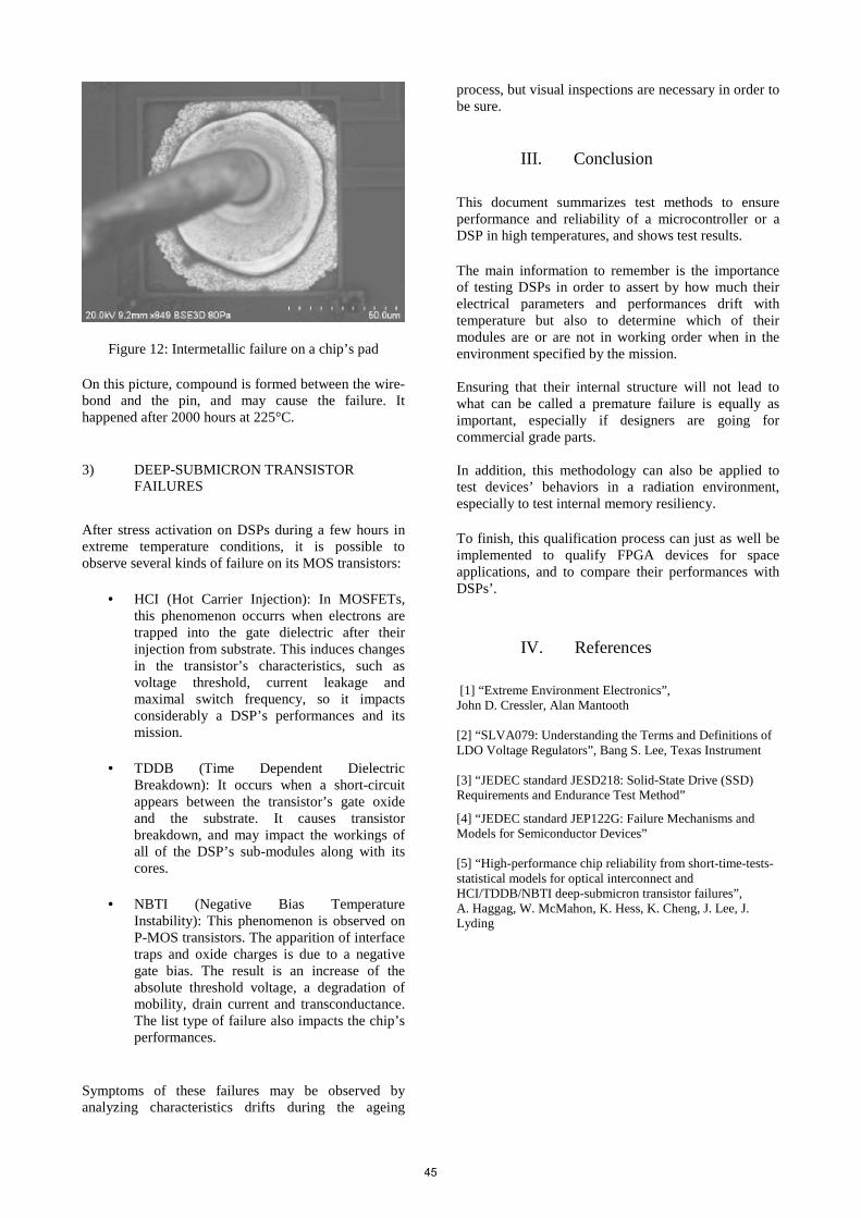
Figure 12: Intermetallic failure on a chip’s pad On this picture, compound is formed between the wire-bond and the pin, and may cause the failure. It happened after 2000 hours at 225°C.
3) DEEP-SUBMICRON TRANSISTOR FAILURES
After stress activation on DSPs during a few hours in extreme temperature conditions, it is possible to observe several kinds of failure on its MOS transistors:
• HCI (Hot Carrier Injection): In MOSFETs, this phenomenon occurrs when electrons are trapped into the gate dielectric after their injection from substrate. This induces changes in the transistor’s characteristics, such as voltage threshold, current leakage and maximal switch frequency, so it impacts considerably a DSP’s performances and its mission.
• TDDB (Time Dependent Dielectric Breakdown): It occurs when a short-circuit appears between the transistor’s gate oxide and the substrate. It causes transistor breakdown, and may impact the workings of all of the DSP’s sub-modules along with its cores.
• NBTI (Negative Bias Temperature
Instability): This phenomenon is observed on P-MOS transistors. The apparition of interface traps and oxide charges is due to a negative gate bias. The result is an increase of the absolute threshold voltage, a degradation of mobility, drain current and transconductance. The list type of failure also impacts the chip’s performances.
Symptoms of these failures may be observed by analyzing characteristics drifts during the ageing
process, but visual inspections are necessary in order to be sure.
III. Conclusion
This document summarizes test methods to ensure performance and reliability of a microcontroller or a DSP in high temperatures, and shows test results. The main information to remember is the importance of testing DSPs in order to assert by how much their electrical parameters and performances drift with temperature but also to determine which of their modules are or are not in working order when in the environment specified by the mission. Ensuring that their internal structure will not lead to what can be called a premature failure is equally as important, especially if designers are going for commercial grade parts. In addition, this methodology can also be applied to test devices’ behaviors in a radiation environment, especially to test internal memory resiliency. To finish, this qualification process can just as well be implemented to qualify FPGA devices for space applications, and to compare their performances with DSPs’.
IV. References
[1] “Extreme Environment Electronics”, John D. Cressler, Alan Mantooth [2] “SLVA079: Understanding the Terms and Definitions of LDO Voltage Regulators”, Bang S. Lee, Texas Instrument [3] “JEDEC standard JESD218: Solid-State Drive (SSD) Requirements and Endurance Test Method”
[4] “JEDEC standard JEP122G: Failure Mechanisms and Models for Semiconductor Devices” [5] “High-performance chip reliability from short-time-tests-statistical models for optical interconnect and HCI/TDDB/NBTI deep-submicron transistor failures”, A. Haggag, W. McMahon, K. Hess, K. Cheng, J. Lee, J. Lyding
45

Radiation Intelligent Memory Controller IP Core
P-X. Wanga , C. Selliera a 3D PLUS, 408 Rue Hélène Boucher, 78530 Buc, France
Abstract A radiation intelligent memory controller (RIMC) IP core
is proposed to work with a specific DDR2 SDRAM structure to reach a Radiation Hardened (RH) DDR2 SDRAM Solution. The IP core provides protection against Single Event Upset (SEU) and Single Event Functional Interruption (SEFI), combines the TID and SEL guarantee from the memory die to reach a hardened solution. This high performance RH DDR2 solution is suitable for all space applications such as commercial or scientific geo-stationary missions, earth observation, navigation, manned space vehicles and deep space scientific exploration.
I. INTRODUCTION DDR2 SDRAM is a very attractive technology for space
application thanks to its high density and high speed. However, o move it into space application, it is quite complicated to handle it because of the following reasons:
• Complex behaviour under radiation – No Rad Hard device available
• Volatile – Data loss risk if any functional issue • Difficult to handle Micro-BGA for Space
applications • Short life cycle – new device every 6 months That is the motivation to develop a RIMC IP core
provided a full protection against the DDR2 radiation soft effects such as SEFI and SEU. From user point of view, all radiation protections are transparent, and the RIMC provides a standard AMBA/DFI compatible interface to targeted most space FPGAs. Figure1 shows the solution’s architecture overview.
Figure 1: Overview
II. RIMC ARCHITECTURE The RIMC is defined by 2 interfaces (see Figure 2): • The user interface, AMBA compliant. This interface
contains at least one AHB bus, and may contain an
optional APB bus for user dynamic configuration. These busses are compatible to AMBA 2.0
• The DDR PHY interface, compliant to DFI 2.1 (depends on different FPGAs). This interface is used to send commands and data to the DDR components through the DDR PHY.
The RIMC controller can be configured by the core logic
using 2 different AMBA interfaces:
• Slave AHB interface with specific address mapping (1 area dedicated to DDR memory array and 1 area dedicated to internal registers)
• Slave APB interface dedicated to internal registers
Figure 2: RIMC Interface
The RIMC is highly configurable to be compatible with most of user designs:
• User data width (from x8 to x128) • Hamming or Reed-Solomon(RS) ECC selectable • Configurable up to 8 AHB slave interfaces • Configurable DDR2 ranks to increase memory
capacity • Clock & ODT setting compatible with 3D PLUS
modules • Capability to manage memory redundancy design The RIMC first version is to address FPGA development,
and it is fully commercial available.
46

III. PAGE NUMBERS MEMORY RADIATION ERRORS & IP CORE PROTECTIONS
The DRAM radiation errors can be simply classified as below in 2 categories: Hard Errors and Soft Errors. The Hard Errors create irreversible errors when the threshold or limit have been passed. 3D PLUS propose a radiation tolerant DDR2 memory die with the guarantee of TID>100Krad(Si) and SEL>60Mev.cm²/mg. This paper will not present detail results on TID & SEL guarantee of the memory die.
On the other hand, as semiconductor feature size scaling down, the soft errors (SEU and SEFI in case of DDR2) easily can be dominated events, especially SEFI, to DDR2 memories under radiation environment. However, each semiconductor, even each DDR2 Part Number from same semiconductor, will bring totally different SEU & SEFI results. To reach a real Rad-Hard DDR system, a well-evaluated specific DDR2 memory and its tailored controller, for example: identify memory different types of SEFI and select the correspondent mitigation strategies to guarantee no data loss, are mandatory.
A. IP Core SEU Mitigation The RIMC can be configured at different types of ECC
based on error rate tolerance, and here is an example of Reed-Solomon code as in figure 3 for 32b data and 50% overhead [RS(12;8), m=4, Global Bus = 48bits].
Figure 3: Example of data path with RS code, component Data Bus = 8 and DDR Data Bus = 32
As this RS ECC structure, The RIMC IP core(3D PLUS P/N: 3DIPMC700) can correct up to 8 bits error (row error) in one die per 48b, and 2 SEUs in the same address of different die per 48b. In case of scrubbing applied, the worst case (one particle create 2 upsets in 2 dice) in correctable error rate will be 3.8E-9 upset/day/module. Please note that 3DIPMC700 provides several different types of ECCs, and here is the error rate with Figure 3 data structure. The other ECCs (ex: Hamming) or other structures will bring other results.
B. IP Core SEFI Protection Single Event Functional Interruption (SEFI) - a condition
which causes a temporary non-functionality or interruption of normal operation induced by an energetic particle in the
affected device, are very critical to space design. Mentioned at the beginning of this chapter, as feature size scaling down, the modern DRAM components have lower SEFI threshold and bigger cross section, which makes the SEFI easily becoming the dominated event. Moreover, unlike the SEU correctable by ECC, SEFI can easily bring system interruption or data loss and damage the whole sub-systems.
Traditionally, SEFI mitigation is to power cycle or reset the component after SEFI happened, which means to restore or recover the component from a SEFI; However, power cycling will lead data loss, and in most case power lines are merged together, so not only the SEFI die data lost, but also all the dice managed by same power lines will have data loss.
To avoid all these negative impacts from SEFI, a patent-pending SEFI protect technique has been designed and embedded in RIMC IP Core to prevent SEFI to replace traditional “after SEFI happened and recover” strategy. This SEFI protection is transparent to user and integrated in the RIMC IP core. Verification test had been performed at Radiation Effects Facility, University of Jyväskylä, Finland (RADEF) to confirm the protection, here below is the result:
Table 1: 3D PLUS DDR2 Memory module SEFI results under RIMC Protection [1]
Ion LET [MeV/mg/
cm2]
Rang [micron
s]
Fluence [p/cm²]
Sample /Runs
SEFI
20Ne+6‡ 3.63 146 >1E6 1 No 40Ar+12‡ 10.2 118 >1E6 5 No 56Fe+15 18.5 97 >1E6 5 No 82Kr+22 32.2 94 >1E6 >10 No
131Xe+35 60.0 89 >1E6 6 No No SEFI observed till LET>60Mev-cm2/mg. As a general use purpose controller IP core, RIMC is
designed for any JEDEC standard DDR2 SDRAM. But please note that this patent-pending SEFI protection technique is not a universal solution, and only can be used to the die embedded in 3D PLUS DDR2 modules. On the other words, RIMC IP core can be used with any other DDR2 die, and the SEFI protection should be deactivated.
IV. CONCLUSION A RIMC IP core has been proposed to reach a radiation
hardened DDR2 solution. The solution includes the radiation tolerant DDR2 module with SEL immune and TID guarantee and RIMC IP core to specifically manage the SEU and SEFI of the DDR2 module to reach:
TID>100Krad(Si) SEL immune > 80Mev.cm2/mg SEU immune by design (3.8E-9 upset/day/module) SEFI immune by design (LET>60Mev-cm2/mg)
V. REFERENCES RADEF Cyclotron cocktail information: https://www.jyu.fi/ fysiikka/en/research/accelerator/radef/cocktail
47

DVB-S2 Software Defined Radio Modem
on the RC64 Manycore DSP
Peleg Aviely, Olga Radovsky and Ran Ginosar
Ramon Chips, Ltd., 5 HaCarmel Street, Yoqneam Illit 2069201, Israel
[peleg, olga, ran]@ramon-chips.com
Abstract
This paper describes high performance implementation of
DVB-S2 modem on the rad-hard manycore RC64 DSP.
Multi-level simulation and development methodologies are
described. Modem algorithms are specified, together with
implementation details. Efficient parallel processing is
enabled by the shared memory architecture, by PRAM-like
task oriented programming and by dynamic allocation of
tasks to cores. The modem achieves in excess of 2 Gbps
transmission and 1 Gbps reception.
I. INTRODUCTION
RC64 is designed as a high performance rad-hard manycore
DSP processor for space applications [1][8]. The architecture
is shown in Figure 1. 64 DSP cores (CEVA X1643) are
integrated together with hardware accelerators, a hardware
scheduler, multi-bank shared memory, a logarithmic network
on chip connecting the cores to the memories, and multiple
I/O interfaces.
RC64 is designed for space applications. Software Defined
Radio (SDR) and modems constitute very demanding
applications. This paper investigates the implementation of
DVB-S2/DVB-S2x modems on RC64. An LDPC hardware
accelerator is included in RC64 to support efficient modems,
and as a result RC64 achieves in excess of 2 Gbps transmit
rate and 1 Gbps receive rate. Earlier works in this area
include [6] and [7].
The RC64 DVB-S2 modem has been developed using a
multi-level methodology and simulators. The development of
a modem on a manycore processor combines communication
theory, parallel algorithm design, parallel programming and
profiling, and software engineering.
The paper presents the simulator, the modem algorithms,
implementation details, parallel programming of the model,
and performance evaluation.
Figure 1. RC64 Many-Core Architecture. 64 DSP cores,
modem accelerators and multiple DMA controllers of I/O
interfaces access the multibank shared memory through a
logarithmic network. The hardware scheduler dispatches fine
grain tasks to cores, accelerators and I/O.
II. RC64 DVB-S2 SIMULATOR
Figure 2 depicts the RC64 DVB-S2 simulator structure. The
data generator creates baseband frames. The transmitter
encodes and modulates the frames according to DVB-S2 and
DVB-S2X standards. The channel simulator adds noise and
impairments. The receiver demodulates and decodes the
signal, and the analyzer compares the sent and received
signals.
The simulator enables testing and performance optimization
regarding modem quality (bit error rate for a range of channel
impairments, signal to noise ratio and bandwidth), modem
48

bitrate (performance of RC64 executing the modem
application), bottleneck analysis (identify required
accelerator(s) for the modem) and hardware accelerators type
and capacity (validation before hardware integration).
RC64 TX simulator
Channel simulator
RC64 RX simulator
Data generatorand
Analyzer
Transmit data Receive data
Figure 2. RC64 DVB-S2 Simulator
Modem development is carried out through six levels of
refinement, as shown in Table 1. Algorithm development
starts by coding in Matlab a high level model of the modem,
and proceeds through stages until finally parallel C code is
employed to program the actual RC64. We start with an
unrestricted algorithm, implemented in Matlab (level 1). The
accelerators code is replaced by a Matlab executable (mex)
file generated from RTL descriptions of the accelerators.
Level 1 serves as golden model, to which subsequent level
models may be compared.
Level 2 takes into account architectural restrictions of RC64
such as limited memory and real-time constraints. For
instance, receiver input samples are processed in pre-defined
sample groups rather than in frame size sample groups. In the
third level, Matlab floating-point computations are replaced
by Matlab fixed point at a word precision of 16 bits,
compatible with high-speed arithmetic on the DSP cores of
RC64. Accelerator models are replaced by more precise ones
driven from RTL. Outputs are carefully compared with the
results of the floating-point models, to assure minimal signal
degradation.
At level 4, Matlab code is replaced by code in the C language,
compatible with the compiler for the DSP cores in RC64. The
Matlab simulator models of the transmitter and receiver are
replaced by models for the cycle accurate simulator of RC64,
executing the compiled C code. The output must be exactly
the same as produced in level 3. The accelerator code is a
function in C representing the hardware accelerator,
embedded in the cycle accurate simulator of RC64.
At level 5, the code is parallelized to execute on RC64 and
further optimizations are performed to take advantage of
specific hardware features of the DSP cores. The accelerators
function is executed as a separate task, in parallel with other
tasks. In level 6 the entire modem is executed on RC64
hardware
Table 1. Levels of Simulation and Modem Development
Level Level Name Language Precision Style Accelerators
1 High Level Modem Matlab Float Virtual unlimited architecture FloatC-to-mex
2 Matlab DSP Modem Matlab Float Restricted to real-time DSP of RC64
Restricted memory sizes
Translate input frames to samples on TX, input
sample stream to frames on RX.
FloatC-to-mex
3 Fixed Point Matlab
DSP Modem
Matlab Fixed 16 Rounding and saturated computation
Use CEVA lib functions
RTL-to-mex
4 C-Fixed Modem C Fixed 16 Bit-exact to Level 3 C function
5 C-Parallel Modem C Fixed 16 Compliant to Plural shared-memory programming
model [8]
C function as a
separate task
6 RC64 Modem C Fixed 16 Task on accelerator
hardware
III. RC64 DVB-S2 MODEM ALGORITHMS
In this section we describe the algorithms of the transmitter,
the communication channel, the receiver and the data
generator and analyzer.
A. Transmitter
The DVB-S2 and DVB-S2X transmitter includes the
following functional blocks to modulate input streams, as
specified and recommended in [2][3][4] (Figure 3): CRC-8
encoder, baseband (BB) header insertion and stream
adaptation, BB Scrambling, FEC encoding (comprising BCH
and LDPC encoders and bit interleaver), bit mapping into
constellations, physical layer framing (PL header insertion,
followed by pilot adding and scrambling) and BB shaping
(up-sampling and low-pass filtering). Output I/Q samples are
provided to two DACs, generating I and Q baseband signals.
This series of functional blocks can be clustered into Pre-
LDPC stage, the LDPC encoder, and Post-LDPC stage.
49

Figure 3. Functional block diagram of the DVB-S2 transmitter (following [3])
Figure 4. Channel simulation model
50

B. Communication Channel Simulation
Physical layer impairments in the communication channel
include those introduced by the channel, such as reflections
and interference, as well as those induced by various
components in the system, such as tuner I/Q imbalance and
amplifier non-linearity. These impairments degrade the
received SNR and may in some cases affect the convergence
behavior of various computation loops in the receiver.
In order to test the demodulator performance, different
realistic conditions that can affect the quality of received
signals are simulated. Physical layer impairments in DVB-S2
receivers are discussed in [4]. A simpler channel model is
implemented in Matlab (Figure 4 ). Every noise source is set
independently, allowing flexible channel simulation.
C. Receiver
The functional block diagram of DVB-S2 receiver according
to DVB-S2 guidelines [2] is depicted in Figure 6. The
Receiver application includes the following functional
blocks.
Signal Processing Chain
Adjacent Channel Filtering using BB FIR.
I/Q imbalance compensation, an iterative algorithm to
estimate I, Q and compensate for imbalance.
DC offset removal, using a simple IIR.
Frame Synchronization, using a 25 taps correlator and a
peak detector.
Symbol Timing Recovery, using a Farrow cubic
interpolator and a Gardner detector.
Decimator and Matched Filter.
Carrier Frequency Recovery (coarse and fine recovery)
based on a pilot. Coarse recovery employs a second order
feedback loop based on a delay-and-multiply frequency
error detector. Fine recovery employs a feed-forward (FF)
estimation algorithm, derived from the L&R (Luise and
Reggiannini) technique.
Phase Recovery (coarse and fine recovery), using FF ML
estimator.
Digital AGC, based on a pilot assisted vector tracker
mechanism.
LMS Equalizer, employing DFE with a small number of
taps.
Decoder Chain
Descrambler, identical to the TX scrambler
LLR calculation, finding the logarithm of the distance
between the soft symbol and the nearest hard symbol.
De-interleaver, identical to the TX interleaver.
LDPC Decoder, BCH Decoder, BB Descrambler and BB
Header CRC Decoder.
Similar to the transmitter, the receiver, too, may be clustered
into Pre-LDPC, LDPC and Post-LDPC stages. The RF Front
End, ADC and AGC blocks are not implemented in the
simulator. Figure 5 describes the state machine of the
receiver. Steady-state is entered when acquisition stages
complete successfully. The main computation during this
state consists of filtering, PHY descrambling, de-mapping
and de-interleaving. The FEC LDPC decoder is implemented
as a hardware accelerator. The rest of the computation
includes BCH decoding (in some cases), descrambling and
header decoding. In parallel, tracking is performed for the
next incoming frame, enabling fast reaction to channel
impairment changes, modulation changes and end-of-stream
detection.
Figure 5. Receiver state machine
The performance of the DVB-S2/DVB-S2X link (consisting
of transmitter, channel and receiver) is evaluated by the
signal analyzer (Figure 2). The signal analyzer compares
reconstructed bits with transmitted bits and calculates Frame
Error Rate (FER), Packet Error Rate (PER) and Bit Error Rate
(BER). In a communication chain without channel
impairments, the reconstructed data should be exactly the
same as transmitted. The DVB-S2 standard defines the
expected error performance for different modes. PER is the
ratio between the useful transport stream packets (188 bytes)
correctly received and affected by errors, after forward error
correction.
51

FEC Decoder
Signal Processing Chain
AFE Interface
I/QDown Sample
RF Front End
2XADCI
QIF
I
QDC Cancel
AGC
I/Q Imbalance
I
Q
Adjacent Channel Filtering
I
Q
Timing Recovery(Gardner)
Correlator + State
Machine
Coarse Freq.
CorrectionNCO dF
I/Q I/QXFine Freq. Correction
L&R
Coarse Phase
CorrectionI/Q DAGCI/Q
Fine Phase Correction
(PLL)I/Q
Equlaizer(DFE)
Slicer+LMS Loop
I/Q I/Q
PHYDescrambler
Soft Demapper
(Metric Calc)
De Interleaver
LDPC Decoder
BCH Decoder
BB DescramblerHeader
RecoveryI/Q
Soft Bits
I/Q
Frame sync
Figure 6. Functional block diagram of DVB-S2 Receiver
IV. MODEM IMPLEMENTATION
Details of modem implementation are described in this
section. We first discuss hardware accelerators, followed by
data streaming, scheduling and mitigation of overhead.
A. Accelerators
A major computation bottleneck was identified during
profiling of the fourth level of simulation (C-Fixed modem).
Forward error correction (LDPC encode/decode) was found
to limit the throughput of the modem when executed by the
cycle accurate simulator.
The bottleneck can be eliminated using hardware
acceleration, implemented either by a dedicated on-chip
accelerator or by an external accelerator (ASIC or FPGA).
RC64 was extended with on-chip LDPC encode/decode
hardware accelerator that is capable of 1 Gbps receive rate
and 2 Gbps transmit rate. A second accelerator was added for
turbo coding, required for DVB-RCS modem. Other types of
accelerators are supported by dedicated parallel interfaces to
external FPGA or ASIC.
B. Data Streaming
Early analysis of the shared memory capacity required for the
transmitter and receiver algorithms showed that special care
should be taken regarding buffers for intermediate data. The
transition between bit-stream representation and symbol and
sample representations of the data requires minimizing
buffering of symbol and sample representation of data frames
in favor of bit-stream representation when possible.
52

Shared Memory (4MByte)
Frames buffer queue
(Bit-stream)
Pre-LDPC compute
LDPC Encoder
Accelerator
Pre-LDPC frames buffer
queue(Bit-stream)
Post-LDPC frames buffer
queue(Bit-stream)
Post-LDPC compute
Output samples double buffer
(Sample-stream)
DMAOut
DMAIn
Shared Memory (4MByte)
Frames buffer queue
(Bit-stream)
Post-LDPC compute
LDPC Decoder
Accelerator
Post-LDPC frames buffer
queue(Bit-stream)
Pre-LDPC double buffer(LLR stream)
Pre-LDPC compute
Input samples double buffer
(Sample-stream)
DMAIn
DMAOut
Transmit data flow
Receive data flow
Figure 7. Modem data flow
Buffering structure, modeled within the fourth level of
simulation (Table 1), define the partitioning of parallel
activity of the transmit and receive applications as described
in Figure 7, indicating buffering in shared memory. Bit-
stream representation of the data enables the most efficient
storage in shared memory, accessed as byte stream by the
DMA and DSP cores. A normal size frame is about 8 Kbyte
long. LLR-stream employs 16 bits to represent each data bit,
accessed as word stream by the DMA and the DSP cores.
Thus, a normal size frame occupies 128 Kbyte. Sample-
stream representation requires 16 bits per sample. Sample
representation depends on symbol count (due to different
possible constellations) and interpolation factor. A normal
size frame, in sample representation, occupies between 128
Kbyte (QPSK) and 32 Kbyte (256APSK). Memory allocation
is optimized by minimizing the buffer size for the sample-
stream.
C. Scheduling
The compute sequence for both transmitter and receiver is
driven by the transmit/receive sample rate. A continuous
sample stream must be transmitted to the DAC or received
from the ADC using DMA. Figure 8 presents the iterative
task graph used for scheduling the tasks (initial and final parts
are eliminated for clarity). When fully utilized, the modem
iteratively performs the following steps.
Get-data through input interface (ADC for receive, digital
interface for transmit).
Pre-LDPC compute stage, processing multiple frames
each iteration. The number of frames is limited by frame
size, data rate, available storage and available incoming
data.
LDPC stage that encodes or decodes data from the Pre-
LDPC stage.
53

Post-LDPC compute stage processing multiple frames
each iteration.
Put-data through output interface (DAC for transmit,
digital interface for receive).
Figure 9 presents the double buffer queues used for
supporting parallel operation during each iteration of the
transmitter. The input stream DMA stores data into one of the
two queues dedicated for input frames. The Pre-LDPC tasks
process concurrently the queue of input frames from the
previous iteration and store the results into one of the two Pre-
LDPC queues. The LDPC encoder accelerator processes the
data in its input queue and stores the result in one of its output
queues. The Post-LDPC tasks process concurrently the post-
LDPC queue of the previous iteration and store the results
into one of the two output sample queues. Finally, the output
stream DMA reads samples data and outputs the samples. By
the end of each iteration, input queues becomes output queues
(double buffers are switched), and the next iteration may start
Get DataPre-LDPC
LDPCPost-LDPC
Put Data
Iterationcontrol
Figure 8. Task map for transmit/receive application
54

Input framesdouble-buffer
queue
Pre-LDPCdouble-buffer
queue
Input frames
LDPC Encode
Accelerator
Input stream DMA
Output stream DMA
Start of iteration kPost-LDPC
double-buffer queue
Output samples
double-buffer queue
Frames of iteration k
Frames of iteration k-1
Frames of iteration k-2
Frames of iteration k-3
Samples of iteration k-4
Input framesdouble-buffer
queue
Pre-LDPCdouble-buffer
queue
LDPCEncode
Accelerator
Input stream DMA
Output stream DMA
End of iteration kPost-LDPC
double-buffer queue
Output samples
double-buffer queue
Frames of iteration k
Frames of iteration k-1
Frames of iteration k-2
Frames of iteration k-3
Samples of iteration k-4
Output Samples
DMA
Pre-LDPC task in cores
LDPC Accelerator
Post-LDPC task in cores
Figure 9. Iterative computation during transmit
Core #0
Core #3Core #4
Core #7LDPC Encoder
(a) Unbalanced load on 8 cores
Core #0
Core #3Core #4
Core #7
(b) Fine grain and work distributionhelp to balance
the load on 8 cores
LDPC Encoder
Core #0
Core #3Core #4
Core #35
(c) Shorter iteration time on 36 cores
LDPC Encoder
Core #0
Core #7Core #8
Core #50
(d) Even shorter execution time
on 51 cores; higher parallelism
of both tasks
LDPC Encoder
Pre-LDPC task in cores
LDPC Accelerator
Post-LDPC task in cores
iteration time iteration time iteration time iteration time
Figure 10. Alternative schedules for load balancing
55

Figure 10 presents load balance scheduling alternatives for
the three types of tasks using available processing resources
(LDPC accelerator and DSP cores). In (a), four cores execute
Pre-LDPC tasks and four other cores execute Post-LDPC
tasks, in parallel with the LDPC encoder. The Post-LDPC
tasks constitute a bottleneck. In (b), the Post-LDPC tasks are
broken up into 32 instances of fine grain tasks. Once Pre-
LDPC jobs are completed, Post-LDPC instances are allocated
to all eight cores and computation is accelerated. In (c), 36
cores are made available, all instances are allocated at the
same time, and Pre-LDPC becomes the bottleneck. Last, in
(d), the Pre-LDPC tasks are split into eight smaller tasks and
additional cores are made available. Consequently,
computation time is shortened.
D. Overhead mitigation
Ideal modem implementation, when execution is most
efficient and iteration time is minimized, depends on the
following architectural aspects.
Scheduling overhead minimized—When a many-core
solution is required to perform fine grain tasks to accelerate
computation such as in Figure 10 (d), the time between task
executions on cores must be negligible compared to tasks
duration. RC64 scheduler offloads this activity from run-time
software, and provides minimal overhead for task switching
time. The overhead relates to both allocating multiple
available tasks to many cores, as well as to recognition of task
terminations. Task terminations enable new task allocations,
which happens every iteration in such iterative task graphs.
Shared memory access efficiency—Dynamic scheduling of
tasks to cores, requiring cores to perform different code with
different data along each iteration, makes shared memory
access latency and throughput critical. Shared memory
phenomena such as data read hot-spots call for special care,
to prevent serialization in memory access. In some cases,
when data handling is interface dependent, queue
management requires critical section handling for inter-core
synchronization. The RC64 multi-bank and network on chip
optimize memory access by cores. The memory appears as a
flat address space, flexible for any type of data-set allocation
very similar to the PRAM model, significantly simplifying
the programming model.
Shared memory coherency—The programming model and
non-preemptive run-to-completion tasks enable keeping
shared memory with coherent data available for next task
allocation. Each core is responsible for storing all its
computational results into shared memory (using write-
through cache) before the task terminates. It then invalidates
its data caches automatically before starting a new task that
may accidently use the wrong data content in its cache. This
storing activity is supported in RC64 by its write-through
cache configuration of the DSP cores, together with the
minimal invalidation overhead at task terminations.
Local core computing efficiency—Processing cores
computing efficiency may suffer due to low compute-to-data
ratio or due to inefficient cache behavior. A major efficiency
factor is using the VLIW and SIMD capability to achieve
peak performance. RC64 cores are optimized for DSP
computations, having four multiply-accumulate functional
units along with two load/store units and two additional
general purpose instruction units. A main compute-intensive
part of the modem is the filters. Each DSP can perform a
complex multiplication every cycle continuously, as long as
the memory system can deliver the data. The local data
memory (cache and scratchpad) supports 16Kbyte data and
8Kbyte program memory, sufficient for many algorithms.
Data streaming efficiency—Data in shared memory should
be available for parallel memory read access to any of the
cores during each iteration. Output data queues in shared
memory should be accessible efficiently and concurrently by
any of the cores for writing during each iteration. Streaming
data to and from shared memory queues must not degrade the
computing throughput. RC64 DMA controllers are optimized
for this purpose, both for memory buffer management in
shared memory and for very high throughput to and from
shared memory, without degrading memory access rate by
the cores. Many DMA controllers can operate concurrently
to serve many different I/O activities.
Programming model simplicity—Programming a many-core
processor can become a very complex undertaking, requiring
deep knowledge of the micro-architecture and the special
mechanisms for solving the above challenges. RC64 task
oriented programming model emphasize parallel code
decomposition for application acceleration, in accordance
with algorithm and memory capacity requirements. Other
issues, such as shared memory access efficiency, coherency
and streaming may incur only minor effect on performance,
while the application developer enjoys a PRAM-like
abstraction, similar to a single core program design.
V. PERFORMANCE
This section reports performance results as computed with
the RC64 DVB-S2 simulator and cycle-accurate simulations
of RC64 [8].
A. Transmitter Performance
When simulating transmission of short frames using 32APSK
modulation and LDPC code of 8/9, the Pre-LDPC stage
requires 16,000 cycles, LDPC encoding takes 560 cycles, and
Post-LDPC is 100,000 cycles. Since there are 3402 32APSK
symbols in a short frame, Post-LDPC can be considered as
incurring 30 cycles per symbol. As shown in Figure 11, a
useful balance between pre-LDPC and post-LDPC can be
achieved with nine frames per iteration for pre-LDPC,
generating a total of 3402×9=30,618 symbols. Parallel
processing of these symbols in Post-LDPC tasks is achieved
by the remaining 55 cores. Each Post-LDPC task processes
30,618/55=557 symbols, taking 557×30=16,710 cycles. This
schedule translates to a data rate of
14232 [𝑏𝑖𝑡]∙9 [𝑓𝑟𝑎𝑚𝑒𝑠]∙300 [𝑀𝐻𝑧]
16710 [𝑐𝑦𝑐𝑙𝑒𝑠]= 2.3 𝐺𝑏𝑝𝑠 .
56

Each symbol contains two samples, and there are 6,804
samples per frame. The sample output rate is
6804 [𝑠𝑎𝑚𝑝𝑙𝑒𝑠]∙9 [𝑓𝑟𝑎𝑚𝑒𝑠]∙300 [𝑀𝐻𝑧]
16710 [𝑐𝑦𝑐𝑙𝑒𝑠]= 1.1 𝐺𝑠𝑎𝑚𝑝𝑙𝑒𝑠/𝑠 .
Another way of estimating performance is based on
considering that 116,000 cycles are required to process
14,232 data bits at 300M cycles/sec, and 64 cores are
available, or:
64 ×14,232 [𝑏𝑖𝑡]
116,000 [𝑐𝑦𝑐𝑙𝑒]×
300𝑀 [𝑐𝑦𝑐𝑙𝑒]
[𝑠𝑒𝑐]= 2.3 𝐺𝑏𝑝𝑠
The accuracy of these performance estimates is expected to
be within 30% of actual performance, based on simulator
accuracy and code optimization.
B. Receiver Performance
When receiving short frames in a steady state, the receiver
spends 220,000 cycles in the Pre-LDPC stage, 4,000 cycles
on average in the LDPC decoder, and 32,000 cycles in Post-
LDPC. The schedule of Figure 12 shows 8,000 cycles per
iteration, receiving two frames per iteration, using 54 DSP
cores to perform Pre-LDPC, eight DSP cores to perform Post-
LDPC. The resulting bitrate is
14,232 [𝑏𝑖𝑡] ∙ 2 [𝑓𝑟𝑎𝑚𝑒𝑠] ∙ 300 [𝑀𝐻𝑧]
8,000 [𝑐𝑦𝑐𝑙𝑒𝑠]= 1 𝐺𝑏𝑝𝑠.
16K cycCore #0Time
Core #8Core #9
Core #63
Iteration time=16.7K cyc
16K cyc
LDPC Encoder16.7K cyc
6K cyc
16.7K cyc
16.7K cyc
16K cyc
Figure 11. Transmit performance (32APSK, LDPC 8/9)
8K cycCore #0Time
Core #7Core #8
Core #63
Iteration time=8K cyc
8K cyc
LDPC Decoder8K cyc
8K cyc
8K cyc
8K cyc
8K cyc
Figure 12. Receive performance (32APSK, LDPC 8/9)
VI. CONCLUSIONS
We have described a high-performance implementation of
DVB-S2 transmitter and receiver on RC64, predicted to
exceed 2Gbps transmission and 1Gbps reception. A six-
levels development and simulation process has been
described. Dynamic scheduling of tasks to cores, using the
hardware scheduler and based on task oriented programming,
resulted in a flexible solution that can easily be adapted to
other modem parameters and other standards.
ACKNOWLEDGEMENT
Funding has been provided in part by Israel Space Agency
and by the European Union's Seventh Framework Program
for research and demonstration under grant agreement no.
607212 (MacSpace)
REFERENCES
[1] Ran Ginosar and Peleg Aviely, RC64 – Many-Core
Communication Processor for Space IP Router. In Proceedings
of International Astronautical Conference, pp. IAC-15-B2.6.1.
Jerusalem, Israel, Oct. 2015.
[2] DVB (2005). User guidelines for the second generation system
for Broadcasting, Interactive Services, News Gathering and
other broadband satellite applications (DVB-S2). User
guidelines ETSI TR 102 376 V1.1.1 (http://www.etsi.org).
[3] Morello, Alberto, and Vittoria Mignone. "DVB-S2: The second
generation standard for satellite broad-band services."
Proceedings of the IEEE, vol. 94, no. 1, pp. 210-227. IEEE,
2006.
[4] Nemer, Elias. "Physical layer impairments in DVB-S2
receivers." In Second IEEE Consumer Communications and
Networking Conference, CCNC, pp. 487-492. IEEE, 2005.
[5] Savvopoulos, Panayiotis, Nikolaos Papandreou, and Th
Antonakopoulos. "Architecture and DSP Implementation of a
DVB-S2 Baseband Demodulator." In Digital System Design,
57

Architectures, Methods and Tools, 2009. DSD'09. 12th
Euromicro Conference on, pp. 441-448. IEEE, 2009
[6] Beadle, Edward R., and Tim Dyson. "Software-Based
Reconfigurable Computing Platform (AppSTAR TM) for
Multi-Mission Payloads in Spaceborne and Near-Space
Vehicles." In International Conference on Reconfigurable
Systems and Algorithms. ERSA 2012.
[7] Dalio, B. A., and K. A. Shelby. "The implementation of OFDM
waveforms on an SDR development platform supporting a
massively parallel processor." In SDR'09: Proceedings of the
Software Defined Radio Technical and Product Exposition.
2009.
[8] Ginosar, Ran, Peleg Aviely, Tsvika Israeli and Henri Meirov.
“RC64: High Performance Rad-Hard Manycore.” DSP Day,
2016.
58
Session 5:
DSP Software and Applications
59

DSP Benchmark Results of the GR740 Rad-Hard Quad-Core LEON4FT
Topics: Status and results of DSP related ESA contracts, Space qualified DSP components
Javier Jalle, Magnus Hjorth, Jan AnderssonCobham Gaisler, Kungsgatan 12, SE-411 91, Göteborg, Sweden
Tel: +46 31 775 86 50{javier.jalle,magnus.hjorth,jan.andersson}@gaisler.com
Roland Weigand, Luca FossatiEuropean Space Agency, Keplerlaan 1 – PO Box 299, 2220AG Noordwjik ZH,
The Netherlands, Tel: +31 71 565 65 65{roland.weigand,luca.fossati}@esa.int
ABSTRACT
The GR740 microprocessor device is a SPARC V8(E)based multi-core architecture that provides a significantperformance increase compared to earlier generations ofEuropean space processors. The device is the result theEuropean Space Agency's initiative to develop aEuropean Next Generation Microprocessor (NGMP).
Engineering models have been manufactured in 2015and tested during the first quarter of 2016. Spacequalification of flight models is planned to start in thesecond half of 2016. GR740 is the highest performingEuropean space-grade general purpose microprocessorand, due to the presence of four powerful floating-pointunits, it is suitable for executing DSP applications. Thisabstract provides an overview of the GR740 and asubset of the benchmarks used within the ESA activity'sfunctional validation effort.
BACKGROUND
The LEON project was started by the European SpaceAgency in late 1997 to study and develop a high-perfor-mance processor to be used in European space projects.Following the development of the TSC695 (ERC32) andAT697 processor components in 0.5 and 0.18 μm tech-nology respectively, ESA initiated the Next GenerationMicroprocessor (NGMP) activity targeting a EuropeanDeep Sub-Micron (DSM) technology in order to meetincreasing requirements on performance and to ensurethe supply of European space processors. CobhamGaisler was selected to develop the NGMP system thatis centred around the new LEON4FT processor.
Throughout 2014 and 2015, the architecture was de-signed and manufactured in the C65SPACE platformfrom STMicroelectronics [4]. This chip, now calledGR740, constitutes the NGMP Engineering Model. Be-sides the chip development, the existing SPARC soft-ware development environment has been extended withsupport for the GR740.
Figure 1: GR740 Block diagram
60

ARCHITECTURAL OVERVIEW
Figure 1 shows an overview of the GR740 architecture.The four LEON4FT processors are connected to ashared bus which connects to a 2 MiB EDAC protectedLevel-2 cache before reaching external EDAC protectedSDRAM. Each LEON4FT processor has a dedicatedpipelined IEEE-754 floating-point unit. While theGR740 implementation of LEON4FT lacks support fordedicated multiply-and-accumulate instructions this ismitigated by the presence of the large number ofprocessor registers, L1 cache memory and highoperating frequency.
The main communication interfaces of the deviceinclude eight external SpaceWire ports connected to anon-chip SpaceWire router, two 10/100/1000 MbitEthernet ports, MIL-STD-1553B and 32-bit PCI.
The design makes use of extensive clock gating for thecommunication interfaces and the processors, that canbe put in a power-down mode to conserve power whensome or all cores are unused.
The four parallel CPU / FPU cores, each running ondedicated separate instruction and data L1 caches(Harvard architecture), at 250 MHz clock frequency, cantheoretically provide up to 1 Gflop/s in single or doubleprecision. Together with the multiple Spacewire andEthernet interfaces, this makes the GR740 suitable forDSP applications, provided that the applicationimplementation succeeds in making an efficientparallelisation and streaming of data across the sharedon-chip buses. This can be demonstrated with theimplementation of dedicated DSP benchmarks, as forexample those suggested in [1].
The NGMP architecture has already been evaluated inan effort where the GAIA VPU application was adaptedto take advantage of a multi-core system. Theconclusion from this effort was that the GR740 is fastenough to run the GAIA VPU application [2].
FUNCTIONAL VALIDATION AND DSPBENCHMARKS
The functional validation of the GR740 device builds onexisting tests used in the frame of the NGMP activities.The tests include both functional and performancebenchmarks.
PARSEC 2.1 benchmarks: PARSEC are a set of multithreaded shared-memory benchmarks. We run them with different number of cores. To show the benefit of multiple cores, we calculate the speedup as:
where T1 is the execution time with one core and
T2 the execution time with different number of cores.
In an ideal parallel application with no overheads, the speedup obtained with 4 cores would be 4x. Figure 2 shows the speedup of a set of the PARSEC 2.1 small workloads under Linux. We observe an speedup up to almost 3.5x on the swaptions benchmark and 1.83x on average for the 4 cores.
Barcelona Supercomputing Center Multicore OS benchmarks: These benchmarks were designed to evaluate the multicore interference for different OS [5]. We use a subset of the benchmarks that continuously access the L2 cache with different patterns: L2-128K and L2-256K use 128K and 256K of L2 space, L2-miss is designed to miss on the L2 cache and ST performs store operations that hit on the L2 cache. These four benchmarks are highly sensitive to interference when running in multicore. We execute these benchmarks in single core without interference and with all other cpus running L2-miss to generate an extreme interference scenario. We calculate the slowdown (as the inverse of the speedup) which effectively measures the impact of the interference that the cores are generating. Figure 3 shows the slowdown for the above mentioned benchmarks. We observe that the slowdown reaches up to almost 3.1x for the ST benchmark, which is the most sensitive since in the absence of interference, store operations are very efficient due to the write-buffers.
Sup=T 1
T 2Figure 3: BSC Multicore OS benchmarks slowdown
Figure 2: PARSEC benchmarks speedup
61

EEMBC benchmarks: We have successfully compiledand run EEMBC CoreMark, Autobench, FPMark andMultibench benchmark suites. In this paper, we presentthe results of the Coremark and Autobench suites whichmight be interesting for a DSP audience. In order to compare the GR740 with previous LEONprocessors, we run the Coremark in a single core on theUT699, GR712 and GR740. Figure 4 shows theCoreMarks [3] when running in a single core. We cansee a significant increment on the GR740 with respect tothe previous processors, mainly due to the frequencyincrement (250 MHz vs 50 MHz). This increment wouldbecome even bigger if we consider the four cores incomparison with the 2 core GR712RC or the singlecoreUT699.
Figure 5 shows the iterations/sec of the EEMBCAutobench suite under singlecore Linux OS, whichallows to compute an AutoMark score of 111.97,comparable with the scores shown in [3].
CCSDS 123 Image Compression: This softwareimplements the lossless multispectral & hyperspectralcompression according to the draft standard CCSDS123.0-R-1. We have run 4 compressions under Linuxusing one and four cpus, showing an speedup factor of3.43x.
CONCLUSION
The GR740 is a SPARC V8(E) based multi-corearchitecture that provides a significant performanceincrease compared to earlier generations of Europeanspace processors, with high-speed interfaces such asSpaceWire and Gigabit Ethernet on-chip. The platformhas improved support for profiling and debugging, andsoftware tools have been upgraded to this newarchitecture. Moreover, a rich set of software isimmediately available due to backward compatibilitywith existing SPARC V8 software and LEON3 boardsupport packages.
The GR740 constitutes the engineering model of theESA NGMP, which is part of the ESA roadmap forstandard microprocessor components. It is developedunder ESA contract, and it will be commercialised underfair and equal conditions to all users in the ESA memberstates. The GR740 is also fully developed withmanpower located in Europe, and it only relies onEuropean IP sources. It will therefore not be affected byUS export regulations.
The functional validation effort aims to validatefunctionality of the device and of the developmentboard that will be made available to the space industry.
The GR740 is the highest performing Europeanspace-grade processor to date and results of DSP
benchmarks will be presented to allow industry to assessthe GR740's suitability for DSP applications.
News about the GR740 device can be found at thefollowing link:
http://www.gaisler.com/gr7 40
REFERENCES
[1] Next Generation Space Digital Signal ProcessorSoftware Benchmark , Issue 1.0,TEC-EDP/2008.18/RT, 01 December, 2008
[2] RTEMS SMP Executive Summary, Issue 1, Revision 2, RTEMSSMP-ES-001, March 2015, http://microelectronics.esa.int/ngmp/RTEMS-SMP-ExecSummary-CGAislerASD-OAR.pdf
[3] EEMBC – The Embedded Microprocessor Benchmark Consortium http://www.eembc.org/
[4] P. Roche, G. Gasiot, S. Uznanski, J-M. Daveau, J. Torras-Flaquer, S. Clerc, and R. Harboe-Sørensen, “A Commercial 65 nm CMOS Technology for Space Applications: Heavy Ion, Proton and Gamma Test Results and Modeling”, IEEE TRANSACTIONS ON NUCLEAR SCIENCE, VOL. 57, NO. 4, AUGUST 2010
[5] Francisco J. Cazorla et. al. Multicore OS benchmarks. Technical Report Contract 4000102623, European Space Agency, 2012.
Figure 5: EEMBC automotive benchmarks
Figure 4: Coremarks per core for different LEON processors
62
A Lightweight Operating System for the SSDP
A. Luntzera
, F. Kerschbauma
, R. Ottensamera
, C. Reimersa
aDepartment of Astrophysics, University of Vienna, 1010 Vienna, Austria
Abstract
The Department of Astrophysics at the University of Vienna is
a provider of payload instrument flight software. Among the
projects under development is a custom, lightweight operating
system for the upcoming Scalable Sensor Data Processor
(SSDP) based on prior experience with its predecessor, the
Massively Parallel Processor Breadboard (MPPB). The
objective of this project is to create easy to use software that
is capable of efficiently driving the SSDP’s Xentium DSP
cores. Through its unique concept of driving the DSPs, it
allows the user to make full use of the resources of this
specific platform.
I. INTRODUCTION
A common problem of space missions is the limited
processing power of available space-qualified hardware, as
Payload data processors of on-board spacecraft and satellites
are subject to high levels of radiation. While there is the
LEON to fill the role of a general purpose processor (GPP),
the only radiation hardened digital signal processor (DSP)
available in Europe is the already dated ADSP-21020, if
ITAR/EAR regulations are taken into account.
The need for a new processor or System-on-Chip (SoC)
computer design for on-board payload data processing is high.
This is mainly due to the ever increasing quantity of sensor
data, as modern instruments produce ever larger volumes of
measurements. Available down-link bandwidth however, is
limited by available power, antenna sizes and in the end,
physics.
In recent years, ESA has been pursuing the development
of a next generation payload processor. One of the outputs of
this effort is a prototype SoC called the MPPB (Massively
Parallel Processor Breadboard) developed by Recore Systems
under ESA contract 21986 [1]. The MPPB is built around a
Very Long Instruction Word DSP architecture named Xentium.
In this platform, a LEON processor is acting as a supervisor,
controlling a Network-on-Chip (NoC) with multiple DSPs,
memory and I/O devices attached to it.
II. MOTIVATION
In the course of the NGAPP (Next Generation Astronomy
Processing Platform) activities, an evaluation of the MPPB
was performed in a joint effort of RUAG Space Austria
(RSA) and the Department of Astrophysics at the University
of Vienna (UVIE). While the original intent of the work of
UVIE was to quantify the performance of the Xentium DSPs
and the MPPB as a whole with regard to on-board data
treatment and reduction in an astronomical mission setting, it
was found that, given the highly innovative nature of this new
processing platform, a novel approach was needed concerning
the management of system resources, DMA mechanics and
DSP program design for best efficiency and turnover rates.
Consequently, the University of Vienna developed an
experimental operating system to stably drive the DSP cores
and the MPPB close to its performance limit. This was
achieved by splitting processing tasks into a pipeline of small
units (kernels) that are dynamically scheduled to run on the
Xentium DSPs, as required by the amount of data in the
pipeline stages, thereby overcoming bottlenecks resulting
from memory transfer overheads and cache sizes that would
inevitably emerge when using large, monolithic programs
with the particular characteristics of the MPPB.
At present, activities are carried out by Thales Alenia
Space España and Recore Systems in an effort to create the
Scalable Sensor Data Processor (SSDP) hardware, where an
ASIC is being developed based on the MPPB 2.0, which is an
update of the original MPPB with adapted specification [2].
This new implementation was made available to UVIE in Q1
2016 as a firmware update to the existing MPPB hardware
box.
In order to support this new hardware, a more refined
version of the experimental operating system is under
development at the University of Vienna under a nationally
funded ASAP 11 project, which also aims to become space-
qualifiable, supporting applicable documentation and S/W
standards.
The software is tailored to the NoC concept present in the
SSDP and is optimised for best performance in key areas of
system and resource management. These include fast and
efficient interrupt handling to ensure low response times and
high memory throughput for DMA transfers that service the
Xentium data caches and fast I/O interfaces like SpaceWire or
ADC/DAC.
Supporting functionality, for example device drivers,
threads and schedulers, timing and a system
configuration/information interface will be provided. Great
effort is made to keep CPU and memory footprints at a
minimum, so the LEON processor is available for duties other
than DSP and data processing control, such as handling of
tele-commands or instrument-related control tasks.
63

A major aim is to make the operating system as easy to use
as possible, by providing appropriate, well designed interfaces
in order to keep the need for configuration and extra
programming effort at a minimum.
To encourage use, modification and redistribution of the
operating system, it will be made available under an open-
source license, including all drivers, modules and example
DSP program kernels, as well as the documentation.
III. SSDP/MPPB 2.0 HARDWARE OVERVIEW
The MPPB 2.0 (hereafter referred to as just MPPB)
platform is a representative "preview" of the future SSDP
hardware. It consists of two VLIW DSPs, called Xentiums,
which are connected to a high-speed Network-on-Chip (NoC)
along with distributed SDRAM memories and external high-
speed interfaces, such as SpaceWire, to satisfy requirements
for space-based platforms. Attached to the NoC is a
conventional AMBA bus, which serves as an inter-connect for
a LEON GPP. The LEON is intended to control, manage and
serve the nodes of the NoC and other payload oriented
interfaces (e.g. the real time clock). It can also be used to run
legacy software for satellite control operations beside its NoC
servicing tasks. The system is clocked at 50 MHz.
A. Network-on-Chip
In high-performance multi-core computing, input/output
bandwidth and data transport capability are most critical
issues. In the MPPB, this is addressed by a Network-on-Chip
(NoC), which is a packet-switched network based on an XY
routing scheme. XY routing is a simple method of routing
packets through a network, where first the horizontal (X)
direction is taken, followed by a turn to the vertical (Y) path
at the targets X location. For this reason, the forward and
return paths are different most of the time and are guaranteed
to be safe from deadlocking.
The 3x3 NoC mesh connects the following devices:
2 Xentiums,
a bridge to the ADC/DAC
an 8-channel DMA controller
2 SpaceWire connections
DDR (SDRAM) controller
SRAM memory tile
AMBA Subsystem
Every mesh routing node has 5 ports and serves 4 channels
per port, each of them with different priorities. A channel
offers a bandwidth of 1.6 Gbit/s at a system clock of 50 MHz.
Two high-priority channels are dedicated to DMA transfers,
while the low-priority channels serve single read/write
operations and interrupts. The high-bandwidth design is
important to the NoC concept, which intends to contain all
high-volume data flows to the network, never crossing the
slow AMBA bridge.
B. Xentium DSP
The Xentium is a little-endian Very Long Instruction Word
(VLIW) type digital signal processor IP core developed by
Recore Systems, The Netherlands.
A Xentium DSP consists of three main parts: the Xentium
local bus, the data path (processing core) and a tightly-
coupled memory (TCM) bank composed of 4 sub-banks of
8 kiB each. The Xentium local bus is an AHB-like bus that
allows the attachment to already existing compatible hardware
if needed.
Most instructions work on 32 bit or pairs of 16 bit
complements of data-words. The different units offer different
functionality:
A0, A1 32 bit and 2x16 bit arithmetic with 40 bit wide add
registers
S0, S1 32 bit and 2x16 bit arithmetic with 40 bit wide add
registers, shift operations
M0, M1 multipliers for 32-bit operands or 2x16-bit operands
E0, E1 load/store functionality
C0 32 bit and 2x16 bit arithmetic, loop and branch control
instructions
P0 32 bit and 2x16 bit arithmetic, compare and packing
instructions
The TCM provides access to 4 different memory banks at
the same time. As the data path can load and/or store 4x32 bit
values simultaneously using these banks, enough bandwidth is
available to all different parallel execution units in the
Xentium.
IV. FUNDAMENTAL REQUIREMENTS OF THE OS
A set of core prerequisites that are crucial to the usability
of an operating system has been identified and are described
in short below. These are not unusual for an operating system
of this category, the features that are particular or less
common are presented in more detail in the next sections.
A. Interrupts and Traps
CPU traps are a central element in the run-time
environment of the SPARC architecture, they provide means
to treat hardware exceptions and interrupt requests. Interfaces
to manage and install higher level trap handlers are available
and default handlers for different traps typed are provided.
Effort is made to reduce interrupt entry and exit times as
much as possible, as the SSDP tends to have higher rates than
comparable systems under load. This is a consequence of
necessary signalling with the Xentium DSPs and other
platform-specific devices, so reducing even small amounts of
systematic overhead can have great effects in the long run.
64

Interrupt call-back support for both hardware and software
interrupts are provided. These will not only allow fast and
easy (de-)registration of an arbitrary number of call-backs per
interrupt with associated user-data, but also deferred low-
priority interrupt handling in a dedicated thread or OS idle
loop.
B. Multi-Core Support
In order to make it future-proof and interesting for use
with other LEON-based platforms, the OS is written with
multi-core support in mind, including dedicated per-CPU
interrupt stacks, cross-CPU synchronisation and locking, as
well as task migration with according support in the threading
library.
C. Timers
In addition to the usual facilities, emphasis is put on tick-
less (i.e. non-periodic) timing functionality, so unnecessary
wake-ups of the GPP and inherent waste of CPU cycles can
be avoided.
D. Threads and Schedulers
Along fixed priority based scheduling, a modified earliest
deadline first scheduler with priority execution in overload
conditions is implemented. This, along with dynamic ticking,
gives an option to optimise thread CPU utilisation with the
added benefit of predictable execution for certain high-
priority threads in conditions, where the total load
unexpectedly exceeds 100%.
E. DMA Driver
The 8 channels of the DMA 2D-transfer feature in the
MPPB/SSDP are essential to its computational performance.
Low overhead and ease of use are desirable for this driver.
Special care must be taken to avoid access conflicts to
channels since the Xentiums have gained the faculties to
receive transfer-completion signalling with version 2 of the
MPPB and can now be used to initiate transfers themselves,
thereby reducing the interrupt load of the GPP significantly.
As there are (by the nature of the NoC) no atomic loads/stores
possible, the usage state of a DMA channel might change
unexpectedly during programming, if channels are
dynamically used, rather than being statically assigned to
either a DSP or the GPP. The former is clearly more desirable,
as there is less downtime when more transfers need to be
started than channels are assigned to a node.
F. I/O Interface Drivers
The major I/O devices, i.e. ADC/DAC and SpaceWire that
are common to both the MPPB and the SSDP are supported,
others (FLASH, GPIO, LEDs, LCD, ...) as they are present or
needed for OS operations or development support.
G. FDIR and Error Reporting
Fault detection and recovery with regard to hardware
devices is part of the drivers themselves. EDAC handling and
memory scrubbing is present as part of the OS. A central error
reporting facility is in place that is being used by drivers or
other software components.
H. Miscellaneous
Additional functionality to support application software
development is available. This includes an interface to the
debug support unit (DSU) of the LEON, generation of stack
traces and register dumps on hardware traps, along with any
NoC/Xentium focused debugging facilities.
V. XENTIUM KERNEL SCHEDULER
Within the NoC of the MPPB, functional components may
be viewed to behave similarly to hosts in a computer network.
Any data transferred between nodes of the NoC, even
dedicated memories, are sent via datagrams. This means, for
example, that a data load from an SDRAM bank executed on
a Xentium node is executed via its Xentium Network
Interface (XNI), which effectively constructs a request packet
that is sent to the SDRAM node. The receiving node then
reads the requested memory locations and sends a number of
packets holding the data back to the DSP. The communication
overhead and subsequent packet creation time generated for
every single request of a program instruction or data word
read from a larger memory store inevitably inserts significant
latency into every operation of the Xentium that requires
external interaction, as the possible throughput is 4x32 bit
words per clock cycle, if the DSP program is properly written.
A way to avoid these delays is to restrict Xentium memory
access to the local TCM banks and, in order to forgo stalls in
the instruction pipeline, restrict program sizes to be at most
the size of the local instruction cache (16 kiB).
The contents of the TCM can be exchanged with bulk
memory via the DMA feature of the MPPB, as of version 2.0,
transfers can also be locally controlled by the Xentium. The
DMA function is essentially the same feature that is used for
data transfer in the opaque XNI, but may be used to initiate
larger, more complex (2D) data block transfers, so network
overhead is minimized and transfers can happen at much
higher rates, limited only by the mass memory throughput
and, to a lesser extent, NoC bandwidth.
65

On-board processing pipelines, at least in the astronomical
use cases that were explored in the NGAPP performance
study, typically require many steps in data treatment, resulting
in binary sizes that easily exceed the capacity of a Xentium's
instruction cache. Instead, the monolithic program code can
be broken down into arbitrarily small functional fragments
(kernels) that are executed on the Xentium DSP as they are
needed (see Figure 1). Such a science data processing chain is
briefly described in [3]. Each step in there would be
implemented in the SSPD as a processing kernel. These
kernels require a generic data exchange interface for input and
output, so data can be passed between arbitrarily chained
processing nodes. This is done via dynamically defined
metadata containers, which hold information about data type,
references to location and size, previously applied processing
steps and other configuration parameters, thus allowing the
receiving kernel to act on the input data accordingly and to
record its own data operations to the container when passing it
on. In between operations, the metadata containers are held in
circular buffers, which act as both a connecting intermediate
and a measure of the state of the pipeline.
A. Scheduling
Since Xentium kernels act upon their input only as a link
in a chain and do no further processing than what is their
purpose, they must occasionally be exchanged, or the pipeline
would stall eventually, because either the output of the kernel
would run full, or the input would run empty. This is a task
that is supervised by the MPPB's LEON GPP. A very simple,
yet effective metric is used to determine whether the DSP
should be assigned another kernel.
During pipeline construction, each kernel is assigned an
input and an output circular buffer, which is configured with
two parameters: total size and critical fill state. The latter is
used as a threshold trip point that results in a scheduling event
signal when it is exceeded. The signal is emitted by the
circular buffer itself, hence no periodic polling overhead is
generated on the GPP and as long as the critical level is
sensibly defined, it provides enough hysteresis for the pipeline
not to stall. This applies to all but the last buffers in the
processing chain, which is ignored, or rather, has no critical
fill state, since its contents are typically sent to a bulk storage
device or via a network interface.
On a buffer criticality signal, the kernel scheduler selects
the most critical buffer based on its location in the pipeline,
with later buffers having less priority. It then selects a
Xentium based on their kernel input buffers fill state and
position in the pipeline and switches the running program.
This is done so that data are buffered towards the end of the
pipeline, rather than the beginning, allowing input to be
accepted as long as possible, even if there are issues with
output network interface or mass storage device.
Figure 2 shows a test of the self-balancing nature of this
approach. The processing pipeline of a fine guidance sensor
and photometer instrument was implemented and fed 512x512
pixel-sized input frames with simulated stars via two
SpaceWire links running at 100 Mbits at maximum data rate
(~34 frames per second). In the initial processing step, a
region of interest of 100x100 pixels was masked, which was
then examined by a center-of-gravity (COG) algorithm to
determine the precise position of the guide star on the frame.
The output of the COG step consisted of the object shift
relative to the center of the input frame and photometric flux
data for a 40x40 region of interest. This region was deglitched
and calibrated in the next nodes of the processing chain,
followed by de-correlation via integer wavelet transform and
finally compressed by arithmetic coding (ARI).
The resulting load curves, represented by the fill states of
the circular buffers, demonstrate the quick emergence of a
periodic pattern that clearly demonstrates the effectiveness of
this approach (see Figure 2).
VI. RUN-TIME CONFIGURATION INTERFACE
A core necessity of any type of on-board software is the
ability to generate housekeeping data to be sent to ground, in
Figure 1 Chaining concept of individual, pipelined program kernels.
Data arriving via a SpaceWire link are processed by Xentium DSPs
as needed by dynamically changing the running kernel. The data
progresses through the pipeline and are sent to their destination via
outgoing SpaceWire link.
Figure 2: Successful test of a processing chain. Only buffers that
show usage > 0 during any sampling period are included in the
diagram.
66

order to provide information about the prevailing run-time
parameters of both hardware and software.
While requirements of update rates and number of
variables – especially regarding software – may vary greatly
for different mission profiles, there are generally hundreds of
these data that are available for selection to form a
housekeeping telemetry message. Usually, these are not solely
read-only variables, but may also be patched by an
appropriate tele-command in order to induce a mode change
or adjust parameters to modify the behaviour of the software.
These variables are often stored in large, monolithic,
globally accessible "data pools". Such simplistic structures
may at first glance be the logical choice, suggesting ease of
both use and implementation, but are however very
susceptible to breakage, particularly in top-down designs,
where the data type of the implemented variables is not
uniform and interaction with the data structure is only
intended to occur via opaque accessor functions. If
adjustments are made during development, memory violations
may occur during runtime, and those can result in erratic,
unpredictable, opaque bugs that are very difficult to track
down. Another objection to this type of design is its re-
usability, as there may exist multiple points of adaption,
especially in circumstances where a great number of
internally used variables, which are elemental to a software
module or function, are stored in an externally administered
data structure.
Highly modular, encapsulated software modules with an
as minimalistic as possible external interface are very
preferable for re-use. Ideally, for example, a SpaceWire driver
would only provide an interface to send or receive packets
and handle all configuration of the underlying hardware
internally. This however poses a problem to a user that would,
for example, configure a particular link speed or continuously
monitor data transfer rates.
For such purposes, an interaction point is needed that
exposes certain internal attributes via a generic interface and
acts as a conduit between operating system elements and user-
space. There are essentially four fundamental requirements for
such functionality. First, internal interfaces or variables must
not be slower to use than when not exposed. Second, all
exposed functionality is defined by the module and exported
to the generic interface when initialised. Third, the exposed
functionality must not result in unpredictable behaviour, i.e.
the software module must be insensitive to sudden changes in
states or variables, or care must be taken by the module
designer, so that interactions are properly handled. In any
case, this must never be a concern for the user. Finally, any
access must be on the user's processing time, not on that of
the module.
Given that the interaction point has to be completely
generic to accommodate any kind of mapping defined by a
module without restrictions, it must consequently be very
simple. This is most easily achieved by implementing a
character-buffer based interface that interacts with a module
via functions provided by the latter to the generic interface
structure. The necessary parsing or value conversion of text
buffers on the user side is obviously slow compared to raw
variable access, but given the underlying assumption that this
system control interface is to be accessed in the order of no
more than a few hundred or at most several thousand times
per second, the overhead is effectively negligible.
The concept is very similar to the sysfs and sysctl
interfaces found in Linux and BSD operating systems, with
the former being file-system driven, while the latter is
implemented as a system call. Since a file-system in the
classic sense is not foreseen to be implemented in the OS, the
actual implementation can be seen as a hybrid of the two,
which represents nodes in the configuration in the same
fashion as a virtual file system tree, while all access is
performed via a call interface.
To create a system object for exporting items, a software
module must define at least one attribute structure that
configures the name and the appropriate show and store
methods of that attribute. The object is then registered to an
existing logical set of objects. For instance, a SpaceWire
driver would register its attributes under a /sys/drivers tree,
while an interrupt manager would register under /sys/irq,
provided that these sets were already defined. Optionally, a
new sub-set to hold the system objects of particular attributes
may be created before attaching an object. If the SpaceWire
driver was to manage multiple interfaces, it could create a
logical sub-set /sys/drivers/spw and group interfaces SpW0,
SpW1, ... under that set.
Since there are no formal restrictions on what qualifies to
this system configuration tree, application software running
on top of the operating system can (and should) make use of it
as well. The aforementioned housekeeping data generation
makes a good example for an application that both uses the
the data provided by the registered software modules to
generate housekeeping packets and is itself configured via this
interface, e.g. its polling rate and the definition of
housekeeping data to collect.
VII. SUMMARY
Given the unique nature of the SSDP/MPPB hardware
concept, a custom approach is needed to efficiently run
computational operations in an (astronomical) on-board data
processing and compression setup of instrument payloads.
The operating system currently under development at the
Department of Astrophysics of the University of Vienna
addresses this challenge. To encourage its use, modification
and redistribution, it will be published under an open source
license in all of its parts.
VIII. REFERENCES
[1] Massively Parallel Processor Breadboarding Study, ESA
Contract 21986, Final presentation, ESA DSP Day, (2012)
Available: http://www.spacewire.esa.int/edp-page/events/DSP
Day - RECORE MPPB presentation - part 1.pdf
[Online; accessed 13-May-2016].
[2] Berrojo, L. et al. (2015, 09). Scalable Sensor Data Processor: A
Multi-Core Payload Data Processor ASIC. DASIA 2015
[3] Ottensamer, R. et al. Open-Source Instrument Flight Software
for CHEOPS. AMICSA & DSP Day (2016)
67

MacSpace
Jamin Naghmouchi(1) , Sören Michalik(1), Rolf Scheiber(2), Adreas Reigber(2), Peleg Aviely(3), Ran Ginosar(3), Ole Bischoff(4), Hagay Gellis(5), Mladen Berekovic(1)
(1) TU Braunschweig, Pockelsstrasse 14, Braunschweig, 38106, Germany, [email protected] (2) DLR - Microwaves and Radar Institute - SAR Technology Department, 82230 Wessling, Germany (3) Ramon Chips Ltd, 5 HaCarmel Street, Yokneam, 2069201, Israel (4) DSI GmbH, Otto-Lilienthal-Strasse 1, Bremen, 28199, Germany (5) CEVA Inc., 1174 Castro Street, Suite 210, Mountain View, CA 94040, USA ABSTRACT The evolution of the Earth Observation mission is driven by the development of new processing paradigms to facilitate data downlink, handling and storage. Next generation planetary observation satellites will generate a great amount of data at a very high data rate, for both radar based and optical core applications. Real-time onboard processing can be the solution to reduce data downlink and management on ground. Not only commonly used image compression techniques (like e.g. JPEG2000) and signal processing can be performed directly on board, but also compression techniques based on more detailed analysis of image data (like e.g. frequency/spectral analysis). The MacSpace RC64 is a prototype DSP/ASIC for novel onboard image processing, which is being designed, developed and benchmarked in the framework of an EU FP7 project and targets these new demands for making a significant step towards exceeding current roadmaps of leading space agencies for future payload processors. The DSP featuring the CEVA X-1643 DSP IP core will deliver performance of 75 GMACs (16bit), 150 GOPS and 38 single precision GFLOPS while dissipating less than 10 Watts. 1. INTRODUCTION Nowadays, leading space agencies plan for high resolution and wide swath radar imaging systems aboard satellites such as the one to be employed in future Sentinel-1 (HRWS) or potential Venus orbiter missions. Part of the processing could be shifted from the ground station to the satellite itself, requiring powerful real-time on-board processing [1]. Typical applications include, SAR imaging and data compression. A large set of these applications comprise of computationally intensive kernels.
These ambitions – far beyond well-known benchmarks, comprising of mostly basic signal processing algorithms like Fast Fourier Transform (FFT) and Finite Impulse Response (FIR) filtering – depend on the availability of flexible and scalable hardware and software solutions, since applications most likely will change and develop over time and therefore space systems will need to adapt within limited time frames. Unlike currently employed applications such as e.g. FFT processing and BAQ compression on SAR satellites that usually do not change during the life-time of a satellite and therefore are mostly realized in hardware (e.g. FPGA accelerators). More modern applications - due to longer development time and relatively high development costs - can’t be implemented on special purpose hardware accelerators economically. We have detected the need for a platform that allows enough flexibility for space application developers and mission planners in order to determine feasibility of new ground breaking missions and to determine their parameters. The aim of the MacSpace project is to drive on-board processing of complex applications such as SAR imaging forward, eliminating the need for continuous transfer of huge data streams to ground stations, saving significant energy, time and bandwidth that are required for data transfers and especially for planetary observation. Besides enabling latency critical workloads, energy for data transmission can be saved and spent instead for onboard high-performance computing. One key challenge of MacSpace therefore is matching potential application requirements.
2. SAR IMAGE PROCESSING
Modern Synthetic Aperture Radar (SAR) systems are continuously developing into the direction of higher spatial resolution and new modes of operation. This
68

requires the use of high bandwidths, combined with wide azimuthal integration intervals.
For focusing such data, a high quality SAR processing method is necessary, which is able to deal with more general sensor parameters. Wavenumber domain (Omega-K) processing is commonly accepted to be an ideal solution of the SAR focusing problem. It is mostly applicable on spaceborne SAR data where a straight sensor trajectory is given.
Therefore, within the MacSpace project the TU Braunschweig in close connection with the DLR is conducting experimental benchmarks on a representative SAR application excluding preprocessing steps.
The application consists of:
i) Range FFT ii) Range compression iii) Azimuth FFT iv) Modified Stolt Mapping v) Range IFFT vi) Azimuth Compression vii) Azimuth IFFT
Computation-wise one single RC64 chip could be capable of processing data of 8192x8192 complex values (single precision floating point, i.e. in total 512MB) in under 2 seconds @ 300MHz and 100% compute utilization (based on a computation count: 60G Floating Point Operations @ 38 GFLOPS). Since the onboard data bandwidth (per core: L1 data - peak 128bit read/write per cycle per core from/to registers, L1 from/to shared memory ('L2') 128bit @~50% utilization read and 32bit write) potentially can sustain the demand by computations, reaching the best-case performance will be a matter of latency hiding. In the worst-case scenario, we still expect the application to finish processing the above described data in under 1 minute.
3 MACSPACE DEMONSTRATOR
The development of a MacSpace demonstrator is part of the project to validate the usability and functionality of the system. The processor architecture is implemented in a high-performance FPGA (Xilinx Virtex 7) representing the MacSpace RC64 prototype, which executes the image processing. A personal computer performs the management and the payload
data handling. The GSEOS V software package is used to send preprocessed radar data, control and monitor the prototype as well as to analyse the results and qualify the performance.
Its high computing performance of 150 GOPS and 38 GFlops per RC64 chip, which could scale to an interconnected system that meets any defined performance level, can maintain high processing resources utilization using innovative parallel programming technics. The main approach is to parallelize compute kernels on a base of sufficiently small-split independent tasks that each work on local data, while using shared memory. A hardware (task) scheduler dynamically allocates, schedules, and synchronizes tasks among the parallel processing cores according to the program flow. Hence, it reduces the need for an operating system (OS) and eliminates large software management/execution overhead. No OS is deployed to the cores.
4 RELATED WORK AND COMPARISON
Most existing processors for space applications, such as Atmel AT697 [5], Aeroflex UT699 [6], Aeroflex Gaisler GR712RC [7] and BAE Systems RAD750 [8], provide performance levels below 1,000 MIPS, and are thus unsuitable for executing high-performance “next generation digital signal processing” (NGDSP) tasks in space missions [1]. While NGDSP requirements are listed at 1,000 MIPS/MFLOPS, a more practical goal is 10,000 MIPS. Even the fastest, currently available space processor, SpaceMicro Proton200K [9], achieves only about 4,000 MIPS/900MFLOPS. Performance of some space processors versus year of introduction is plotted in figure 2.
Figure 2: Performance Comparison of the RC64 based on MacSpace RC64 Prototype with other space processors
69

Recently, the US government has adopted Tilera’s Tile processor for use in space, in the framework of the OPERA program and the Maestro ASIC [10]. Integrating 49 triple issue cores operating at 310 MHz, it is expected to deliver peak performance of 45,000 MIPS. Software development experience for the Maestro chip has encountered difficulties in parallelizing applications to the mere 49 cores of the Maestro. Some of the developments have underestimated the inter-core communication latencies involved in the tiled architecture of Maestro. Due to such difficulties, programmers are forced to cram multiple different applications into the many-core, resulting in additional difficulties regarding protection of each application from the other ones.
REFERENCES
[1] ESA, Next Generation Space Digital Signal Processor (NGDSP), http://www.esa.int/TEC/OBDP/SEMR88NO7EG_0.html, July 2012
[2] Ginosar, Aviely et al., RC64: A Many-Core High-Performance Digital Signal Processor for Space Applications, DASIA 2012
[3] Gao, B.-C., A. F. H. Goetz and W. J. Wiscombe, Cirrus Cloud detection from airborne imaging spectrometer data using the
1.38 µm water vapor band, GRL,20,301-304, 1993 [4] Hyperspectral Image Processing for Automatic Target
Detection Applications Dimitris Manolakis, David Marden, and Gary A. Shaw, VOLUME 14, NUMBER 1, LINCOLN LABORATORY JOURNAL, 2003
[5] Atmel Corp., Rad-Hard 32 bit SPARC V8 Processor AT697E (datasheet), http://www.atmel.com/Images/doc4226.pdf
[6] Aeroflex Gaisler, UT699 32-bit Fault-Tolerant LEON3FT SPARC V8 Processor, http://www.gaisler.com/index.php/products/components/ut699
[7] Aeroflex Gaisler, GR712RC Dual-Core LEON3FT SPARC V8 Processor, http://www.gaisler.com/index.php/products/components/gr712rc
[8] BAE Systems, RAD750®radiation-hardened PowerPC microprocessor (datasheet), http://www.baesystems.com/download/BAES_052281/Space-Products--RAD750-component
[9] Space Micro, Proton200k DSR-based SBC, http://www.spacemicro.com/assets/proton-200k-dspv22.pdf
[10] M. Malone, OPERA RHBD Multi-Core, MAPLD, 2009
70

Space Debris Detection on the HPDP, A Coarse-Grained Reconfigurable Array Architecture for Space
D. Suáreza, b , J. Weidendorfera, T. Helfersb, D. Bretzb, J. Utzmannc
aTechnische Universität München, Boltzmannstraße 3, 85748 Garching, Germany
bAirbus Defence and Space GmbH, Robert-Koch-Straße 1, 85521 Ottobrunn, Germany cAirbus Defence and Space GmbH, Claude-Dornier-Straße, 88090 Immenstaad, Germany
Abstract Stream processing, widely used in communications and
digital signal processing applications, requires high-throughput data processing that is achieved in most cases using ASIC designs. Lack of programmability is an issue especially in space applications, which use on-board components with long life-cycles requiring applications updates. To this end, the HPDP architecture integrates an array of coarse-grained reconfigurable elements to provide both flexible and efficient computational power suitable for stream-based data processing applications in space.
In this work the capabilities of the HPDP architecture are demonstrated with the implementation of a real-time image processing algorithm for space debris detection in a space-based space surveillance system. The implementation challenges and alternatives are described making trade-offs to improve performance at the expense of negligible degradation of detection accuracy. The proposed implementation uses over 99% of the available computational resources. Performance estimations based on simulations show that the HPDP can amply match the application requirements.
I. INTRODUCTION A hardware architecture supporting parallelism, such as
pipelining and data-flow parallelism is of high importance in stream-processing applications, in which conventional processors do not deliver the required performance efficiently. An Application-Specific Integrated Circuit (ASIC) achieves low power consumption with the best performance, but lacks of any reconfiguration capabilities needed especially in space applications where the on-board hardware has long life-cycles and might require application upgrades. On the other hand, a Field-Programmable Gate Array (FPGA) allows reconfigurable hardware design at gate level, offering more flexibility than an ASIC at expenses of higher power consumption, more silicon and at a relatively reduced maximum clock frequency, but capable of achieving better computational performance than processors in stream-based applications [2]. However, fine granularity reduce performance in an FPGA because of the complexity of the programmable connections used to build logic blocks [3].
As a result, architectures are evolving towards hardware with reconfigurable capabilities that integrates modules that can be configured to efficiently perform frequently used
operations. The eXtreme Processing Platform (XPP) is the core of the High Performance Data Processors (HPDP) architecture [4]. The XPP allows runtime reconfiguration of a network of coarse-grained computation and storage elements. The algorithm's data-flow graph is implemented in configurations, in which each node is mapped to fundamental machine operations executed by a configurable Arithmetic Logic Unit (ALU) [5].
The present work aims to determine the effectiveness, portability and performance of an image processing algorithm in the HPDP architecture. Space debris is a major issue for operational satellites and spacecraft. A Space Based Space Surveillance (SBSS) mission using an optical telescope has been proposed [1] in order to detect and track such debris. The required frame rate for the instrument calls for an efficient on-board image processing implementation in order to keep payload data volume within limits. Such on-board data reduction can be implemented by detecting features of interest (debris, stars) while omitting the remaining image content (noise, space background).
The main objective of porting the algorithm to the HPDP architecture is to fulfil the requirement of real-time detection of space debris. Portability analysis covers use of hardware resources among different implementation alternatives, its parallelisation capabilities, throughput, memory usage (size and required bandwidth) and errors derived from rounding and data truncation.
The paper is structured as follows. The first section introduces the HPDP architecture with its constitutive elements. Next, the theory behind the boundary tensor algorithm as a feature detection method is explained. Then, the implementation of the algorithm in the HPDP is described. In the following section, the cycle-accurate simulation results are presented to measure the throughput of the algorithm running on the HPDP, estimate the performance in the expected hardware, and quantify the detection error. Finally, the objectives are evaluated and conclusions are given.
II. THE XPP AS THE CORE OF THE HPDP The XPP is a runtime-reconfigurable data processing
architecture, that combines a coarse-grained reconfigurable data-flow array with sequential processors. This allows mapping regular control-flow algorithms that operates over a
71

stream of data and achieve high throughput. Control-flow dominated tasks can be executed in the programmable processors [5].
The XPP Core consists of three types of Processing Array Elements (PAE): arithmetic logic unit PAE (ALU-PAE), random access memory with I/O PAE (RAM-PAE) and the Function PAE (FNC-PAE). ALU-PAE and RAM-PAE objects are arranged in a rectangular array, called the XPP Data-flow Array [6].
Figure 1: Overview of the HPDP architecture [4]
For the implementation of the feature detection algorithm the XPP-III 40.16.2 core is used, consisting of 40 ALU- PAE objects arranged in a 5x8 array, 16 RAM-PAE and two FNC-PAE. For the HPDP project the XPP core has been selected by Airbus DS due to the availability as HDL source code among others. This enables the implementation on the STM65nm semiconductor technology, using a radiation hardened library. The elements in the library are designed such that radiation effects such as bit flips in storage elements and transients on control signals lines are very much limited. This makes the resulting HPDP chip suitable to operate in all earth orbits and be- yond. The development of this chip is currently on-going, first prototypes are expected in the second half 2016.
III. ALGORITHM FOR SPACE DEBRIS DETECTION The objective of the used algorithm is to detect linear
streaks formed by space debris trails. A linear feature is defined as a neighbourhood of image pixels with an intensity distribution forming a patter fitting in a line with some width and length, and with a high enough signal-to-noise ratio (SNR) to be detected.
The boundary tensor [7][8] combined with thresholding is used as the detection algorithm to obtain a binary image containing the detected objects.
The boundary tensor is constructed combining the results of applying a set of polar separable filters to the input image. It has been demonstrated that an adequate linear combination of the results of applying a set of polar filters to an image, produces a single peak of energy when an edge is found, regardless of the type of symmetry in the feature: step edges that exhibit even symmetry or roof edges that has odd symmetry [7]. Filtering is performed in the spatial domain, saving computational efforts compared with filters working in
the frequency domain where Fourier transformations are required. For this purpose, a set of even and odd filters are used and the filtering operation is implemented as a set of 1-D Convolutions along the columns and rows of the image, generating a set of odd and even responses. Their energies are combined to obtain the boundary tensor. Seven filter kernels are used, which are calculated from the Gaussian function and successive derivatives.
Figure 2: Boundary tensor and thresholding data-flow graph for space debris detection
IV. PORTING THE DATA-FLOW GRAPH TO THE XPP ARRAY
Convolution is the basic operation of most signal processing algorithms. For the boundary tensor algorithm seven row-wise convolutions and seven subsequent column-wise convolutions are used to calculate the even and odd responses. The convolution process accounts for 80% of the data processing required for the whole boundary tensor algorithm. Thus, its implementation has a high impact in the final performance. Four types of operations are required to complete the convolution stage as illustrated in Figure 3.
Figure 3: Data-flow graph of the convolution stage in the boundary tensor algorithm for feature detection
72
A. 1-D Convolution Implementation The reference design of boundary tensor [8] requires, in
first instance, floating-point arithmetic. However, hardware for signal processing often uses fix-point arithmetic because floating-point support needs more hardware resources. This in turn increases power consumption. Furthermore, issues may arise in time-constrained applications since operations could take an unpredictable amount of time [9]. Therefore, convolution is implemented using fix-point arithmetic in this work. Kernels with radius r = 3 are used.
1) Bit-Width for Data Representation in XPP computations The XPP array does not have enough computational
elements to calculate several convolution sets in one configuration. And it has neither enough internal memory elements to perform convolution rounds with different kernels, without having to stream-out intermediate results to the system's memory. Therefore, the bit-width value representation used in the XPP computations has great influence in the volume of data exchanged between the XPP array and the system memory and, in consequence, impact in the performance. The input pixels are unsigned 16 bit values (uint16), signed arithmetic is required due to the negative elements of some kernels, and that the 4-Dimensional Direct Memory Access (4D-DMA) can transfer data at a maximum of 64 bits/cycle. A trade-off between accuracy and performance is possible. If the full-resolution input pixels are used for computation, two 16 bits data buses from the XPP array are required to hold computation values. This means that a pixel is represented by an int32 value and the 4D-DMA is only capable to transfer 2 pixels/cycle. However, if the least significant bit (LSB) of the input pixels is truncated, all computations fit into 16 bits, therefore 4 pixels/cycle can be streamed to the XPP array. Additionally, the int16 implementation requires the transfer of half the data volume than the int32, at expenses of inducing an error in the detection result. This LSB truncation approach is used and detection error is analysed.
2) Overflow consideration Kernels that are derived from the Gaussian function are
normalised, which means that the sum of the absolute value of the kernel elements is equal to one. In addition, for kernels obtained from the successive derivatives of the Gaussian function, it can be demonstrated that the sum of the absolute values is a positive number less than one.
3) Resource Optimisation based on Kernel symmetry To convolve a full row (or column), a convolution is
executed over all its pixels. At the end of this process, each kernel element is assumed to be multiplied with all pixels in the row (column). This rule applies to all pixels except the ones near the borders, i.e. the first and last r pixels in the row or column. These are not multiplied by all kernel elements, but only by r of them. In first instance, it is possible to assume that for each pixel convolution 2r+1 multiplications must be done and 2r additions must be calculated.
Symmetry in a kernel is advantageous for the implementation, because it reduces the number of necessary
multiplications between kernel elements and pixels. In the case that the kernels show even symmetry, the values at each side of the vertical axis are a reflection of the other side. As a result, only r+1 multiplications are necessary. For kernels with odd symmetry, the central element is always zero and the elements at one side of the vertical axis have the same magnitude with opposite sign than the values at the other side. This means that using this kind of kernel, only r multiplications are needed per pixel convolution.
B. Boundary tensor trace calculation. Boundary tensor calculation is performed only once at the
end of the algorithm and its complete implementation fits in a single XPP array configuration. For this reason, there are no intermediate values that must be temporarily stored in the system memory to be streamed-back to the XPP array for further processing. As illustrated in Figure 4 calculations are carried out using the given bit-width.
a) Even tensor calculation
b) Odd tensor calculation
73

Figure 4: data-flow graph of the even tensor calculation, with data type and value ranges
III. RESULTS In this section the performance of the feature detection
algorithm executed in the HPDP is evaluated. The HPDP chip is not yet available. The following runtime estimates are derived from a cycle-accurate simulation of the XPP array and the expected clock frequencies as given in the following section.
C. XPP Array Throughput For determining the throughput of the complete
implementation, each pipeline in every of the six configurations (i.e. row and column-wise convolution with even and odd symmetry, transpose and boundary tensor calculation) is executed in the HPDP simulator. The maximum average throughput is 3.98 Bytes/cycle, which is achieved by the configurations computing convolution with odd symmetry kernels.
For an XPP array working with a 200 MHz clock, after the data flow in the pipelines has been balanced, a maximum of 796 MBytes/s will be flowing into the XPP array for processing and, at the same bit rate, results will be generated. Thus, for a single memory port, the minimum bandwidth to provide and store-back a continuous data stream to the XPP array is 1592 MBytes/s. However, this requirement is not met by the assumed HPDP hardware specification which integrates two 64-bit wide memory ports: one with an internal 4 MBytes SRAM operating at 100 MHz (i.e. 800 MBytes/s) and another with an external DRAM attached running at 50 MHz (i.e. 400 MBytes/s). So the maximum theoretical bit transfer of the SRAM is nearly half the bit rate at which the XPP array is consuming data and generating results for the implemented algorithm.
1) Sub-image Processing To achieve the best performance for the given
specifications, the SRAM should be used for all memory transactions required for the convolution and boundary tensor calculation. This implementation requires eight image buffers for complete execution. One stores the input image, and the other seven hold the row-convolution results. Because the transposition operation reads the input image column-wise and writes the result row by row, it is not possible to use the same origin and destination buffer for this operation, otherwise loss of data will occur. Splitting the 2048x2048 pixels input image in 16 parts, produces sub-images that can be processed one at a time using eight 512 KBytes sub-image buffers stored in SRAM. DRAM is used to store the input and result image.
2) Estimated Computation Time The performance of the algorithm on the specified HPDP
hardware is determined by the memory speed. Based on the number of write and read operations needed for the complete algorithm, an estimation of the execution time of the feature detection algorithm is computed. The algorithm completion
time for the expected HPDP hardware is 734 ms using sub-image processing with SRAM, compliant with the maximum one second requirement for processing a 2048x2048 pixels image.
3) Detection Accuracy For each detected streak in the binary image obtained from
the HPDP simulation, there are approximately 10% less detected pixels compared with the reference implementation, as shown in Figure 5 for an input image containing a streak with an SNR of 7.19 dB. The error is negligible since the detection information per object can then be used to store full streak pixel values in order to not lose accuracy with respect to the position and brightness in a further processing step on-ground.
Figure 5: Comparison between reference and HPDP implementation. Detection values present in the reference implementation but not in the HPDP results are highlighted in red, and represent 10% of miss-
detected pixels.
V. CONCLUSIONS In this paper, we showed that the boundary tensor
algorithm can be mapped to a data-flow graph and a simple control flow is only required for filter kernel update, border replication and pipeline cleaning tasks. Thus, the XPP array is appropriate for its implementation, reaching in average 4.7 GOp/s, for 16-bit fixed-point multiplication-addition operations. The model used for the convolution implementation makes possible to implement pipeline parallelism, because the image input stream is multiplied first by all kernel elements and the adder module receives the required multiplication results as they are produced. Moreover, convolution is appropriate for task parallelism in XPP array, since four consecutive pixel streams are received, and four pipelines can compute the convolution of four pixels simultaneously, without data dependencies. The utilisation of 99% of XPP array computation elements (e.g. ALU-PAE), and the use of the maximum transfer mode of the 4D-DMA, shows that this implementation is taking advantage of all the capabilities of the architecture.
Additionally, it has been determined that for a noise-less detection, the SNR of the feature must be greater than 7.19 dB. This specifies the capabilities of the implemented algorithm and shall be used as a detection-effectivity benchmark for comparison with other detection algorithms.
In terms of scalability, the XPP array configuration (use of array objects and connections) implementing this algorithm is
74

independent from the dimensions of the input image. The size of the kernel has direct impact in the required operations and as consequence more XPP array resources are needed if the kernel radius is increased. This is determined by the deviation of the Gaussian function that generates the filters. The deviation value has an impact on the geometry of the features that can be detected.
Finally, the LSB truncation is an effective alternative to meet the real-time requirement because the gain in performance is greater (twice as fast) than the error caused in the detection, evidenced by a loss of only 10\% of high-detection pixels. Integer arithmetic keeps the hardware implementation at the lowest level of complexity, using less resources, reducing power consumption and assuring computation time determinism, with negligible error.
To summarize, our experience from implementing the given algorithm shows that the coarse-grained reconfigurable array approach successfully can achieve typical requirements in space. A key feature is the fast re-configurability, which not only makes programmability possible in the first place, but also allows even complex data flows to be implemented in multiple configurations with modest hardware resources and still high data streaming throughput.
REFERENCES [1] Utzmann, J., Wagner, A., Silha, J., Schildknecht, T., Willemsen,
P., Teston, F., Flohrer, T. (2014, October). Space- Based Space Surveillance and Tracking Demonstrator: Mission and System Design. 65th International Astronautical Congress, Toronto, Canada.
[2] Bailey, D. (2011, June). Design for Embedded Image Processing on FPGAs John Wiley & Sons.
[3] Bobda, C. (2007). Introduction to Reconfigurable Computing: Architectures, Algorithms, and Applications. Springer Netherlands.
[4] Syed, M., Acher, G., Helfers, T. (2013, May). A High Performance Reliable Dataflow Based Processor for Space
Applications. Proceedings of the ACM International Conference on Computing Frontiers.
[5] Schüler, E., Weinhardt, M. (2009). XPP-III: Reconfigurable Processor Core. In: A. R. Nikolaos Voros and M. Hübner, Eds. Dynamic System Reconfiguration in Heterogeneous Platforms: The MORPHEUS Approach, Chap. 6, Springer Netherlands.
[6] PACT XPP Technologies AG. (2006). XPP-III Processor Overview White Paper. Germany.
[7] Köthe, U. (2003, October). Integrated edge and junction detection with the boundary tensor. Ninth IEEE International Conference on Computer Vision.
[8] VIGRA Homepage, Heidelberg Collaboratory for Image Processing. http://ukoethe. github.io/vigra/
[9] Owen, M. (2007). Practical Signal Processing. Cambridge University Press.
75

Session 6:
IP Cores, FPGAs, and their Synergies with DSPs
76

Multi-core DSP sub-system IP
G. Rauwerda, K. Sunesen, T. Bruintjes, T. Hoang, J. Potman
Recore Systems B.V., P.O. Box 77, 7500 AB Enschede, The Netherlands
Abstract
Next generation digital signal processors for space
applications have to be programmable, high performance and
low power. Moreover, the digital signal processors have to be
tightly integrated with space relevant interfaces in System-on-
Chip (SoC) solutions with the required fault tolerance.
We present DSP and Network-on-Chip IP technology to create
multi-core architectures for payload data processing. The IP
complements existing general purpose processing solutions
and can be seamlessly integrated to extend processing and
interconnect capabilities in next generation DSP multi-cores.
I. INTRODUCTION
On scientific missions to deep space a wealth of data is
gathered, analysed and compressed on-board before being
relayed back to earth. The data cannot be sent to earth in its
entirety since modern instruments gather much more data than
can be communicated back to earth. For a correct interpretation
of what is going on in space, and valid answers to exciting
questions it is key that the compressed and processed data is
correct.
Next generation digital signal processors for space
applications have to be programmable, high performance and
low power. Moreover, the digital signal processors have to be
tightly integrated with space relevant interfaces in System-on-
Chip (SoC) solutions with the required fault tolerance.
With the planning for the Cosmic Vision programme in
mind, ESA plans to have a standard ASIC with a space
qualified rad-hard Digital Signal Processor and a performance
of at least 1000 MFLOPS in its portfolio. In this paper, we
present multi-core DSP sub-system IP, built of fixed-/floating-
point Xentium DSP cores connected in a Network-on-Chip
[6][7][8].
This paper is organized as follows: Section II presents the
architectural aspects of a heterogeneous multi-core DSP
system. Section III provides an overview on the Xentium DSP
processor. In Section IV the software development process for
mulit-core DSP architectures is discussed. Section VI
concludes with ideas towards realization of the next-generation
many-core DSP for space.
II. MULTI-CORE DSP ARCHITECTURE
We present a multi-core DSP architecture for streaming
Digital Signal Processing for on-board payload data processing
(OPDP) applications. In the Massively Parallel Processor
Breadboarding (MPPB) study [2][5] and in the Scalable Sensor
Data Processor (SSDP) [10] a Network-on-Chip (NoC) based
multi-core DSP sub-system is integrated together with a
conventional general purpose processor (LEON) sub-system in
a System-on-Chip (SoC).
Figure 1: Multi-core processor comprising a NoC sub-system
(scalable DSP subsystem) and AMBA sub-system (GPP subsystem)
Figure 1 shows the multi-core DSP processor architecture
comprising two main parts: the NoC sub-system and the
AMBA sub-system. Generally, the LEON sub-system acts as
the host processor, initializing and controlling the multi-core
DSP sub-system. After initialization by the host processor, the
multi-core DSP sub-system will autonomously run compute-
intensive DSP functions. The architecture combines the
AMBA legacy subsystem with the performance of the DSP
subsystem. Existing AMBA-based hardware IP components
can be easily integrated and legacy software can be easily
ported.
77

The multi-core DSP subsystem comprises the following
key building blocks:
The Xentium® is a programmable high-performance
DSP processor core that is efficient and offers high-
precision;
Network-on-Chip (NoC) technology provides
sufficient bandwidth, flexibility and predictability
which are required for interconnecting DSP cores and
I/O interfaces in streaming DSP applications.
Figure 2: NoC-connected multi-core sub-system
Mainly the high bandwidth peripherals are connected to the
NoC while the others are connected to the AMBA system. The
AMBA system also provides the ability to attach the well-
known LEON core processor to support execution of existing
software with minimal changes to the source code.
A. Network-on-Chip
Tomorrow’s many-cores for (streaming) DSP applications
will be interconnected by a network-on-chip (NoC) instead of
a bus. Currently, most multi-core architectures rely on a central
bus for interconnecting the (digital signal) processor cores.
Such a central bus creates a major bottleneck and impedes
performance, scalability and composability of such systems. A
NoC approach does not suffer from these limitations. A NoC
scales with the number of cores in the design. The more cores
there are, the larger the network, and, hence, the more
aggregate bandwidth is available in the SoC. Other advantages
include that a NoC inherently supports short and structured
wires, enabling increased clock rates and easier link
optimization. NoCs allow disabling inactive parts of the
network, which is essential for energy-efficiency and
dependability. Finally, a key feature of NoCs is their
predictable performance.
Using transparent I/O interfaces it is even possible to extend
the NoC across the chip boundaries creating a network-of-
chips. Hence, NoC technology enables true scalability of
many-core systems-of-chips.
The NoC sub-system is connected with the AMBA sub-
system through an AHB-NoC Bridge (as depicted in Figure 2).
All components connected on the NoC use memory-mapped
communication, and, hence, are available as memory-mapped
components in the AMBA sub-system. So, NoC-connected
components are accessible by devices on the AMBA and vice
versa. This makes it possible for every master on the system to
read and write data anywhere in the system. The LEON can for
example read and write in local Xentium memories and the
Xentium can read and write directly in the AMBA peripherals.
1) XY-routing and QoS
The NoC consists of a set of 5-port packet-switched routers
that use service flow control. One port is the local port
connected to the NoC peripherals; the other ports are connected
to the neighbouring routers.
The services are used to provide Quality of Service (QoS)
for individual data transfers between two communicating
entities (i.e. NoC-connected devices) in the NoC architecture.
The NoC interface consists of 32-bit data in both directions.
The NoC employs XY-routing, i.e. the direction in each
router is determined by the router coordinates and the
destination coordinates. Hence, the routing is fixed and
depends on the topology of the 2D mesh. The use of a fixed
XY-routing scheme ensures in-order delivery of transfers and
prevents deadlocking.
2) NoC Transactions and Performance
The NoC links are full-duplex bidirectional. Each network
link can handle 32 bit concurrently in each direction. The NoC
supports burst transfers with a maximum bandwidth of 32 bits
per clock cycle.
The NoC protocol supports single read/write, block
read/write and (2D) stride-based transfers. With (2D) stride
support data transformations can be done efficiently as part of
the data transfer..
3) Network Interface
A Network Interface (NI) is a component to connect IP
components (including internal/external IO interfaces) to the
NoC. For the connected IPs, the NI hides the implementation
details of a specific interconnect. NIs translate packet-based
NoC communication on the NoC side into a higher-level
protocol that is required on the IP side, and vice versa, by
packetizing and de-packetizing the requests and responses.
Using the transparent NI it is even possible to extend the
NoC across the chip boundaries. Several I/O interfaces are
available on the multi-core DSP architecture, such as
SpaceWire bridge interfaces, bridges to external Analog-to-
Digital Convertor (ADC) and Digital-to-Analog Convertor
(DAC) devices. Through the NI, all these I/O interfaces
become memory-mapped interfaces in the multi-core processor
system.
III. XENTIUM DSP
The Xentium is a programmable high-performance 32/40-
bit fixed-point DSP core for inclusion in multi-core systems-
on-chip. High-performance is achieved by exploiting
instruction level parallelism using parallel execution slots. The
R R R R
R R R R
R R
R R
NI-MSNoC IF
IP
NI-MSNoC IF
IP
NI-MSNoC IF
IP
NI-MSNoC IF
IP
NI-MSNoC IF
IP
Xentium 0
NI-MS
AHB-NoC Bridge
NI-MS
Router
Link
Channel
NI-MSNoC IF
IP
NI-MSNoC IF
IP
NI-MSNoC IF
IP
NI-MSNoC IF
IP
NI-MSNoC IF
IP
78

Very Long Instruction Word (VLIW) architecture of the
Xentium features 10 parallel execution slots and includes
support for Single Instruction Multiple Data (SIMD) and zero-
overhead loops. The Xentium is designed to meet the following
objectives: high-performance, optimized energy profile, easily
programmable and memory mapped I/O.
Figure 3: Top-level of the Xentium DSP
The core modules of the Xentium DSP are the Xentium
core, tightly coupled data memory, and a NoC interface as
shown in the block diagram in Figure 3. The size of the data and
instruction memories is configurable at design-time of the
multi-core processor SoC. A default instance of the Xentium
DSP contains 32 kB tightly coupled data memory and 16 kB
instruction cache.
A. Xentium Datapath
The Xentium datapath contains parallel execution units and
register files. The different execution units can all perform 32-
bit scalar and vector operations. For vector operations the
operands are interpreted as 2-element vectors. The elements of
these vectors are the low and high half-word (16-bit) parts of a
32-bit word. In addition several units can perform 40-bit scalar
operations for improved accuracy. Most operations can be
executed conditionally.
The Xentium datapath provides powerful processing
performance:
4 16-bit MACs per clock cycle, or
2 32-bit MACs per clock cycle, or
2 16-bit complex MACs per clock cycle
The Xentium architecture has two M units, four S units, two
P units and two E units. The M units can perform multiply
operations. The S and P units perform ALU operations (e.g.
additions and subtractions) including shift and pack
instructions, respectively. The E units are responsible for load
and store operations.
Figure 4: The Xentium datapath
B. Xentium Control
The control block in the Xentium core performs instruction
fetching and decoding, and controls the execution units in the
datapath. Instructions are fetched from Xentium-external
memory (e.g. on-chip or off-chip memory in the NoC sub-
system) and are stored in the Xentium instruction cache. The
programmer can indicate that a section of a Xentium program
has to be pre-fetched by the control to ensure that the
instructions of that section of the program are cached. This
prevents cache misses during execution, which makes the
execution time of the pre-fetched section of the program
predictable.
C. Tightly-coupled data memory
The tightly coupled data memory is organized in parallel
memory banks to allow simultaneous access by different
resources. The data memory can be simultaneously accessed by
the Xentium core as well as by the Xentium NoC interface (i.e.
other components in the NoC sub-system have access to the
Xentium memories).
The size of the memory banks is parametrizable at design-
time. By default the data memory in the Xentium tile is
organized in 4 banks of 8 kBytes each, implemented using
SRAM cells.
The memories in the Xentium processor are protected by
Error Detection and Correction (EDAC) logic.
D. Debug Support
Xentium processor IP includes debug hardware for remote
debugging. The Xentium debug units supports stepping, watch
points, break points, back tracing, and full access to registers
and memory.
E. Application Profiling
In order to facilitate profiling of Xentium DSP programs, a
number of software configurable counters (i.e. performance
counters) are integrated in the Xentium processor IP. Through
a configuration register, these counters can be configured to
monitor different events in the Xentium including events such
as cache misses and load/store wait cycles.
79

IV. SOFTWARE DEVELOPMENT
Xentium Software Development Environment (SDE) is C-
based and includes a standard tool chain consisting of a C-
compiler with standard C-library, an assembler, a linker, a
simulator, and a debugger.
Figure 5: The Xentium toolchain
The tools in the tool chain are based on well-known tools
such as the LLVM compiler infrastructure, the GNU binary
utilities, and the GNU debugger, offering a familiar user
interface to allow a quick start. A Xentium Eclipse plug-in
integrates the Xentium tool chain in the Eclipse C/C++ IDE to
provide a familiar graphical user interface for editing, building,
simulating and debugging Xentium programs.
C-compiler supports C99 and built-in functions for
Xentium instructions. It comes together with a Newlib-
based standard C-library.
The assembler has clean and readable assembly syntax and
a pre-processor with macro functionality to facilitate
optional hand-programming.
The Linker, which is based on the GNU linker, has support
for linker scripts which allow developers to describe the
memory layout of executables.
The archiver lets developers create reusable code libraries.
With the Xentium Instruction Set Simulator, developers
can test, time and trace execution of Xentium executables
on their PC.
The Xentium Debugger allows debugging a Xentium
executable running in the Xentium Simulator or on the
Xentium hardware. The debugger is based on GDB, the
GNU debugger, and therefore offers a familiar user
interface.
The Xentium Profiler allows the user to get detailed cycle
information of an application running on the Xentium
Simulator.
V. TOWARDS MULTI- AND MANY-CORE NEXT-
GENERATION DSP ARCHITECTURES
We have presented the Xentium DSP and Network-on-Chip
technology to create multi-core SoC architectures for on-board
payload data processing. We integrated the Xentium DSP and
NoC IP the Massively Parallel Processor Breadboard (MPPB)
[2][5], tested the IP in XentiumDARE IC [11] and improved
the IPs in the scope of the Scalable Sensor Data Processor
(SSDP) [10].
The journey of integrating more Xentium DSP cores with
advanced features, such as floating-point support, continues to
further increase the performance of the next-generation data
processor for space. Moreover, fault-tolerant features to protect
against permanent and transient errors due to radiation effects
will be added to the NoC technology.
Using CMOS65Space we estimate a many-core DSP
architecture with 8 floating-point Xentium DSP will provide a
performance of at least 8 GFLOPS, opening new opportunities
for advanced data processing in for example scientific
instruments.
VI. REFERENCES
[1] European Space Agency, “JUICE Definition Study Report”,
ESA/SRE(2014)1, 2014
[2] Recore Systems, “Massively Parallel Processor Breadboarding
Study”, 2012
[3] European Space Agency, “Next Generation Space Digital
Signal Processor Software Benchmark”, TEC-
EDP/2008.18/RT, 2008
[4] R. Trautner, “Next Generation Processor for On-Board Payload
Data Processing Applications – ESA Round Table Synthesis”,
TEC-EDP/2007.35/RT, 2007
[5] G. Rauwerda, “Massively Parallel Processor Breadboarding
(MPPB) Study – Final Presentation”, ESA DSP Day, ESTEC,
Noordwijk, The Netherlands, August 2012
[6] K. Sunesen, “Multi-core DSP architectures”, Adaptive
Hardware and Systems Conference, Torino, Italy, June 2013
[7] K. Walters et al., “Multicore SoC for On-board Payload Signal
Processing”, Adaptive Hardware and Systems Conference, San
Diego, USA, 2011
[8] K.H.G. Walters, “Versatile Architectures for Onboard Payload
Signal Processing”, PhD thesis, University of Twente, The
Netherlands, 2013
[9] .M. Souyri et al., “NGDSP European Digital Signal Processing
Trade-off and Definition Study – Final Presentation”, ESA
DSP Day, ESTEC, Noordwijk The Netherlands, August 2012
[10] R. Pinto et al., “Scalable Sensor Data Processor: Development
and Validation”, DASIA, Tallinn, Estonia, 2016
[11] K. Sunesen, “XentiumDARE IC DSP SoC Demonstration
ASIC”, DARE+ Final Presentation, ESTEC, Noordwijk,
The Netherlands, December 2014
80

DSP and FPGA – Competition, Synergy, and Future Integration in Space ASICs
R. Trautnera , J. Botha, D. Merodioa, R. Jansena, R. Weiganda
aESA/ESTEC, 2200 AG Noordwijk, The Netherlands
Abstract Digital Signal Processors (DSPs) have been popular devices for computation-intensive data processing for many decades. More recently, programmable logic devices (PLDs) have seen a dramatic evolution in terms of performances, popularity and capabilities of devices and programming tools. The application spectrum for programmable devices with respect to General Purpose Processors (GPPs) and DSPs has therefore evolved from a complementary, supportive role to a more competitive/ synergetic one. The evolution of chip technology follows a long-term trend towards increasingly complex Systems on Chip (SoC), integrating fixed design elements with reconfigurable blocks and in many cases also mixed signal elements into Application Specific Integrated Circuits (ASICs). For commercial digital data processing chips, a trend towards increased mix of reconfigurable logic with fixed digital functions can be observed. This is where we see a major opportunity for future Digital Signal Processing in space applications.
In this paper, we first recall the basic technology trends for the implementation of data processing chains. We then summarize and compare the specific advantages and drawbacks of processor ASICs and FPGAs in the area of space based data processing. The advantages expected for systems on chip that integrate processors and FPGA fabric are explained, and typical application cases are addressed. The SoC design trade spaces for the mix of processor and FPGA IP are discussed, and relevant technology developments in Europe are summarized. The Scalable Sensor Data Processor (SSDP) as a promising technology basis for future, large flexible DSP SoCs is presented, and an architecture concept for a new high performance flexible European FPGA-equipped DSP is introduced.
I. INTRODUCTION Digital Signal Processors have been popular devices for
computation-intensive data processing for many decades. In comparison to General Purpose Processors (GPPs), their specific architectural designs support efficient processing of digital data via separate data and instruction memories, combined operations such as multiply-accumulate (MAC), hardware support for efficient loop execution, execution of multiple parallel operations (SIMD / VLIW), Direct Memory Access (DMA) mechanisms and other specific features. Ever increasing clock speeds and, more recently, many-core designs have led to significant performance increases, a trend that is still continuing. Recent chip developments for space
applications such as the Scalable Sensor Data Processor (SSDP) [1] include the combination of GPP and DSP cores, combing their respective strengths in execution of control code and efficient processing of data samples.
On the other hand, programmable logic devices (PLDs) have been developed towards impressive levels of performance. Originally starting from relatively modest complexity level that allowed the implementation of glue logic and other specific circuitry, the recent generation of programmable devices, in the form of memory based Field Programmable Gate Arrays (FPGAs), allows not only to complement dedicated ASICs including GPPs and DSPs, but can replace them entirely in many application cases.
However, both FPGAs and ASICs have specific advantages but also drawbacks, which cannot be overcome by choosing one of these technologies while discarding the other. In the commercial world, an increasing number of products provide evidence for a trend to integrate reconfigurable logic with hard-wired functionality within complex SoCs. The combination of these technologies is expected to provide a maximum of application versatility and performance for future data processing systems and applications, including those for on-board payload data processing in space applications.
II. ASICS AND FPGAS – A BRIEF COMPARISON When implementing a digital design in ASIC or FPGA, a
number of important considerations and tradeoffs apply. For ASICs, new developments or use of commercially available ASICs are possible. For FPGA, one is restricted to commercially available products. For the purposes of this comparison, we assume an identical or similar technology node (like 65nm, 180nm) for both technologies.
Application performance / speed is often a key requirement. Dedicated ASIC developments are providing the highest performances, often by a factor of 4 up to 10 higher than FPGA implementations. However, for projects that are restricted to commercially available parts and involve solutions that do not map well onto an existing ASIC products, FPGAs typically provide superior performances.
Power consumption is typically among the key drawbacks of FPGA solutions. Dedicated ASICs or commercial ASIC products that meet the performance specifications provide more power efficient solutions.
Radiation hardness is another factor favouring ASICs over re-programmable FPGAs. While the TID is typically adequate also for FPGAs, in the past ASICs have generally been superior in SEE tolerance. However, the application of TMR techniques and the use of antifuse FPGAs as well as the
81
upcoming use of flash-based FPGAs does enable the design of very robust FPGA based systems.
Development time is a key criterion in favour of FPGA based solutions. The manufacturing, testing and validation, and space qualification of a dedicated ASIC typically consumes between 1 and 2 years (even more in case of complications) of additional development time.
Flexibility is another key FPGA advantage. Late design changes, design modifications towards derived products, or even in-orbit re-programming are all possible with FPGAs.
Cost is a factor that depends on some key parameters. The NRE cost of an ASIC development is typically high (several M€), but with moderate or even high numbers of use cases the ASIC’s unit cost may drop significantly below the cost of a comparable FPGA solution. For functions that are highly recurrent (GPP, GNSS ASICs, etc.) ASICs beat FPGAs easily. However, for one-time product development, or small series up to few 10 products, FPGA solutions are typically superior or competitive. Today, it is in most cases the available time for product development, and the envisaged market size / sales volume for a product, that drives the decisions for development of a dedicated ASIC or an FPGA based solution. Commercially available ASICs (standard products) are typically used wherever they can meet the application’s performance needs.
III. FPGA-EQUIPPED PROCESSORS For space applications, the combination of processors with
FPGAs has so far mostly been done on Printed Circuit Board (PCB) level. . More recently, FPGA dies have been combined with processor silicon in Multi-Chip Modules (MCMs) such as Intel’s combination of commercial Xeon® processors with Altera® FPGAs [2], and the Atmel ATF697FF [3] which combines a AT697 SPARC processor with an ATF280 SRAM based FPGA for space applications. In the commercial world, a next step – the integration of FPGA and GPP / DSP on the same die – is already taking place [4, 5], with a trend towards increasingly complex SoCs. It is common knowledge that commercial processor technology trends are arriving in the space processor technology area with a typical delay of 10-15 years. Therefore it is reasonable to assume that the integration of processors / DSPs and FPGAs on the same chip is about to arrive in qualified space ASICs around 2020, probably first in the form of Multi-Chip Modules (MCMs) or in FPGAs with integrated processor macros, and – possibly some years later - followed by DSPs and processors with integrated FPGA fabric. In the following paragraphs, we summarize the added value of such designs for space applications, and discuss the related tradeoffs and design spaces available to SoC developers.
A. Added value of FPGA integration So far, the development of increasingly powerful
processors and more and more capable FPGAs has been done independently, with HDL and software development done separately and often for similar applications. An efficient combination of FPGA and processor(s) in the same SoC would not only allow to combine the specific advantages of these technologies, but could also allow to re-use software and HDL from the traditional separate development lines for
the specific elements where they perform best: software for control code, real-time needs, FDIR, fast application switching and FPGA reconfiguration, and HDL for high speed co-processing, glue logic, and interfacing. It is therefore expected that the flexibility and application performance of a new DSP chip can be maximized when traditional processor architectures are combined with on-chip FPGA fabric. This is illustrated in Fig. 1.
Figure 1: Postulated advantages of an FPGA equipped Many-core
DSP chip
For space applications, many advantages of integrated FPGA fabric on space qualified DSP chips are obvious. The hard-wired functionality (such as GPP, DSP cores, NoC infrastructure, interface IPs) could provide
• Reliable and efficient control and FDIR functions for the application
• Software programmable processing power for algorithms that map well on programmable IPs
• High energy efficiency and small footprint for these hard-wired elements
• GPP-like real time performances / properties (short reaction time in software via branch / interrupt)
• Management of the FPGA configuration as a soft-ware function via the GPP / control processor
On the other side, the on-chip FPGA fabric could provide
• Functionality in line with application needs (logic dominated or DSP slice dominated FPGA tiles)
• Reconfigurable and quickly re-programmable acceleration of specific functions
• Flexible glue logic for external companion chips such as ADC, DAC, accelerator chips
• Flexible logic for non-standard I/Os, tailored protocols, additional I/O functions
The integration of FPGA fabric on-chip would also reduce the pin-count and increase associated reliability (in comparison to solutions using separate processor and FPGA), reduce the power consumption, and lower the system cost, as DSP/GPP plus separate FPGA could be replaced by a single chip. The TID of the system would be uniform, and the SEE sensitivity / radiation related FDIR could be managed on chip level. The PCB footprint of the system would be reduced as well.
82

B. Typical Space Application Cases Once a SoC that combines the advantages of hard-wired,
software-based processors and FPGAs is available, it is expected that these features are exploited in a range of relevant application cases. These would include
• Data Processing Units (DPUs): The very high processing performance of both processor cores and FPGA fabric would be utilized; in addition, different and non-standard interfaces for DPUs on different spacecraft could easily be implemented without board / hardware modifications. In comparison to separate (processor + FPGA) solutions, the lower footprint, smaller pin count, lower power consumption, and uniform radiation hardness level would be advantageous.
• Future platform OBCs: Following a recent trend / desire to perform more subsystem related data processing tasks on the platform processor (example: star tracker / navigation software running on platform OBC), a platform processor will need high – and often specific - processing performance which could be provided by the on-chip FPGA fabric.
• Payloads and instruments: In many payload applications, an instrument controller (typically a GPP or DSP) is needed in combination with detectors / image sensors / ADCs / DACs. In such applications that are typically connected via FPGA. The envisaged SoC would allow to replace two chips by one, and provide the associated mass / power / footprint savings at lower cost and higher reliability.
• Telecom processors: in telecom applications, high bandwidth and processing power can be provided by the SoC’s NoC, HSSL, and processor cores. Application specific processing such as codecs can be implemented in the FPGA fabric, and provide flexibility via re-programming and re-configuration.
In addition to these generic space-related application cases, other uses may exist for niche applications and in terrestrial areas like nuclear industry and specific R&D fields.
C. Tradeoffs and Design Spaces For the design of a SoC that integrates hard-wired
processors and FPGA fabric, a wide design space exists between the extremes of processor-only and FPGA-only designs. Some of the intermediate options have been adopted by commercial products already; these include the Xilinx Zynq FPGAs [6] which combine quad-core and / or dual-core processors with FPGA fabric, and some variations of the Xilinx Virtex5 family which includes PowerPC processor cores. For processors with small on-chip FPGA, so far no commercial products have surfaced. For space, as of early 2016 no qualified products featuring on-chip FPGA and hard-wired processors exist. Future versions of the European FPGAs that are now under development may include a processor core, but with a die footprint that is dominated by the FPGA fabric. For the FPGA, further trade-offs between logic-dominated or DSP slice dominated fabric are needed.
Therefore, the overall design space for FPGA-equipped SoCs for space applications remains unexplored to a significant degree, and invites associated R&D towards an optimized mix of hard-wired and reconfigurable SoC elements.
IV. RECENT TECHNOLOGY DEVELOPMENTS A number of relevant technology developments have been
performed or started in ESA contracts in the past few years. Here, we provide only a brief summary; more information is available in the provided references, including [7].
A. DSP and NoC IP and related Chips Recent ESA DSP chip and IP core developments can be traced back to a study performed from 2008 onwards, called “Massively Parallel Processor Breadboarding Study”, ESA contract 21986 [8]. In this study, a heterogeneous multi-core architecture (2 DSPs, 1 GPP) have been prototyped successfully together with a proprietary NoC, space standard interfaces, and other features. This was followed by an ASIC prototyping activity that proved the DSP cores, NoC, and other key features in rad-hard silicon (“DARE plus – ASICs for Extreme Radiation Hardness and Harsh Environments”, ESA contract Nr. 4000104087) [9]. The most recent development in this line is the Scalable Sensor Data Processor (SSDP) ASIC (ESA contract Nr. 4000109670). This chip provides a LEON3 SPARC compatible GPP and two NoC-connected VLIW Xentium® DSPs. At a system clock of 100 MHz, the chip provides up to 1600 MOps (800 MMACs) of DSP processing power, space standard interfaces, and a wide range of digital and mixed signal features that are expected to be attractive for applications in space instrumentation, data processing units, robotics, and various types of spacecraft subsystems. SSDP will be available world-wide as a commercial product via Cobham Gaisler [10]. More information on SSDP is provided in a companion paper [1].
Based on the DSP and NoC IP used in MPPB and SSDP, additional developments are ongoing for the development of a floating point version of the Xentium ® DSP (CCN to ESA contract 21986) as well as an advanced version of the NoC (ESA contract 4000115252/15/NL/LF) which provides enhanced features for reliability, radiation hardness, and FDIR. Both developments are expected to be completed in 2017. A comprehensive overview on DSP and NoC IP, related software, and ongoing ESA contracts is available in a companion paper [11] and from [7].
B. FPGA IP and chips ESA and CNES, together with European space industry,
have been working for several years on the European high-performance, radiation hardened reprogrammable FPGA family know under the acronym BRAVE for “Big Reprogrammable Array for Versatile Environments”. The first FPGA of the family, under development since 2015, is the NG-MEDIUM (also known as NXP-32000) under ESA contract 4000113670/15/NL/LvH [12]. NG-MEDIUM is based on the STMicroelectronics 65nm ASIC technology and the associated radiation-hardened library. In order to achieve high-density (i.e. high capacity) and high performance, most of the NG-MEDIUM design has been created using a full-custom flow (i.e. not using the radiation-hardened library). Radiation hardening has been the main focus, from the full-custom cell-level to the system-level. For instance, at system level it includes EDAC for the internal memories, as well as a transparent configuration memory integrity check. The NG-
83

MEDIUM has a logic capacity similar to the Microsemi® RTAX4000 FPGA with the advantage of including 112 hard-macro DSP blocks that bring high-performance for any algorithm requiring arithmetic operations. The configuration of the BRAVE FPGA family is based on radiation-hardened SRAM-memory cells, which provide unlimited re-programmability of the FPGA. The re-programmability allows BRAVE based systems to perform different processing functions, and enables the implementation of adaptive systems for space. The first samples of NG-MEDIUM will be available in Q4 2016, with an expected qualification in Q4 2017. The next FPGA of the family, called NG-LARGE, will use the same 65nm ASIC technology and will have a complexity similar to the RTG4 FPGA: the first samples are expected to be available in 2017. There are plans to have the third FPGA of the family, NG-ULTRA, in 2018.
For integration into larger SoCs, it is possible to use an embedded FPGA IP (eFPGA) based on the NanoXplore BRAVE family. There are other European eFPGA solutions (Menta and Adicsys) based on the use of standard-cell digital flow: they are more portable solutions across ASIC technologies, but they provide less density and performance. Future SoC designers therefore have several options available for their developments.
V. AN ARCHITECTURE CONCEPT FOR AN FPGA EQUIPPED HIGH PERFORMANCE DSP
There are multiple options for the integration of FPGA fabric with contemporary processor and DSP IP. For space applications and related product acceptance, an evolutionary approach that supports both software and HDL re-use is considered advantageous. For ESA, such an approach would suggest the evaluation of integration possibilities with recently developed DSP core and NoC IP technology performed by European companies. In this paper, we therefore consider an example design (tentatively called “FlexDSP”) that could be derived from the latest European Space DSP, the Scalable Sensor Data Processor [1], in a rather straightforward and evolutionary way.
A. SSDP The SSDP has already been mentioned in chapter IV A,
and details can be found in the corresponding companion paper [1]. Here, we limit the description to those elements and concepts that are relevant for the derived “FlexDSP” concept.
SSDP is based on an architecture that uses a GPP (LEON3) to control a NoC based subsystem (called “Omnific”, illustrated in Fig. 2) via an AHB bus bridge and interrupt signals. All high bandwidth data traffic takes place within the NoC subsystem; the GPP controls data traffic and related DMA transfers, assignment of jobs (data and binary program code) to DSP cores, use of buffers, and overall system con-figuration. Once DSP jobs or data transfers are completed, the GPP is notified via interrupt and can schedule the next activity within a data processing sequence. Some of these tasks (like control of DMA transfers, or synchronization of DSP cores) may be delegated to the DSPs in case a lower
Figure 2: SSDP’s “Omnific” NoC Subsystem
GPP interrupt rate is desirable; this may be especially useful for future SoCs with significantly larger numbers of DSP cores and NoC nodes, including the “FlexDSP” example.
DSP cores are controlled via their network interfaces (NIs). These interfaces provide a number of registers (“mailboxes”) which are used to pass information to the DSP, and for assigning the DSP’s program code to be executed. A typical DSP activity sequence may look as follows:
• Input data is transferred to the DSP’s local data memory via DMA controlled by the GPP.
• The location (address) of the DSP’s assigned program code is written to the NI’s mailbox.
• The NI then fetches the code and transfers it to the DSP’s instruction cache; once this is completed, the DSP is started and code execution commences.
• Once the DSP code execution is complete, the GPP is notified via interrupt and the DSP core changes to idle mode.
• Output data in the DSP’s local memory is transferred to a suitable location via DMA under GPP control.
• A new sequence as above can be initiated.
This concept is scalable to larger NoCs within certain boundaries, and is re-used in the “FlexDSP” concept introduced in the next section.
B. FlexDSP Taking an evolutionary path towards future SoCs, and
specifically towards an FPGA-equipped many-core DSP as discussed here, is desirable for a number of reasons, including
• Re-use of available GPP code and tools (LEONx family, SSDP) to reduce cost / increase maturity
• Re-use of available DSP code and tools (SSDP) to reduce cost / increase maturity
• Re-use of existing HDL for the embedded FPGA fabric (glue logic to ADC/DAC, codecs, etc)
• Reducing development risk by re-using accessible, well known and validated IP cores
84

• Exploiting the accumulated expertise and familiarity with IP and underlying concepts available in the user community
A concept for a new, FPGA-equipped many-core DSP could therefore be based on the following features:
• GPP controller with local memory and associated subsystem
• NoC with routers, bridges, DMA, network interfaces
• DSP cores with their local memories / caches, connected via network interfaces
• One or more FPGA tiles, connected via network interfaces
• NoC connected memory tiles and external memory controllers
In order to re-use the software concepts developed for SSDP, the FPGA tiles could have an interface that supports a utilization in a way that is similar or identical to that of the DSP cores. The network interface could provide access to the FPGA’s integrated memories (corresponding to the DSP core’s local data memory) and support loading the FPGA’s configuration bitstream (corresponding to loading code into the DSP core’s instruction cache). The NI would also facilitate access to NoC connected memories for the FPGA, and provide configuration registers and interrupt outputs to the GPP that controls the system. The type of FPGA configuration memory could be chosen between SRAM and FLASH; from a first assessment it seems that SRAM based FPGA might be more advantageous, as SRAM cells are available in the relevant DSM ASIC processes (65nm, possibly 28nm) and would support fast re-configuration as well as unlimited numbers of re-programming cycles. Final memory choice and aspects such as radiation effects mitigation will need further study.as radiation effects mitigation will need further study. From the foregoing considerations, a concept arises that is depicted in Fig. 3. It extends the basic architecture known from SSDP towards a
larger number of cores, and integrates FPGA fabric that is connected to the NoC and to external I/Os. In all application cases, the SoC would start up by booting the GPP which then configures the on-chip resources. Then, depending on the application, two distinct types of FPGA fabric utilization can be considered:
Data processing with frequent re-configuration Here, the FPGA fabric is used for data processing under
the control of the GPP. A configuration bitstream would be assigned and loaded via the NI. Data can either be provided via the NI-connected local FPGA memories, or stored in memory tiles or external memories and accessed via the NI. The FPGA fabric would then process the data in line with its configuration, and notify the GPP via interrupt once the output data is ready. The GPP can then assign new data and either re-start the processing, or assign a different configuration bitstream for a different type of job. The FPGA bitstream may be loaded via the NoC from either on-chip memory tiles, or from external (presumably DDR2/3 SDRAM) memory. It is expected that in this scenario, which is depicted in Fig. 3, FPGA reconfiguration can occur in a very short time span, much faster than in contemporary SRAM based FPGAs for which the bitstream is provided via a comparatively slow interface from external memory.
Static interfacing, pre-processing and glue logic For applications where the on-chip FPGA is used for static
functions like interfacing to external chips (ADC, DAC, co-processor chips), provision of custom / additional interfaces (non-standard interfaces of specialized ASICs, additional SpW / SPI / CAN / other interfaces) or simple pre-processing (averaging / filtering / other pre-processing of input data) the FPGA bitstream is loaded only once at the time of system configuration, and kept static during the application execution. For a product, interface configuration bitstreams for popular companion devices might be provided with the DSP’s SDE. The mitigation of radiation effects (configuration memory scrubbing) would be performed frequently under GPP or NI control. This scenario is depicted in Fig. 4. It must be noted that the number of DSP cores, on-chip memory tiles, IOs, and FPGA tiles depicted in the example (Fig. 3 and Fig. 4) are chosen here for the purposes
Figure 3: FPGA-equipped many-core DSP example (FlexDSP”) configured for reconfigurable processing
85
Figure 4: FPGA-equipped many-core DSP example (“FlexDSP”) configured for static interfacing
of concept illustration, and are not the outcome of a requirements analysis and trade-off that would be necessary for a product development.
The performances that can be achieved for such a SoC increase with the chosen number of DSP cores and FPGA tiles. The following performances can be expected for the individual SoC elements when implemented in a 65nm ASIC process:
• System clock (GPP clock, DSP core and NoC) of ca. 250 MHz
• DSP cores providing ca. 1 GFLOPS per core (2 MACs per clock cycle, 32 bit floating point)
• Ca. 8 Gbps NoC speed (32 bit parallel lanes, bi-directional links)
• FPGA performance varying with fabric size and type; several to several 10 GOPS can be expected
• Process typical TID, radiation hardened design, 6.25 Gbps HSSL, DDR2/3 expected
Upcoming 28 nm processes would further boost the achievable performance and allowable SoC size. Related considerations are however out of scope for this paper.
VI. SUMMARY DSP ASICs and FPGAs enable different solutions for
space based data processing applications. Both technologies have their advantages and drawbacks. Following a trend that started in the commercial world, it is expected that an optimized combination of hardwired GPP / DSP functionality with FPGA fabric on the same chip will enable more power-, size-, mass-, and cost-efficient solutions for future space applications. The design space for such future SoCs is still largely unexplored and invites further study, followed by prototyping activities that enable future product developments.
The underlying technologies (GPP, NoC, DSP cores, FPGA fabric, DSM ASIC processes) are available or under development in Europe, and would support the envisaged SoC developments in the near future. A first NoC-based DSP chip
is under development in Europe, and its scalable architecture provides a possible basis for future SoCs that integrate FPGA fabric. A conceptual example for a large, European FPGA- equipped NoC based DSP SoC has been introduced. Its key features and possible operating modes have been explained, and areas inviting further study have been identified.
At ESA, further studies on FPGA integration into GPP and DSP SoCs are planned, and are expected to inform future design decision for the next generation of high performance components for space based data processing applications.
VII. REFERENCES [1] Scalable Sensor Data Processor: Architecture and Development
Status, R. Pinto, L. Berrojo, E. Garcia, R. Trautner, G. Rauwerda, K. Sunesen, S. Redant, S. Habinc, J. Andersson, J. López, ESA DSP Day, Gothenborg, 2016.
[2] http://www.eweek.com/servers/intel-begins-shipping-xeon-chips-with-fpga-accelerators.html
[3] ATF697FF Rad-hard reconfigurable processor with embedded FPGA, http://www.atmel.com/devices/ATF697FF.aspx
[4] https://www.altera.com/products/soc/overview.html [5] http://www.microsemi.com/products/fpga-soc/soc-
fpga/smartfusion2#overview [6] http://www.xilinx.com/products/silicon-devices/soc.html [7] R. Trautner, Development of New European VLIW Space DSP
ASICs, IP cores and related software via ESA contracts in 2015 and beyond, Proceedings of DASIA, Barcelona, 2015
[8] Walters, K.H.G. and Gerez, S.H. and Smit, G.J.M. and Rauwerda, G.K. and Baillou, S. and Trautner, R., Multicore soc for on-board payload signal processing., AHS, 2011.
[9] G. Thys et al., Radiation Hardened Mixed‐Signal IP with Dare Technology, AMICSA, 2012
[10] Cobham Gaisler, www.gaisler.com [11] Multi-Core DSP sub-system OIP, G. Rauwerda, K. Sunesen, T.
H. Thanh, J. Potman, ESA DSP Day, Gothenborg, 2016. [12] O. Lepape, NanoXplore NXT-32000 FPGA, SpacE FPGA Users
Workshop, 3rd edition, ESA/ESTEC, Noordwijk, 2016.
VIII. ACKNOWLEDGEMENTS The authors would like to thank K. Sunesen (Recore Sys-
tems, NL), A. Notebaert (Airbus D&S, F), and P. Lombardi (Syderal, CH) for their inputs and contributions to this paper.
86