Enhancing laser micro processing applications with ... · Enhancing laser micro processing...
3
The Laser User Issue 57, Winter 2009 L aser machining systems have evolved greatly over the years in terms of flexibility, speed and accuracy as well as generally fall- ing in price. Apart from the obvious introduction of newer and better laser sources and a greater understand- ing of material interaction processes, many of the improvements have been due to advances in control systems and sensor technology. We are all aware of the tremendous advances in computing power of the past few decades as manifested by the availability of cheap and fast personal computers and the popularity of games consoles and digital media players. Advances in digital signal processing, image analysis and embedded systems for industrial control have paralleled this. Indeed the latest games consoles now have the processing power equivalent to that of a super computer of less than a decade ago, a fact recognised by a number of resourceful research groups who now use clusters of games con- soles for exactly this purpose. Combined with advances in software architecture and development tools this comput- ing power is being harnessed for many industrial applications in particular real time control and inspection. Moreover new developments in software tools with graphical design functions are enabling faster development cycles. The importance of control systems Advanced control systems can increase accuracy while at the same time raising processing throughput. They can enable more compact machine designs, reduc- ing footprint and reducing overall cost. They are also a key enabler of many new processes for future laser-based manu- facturing. An interesting comparison can be drawn between the design of a mass market consumer device that employs sophisti- cated control systems and the design of a laser nano structuring tool. Consider the architecture of a high speed UV laser direct write system capable of nano structuring thin film coated 125 mm diameter substrates with features measuring 320 nm x 100 nm depth at high speed. A typical bespoke system might have a 3 tonne granite base, high NA multi element projection optics, air bearing stages and cost well over £250K. Now consider the consequences of including in the specification a requirement to achieve a focus accuracy of better than 30 nm, a better than 10 nm placement accuracy on substrates with a ± 300 um warp, a scan speed in excess of 15 m/s and patterning in excess of 40 million points per second. This indeed would be a challenging specification for any systems integrator; perhaps the machine might need a 10 tonne base, and cost a mil- lion pounds or more? In fact this is the specification for a domestic Blu-ray disk recorder! The Blu-ray disk recorder can achieve the above specification thanks to advanced adaptive servo control employing integrated micro-optics with miniaturised auto focus, tracking and read write laser optics. The read head consists of a 0.85NA moulded aspheric lens mounted on a 2 axis voice coil actuator to allow very high speed cor- rection of both focus and lateral tracking position, with typically less than 10 nm tracking error and less than 30 nm focus error at greater 15 m per second scan speeds. An impressive specification by any standards, even more so consid- ering the relatively low cost of these devices. Indeed the latest generation of optical data recorders under develop- ment have an even more impressive per- formance, with tracking and focus errors of just a few nm achieved by the use of predictive control loops and enhanced optomechanics. The evolution of hardware For the past 40 years the computing power of processor chips has grown relentlessly, and now there are a wide range of devices available to systems designers including high speed digital signal processors, field programmable gate arrays, high resolution detec- tors and sensor arrays with integrated micro optics. A number of vendors now supply products that include real time networked motion controllers with advanced adaptive algorithms, cou- pled to graphical optimisation tools. Embedded controllers with real time operating systems and configurable field programmable gate arrays (FPGA) are now available from companies such as National Instruments, which allow soft- ware algorithms to be executed directly in hardware. When coupled to graphi- cal design tools it is possible to rapidly implement complex control systems with Enhancing laser micro processing applications with advanced control systems Paul Apte MICRO-PROCESSING 34 Figure 2: Fine filigree structures machined in 800 um diameter flexible Peek (top) and Polyimide tubes using UV laser multi-pass processing. With active alignment tracking it is possible to process tubes over 1 meter in length. Courtesy Blueacre technology. Figure 1: Through the lens camera image of a polymer tube showing real time tracking display
Transcript of Enhancing laser micro processing applications with ... · Enhancing laser micro processing...
The Laser User Issue 57, Winter 2009
Laser machining systems have evolved greatly over the years in terms of flexibility, speed and
accuracy as well as generally fall-ing in price. Apart from the obvious introduction of newer and better laser sources and a greater understand-ing of material interaction processes, many of the improvements have been due to advances in control systems and sensor technology.
We are all aware of the tremendous advances in computing power of the past few decades as manifested by the availability of cheap and fast personal computers and the popularity of games consoles and digital media players. Advances in digital signal processing, image analysis and embedded systems for industrial control have paralleled this. Indeed the latest games consoles now have the processing power equivalent to that of a super computer of less than a decade ago, a fact recognised by a number of resourceful research groups who now use clusters of games con-soles for exactly this purpose. Combined with advances in software architecture and development tools this comput-ing power is being harnessed for many industrial applications in particular real time control and inspection. Moreover new developments in software tools with graphical design functions are enabling faster development cycles.
The importance of control systemsAdvanced control systems can increase accuracy while at the same time raising processing throughput. They can enable more compact machine designs, reduc-ing footprint and reducing overall cost. They are also a key enabler of many new processes for future laser-based manu-facturing.
An interesting comparison can be drawn between the design of a mass market consumer device that employs sophisti-cated control systems and the design of a laser nano structuring tool.
Consider the architecture of a high speed UV laser direct write system capable of nano structuring thin film coated 125 mm diameter substrates with features measuring 320 nm x 100 nm depth at high speed. A typical bespoke system might have a 3 tonne granite base, high NA multi element projection optics, air bearing stages and cost well over £250K. Now consider the consequences of including in the specification a requirement to achieve a focus accuracy of better than 30 nm, a better than 10 nm placement accuracy on substrates with a ± 300 um warp, a scan speed in excess of 15 m/s and patterning in excess of 40 million points per second. This indeed would be a challenging specification for any systems integrator; perhaps the machine might need a 10 tonne base, and cost a mil-lion pounds or more? In fact this is the specification for a domestic Blu-ray disk recorder!
The Blu-ray disk recorder can achieve the above specification thanks to advanced adaptive servo control employing integrated micro-optics with miniaturised auto focus, tracking and read write laser optics. The read head consists of a 0.85NA moulded aspheric lens mounted on a 2 axis voice coil actuator to allow very high speed cor-rection of both focus and lateral tracking position, with typically less than 10 nm tracking error and less than 30 nm focus error at greater 15 m per second scan speeds. An impressive specification by any standards, even more so consid-ering the relatively low cost of these devices. Indeed the latest generation of optical data recorders under develop-ment have an even more impressive per-formance, with tracking and focus errors of just a few nm achieved by the use of predictive control loops and enhanced optomechanics.
The evolution of hardwareFor the past 40 years the computing power of processor chips has grown relentlessly, and now there are a wide
range of devices available to systems designers including high speed digital signal processors, field programmable gate arrays, high resolution detec-tors and sensor arrays with integrated micro optics. A number of vendors now supply products that include real time networked motion controllers with advanced adaptive algorithms, cou-pled to graphical optimisation tools. Embedded controllers with real time operating systems and configurable field programmable gate arrays (FPGA) are now available from companies such as National Instruments, which allow soft-ware algorithms to be executed directly in hardware. When coupled to graphi-cal design tools it is possible to rapidly implement complex control systems with
Enhancing laser micro processing applications with advanced control systems
Paul Apte
MICRO-PROCESSING
34
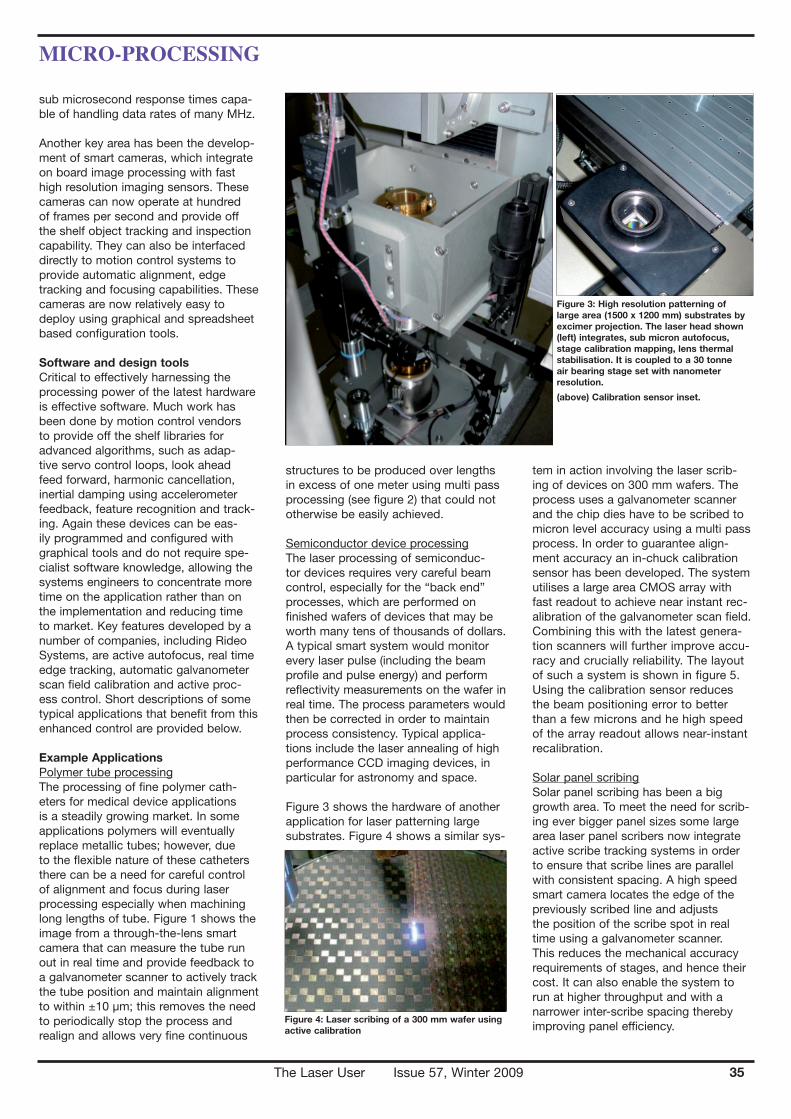
Figure 2: Fine filigree structures machined in 800 um diameter flexible Peek (top) and Polyimide tubes using UV laser multi-pass processing. With active alignment tracking it is possible to process tubes over 1 meter in length. Courtesy Blueacre technology.
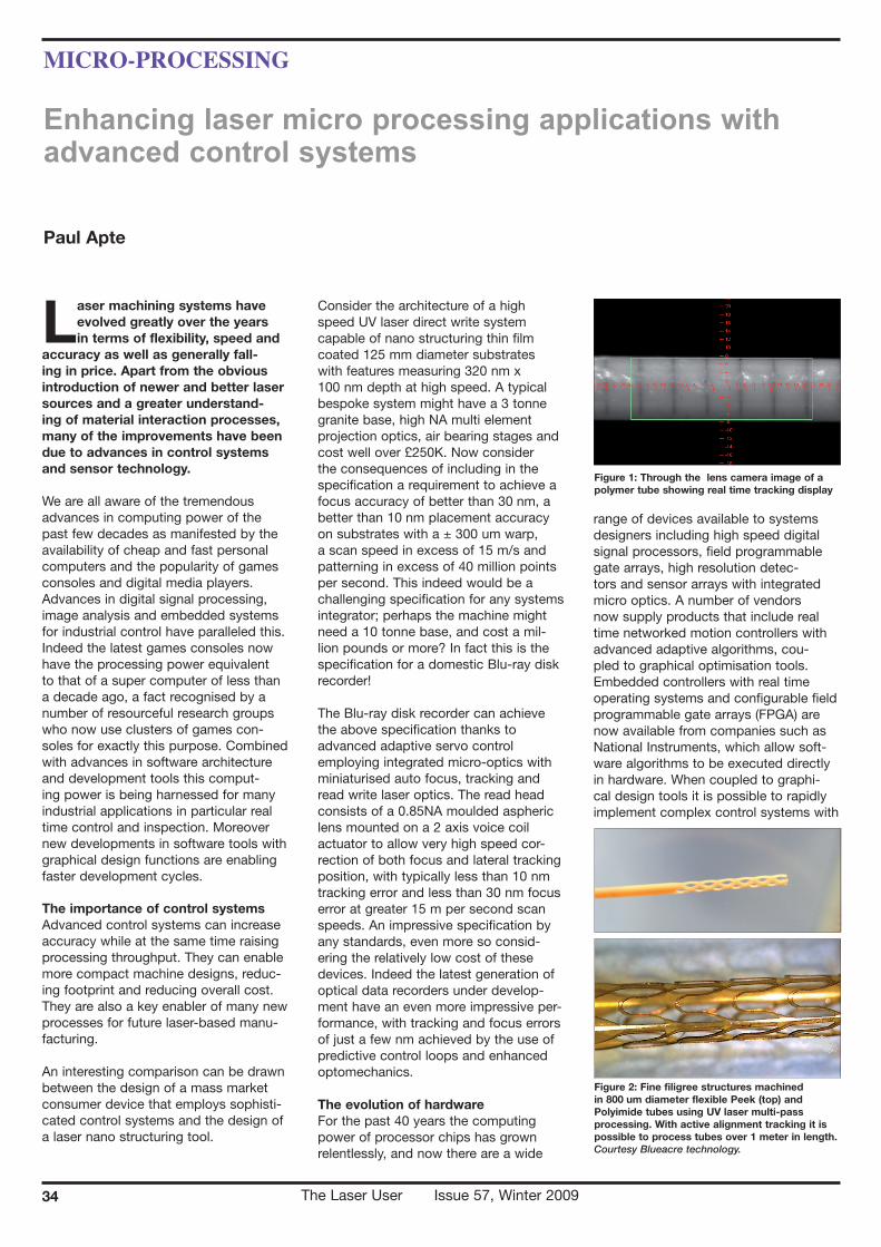
Figure 1: Through the lens camera image of a polymer tube showing real time tracking display
The Laser User Issue 57, Winter 2009
MICRO-PROCESSING
35
sub microsecond response times capa-ble of handling data rates of many MHz.
Another key area has been the develop-ment of smart cameras, which integrate on board image processing with fast high resolution imaging sensors. These cameras can now operate at hundred of frames per second and provide off the shelf object tracking and inspection capability. They can also be interfaced directly to motion control systems to provide automatic alignment, edge tracking and focusing capabilities. These cameras are now relatively easy to deploy using graphical and spreadsheet based configuration tools.
Software and design toolsCritical to effectively harnessing the processing power of the latest hardware is effective software. Much work has been done by motion control vendors to provide off the shelf libraries for advanced algorithms, such as adap-tive servo control loops, look ahead feed forward, harmonic cancellation, inertial damping using accelerometer feedback, feature recognition and track-ing. Again these devices can be eas-ily programmed and configured with graphical tools and do not require spe-cialist software knowledge, allowing the systems engineers to concentrate more time on the application rather than on the implementation and reducing time to market. Key features developed by a number of companies, including Rideo Systems, are active autofocus, real time edge tracking, automatic galvanometer scan field calibration and active proc-ess control. Short descriptions of some typical applications that benefit from this enhanced control are provided below.
Example ApplicationsPolymer tube processingThe processing of fine polymer cath-eters for medical device applications is a steadily growing market. In some applications polymers will eventually replace metallic tubes; however, due to the flexible nature of these catheters there can be a need for careful control of alignment and focus during laser processing especially when machining long lengths of tube. Figure 1 shows the image from a through-the-lens smart camera that can measure the tube run out in real time and provide feedback to a galvanometer scanner to actively track the tube position and maintain alignment to within ±10 µm; this removes the need to periodically stop the process and realign and allows very fine continuous
structures to be produced over lengths in excess of one meter using multi pass processing (see figure 2) that could not otherwise be easily achieved.
Semiconductor device processingThe laser processing of semiconduc-tor devices requires very careful beam control, especially for the “back end” processes, which are performed on finished wafers of devices that may be worth many tens of thousands of dollars. A typical smart system would monitor every laser pulse (including the beam profile and pulse energy) and perform reflectivity measurements on the wafer in real time. The process parameters would then be corrected in order to maintain process consistency. Typical applica-tions include the laser annealing of high performance CCD imaging devices, in particular for astronomy and space.
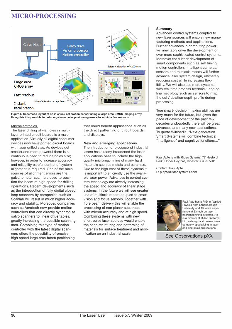
Figure 3 shows the hardware of another application for laser patterning large substrates. Figure 4 shows a similar sys-
tem in action involving the laser scrib-ing of devices on 300 mm wafers. The process uses a galvanometer scanner and the chip dies have to be scribed to micron level accuracy using a multi pass process. In order to guarantee align-ment accuracy an in-chuck calibration sensor has been developed. The system utilises a large area CMOS array with fast readout to achieve near instant rec-alibration of the galvanometer scan field. Combining this with the latest genera-tion scanners will further improve accu-racy and crucially reliability. The layout of such a system is shown in figure 5. Using the calibration sensor reduces the beam positioning error to better than a few microns and he high speed of the array readout allows near-instant recalibration.
Solar panel scribingSolar panel scribing has been a big growth area. To meet the need for scrib-ing ever bigger panel sizes some large area laser panel scribers now integrate active scribe tracking systems in order to ensure that scribe lines are parallel with consistent spacing. A high speed smart camera locates the edge of the previously scribed line and adjusts the position of the scribe spot in real time using a galvanometer scanner. This reduces the mechanical accuracy requirements of stages, and hence their cost. It can also enable the system to run at higher throughput and with a narrower inter-scribe spacing thereby improving panel efficiency.
Figure 4: Laser scribing of a 300 mm wafer using active calibration
Figure 3: High resolution patterning of large area (1500 x 1200 mm) substrates by excimer projection. The laser head shown (left) integrates, sub micron autofocus, stage calibration mapping, lens thermal stabilisation. It is coupled to a 30 tonne air bearing stage set with nanometer resolution.
(above) Calibration sensor inset.
The Laser User Issue 57, Winter 2009
MICRO-PROCESSING
36
Microelectronics The laser drilling of via holes in multi-layer printed circuit boards is a major application. Virtually all digital consumer devices now have printed circuit boards with laser drilled vias. As devices get smaller and more powerful there is a continuous need to reduce holes size; however, in order to increase accuracy and reliability careful control of system alignment is required. One of the main sources of alignment errors are the galvanometer scanners used to posi-tion the beam at high speed for drilling operations. Recent developments such as the introduction of fully digital closed loop scanners by companies such as Scanlab will result in much higher accu-racy and stability. Moreover, companies such as Aerotech now provide motion controllers that can directly synchronise galvo scanners to linear drive tables, greatly increasing the possible scanning area. Combining this type of motion controller with the latest digital scan-ners offers the possibility of precise high speed large area beam positioning
that could benefit applications such as the direct patterning of circuit boards and displays.
New and emerging applicationsThe introduction of picosecond industrial lasers has already broadened the laser applications base to include the high quality micromachining of many hard materials such as metals and ceramics. Due to the high cost of these systems it is important to efficiently use the availa-ble laser power. Advances in control sys-tem technology are already increasing the speed and accuracy of linear stage systems. In the future we will see greater use of multiaxis robots coupled to smart vision and focus sensors. Together with fibre beam delivery this will enable the processing of non planar substrates with micron accuracy and at high speed. Combining these systems with new short pulse laser sources would enable the nano structuring and patterning of materials for surface treatment and mod-ification on an industrial scale.
Summary Advanced control systems coupled to new laser sources will enable new manu-facturing methods and applications. Further advances in computing power will inevitably drive the development of ever more sophisticated control systems. Moreover the further development of smart components such as self tuning motion controllers, intelligent cameras, sensors and multiaxis robots will further advance laser system design, ultimately reducing cost while increasing flex-ibility. We will also see more systems with real time process feedback, and on line metrology such as sensors to map the cut / ablation depth profile during processing.
True smart- decision making abilities are very much for the future, but given the pace of development of the past few decades undoubtedly there will be great advances and many new applications. To quote Wikipedia: “Next generation Smart Systems will combine technical “intelligence” and cognitive functions…”
Paul Apte is with Rideo Sytems, 77 Heyford Park, Upper Heyford, Bicester OX25 5HD
Contact: Paul Apte E: [email protected]
See Observations pXX
Paul Apte has a PhD in Applied Physics from Loughborough University and 15 years expe-rience at Exitech on laser micromachining systems. He is a director at Rideo Systems Ltd, a design and development company specialising in laser and photonics applications.
Figure 5: Schematic layout of an in chuck calibration sensor using a large area CMOS imaging array. Using this it is possible to reduce galvanometer positioning errors to within a few microns