ENHANCED SERIAL AUDIO INTERFACE (ESAI) · Enhanced Serial Audio Interface (ESAI) peripheral...
56
Revision 1.0 Published 05/00 AN1848/D (Motorola Order Number) ENHANCED SERIAL AUDIO INTERFACE (ESAI) Programming and Interfacing Techniques Application Note By: Brent Karley Freescale Semiconductor, I Freescale Semiconductor, Inc. For More Information On This Product, Go to: www.freescale.com nc... Freescale Semiconductor © Freescale Semiconductor, Inc., 2004. All rights reserved.
Transcript of ENHANCED SERIAL AUDIO INTERFACE (ESAI) · Enhanced Serial Audio Interface (ESAI) peripheral...

F
ree
sca
le S
em
ico
nd
uc
tor,
I
Freescale Semiconductor, Inc.n
c..
.
Freescale Semiconductor
© Free
Revision 1.0Published 05/00
AN1848/D(Motorola Order Number)
ENHANCED SERIALAUDIO INTERFACE (ESAI)
Programming and InterfacingTechniques
Application Note
By: Brent Karley
scale Semiconductor, Inc., 2004. All rights reserved.
For More Information On This Product,
Go to: www.freescale.com
F
ree
sca
le S
em
ico
nd
uc
tor,
I
Freescale Semiconductor, Inc.n
c..
.
For More Information On This Product,
Go to: www.freescale.com
rxzb30
disclaimer
rxzb30
freescalecolorjpeg
rxzb30
hibbertleft

Introduction to the ESAI
ESAI Overview
ome
th
nced sors l
as the
F
ree
sca
le S
em
ico
nd
uc
tor,
I
Freescale Semiconductor, Inc.n
c..
.
SECTION 1
INTRODUCTION TO THE ESAI
Interfacing external components to Motorola Digital Signal Processors (DSPs) using the Enhanced Serial Audio Interface (ESAI) peripheral involves both hardware and software coordination. Implementing proper methods and techniques provides considerable system enhancements over conventional serial peripherals. Applications such as DVD, HDTV, set-top box, as well as portable audio and A/V applications such as home theater, can utilize the ESAI to enhance system functionality, reduce system cost, and simultaneously simplify design implementations.
This application note provides a tutorial on utilizing the ESAI peripheral including several hardware and software examples. This application note is recommended for developers with solid programming knowledge and a basic understanding of IC interfacing.
• This section provides an overview of the ESAI peripheral pins and application considerations.
• Section 2, describes hardware interfacing to external components.
• Section 3, contains several hardware interfacing examples using the ESAI with sof the most common peripheral components.
• Section 4, describes common audio data transfer protocols.
• Section 5, provides an overview of how to program the ESAI control registers wiexamples for I2S, Left Justified, and EIAJ protocols.
• Section 6, provides an ESAI programming example.
1.1 ESAI OVERVIEW
The Enhanced Serial Audio Interface (ESAI) is an integration of the multi-capable EnhaSynchronous Serial Interface (ESSI) common to many of Motorola’s DSP56300 procesand the Serial Audio Interface (SAI) designed specifically for consumer and professionaaudio applications on Motorola’s first generation of dedicated audio processors known SymphonyTM family.
ESAI Programming and Interfacing Techniques 1-1 For More Information On This Product,
Go to: www.freescale.com

Introduction to the ESAI
ESAI Structure
tware
t erate
, six
ith the d in
F
ree
sca
le S
em
ico
nd
uc
tor,
I
Freescale Semiconductor, Inc.n
c..
.
The ESAI provides for simple interfacing to common audio Analog-to-Digital converters (ADC) and Digital-to-Analog converters (DACs) which utilize the I2S interfacing protocol. The ESAI provides several advanced audio peripheral capabilities such as:
• Flexibility in the number of inputs and outputs supported
• Over sample clocking support
• Hardware driven multiplexing
• Right justified (EIAJ) support
• AC-97 capabilities
This application note describes how to utilize these features (except for AC-97 which iscovered in application note APR37) with examples of both hardware interfacing and sofprogramming.
1.2 ESAI STRUCTURE
The ESAI is divided into separate receiver and transmitter sections with independent biclocks, framesync clocks, and over sample clocks. The ESAI can be programmed to opthe transmitter and receiver sections in the following ways:
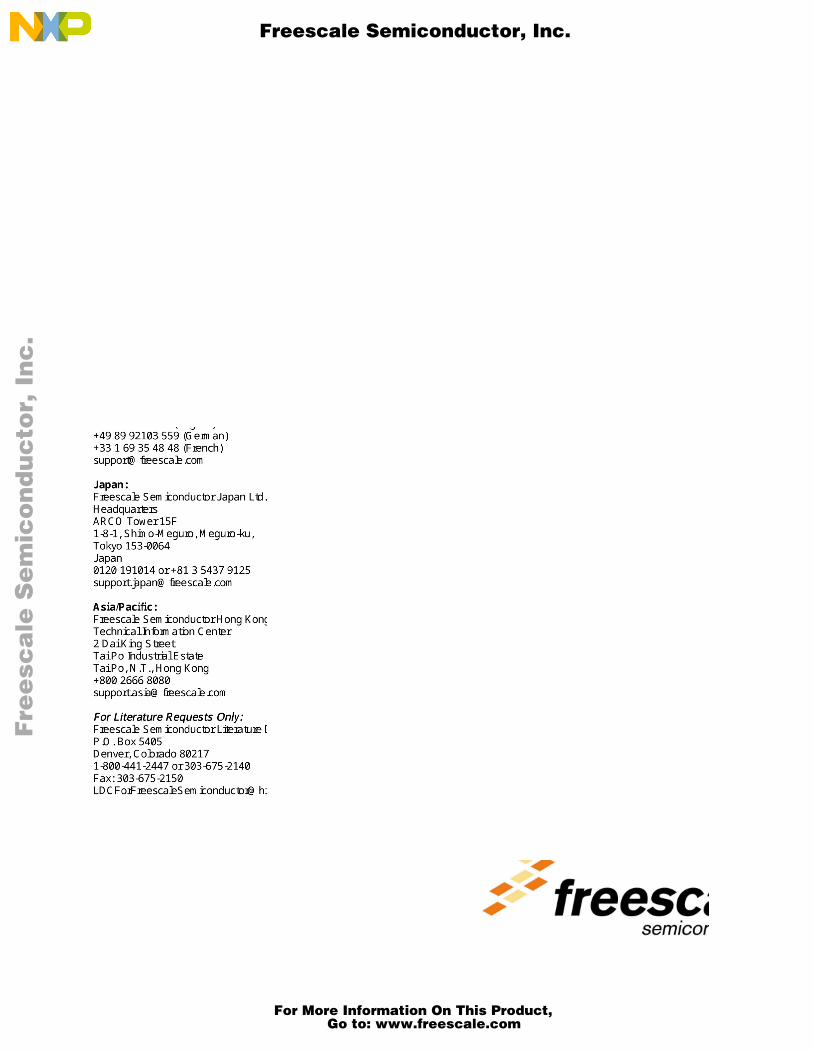
The number of I/O pins may vary depending upon the particular DSP utilized. Typicallydata I/O pins are available, two of which are dedicated outputs and four of which are programmable as either input or output. Figure 1-1 shows each of the pins associated wESAI peripheral as implemented on the DSP56362. A description of each pin is provideTable 1-2, “Audio Data I/O Pin Function,” on page 1-3.
Table 1-1 Transmitter and Receiver Section Programming
Mode Description
synchronous Receiver and transmitter using the same clock source
asynchronous Receiver and transmitter using different clock sources
master Clocks generated by the DSP core
slave Clocks provided externally
ESAI Programming and Interfacing Techniques 1-2 For More Information On This Product,
Go to: www.freescale.com
Introduction to the ESAI
ESAI Structure
F
ree
sca
le S
em
ico
nd
uc
tor,
I
Freescale Semiconductor, Inc.n
c..
.
Figure 1-1 ESAI Pins
1.2.1 ESAI PIN DESCRIPTION
The following table describes how each pin transfers audio data in and out of the DSP.
Table 1-2 Audio Data I/O Pin Function
Pin Name Pin Description
SCKR The receive bit clock is utilized to clock in each bit of audio data received by the DSP. The receive bit clock signal can either be generated by the DSP (master mode) or generated externally (slave mode).
FSR The receive framesync clock is utilized to clock in each audio sample received by the DSP. The receive framesync clock signal can either be generated by the DSP (master mode) or generated externally (slave mode).
HCKR The receive over sample clock is not necessary for operation by the DSP but is convenient for generating the bit clock (SCKR) and framesync clock (FSR). The receive over sample clock signal can either be generated by the DSP (master mode) or generated externally (slave mode).
SCKT The transmit bit clock is utilized to clock out each bit of audio data transmitted by the DSP. The transmit bit clock signal can either be generated by the DSP (master mode) or generated externally (slave mode).
FST The transmit framesync clock is utilized to clock out each audio sample transmitted by the DSP. The transmit framesync clock signal can either be generated by the DSP (master mode) or generated externally (slave mode).
HCKT The transmit over sample clock is not necessary for operation by the DSP but is convenient for generating the bit clock (SCKT) and framesync clock (FST). The transmit over sample clock signal can either be generated by the DSP (master mode) or generated externally (slave mode).
SDO5/SDI0 The SDO5/SDI0 data pin can be programmed as either a transmitter (SDO5) or as a receiver (SDI0). When operating as a transmitter this pin operates in conjunction with the transmit clocks (SCKT, FST, HCKT) to transmit data out of the DSP. When operating as a receiver this pin operates in conjunction with the receiver clocks (SCKR, FSR, HCKR) to receive data into the DSP.
EnhancedSerialAudio
Interface(ESAI)
SCKRFSRHCKR
SDO5/SDI0SDO4/SDI1SDO3/SDI2SDO2/SDI3
SCKTFSTHCKTSDO1SDO0
MotorolaDSP56362
Threededicated
Receiver Pins
FourProgrammable I/O
Pins
FiveDedicated
TransmitterPins
ESAI Programming and Interfacing Techniques 1-3 For More Information On This Product,
Go to: www.freescale.com

Introduction to the ESAI
ESAI Structure
F
ree
sca
le S
em
ico
nd
uc
tor,
I
Freescale Semiconductor, Inc.n
c..
.
1.2.2 ESAI PIN CONFIGURATIONS
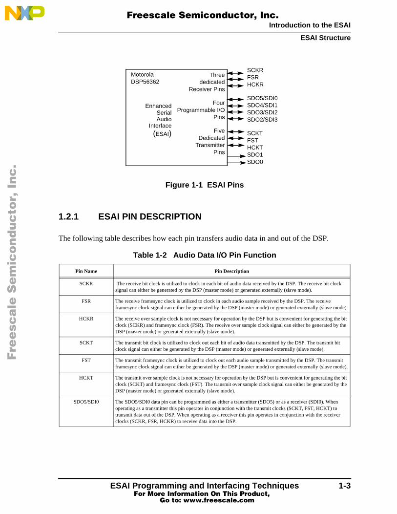
Table 1-3 shows the possible ESAI input/output combinations given six data I/O pins. Each input and output pin can be programmed to carry from one to thirty-two data slots. Each slot can be used to carry an audio sample.
Typically, the ESAI is programmed for two slots (left channel, right channel) as shown in Figure 1-2. Section 4, Digital Audio Transfer Protocols, describes common audio transfer protocols which utilize this two slot concept.
SDO4/SDI1 The SDO4/SDI1 data pin can be programmed as either a transmitter (SDO4) or as a receiver (SDI1). When operating as a transmitter this pin operates in conjunction with the transmit clocks (SCKT, FST, HCKT) to transmit data out of the DSP. When operating as a receiver this pin operates in conjunction with the receiver clocks (SCKR, FSR, HCKR) to receive data into the DSP.
SDO3/SDI2 The SDO3/SDI2 data pin can be programmed as either a transmitter (SDO3) or as a receiver (SDI2). When operating as a transmitter this pin operates in conjunction with the transmit clocks (SCKT, FST, HCKT) to transmit data out of the DSP. When operating as a receiver this pin operates in conjunction with the receiver clocks (SCKR, FSR, HCKR) to receive data into the DSP.
SDO2/SDI3 The SDO2/SDI3 data pin can be programmed as either a transmitter (SDO2) or as a receiver (SDI3). When operating as a transmitter this pin operates in conjunction with the transmit clocks (SCKT, FST, HCKT) to transmit data out of the DSP. When operating as a receiver this pin operates in conjunction with the receiver clocks (SCKR, FSR, HCKR) to receive data into the DSP.
SDO1 The SDO1 data pin operates only as a transmitter pin in conjunction with the transmitter clocks.
SDO0 The SDO0 data pin operates only as a transmitter pin in conjunction with the transmitter clocks.
Table 1-3 ESAI Input/Output Configurations
Configuration Input Pins Output Pins
1 0 6
2 1 5
3 2 4
4 3 3
5 4 2
Table 1-2 Audio Data I/O Pin Function
Pin Name Pin Description
ESAI Programming and Interfacing Techniques 1-4 For More Information On This Product,
Go to: www.freescale.com
Introduction to the ESAI
Application Considerations
d ch as:
els ed on tputs
nsmit
F
ree
sca
le S
em
ico
nd
uc
tor,
I
Freescale Semiconductor, Inc.n
c..
.
Figure 1-2 Data Transfer over ESAI
1.3 APPLICATION CONSIDERATIONS
The ESAI is efficient for applications that implement multichannel processing. Applications such as cinema processing and home theater typically implement decompression algorithms (i.e. Dolby Digital, DTS, MPEG, Pro Logic, etc...) that can take advantage of the many I/O features in the ESAI. The ESAI’s multiple I/Os and flexible protocol support make it a goofit for these applications. However, because the ESAI is a versatile peripheral, there areseveral system level questions to consider regarding how to best implement the ESAI su
• How many input and output channels are required for the system?
• What type of hardware interface is required to support the external components?
• What data transfer protocols do the external components support?
• What are the clocking requirements for the external components?
1.3.1 INPUT AND OUTPUT CHANNELS
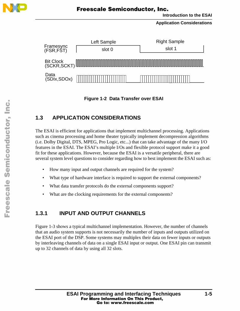
Figure 1-3 shows a typical multichannel implementation. However, the number of channthat an audio system supports is not necessarily the number of inputs and outputs utilizthe ESAI port of the DSP. Some systems may multiplex their data on fewer inputs or ouby interleaving channels of data on a single ESAI input or output. One ESAI pin can traup to 32 channels of data by using all 32 slots.
Framesync
Bit Clock
Data
(SCKR,SCKT)
(FSR,FST)
(SDIx,SDOx)
slot 0 slot 1Left Sample Right Sample
ESAI Programming and Interfacing Techniques 1-5 For More Information On This Product,
Go to: www.freescale.com
Introduction to the ESAI
Application Considerations
F
ree
sca
le S
em
ico
nd
uc
tor,
I
Freescale Semiconductor, Inc.n
c..
.
Figure 1-3 Multichannel Processor I/O Block Diagram
1.3.2 HARDWARE INTERFACE
Hardware interface requirements can vary depending upon the specific type of converter and other peripheral components in the system. Most audio components support a three line transmission interface consisting of a:
1. Data line
2. Bit clock
3. Framesync clock
Not all audio components support a three line interface. Some components also require a high frequency over sampled clock. Another hardware interface variation is required for mono ADCs and DACs. For example, many high end mono converters such as the Burr Brown PCM63 utilize a data latch rather than a framesync and thus receive only one channel of data.
1.3.3 TRANSFER PROTOCOL
The ESAI supports multiple I/O protocols, even those protocols which are not necessarily common to audio components. The type of protocol utilized should be matched with the protocols supported by external components in the audio system. The most common audio protocols are I2S, left justified, and EIAJ (right justified) formats. However, as described in
Motorola DSP563xxESAI
DAC
ADC
SPDIF RX
DAC
DAC
Left
Right
Center
Subwoofer
Left Surround
Right Surround
Left
Right
Digital input
Left Auxiliary
Right Auxiliary
SPDIF TX
SDI1
SDI0 SDO0
SDO1
SDO2
SDO3
ESAI Programming and Interfacing Techniques 1-6 For More Information On This Product,
Go to: www.freescale.com
Introduction to the ESAI
Application Considerations
F
ree
sca
le S
em
ico
nd
uc
tor,
I
Freescale Semiconductor, Inc.n
c..
.
the previous section, mono converters may utilize a unique hardware interface and transfer protocol. Some components utilize multiplexed data across a single input or output or may demand a high frequency over sampled clock.
1.3.4 CLOCKING REQUIREMENTS
Some audio components have the ability to generate system clocks and operate in master mode while others can only operate in slave mode receiving clocks from other system components. The clocking requirements of any system must be considered when determining which components to use. Jitter specifications must also be met to gain maximum quality from system components. These clocking considerations are described in more detail in Hardware Handling and Layout Considerations on page 2 - 5.
ESAI Programming and Interfacing Techniques 1-7 For More Information On This Product,
Go to: www.freescale.com
Introduction to the ESAI
Application Considerations
F
ree
sca
le S
em
ico
nd
uc
tor,
I
Freescale Semiconductor, Inc.n
c..
.
1-8 AI Programming and Interfacing Techniques MOTOROLA For More Information On This Product,
Go to: www.freescale.com

ESAI Hardware Design Considerations
Interfacing the ESAI to External Components
F
ree
sca
le S
em
ico
nd
uc
tor,
I
Freescale Semiconductor, Inc.n
c..
.
SECTION 2
ESAI HARDWARE DESIGN CONSIDERATIONS
The ESAI peripheral is designed to easily interface with all conventional audio peripherals as well as various atypical audio components. This section describes the hardware interfacing items as they relate to operating the ESAI with external audio components.
2.1 INTERFACING THE ESAI TO EXTERNAL COMPONENTS
Interfacing the ESAI receiver or transmitter to peripheral components requires three pin connections. For each of the receiver and transmitter sections there are the following pin connections:
1. Bit clock (SCKR, SCKT) — Clocks the data bits of every sample in or out
2. Framesync clock (FSR, FST) — Clocks each sample in or out.
3. Various data (SDIx, SDOx) pins — Carries the audio information.
Figure 2-1 shows a timing diagram for a typical ESAI audio sample transfer.
Figure 2-1 ESAI Timing Diagram
Framesync
Bit Clock
Data
New Sample New Sample
(SCKR,SCKT)
(FSR,FST)
(SDIx,SDOx)
Left Frame Right Frame
Audio Data
23 0 23 0
New Sample
ESAI Programming and Interface Techniqes 2-1 For More Information On This Product,
Go to: www.freescale.com

ESAI Hardware Design Considerations
ESAI Clocking Examples
r clock es a
e er ck
F
ree
sca
le S
em
ico
nd
uc
tor,
I
Freescale Semiconductor, Inc.n
c..
.
2.2 ESAI CLOCKING EXAMPLES
This section describes several common clocking schemes and addresses clocking issues and considerations. Four examples are provided that cover the most common ESAI clocking implementations.
2.2.1 ADC — DSP — DAC INTERFACE
Figure 2-2 shows both the ESAI receiver and transmitter operating in slave mode as the clocks are being provided externally from the ADC. The ADC utilizes an external clock oscillator as its over sampled clock source. This design is typical of A/V receivers and portable applications that receive only analog signals utilizing sigma-delta converters. Sigma-delta converters require an over sampled clock. Phase jitter and clock noise are common problems that affect sigma-delta converters which reduces the quality of a converter’s output. Most converters can tolerate some jitter and continue to operate. However, excessive jitter odrift reduces signal quality or causes catastrophic failures. This clocking scheme providhigh quality conversion.
Providing all clocks from a single over sampled source, such as a low jitter crystal, is onmethod of reducing jitter in the audio system. Typically, ADCs are provided a master ovsampled clock (i.e. 256fs, 384fs or 512fs) and generate the bit clock and framesync clowhich is distributed to both the DSP and DAC.
Figure 2-2 ADC - DSP - ADC Interface
FST
SCKT
SDO0
FSR
SCKR
SDI0
MCLKL
RCK
BCLK
SDO
MCLK
LRCK
BCLK
SDI
ADC DACDSP563xx
ESAI Programming and Interface Techniqes 2-2 For More Information On This Product,
Go to: www.freescale.com

ESAI Hardware Design Considerations
ESAI Clocking Examples
F
ree
sca
le S
em
ico
nd
uc
tor,
I
Freescale Semiconductor, Inc.n
c..
.
2.2.2 DSP — S/PDIF INTERFACE
The S/PDIF receiver is a unique component in that the bit clock and framesync clock must be derived directly from the input signal of the S/PDIF receiver. The S/PDIF input signal carries both data and clock information. As shown in Figure 2-3, the bit clock and frame sync clock are generated from the S/PDIF receiver and drive both the receiver and transmitter of the DSP as well as the S/PDIF transmitter. This design is common in A/V receivers that receive and transmit digital audio data to and from external components. This design is susceptible to jitter associated with the PLL of the SPDIF receiver as well as clock drift or clock freeze when the external SPDIF signal is interrupted.
Figure 2-3 DSP - S/DPIF Interface
FST
SCKT
SDO0
FSR
SCKR
SDI0
LRCK
BCLK
SDO
LRCK
BCLK
SDI
S/PDIF RCVRS/PDIF XMTRDSP563xx
ESAI Programming and Interface Techniqes 2-3 For More Information On This Product,
Go to: www.freescale.com
ESAI Hardware Design Considerations
ESAI Clocking Examples
F
ree
sca
le S
em
ico
nd
uc
tor,
I
Freescale Semiconductor, Inc.n
c..
.
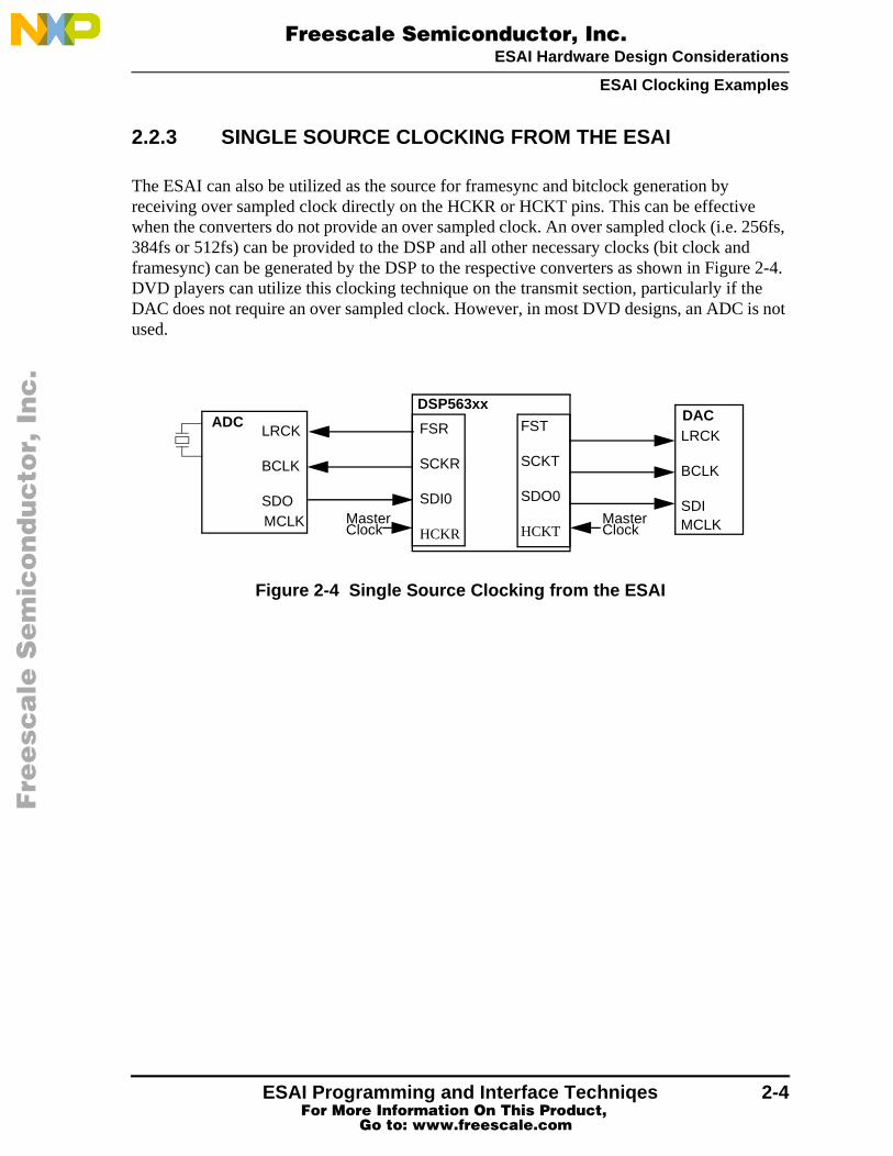
2.2.3 SINGLE SOURCE CLOCKING FROM THE ESAI
The ESAI can also be utilized as the source for framesync and bitclock generation by receiving over sampled clock directly on the HCKR or HCKT pins. This can be effective when the converters do not provide an over sampled clock. An over sampled clock (i.e. 256fs, 384fs or 512fs) can be provided to the DSP and all other necessary clocks (bit clock and framesync) can be generated by the DSP to the respective converters as shown in Figure 2-4. DVD players can utilize this clocking technique on the transmit section, particularly if the DAC does not require an over sampled clock. However, in most DVD designs, an ADC is not used.
Figure 2-4 Single Source Clocking from the ESAI
FST
SCKT
SDO0
HCKT
FSR
SCKR
SDI0
HCKR
LRCK
BCLK
SDO
LRCK
BCLK
SDI
ADC DACDSP563xx
MCLKMCLK MasterClock
MasterClock
ESAI Programming and Interface Techniqes 2-4 For More Information On This Product,
Go to: www.freescale.com

ESAI Hardware Design Considerations
Hardware Handling and Layout Considerations
F
ree
sca
le S
em
ico
nd
uc
tor,
I
Freescale Semiconductor, Inc.n
c..
.
2.2.4 ESAI MASTER MODE
The DSP can also operate in master mode with all clocks generated from the internal oscillator of the DSP. This requires the internal oscillator to operate at a frequency which is a multiple of the over sampled clock. In this example, the over sampled clock drives the DSP using the EXTAL pin. The on-chip PLL multiplies up the external over sample clock provided to the EXTAL pin to a reasonable internal operating frequency (fosc). The ESAI can be programmed to divide down the internal oscillator clock (fosc) to provide the over sampled clocks, framesync clocks, and bit clocks for the receiver and/or transmitter. This method is used in applications where the external components are not capable of sourcing I/O clocks. This design can result in reduced audio quality due to the potential for excessive clock jitter in the DSP PLL. See Figure 2-5.
Figure 2-5 ESAI Master Mode
2.3 HARDWARE HANDLING AND LAYOUT CONSIDERATIONS
Failure to observe proper handling and installation procedures can cause damage to the ESAI. The ESAI can be damaged by Electrostatic Discharge (ESD), so it is recommended that all DSPs be handled with appropriate precautions. ESD damage ranges from subtle performance degradation to complete peripheral failure.
The ESAI is powered by two Vccs which must be tied to all other DSP power inputs. When multiple ESAI peripherals exist on a single DSP, the ESAI Vcc pins should be tied to all other Vcc pins. Adequate decoupling must be provided via external capacitors. Two ground pins (GNDs) are also provided which must be tied to all other DSP ground connections.
FST
SCKT
SDO0
HCKT
FSR
SCKR
SDI0
HCKR
EXTAL
LRCK
BCLK
SDO
ADCDACDSP563xx
MCLKMCLK
MasterClock
LRCK
BCLK
SDI
ESAI Programming and Interface Techniqes 2-5 For More Information On This Product,
Go to: www.freescale.com

ESAI Hardware Design Considerations
Hardware Handling and Layout Considerations
ngth
es
F
ree
sca
le S
em
ico
nd
uc
tor,
I
Freescale Semiconductor, Inc.n
c..
.
Ensure that each of the following guidelines are followed:
• All board traces for the ESAI clocks and data should be less than six inches in leto provide for robust clock and data signals.
• Adequately separate the digital and analog signals to reduce signal interference.
• Properly ground the analog section of converters as recommended by the manufacturer in order to minimize digital clock noise in the analog ground plane.Refer to the converter’s data sheet for details regarding grounding.
• Analog board traces should be as short as possible to reduce the effects of electromagnetic Interference (EMI) which can be generated by a variety of sourcincluding high speed clocks and data.
2-6 AI Programming and Interface Techniqes MOTOROLA For More Information On This Product,
Go to: www.freescale.com

ESAI Interfacing Examples
Introduction
ation
trol ty of s
F
ree
sca
le S
em
ico
nd
uc
tor,
I
Freescale Semiconductor, Inc.n
c..
.
SECTION 3
ESAI INTERFACING EXAMPLES
3.1 INTRODUCTION
This section provides three examples of interfacing the ESAI to common peripheral components from Asahi Kasei Microsystems (AKM), Burr Brown, and Crystal Semiconductor. Each example is unique in features and implementation and represents the most common designs for audio/video systems. A description of the capabilities of each system, their external components, ESAI interface, clocking scheme, and supported transfer protocols is provided.
3.2 INTERFACING TO AKM COMPONENTS
Figure 3-1 shows an audio system consisting of AKM components and the Motorola DSP56362. This design can be utilized in a variety of applications including portable audio designs, mini-systems, and A/V receivers.
3.2.1 AKM COMPONENT OVERVIEW
This design implements an audio system consisting of a Motorola DSP56362 and the following AKM components:
• AK4112 Digital Audio Receiver
• AK4526 CODEC
• AK5353 ADC
Refer to the respective AKM data sheets for information regarding additional implementrequirements and control information.
The AK4112 is a high performance single chip AES/EBU-S/PDIF digital audio receiver supporting up to 24 bit, 96 kHz data. Four selectable inputs are available with input conusing either serial or parallel interfaces. This allows the AK4112 to interface with a variemicro controllers. The AK4112 supports both consumer and professional channel statu
ESAI Programming and Interface Techniqes 3-1 For More Information On This Product,
Go to: www.freescale.com
ESAI Interfacing Examples
Interfacing to AKM Components
F
ree
sca
le S
em
ico
nd
uc
tor,
I
Freescale Semiconductor, Inc.n
c..
.
modes and can automatically detect AC-3 and MPEG bitstreams. Support for digital audio protocols including AES/EBU, IEC958, S/PDIF, and EIAJ CP1201 is provided.
The AK4526 is a high performance single chip CODEC that includes two channels of 96 kHz, 20-bit ADC and six channels of 96 kHz, 24-bit DAC. The AK4526 also supports an auxiliary digital input. The following example uses the auxiliary digital input to receive the AK4112 digital output. This system can input data from either the AK4526 ADC or the SPDIF receiver, but not both at the same time. This system design minimizes the number of ESAI data pins required for data input.
The AK5353 is a single chip 48 kHz, 20 bit ADC which, in this example, serves as a secondary input for applications such as karaoke.
3.2.2 SYSTEM OVERVIEW
This design provides four digital AES/EBU-S/PDIF inputs using the AK4112 and two stereo analog inputs (one stereo input on the AK4526 and one stereo input on the AK5353). Only one of the four digital inputs or the analog input on the AK4526 can be used at any given time. However, the analog input from the AK5353 can be used at any time. There are six analog output channels available using the AK4526. This system supports sample rates of 32 kHz, 44.1 kHz, 48 kHz, or 96 kHz.
In a mini-system or A/V receiver, this system supports multiple digital audio input sources (i.e. DVD, VCR, Set top box, CD) and with the addition of an input switcher can support multiple analog inputs (i.e. tuner, CD, tape decks, VCR, DVD, etc...). A secondary stereo analog input can be supported for functions such as karaoke. The DSP can be used in this system to perform several digital audio functions including decoding Dolby Digital, DTS, MPEG, and Dolby Pro Logic processing, as well as supporting features such as equalization, tone/balance control, volume control, karaoke processes, or soundfield processing (i.e. Hall effects).
3.2.3 IMPLEMENTATION
3.2.3.1 Data InterfaceThe four digital audio inputs are provided using the AK4112 at inputs RX1, RX2, RX3, and RX4. The AK4112 selects one of the four inputs to send to the AK4526 using the SDTO pin. Stereo analog inputs are available at the AINL and AINR inputs of the AK4526. The AK4526 selects either the digital audio signal from the AK4112 or the analog signal to send to the DSP using the SDTO pin. Only one of the two can be sent to the DSP. This signal is received by the ESAI peripheral of the DSP at pin SDI1. The secondary stereo analog input is available at the
ESAI Programming and Interface Techniqes 3-2 For More Information On This Product,
Go to: www.freescale.com

ESAI Interfacing Examples
Interfacing to AKM Components
F
ree
sca
le S
em
ico
nd
uc
tor,
I
Freescale Semiconductor, Inc.n
c..
.
AINL and AINR inputs of the AK5353. The digital output is provided at the SDTO pin and interfaces to the ESAI peripheral of the DSP at pin SDI0.
The DSP processes the data provided from both the AK4526 and the AK5353 and outputs six channels of digital data using the ESAI transmit pins (SDO0, SDO1 and SDO2) to the AK4526 digital input section (SDI1, SDI2, and SDI3). The six channels of digital data is converted to analog signals by the AK4526 and output using the pins LOUT1, ROUT1, LOUT2, ROUT2, LOUT3, and ROUT3.
All components in this system operate using 3.3V power sources with matching input, output, and clock levels.
3.2.3.2 System ClockingThe master clock of this system is provided by the AK4112 at pins MCK01 and MCK02. Clocks are generated from the digital input which carries both clock and data information. When there are no digital signals available, the AK4112 utilizes the external clock source to generate the system clocks. A low jitter PLL supporting up to 96 KHz operation on the AK4112 generates the system bitclock (BICK) and framesync clock (LRCK) and passes the master clock (MCK01) to the rest of the system. Providing clocks from a single low jitter source minimizes signal degradation and guarantees the most robust signals. This type of low jitter clocking results in the highest quality audio signal path. All components operate in slave mode except the AK4112 which operates in master mode and generates all system clocks.
Figure 3-1 AKM / DSP56362 Digital Audio System Example
Clock
FSRSCKR
SDI0
FSTSCKT
SDO0SDO1SDO2
AK4112
DSP56362
AK5353
AK4526
ROUT3LOUT3ROUT2LOUT2ROUT1LOUT1
XTIMCKO2
MCKO1
MCLKSDI1
SCLKLRCLKSDTO
SDTO
LRCKBICK
MCLIAAUX
SDI3SDI2SDI1LRCKBICK
SDTO
AINLAINR
AINL
AINR
RX1
RX2
RX3
RX4
DataClock
Source
ESAI Programming and Interface Techniqes 3-3 For More Information On This Product,
Go to: www.freescale.com
ESAI Interfacing Examples
Interfacing to Burr Brown Components
Hz
alog 1716
er, input econd digital as
h the
F
ree
sca
le S
em
ico
nd
uc
tor,
I
Freescale Semiconductor, Inc.n
c..
.
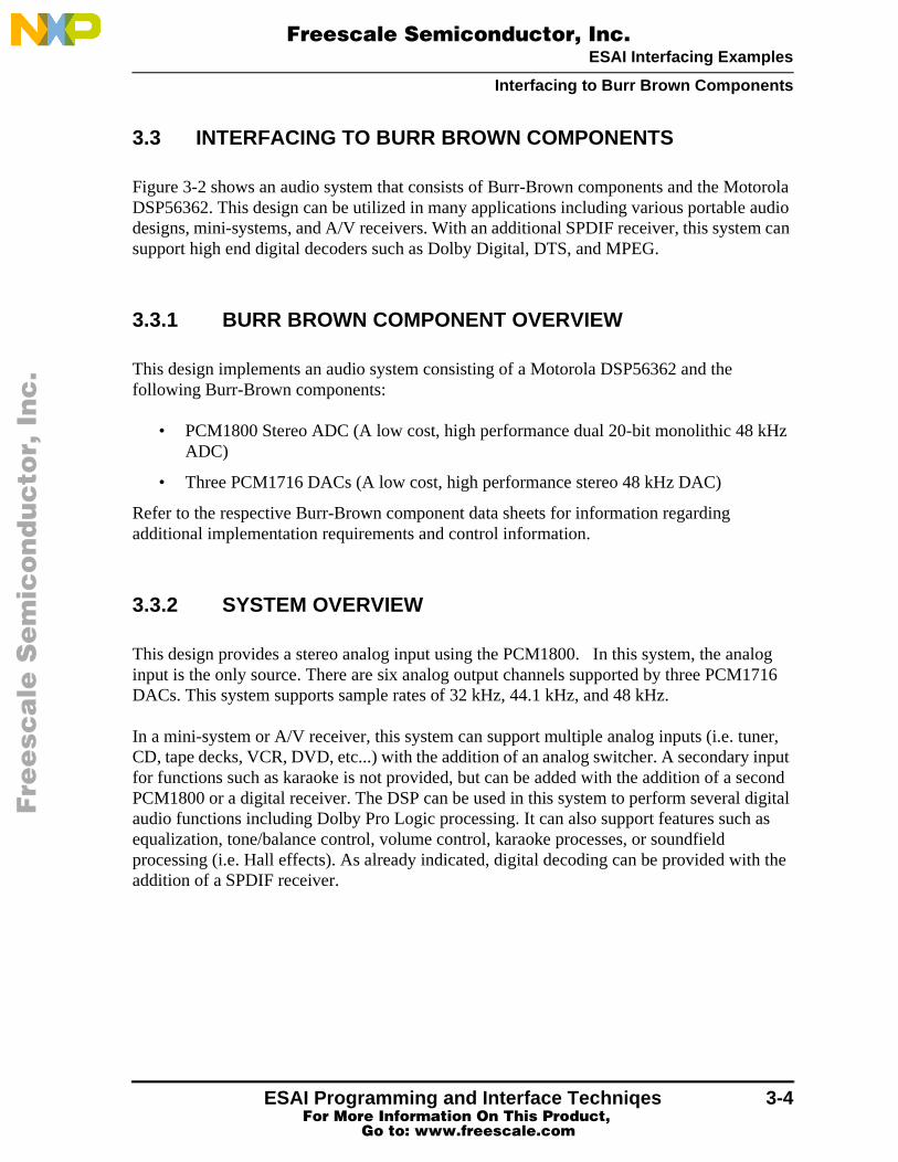
3.3 INTERFACING TO BURR BROWN COMPONENTS
Figure 3-2 shows an audio system that consists of Burr-Brown components and the Motorola DSP56362. This design can be utilized in many applications including various portable audio designs, mini-systems, and A/V receivers. With an additional SPDIF receiver, this system can support high end digital decoders such as Dolby Digital, DTS, and MPEG.
3.3.1 BURR BROWN COMPONENT OVERVIEW
This design implements an audio system consisting of a Motorola DSP56362 and the following Burr-Brown components:
• PCM1800 Stereo ADC (A low cost, high performance dual 20-bit monolithic 48 kADC)
• Three PCM1716 DACs (A low cost, high performance stereo 48 kHz DAC)
Refer to the respective Burr-Brown component data sheets for information regarding additional implementation requirements and control information.
3.3.2 SYSTEM OVERVIEW
This design provides a stereo analog input using the PCM1800. In this system, the aninput is the only source. There are six analog output channels supported by three PCMDACs. This system supports sample rates of 32 kHz, 44.1 kHz, and 48 kHz.
In a mini-system or A/V receiver, this system can support multiple analog inputs (i.e. tunCD, tape decks, VCR, DVD, etc...) with the addition of an analog switcher. A secondary for functions such as karaoke is not provided, but can be added with the addition of a sPCM1800 or a digital receiver. The DSP can be used in this system to perform several audio functions including Dolby Pro Logic processing. It can also support features suchequalization, tone/balance control, volume control, karaoke processes, or soundfield processing (i.e. Hall effects). As already indicated, digital decoding can be provided witaddition of a SPDIF receiver.
ESAI Programming and Interface Techniqes 3-4 For More Information On This Product,
Go to: www.freescale.com

ESAI Interfacing Examples
Interfacing to Burr Brown Components
F
ree
sca
le S
em
ico
nd
uc
tor,
I
Freescale Semiconductor, Inc.n
c..
.
3.3.3 IMPLEMENTATION
3.3.3.1 Data InterfaceStereo analog inputs are available at the VINL and VINR inputs of the PCM1800. The PCM1800 sends digital data to the DSP using the DOUT pin. This signal is received by the ESAI peripheral of the DSP at pin SDI0.
The DSP processes the data provided from the PCM1800 and outputs six channels of digital data using ESAI transmit pins (SDO0, SDO1 and SDO2) to the three PCM1716s digital input section at the DIN pin. The six channels of digital data is converted to analog signals by the PCM1716s and output using the pins VOUTL and VOUTR.
All Burr-Brown components in this system operate using 5.0 V power sources while the DSP56362 is supported with 3.3. V power sources. The DSP56362 ESAI is 5.0 V tolerant and can support the levels required by the Burr-Brown components.
3.3.3.2 System ClockingThe system clocks are provided by the PCM1800 and are generated using the external clock source shown in Figure 3-2. A low jitter PLL that supports up to 48 KHz operation on the PCM1800 generates the system bitclock (BCK) and framesync clock (LRCK). Providing clocks from a single low jitter source minimizes signal degradation and guarantees the most robust signals. This type of low jitter clocking results in the highest quality audio signal path. All components operate in slave mode except the PCM1800 which operates in master mode and generates all system clocks.
ESAI Programming and Interface Techniqes 3-5 For More Information On This Product,
Go to: www.freescale.com
ESAI Interfacing Examples
Interfacing to Crystal Semiconductor Components
F
ree
sca
le S
em
ico
nd
uc
tor,
I
Freescale Semiconductor, Inc.n
c..
.
Figure 3-2 Burr-Brown / DSP56362 Digital Audio System Example
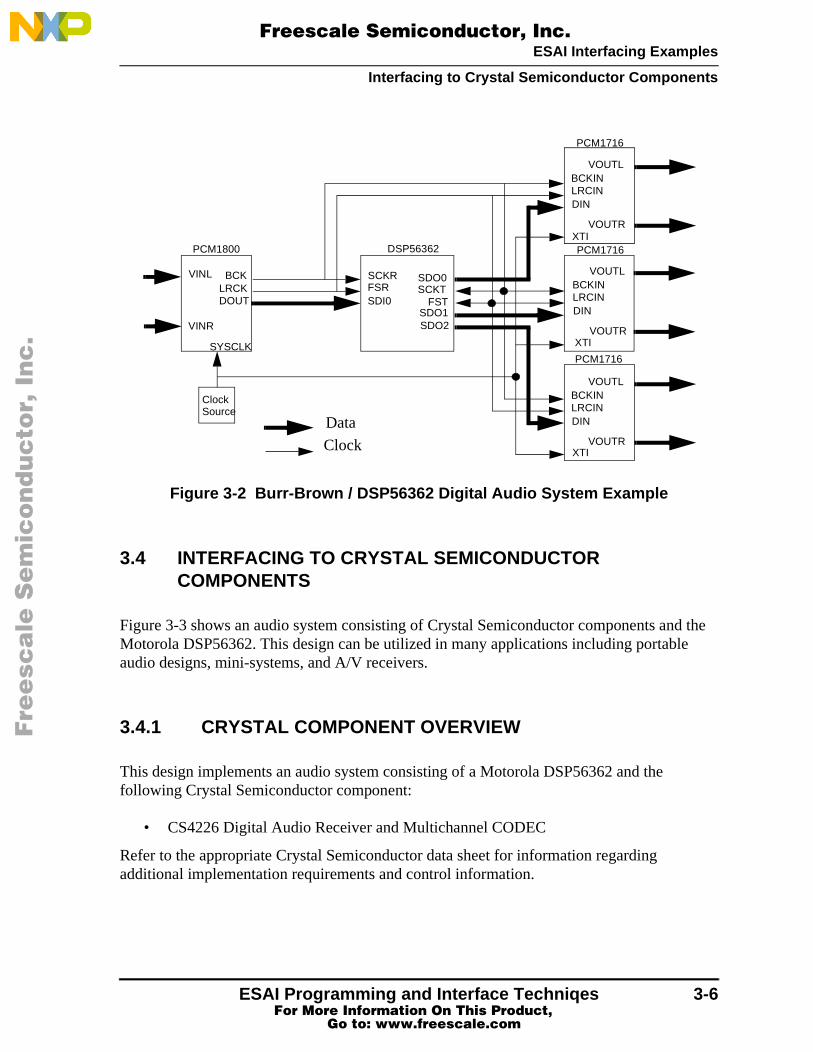
3.4 INTERFACING TO CRYSTAL SEMICONDUCTOR COMPONENTS
Figure 3-3 shows an audio system consisting of Crystal Semiconductor components and the Motorola DSP56362. This design can be utilized in many applications including portable audio designs, mini-systems, and A/V receivers.
3.4.1 CRYSTAL COMPONENT OVERVIEW
This design implements an audio system consisting of a Motorola DSP56362 and the following Crystal Semiconductor component:
• CS4226 Digital Audio Receiver and Multichannel CODEC
Refer to the appropriate Crystal Semiconductor data sheet for information regarding additional implementation requirements and control information.
ClockSource
DOUTLRCK
BCK
SYSCLK
FSRSCKR
SDI0 FSTSCKTSDO0
SDO1SDO2
BCKINLRCINDIN
VOUTL
VOUTR
BCKINLRCINDIN
VOUTL
VOUTR
BCKINLRCINDIN
VOUTL
VOUTR
VINL
VINR
PCM1800 DSP56362 PCM1716
PCM1716
PCM1716
Data
Clock XTI
XTI
XTI
ESAI Programming and Interface Techniqes 3-6 For More Information On This Product,
Go to: www.freescale.com
ESAI Interfacing Examples
Interfacing to Crystal Semiconductor Components
F
ree
sca
le S
em
ico
nd
uc
tor,
I
Freescale Semiconductor, Inc.n
c..
.
The CS4226 is a high performance single chip CODEC that provides a stereo 20-bit ADC and six channels of 20-bit DACs. Volume control for each of the six DAC channels is supported. A S/PDIF receiver is included as well as a mono 20-bit ADC in this single chip design.
3.4.2 SYSTEM OVERVIEW
This design provides a stereo analog input as well as a secondary mono input for applications such as karaoke. Three stereo analog inputs are sourced to the CS4226 with either the stereo or mono input being switched to the ADC at a time. Six channels of analog output are provided along with independently controlled volume controls and de-emphasis operation. The S/PDIF receiver can support one of four switchable inputs. This system supports sample rates of 32 kHz, 44.1 kHz, or 48 kHz.
In a mini-system or A/V receiver this system supports multiple digital audio input sources (i.e. DVD, VCR, Set top box, CD) and it supports multiple analog inputs (i.e. tuner, CD, VCR, etc...). The secondary mono analog input can be utilized for functions such as karaoke. As in the previous examples, the DSP can be used in this system to perform many digital audio functions including decoding Dolby Digital, DTS, and MPEG bitstreams, and Dolby Pro Logic processing. It can also support features such as equalization, tone/balance control, volume control, karaoke processes, or soundfield processing (i.e. Hall effects).
3.4.3 IMPLEMENTATION
3.4.3.1 Data InterfaceThe four digital audio inputs are provided using the CS4226 at inputs RX1, RX2, RX3, and RX4. The CS4226 selects one of the four inputs to send to the DSP using the SDOUT1 pin. Stereo analog inputs are available at the AINL1L/R, AINL2L/R, or AINL3L/R inputs. The CS4226 can send any of the following combinations of data to the DSP:
1. Stereo ADC to SDOUT1Mono ADC to SDOUT2
2. S/PDIF to SDOUT1Mono ADC to SDOUT2
3. S/PDIF to SDOUT1Stereo ADC to SDOUT2
SDOUT1 is received by the ESAI peripheral of the DSP at pin SDI0. SDOUT2 is received by the ESAI peripheral of the DSP at pin SDI1.
ESAI Programming and Interface Techniqes 3-7 For More Information On This Product,
Go to: www.freescale.com

ESAI Interfacing Examples
Interfacing to Crystal Semiconductor Components
F
ree
sca
le S
em
ico
nd
uc
tor,
I
Freescale Semiconductor, Inc.n
c..
.
The DSP processes the data provided from the CS4226 and outputs six channels of digital data using ESAI transmit pins (SDO0, SDO1 and SDO2) to the CS4226 digital input section (SDIN1, SDIN2, and SDIN3). The six channels of digital data is converted to analog signals by the CS4226 and output using pins AOUT1, AOUT2, AOUT3, AOUT4, AOUT5 and AOUT6.
The Crystal Semiconductor CS4226 operates using a 5.0 V power source while the DSP56362 is supported using 3.3 V power sources. The DSP563632 ESAI is 5.0 V tolerant and can support the levels required by the CS4226.
3.4.3.2 System ClockingSystem level clocks can be generated from the S/PDIF input which carries both clock and data information. When there are no S/PDIF signals, the CS4226 utilizes the external clock source at pin XTI to generate the system clocks. The CS4226 operates in master mode and provides the bitclock and framesync clock, while the DSP56362 ESAI is programmed to operate in slave mode.
Figure 3-3 Crystal Semiconductor/DSP56362 Digital Audio System
AOUT6AOUT5AOUT4AOUT3AOUT2AOUT1
SDIN2SDIN1
SDIN3
SCLKLRCKSDOUT1SDOUT2
AIN1LAIN1R
RX1
XTI
FSRSCKR
SDI0FSTSCKT
SDO0SDO1SDO2
DSP56362
SDI1
ClockSource
RX2RX3RX4
AINAUXDataClock
3-8 AI Programming and Interface Techniqes MOTOROLA For More Information On This Product,
Go to: www.freescale.com

Digital Audio Transfer Protocols
Introduction
ure
F
ree
sca
le S
em
ico
nd
uc
tor,
I
Freescale Semiconductor, Inc.n
c..
.
SECTION 4
DIGITAL AUDIO TRANSFER PROTOCOLS
4.1 INTRODUCTION
The receiver and transmitter sections can be programmed independently to support one of many different digital audio protocols. The clocking characteristics, data format, data framing, and number of slots utilized per sample (multiplexing) are programmed in the ESAI. The following sections provide an overview of the various digital audio data transfer characteristics and ESAI programmability, as well as the most common interface protocols implemented for audio applications.
4.2 PROGRAMMABLE I/O CHARACTERISTICS
Audio signals are usually transferred over a three line interface consisting of:
1. A bit clock
2. A framesync clock
3. Data
Figure 4-1 shows numerous methods for formatting the data in relation to the bit clock and framesync clock.
• Data can be shifted Most Significant Bit (MSB) first (see example A and B of Fig3-1) or Least Significant Bit (LSB) first (see example C and D of Figure 3-1).
• Data can be 8, 12, 16, 18, 20 or 24 bits in length.
• Data can be framed left justified with respect to the framesync’s transition (see example A and C of Figure 3-1), or right justified (see example B and D of Figure3-1).
There are also several ways to format each of the bit clocks and framesync clocks.
ESAI Programming and Interface Techniqes 4-1 For More Information On This Product,
Go to: www.freescale.com

Digital Audio Transfer Protocols
Programmable I/O Characteristics
e
(one high
le A
d of
F
ree
sca
le S
em
ico
nd
uc
tor,
I
Freescale Semiconductor, Inc.n
c..
.
• The bit clock can latch data on the rising edge or falling edge of the bit clock. SeFigure 4-2.
• The framesync can be word length (8, 12, 16, 20, 24, or 32 bits long) or bit lengthbit long as shown in example C in Figure 4-3) and can indicate frame start on thelevel portion or low level portion of the framesync clock.
• Framesync can also be aligned to occur together with the data word (see exampand B of Figure 4-3) or one bit earlier (see example C in Figure 4-3).
• For multiplexing applications, the ESAI framesync can indicate the first data wormany data words in a given frame.
Figure 4-1 Data Formatting
Framesync
Bit Clock
A) Data
(SCKR,SCKT)
(FSR,FST)
(SDIx,SDOx)
MSB LSB MSB LSB
B) Data(SDIx,SDOx)
MSB LSB MSB LSB
C) Data(SDIx,SDOx)
LSB MSB LSB MSB
D) Data(SDIx,SDOx)
LSB MSB LSB MSB
23 0
23 0 23 0
23 0
0 23
0 23 0 23
0 23
MSB First,
Left Justified
MSB First,
Right Justified
LSB First,
Left Justified
LSB First,
Right Justified
4-2 AI Programming and Interface Techniqes MOTOROLA For More Information On This Product,
Go to: www.freescale.com

Digital Audio Transfer Protocols
Programmable I/O Characteristics
F
ree
sca
le S
em
ico
nd
uc
tor,
I
Freescale Semiconductor, Inc.n
c..
.
Figure 4-2 Bit Clock Formatting
Figure 4-3 Framesync Formatting
Some combinations are more common than others and although the ESAI can be programmed to implement any one of the many possible clocking and data formats, this application note will focus on three of the most common interface protocols in digital audio. From these examples, users should be able to understand how to program this peripheral for any other desired configuration. The transfer protocols that are utilized in this application note are the I2S, left justified method, and EIAJ (right justified) format. Each of these protocols utilizes
Framesync
Bit Clock
Data
(SCKR,SCKT)
(FSR,FST)
(SDIx,SDOx)
A. Data Latched on Bit Clock’s falling edge
23 0
A) Framesync
Bit Clock
Data
(SCKR,SCKT)
(FSR,FST)
(SDIx,SDOx)
MSB LSB MSB LSB
B) Framesync (FSR,FST)
C) Framesync (FSR,FST)
23 0 23 0
Framesync Word Aligned
Frame Start High
Framesync Word Aligned
Frame Start Low
Framesync Bit Aligned
One Clock Early
(32 bit word length)
(32 bit word length)
(32 bit word length)
ESAI Programming and Interface Techniqes 4-3 For More Information On This Product,
Go to: www.freescale.com
Digital Audio Transfer Protocols
I2S, Left-Justified, and EIAJ (Right Justified) Formats
SB) erent th. If d, but
in
ly 32
dge dge of clock.
F
ree
sca
le S
em
ico
nd
uc
tor,
I
Freescale Semiconductor, Inc.n
c..
.
very different clocking, framing, and data formatting characteristics, so examples are provided that show how each characteristic is programmed to generate these protocols.
4.3 I2S, LEFT-JUSTIFIED, AND EIAJ (RIGHT JUSTIFIED) FORMATS
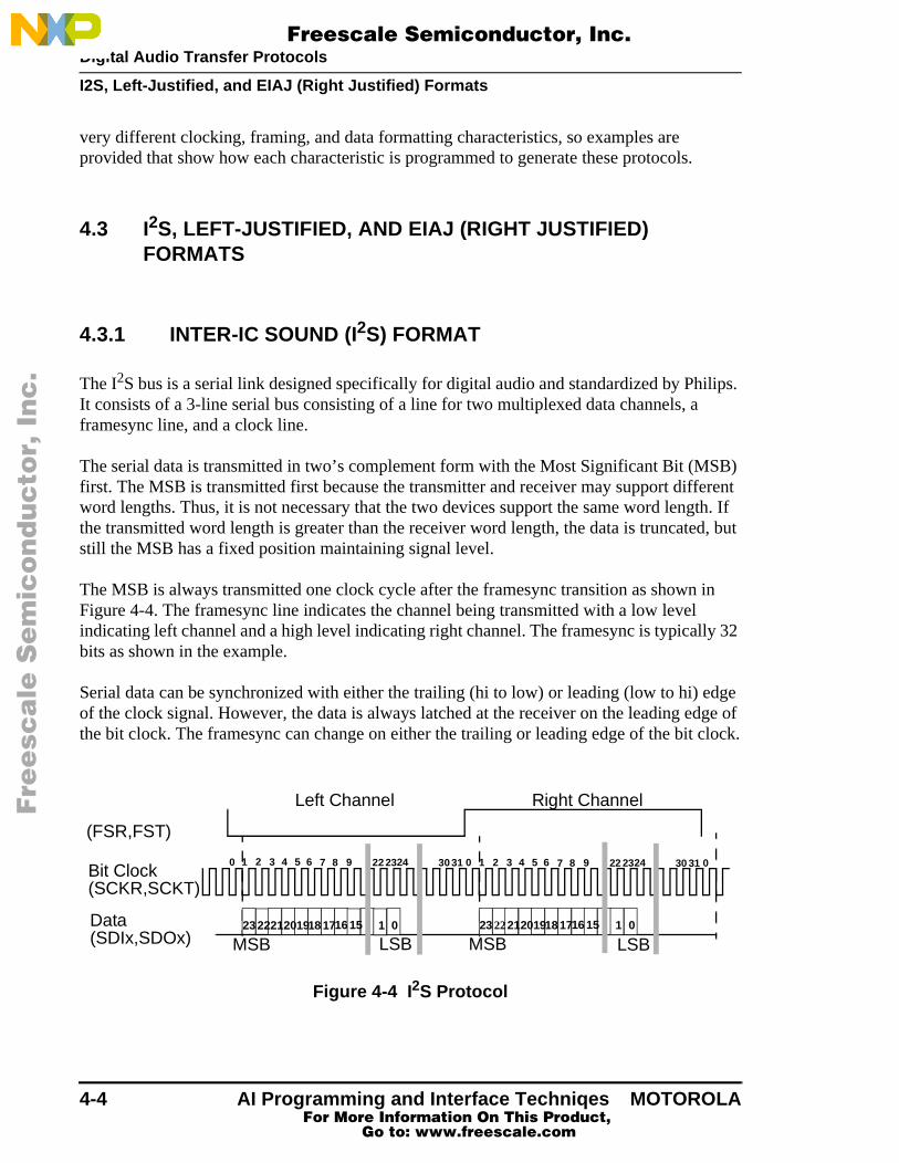
4.3.1 INTER-IC SOUND (I2S) FORMAT
The I2S bus is a serial link designed specifically for digital audio and standardized by Philips. It consists of a 3-line serial bus consisting of a line for two multiplexed data channels, a framesync line, and a clock line.
The serial data is transmitted in two’s complement form with the Most Significant Bit (Mfirst. The MSB is transmitted first because the transmitter and receiver may support diffword lengths. Thus, it is not necessary that the two devices support the same word lengthe transmitted word length is greater than the receiver word length, the data is truncatestill the MSB has a fixed position maintaining signal level.
The MSB is always transmitted one clock cycle after the framesync transition as shownFigure 4-4. The framesync line indicates the channel being transmitted with a low level indicating left channel and a high level indicating right channel. The framesync is typicalbits as shown in the example.
Serial data can be synchronized with either the trailing (hi to low) or leading (low to hi) eof the clock signal. However, the data is always latched at the receiver on the leading ethe bit clock. The framesync can change on either the trailing or leading edge of the bit
Figure 4-4 I2S Protocol
Bit Clock
Data
(SCKR,SCKT)
(FSR,FST)
(SDIx,SDOx) MSB LSB MSB LSB232221201918 171615 1 0 23 22212019181716 15 1 0
Left Channel Right Channel
0 1 2 3 4 5 6 7 8 9 22 2324 30 31 0 1 2 3 4 5 6 7 8 9 22 2324 30 31 0
4-4 AI Programming and Interface Techniqes MOTOROLA For More Information On This Product,
Go to: www.freescale.com
Digital Audio Transfer Protocols
I2S, Left-Justified, and EIAJ (Right Justified) Formats
F
ree
sca
le S
em
ico
nd
uc
tor,
I
Freescale Semiconductor, Inc.n
c..
.
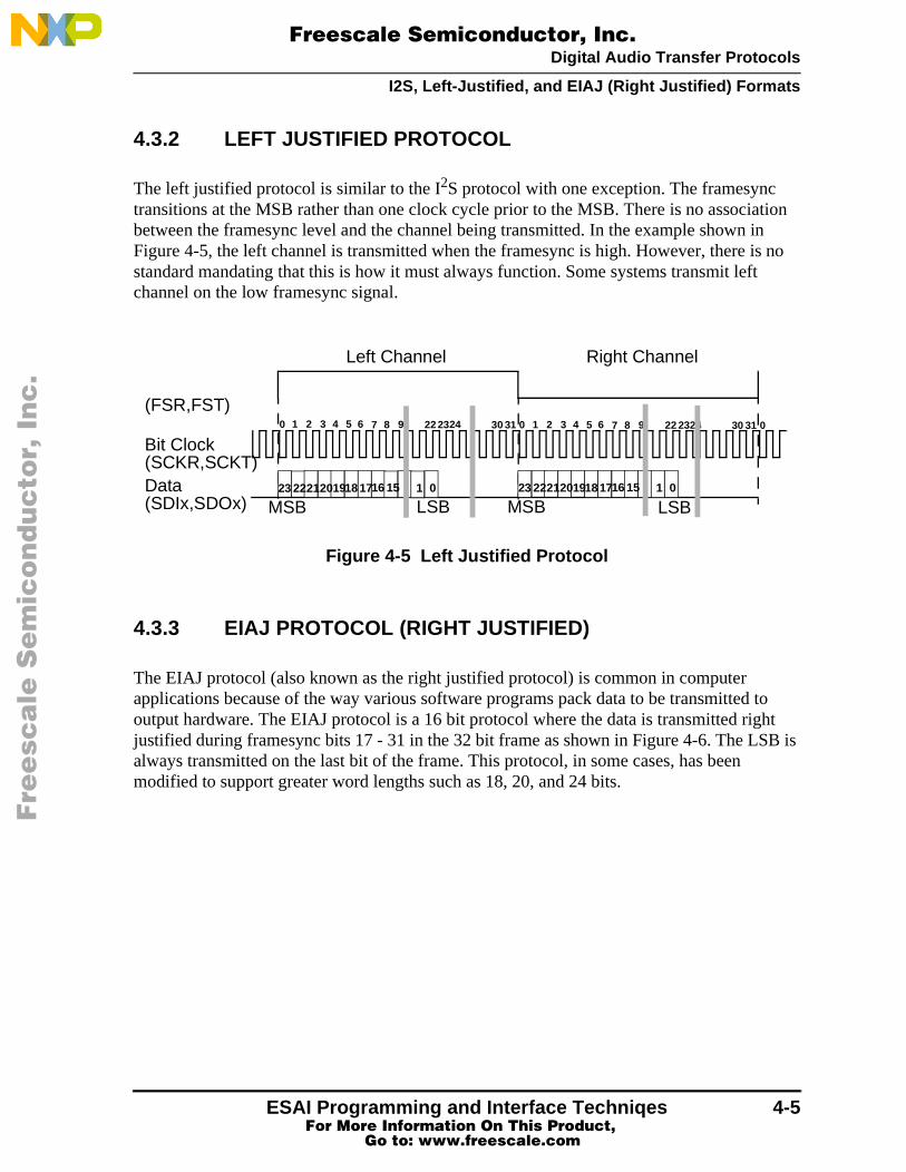
4.3.2 LEFT JUSTIFIED PROTOCOL
The left justified protocol is similar to the I2S protocol with one exception. The framesync transitions at the MSB rather than one clock cycle prior to the MSB. There is no association between the framesync level and the channel being transmitted. In the example shown in Figure 4-5, the left channel is transmitted when the framesync is high. However, there is no standard mandating that this is how it must always function. Some systems transmit left channel on the low framesync signal.
Figure 4-5 Left Justified Protocol
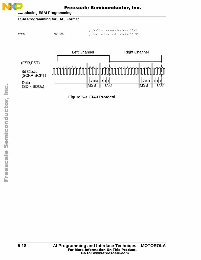
4.3.3 EIAJ PROTOCOL (RIGHT JUSTIFIED)
The EIAJ protocol (also known as the right justified protocol) is common in computer applications because of the way various software programs pack data to be transmitted to output hardware. The EIAJ protocol is a 16 bit protocol where the data is transmitted right justified during framesync bits 17 - 31 in the 32 bit frame as shown in Figure 4-6. The LSB is always transmitted on the last bit of the frame. This protocol, in some cases, has been modified to support greater word lengths such as 18, 20, and 24 bits.
Bit Clock
Data(SCKR,SCKT)
(FSR,FST)
(SDIx,SDOx) MSB LSB MSB LSB23 22212019181716 15 1 0 23 22212019181716 15 1 0
Left Channel Right Channel
0 1 2 3 4 5 6 7 8 9 22 2324 30 31 0 1 2 3 4 5 6 7 8 9 22 2324 30 31 0
ESAI Programming and Interface Techniqes 4-5 For More Information On This Product,
Go to: www.freescale.com

Digital Audio Transfer Protocols
I2S, Left-Justified, and EIAJ (Right Justified) Formats
F
ree
sca
le S
em
ico
nd
uc
tor,
I
Freescale Semiconductor, Inc.n
c..
.
Figure 4-6 EIAJ ProtocolThe following section overviews the ESAI programming registers and provides several examples for setting up the ESAI for I2S, left justified, and EIAJ protocols.
Bit Clock
Data
(SCKR,SCKT)
(FSR,FST)
(SDIx,SDOx) MSB LSB15 1413 1 0
Left Channel Right Channel
0 1 2 3 4 5 6 7 8 9 17 18 19 30 31 0 1 2 3 4 5 6 7 8 9 22 23 24 30 31 0
2
MSB LSB15 1413 1 0 2
ESAI Programming and Interface Techniqes 4-6 For More Information On This Product,
Go to: www.freescale.com

Introducing ESAI Programming
Introduction
sters
F
ree
sca
le S
em
ico
nd
uc
tor,
I
Freescale Semiconductor, Inc.n
c..
.
SECTION 5
INTRODUCING ESAI PROGRAMMING
5.1 INTRODUCTION
Several registers are provided for programming the operation of the ESAI. The ESAI provides generous flexibility by allowing users to have control over clocking and data formatting schemes for each of the transmitters and receivers. The following provides an overview of the ESAI programming registers and examples for implementation of the ESAI in I2S, Left Justified, and EIAJ formats. Refer to the DSP56362 User’s Manual for additional details on the programming registers.
5.2 ESAI PROGRAMMING OVERVIEW
ESAI programming is performed using several control registers described in the following sections. The functionality of the ESAI pins is controlled by the Port C Control register (PCRC) and the Port C Direction register (PRRC). These registers establish whether the ESAI pins are used for GPIO or as ESAI peripheral pins. The following registers are used when programmed as ESAI peripheral pins. One general purpose control register (SAICR) controls clocking characteristics common to both the receiver and transmitter. The ESAI receiver section is controlled with four control registers:
1. Two receive control registers — RCCR and RCR
2. Two receive slot mask registers — RSMA and RSMB
The transmitter section is controlled with four registers:
1. Two transmit control registers — TCCR and TCR
2. Two transmit slot mask registers — TSMA and TSMB
One status register (SAISR) is also provided for monitoring ESAI operation. These regiare covered in detail in the DSP56362 User’s Manual. This section provides an overview of their use in supporting conventional audio transfer protocols.
ESAI Programming and Interface Techniqes 5-1 For More Information On This Product,
Go to: www.freescale.com

Introducing ESAI Programming
General Purpose I/O (GPIO)
F
ree
sca
le S
em
ico
nd
uc
tor,
I
Freescale Semiconductor, Inc.n
c..
.
5.3 GENERAL PURPOSE I/O (GPIO)
The ESAI pins can be utilized as general purpose input/output (GPIO) pins when not used for ESAI functionality. In some applications, not all ESAI pins are necessary for data transfer and can be programmed to operate as GPIO pins. The ESAI/GPIO pin relationship is shown in Table 5-1. Two registers determine the functionality of the ESAI pins:
1. Port C Control register (PCRC)
2. Port C Direction register (PRRC)
The read/write PCRC register is shown in Table 5-2. The PCRC register operates in conjunction with the read/write PRRC register shown in Table 5-3. The PRRC register controls the functionality of the ESAI pins as shown in Table 5-4.
Operation of the ESAI pins in GPIO mode is not covered in this application note. The following example code programs the ESAI for operation with two ESAI inputs, three ESAI outputs and three GPIO pins:
movep #$000edb,x:M_PCRC ;Enable all ESAI pins except HCKR, HCKT, and SDO3movep #$000edb,x:M_PRRC ;These operate as GPIO pins PC2, PC5, and PC8
Table 5-1 ESAI/GPIO Pin Designation
ESAI Pin GPIO Pin
SCKR PC0
FSR PC1
HCKR PC2
SCKT PC3
FST PC4
HCKT PC5
SDO5/SDI0 PC6
SDO4/SDI1 PC7
SDO3/SDI2 PC8
SDO2/SDI3 PC9
SDO1 PC10
SDO0 PC11
ESAI Programming and Interface Techniqes 5-2 For More Information On This Product,
Go to: www.freescale.com

Introducing ESAI Programming
General Purpose I/O (GPIO)
F
ree
sca
le S
em
ico
nd
uc
tor,
I
Freescale Semiconductor, Inc.n
c..
.
Table 5-2 Port C Control Register (PCRC)
BITS 11 10 9 8 7 6 5 4 3 2 1 0
FIELD PC11 PC10 PC9 PC8 PC7 PC6 PC5 PC4 PC3 PC2 PC1 PC0
R/W R/W
BITS 23 22 21 20 19 18 17 16 15 14 13 12
FIELD Reserved (Read and Write with 0)
R/W R/W
Table 5-3 Port C Data Register (PRRC)
BITS 11 10 9 8 7 6 5 4 3 2 1 0
FIELD PD11 PD10 PD9 PD8 PD7 PD6 PD5 PD4 PD3 PD2 PD1 PD0
R/W R/W
BITS 23 22 21 20 19 18 17 16 15 14 13 12
FIELD Reserved (Read and Write with 0)
R/W R/W
Table 5-4 PCRC and PRRC Bit Functionality
PDC[i] PC[i] Port Pin[i] Function
0 0 Disconnected
0 1 GPIO input
1 0 GPIO output
1 1 ESAI
ESAI Programming and Interface Techniqes 5-3 For More Information On This Product,
Go to: www.freescale.com

Introducing ESAI Programming
General Purpose I/O (GPIO)
F
ree
sca
le S
em
ico
nd
uc
tor,
I
Freescale Semiconductor, Inc.n
c..
.
5.3.1 ESAI CONTROL AND STATUS REGISTERS
5.3.1.1 ESAI Control Register (SAICR)SAICR enables/disables synchronous clock capabilities (where the transmitter clocks can be operated synchronously with the receiver clocks) and control for alignment of data to bit 15 (when bit length is 16, 12 or 8) rather than bit 23. See Table 5-5. This register is commonly cleared in conventional digital audio applications indicating asynchronous operation where the receiver and transmitter sections operate from independent external clock sources.
Table 5-5 ESAI Common Control Register (SAICR)
BITS 11 10 9 8 7 6 5 4 3 2 1 0
FIELD Reserved ALC TEBE SYN Reserved OF2 OF1 OF0
R/W R/W
BITS 23 22 21 20 19 18 17 16 15 14 13 12
FIELD Reserved (Read and Write with 0)
R/W R/W
ADDR X:$FFFFB4
Table 5-6 SAICR Field Descriptions
Bits Name Description
0, 1, 2 OF Output Flags - not applicable
6 SYN Synchronous/Asynchronous Operation
7 TEBE FSR control
8 ALC Data bit alignment for bits 16/23
ESAI Programming and Interface Techniqes 5-4 For More Information On This Product,
Go to: www.freescale.com

Introducing ESAI Programming
General Purpose I/O (GPIO)
F
ree
sca
le S
em
ico
nd
uc
tor,
I
Freescale Semiconductor, Inc.n
c..
.
5.3.1.2 ESAI Status Register (SAISR)SAISR provides status of the receiver and transmitter data registers. The SAISR is shown in Table 5-7. User programs can monitor this register as a method of polling the receiver and transmitter.
Table 5-7 ESAI Status Register (SAISR)
BITS 11 10 9 8 7 6 5 4 3 2 1 0
FIELD Rsvd RODF REDF RDF ROE RFS Reserved IF2 IF1 IF0
R/W R/W
BITS 23 22 21 20 19 18 17 16 15 14 13 12
FIELD Reserved (Read and Write with 0) TODE TEDE TDE TUE TFS Rsvd
R/W R/W
ADDR X:$FFFFB3
Table 5-8 SAISR Field Descriptions
Bits Name Description
0 IFO Bit clock input flag
1 IF1 Framesync clock input flag
2 IF2 High Frequency clock input Flag
3,4,5 Reserved
Receiver Flags
6 RFS Framesync Flag
7 ROE Overrun error Flag
8 RDF Data full Flag
9 REDF Even Data full Flag
10 RODF Odd Data full Flag
Transmitter Flags
11,12 Reserved
13 TFS Framesync Flag
14 TUE Underrun error Flag
15 TDE Data empty Flag
16 TEDE Even Data empty Flag
17 TODE Odd Data empty Flag
ESAI Programming and Interface Techniqes 5-5 For More Information On This Product,
Go to: www.freescale.com

Introducing ESAI Programming
General Purpose I/O (GPIO)
F
ree
sca
le S
em
ico
nd
uc
tor,
I
Freescale Semiconductor, Inc.n
c..
.
5.3.2 ESAI RECEIVER CONTROL REGISTERS
There are two receiver control registers:
1. Receive clock control register (RCCR)
2. Receive control register (RCR)
5.3.2.1 RCCR RegisterThe RCCR controls clocking of the receiver section of the ESAI. The read/write RCCR controls the ESAI receiver clock. Various characteristics of the receiver clock can be controlled by the RCCR as shown in Table 5-9 and described in Table 5-10.
Table 5-9 ESAI Receive Clock Control Register (RCCR)
BITS 11 10 9 8 7 6 5 4 3 2 1 0
FIELD RDC2 RDC1 RDC0 RPSR RPM7 RPM6 RPM5 RPM4 RPM3 RPM2 RPM1 RPM0
R/W R/W
BITS 23 22 21 20 19 18 17 16 15 14 13 12
FIELD RHCKD RFSD RCKD RHCKP RFSP RCKP RFP3 RFP2 RFP1 RFP0 RDC4 RDC3
R/W R/W
ADDR X:$FFFFB8
Table 5-10 RCCR Field Descriptions
Bits Name Description
0 - 7 RPM Prescaler Ratio
8 RPSR Divide by Prescaler
9-13 RDC Frame Rate Divider
14-17 RFP High Frequency clock divider
18 RCKP Bit clock polarity
19 RFSP Framesync clock polarity
20 RHCKP High frequency clock polarity
21 RCKD Bit clock source (internal/external)
22 RFSD Framesync clock source (internal/external)
23 RHCKD High Frequency clock source (internal/external)
ESAI Programming and Interface Techniqes 5-6 For More Information On This Product,
Go to: www.freescale.com

Introducing ESAI Programming
General Purpose I/O (GPIO)
F
ree
sca
le S
em
ico
nd
uc
tor,
I
Freescale Semiconductor, Inc.n
c..
.
5.3.2.2 RCCR Example Codemovep #$080200,x:M_RCCR ;FSR is input(bit22=0) ;external clock source drives SCKR
;(bit21=0) ;negative FSR polarity(bit19=1) ;data & FSR clocked in on rising edge
;(bit18=0) ;2 words per frame (bit13:9=00001)
5.3.2.3 RCR RegisterThe read/write RCR controls the ESAI receiver section. Various ESAI receiver pins can be enabled/disabled and characteristics of the receive transfer protocol can be controlled by the RCR as shown in Table 5-11 and described in Table 5-12.
Table 5-11 ESAI Receive Control Register (RCR)
BITS 11 10 9 8 7 6 5 4 3 2 1 0
FIELD RSWS1 RSWS0 RMOD1 RMOD0 RWA RSHFD Reserved (R/W as 0) RE3 RE2 RE1 RE0
R/W R/W
BITS 23 22 21 20 19 18 17 16 15 14 13 12
FIELDRLIE RIE REDIE REIE RPR Reserved (R/W as
0)RFSR RFSL RSWS4 RSWS3 RSWS2
R/W R/W
ADDR X:$FFFFB7
Table 5-12 RCR Field Descriptions
Bits Name Description
0 - 3 RE Inputs enabled
4-5 Reserved
6 RSHFD Data shift direction MSB first/LSB first
7 RWA Word alignment left justified/right justified
8-9 MODx Operating mode
10-14 RSWS Word length and slot length
15 RFSL Framesync length
16 RFSR Framesync timing
19 RPR Receiver Personal Reset
ESAI Programming and Interface Techniqes 5-7 For More Information On This Product,
Go to: www.freescale.com

Introducing ESAI Programming
General Purpose I/O (GPIO)
F
ree
sca
le S
em
ico
nd
uc
tor,
I
Freescale Semiconductor, Inc.n
c..
.
5.3.2.4 RCR Example Code movep #$d17D02,x:M_RCR;RX1 enabled (bit1=1)
;RX0,RX2,RX3 disabled (bit3:2,0=000);reserved (bit5:4=00);MSB shifted first (bit6=0);word left-aligned (bit7=0);network mode (bit9:8=01);32-bit slot length,;24-bit word length (bit14:10=11111)
;word-length frame sync (bit15=0);frame sync occurs 1 clock cycle earlier (bit16=1)
;reserved (bit19:17=000);RLIE, RIE, REIE enabled
; (bit23:20=1101)
5.3.2.5 RSMA and RSMB registersRSMA and RSMB are two read/write registers used by the receivers when programmed in network mode to determine for each slot (up to 32 slots) whether to receive a data word or to ignore the received data. Only the first 16 bits (15 - 0) are active for each of the RSMA and RSMB registers. RSMA and RSMB each control the enabling/disabling of 16 receive slots. RSMA controls the first 16 slots (slots 15 - 0) while RSMB controls the last 16 slots (slots 31 - 16). Each bit is used to enable/disable one of the 32 receiver slots. For example, if only the first two slots are to be used (left channel, right channel) bits 0 and 1 are set in RSMA, while the other 14 bits in RSMA, as well as all 16 bits of RSMB are cleared. For example, RSMA - $000003, RSMB - $000000.
20-23 REIE REDIE
RIE RLIE
Interrupts enable/disable
Table 5-12 RCR Field Descriptions (Continued)
Bits Name Description
ESAI Programming and Interface Techniqes 5-8 For More Information On This Product,
Go to: www.freescale.com
Introducing ESAI Programming
General Purpose I/O (GPIO)
F
ree
sca
le S
em
ico
nd
uc
tor,
I
Freescale Semiconductor, Inc.n
c..
.
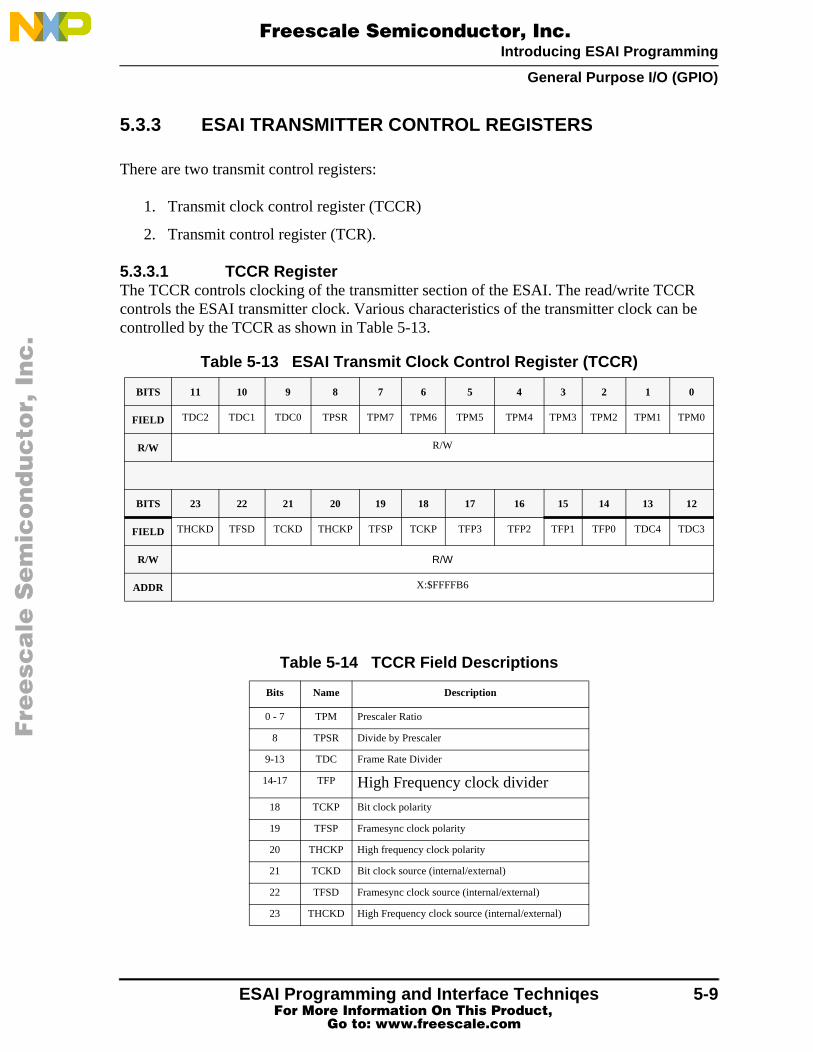
5.3.3 ESAI TRANSMITTER CONTROL REGISTERS
There are two transmit control registers:
1. Transmit clock control register (TCCR)
2. Transmit control register (TCR).
5.3.3.1 TCCR RegisterThe TCCR controls clocking of the transmitter section of the ESAI. The read/write TCCR controls the ESAI transmitter clock. Various characteristics of the transmitter clock can be controlled by the TCCR as shown in Table 5-13.
Table 5-13 ESAI Transmit Clock Control Register (TCCR)
BITS 11 10 9 8 7 6 5 4 3 2 1 0
FIELD TDC2 TDC1 TDC0 TPSR TPM7 TPM6 TPM5 TPM4 TPM3 TPM2 TPM1 TPM0
R/W R/W
BITS 23 22 21 20 19 18 17 16 15 14 13 12
FIELD THCKD TFSD TCKD THCKP TFSP TCKP TFP3 TFP2 TFP1 TFP0 TDC4 TDC3
R/W R/W
ADDR X:$FFFFB6
Table 5-14 TCCR Field Descriptions
Bits Name Description
0 - 7 TPM Prescaler Ratio
8 TPSR Divide by Prescaler
9-13 TDC Frame Rate Divider
14-17 TFP High Frequency clock divider
18 TCKP Bit clock polarity
19 TFSP Framesync clock polarity
20 THCKP High frequency clock polarity
21 TCKD Bit clock source (internal/external)
22 TFSD Framesync clock source (internal/external)
23 THCKD High Frequency clock source (internal/external)
ESAI Programming and Interface Techniqes 5-9 For More Information On This Product,
Go to: www.freescale.com

Introducing ESAI Programming
General Purpose I/O (GPIO)
F
ree
sca
le S
em
ico
nd
uc
tor,
I
Freescale Semiconductor, Inc.n
c..
.
5.3.3.2 TCCR Example Code movep #$0c0200,x:M_TCCR ;FST is input (bit22=0)
;external clock source drives SCKT (bit21=0);negative FST polarity (bit19=1);data & FST clocked out on rising edge (bit18=1);2 words per frame (bit13:9=00001)
5.3.3.3 TCR RegisterThe read/write TCR register controls the ESAI transmitter section. Various ESAI transmitter pins can be enabled/disabled and characteristics of the transmitter transfer protocol can be controlled by the TCR as shown in Table 5-15 and described in Table 5-16.
Table 5-15 ESAI Transmit Control Register (TCR)
BITS 11 10 9 8 7 6 5 4 3 2 1 0
FIELD TSWS1 TSWS0 TMOD1 TMOD0 TWA TSHFD TE5 TE4 TE3 TE2 TE1 TE0
R/W R/W
BITS 23 22 21 20 19 18 17 16 15 14 13 12
FIELDTLIE TIE TEDIE TEIE TPR RSVD
(R/W with o)PADC TFSR TFSL TSWS4 TSWS3 TSWS2
R/W R/W
ADDR X:$FFFFB5
Table 5-16 TCR Field Descriptions
Bits Name Description
0-5 TE Outputs enabled
6 TSHFD Data shift direction MSB first/LSB first
7 TWA Word alignment left justified/right justified
8-9 TMODx Operating mode
10-14 TSWS Word length and slot length
15 TFSL Framesync length
16 TFSR Framesync timing
17 PADC Zero Padding Control
ESAI Programming and Interface Techniqes 5-10 For More Information On This Product,
Go to: www.freescale.com

Introducing ESAI Programming
General Purpose I/O (GPIO)
F
ree
sca
le S
em
ico
nd
uc
tor,
I
Freescale Semiconductor, Inc.n
c..
.
5.3.3.4 TCR Example Code movep #$d13d00,x:M_TCR;TX0, TX1, TX2 enabled (bit3:0=0011)
;TX3, TX4, TX5 disabled (bit5:4=00);MSB shifted first (bit6=0);word left-aligned (bit7=0);network mode (bit9:8=01);32-bit slot length, 24-bit word length; (bit14:10=11111);word length frame sync (bit15=0);frame sync occurs 1 clock cycle earlier; (bit16=0);reserved (bit19:17=000);TLIE, TIE, TEIE enabled (bit23:20=0101)
5.3.3.5 TSMA and TSMB RegistersTSMA and TSMB are two read/write registers used by the transmitters in network mode to determine for each slot (up to 32 slots) whether to transmit a data word or to tri-state the transmitter pins. Only the first 16 bits (15 - 0) are active for each of the TSMA and TSMB registers. TSMA and TSMB each control the enabling/disabling of 16 transmit slots. TSMA controls the first 16 slots (slots 31-16) while TSMB control the last 16 slots (slots 15-0). Each bit is used to enable/disable one of the 32 transmitter slots. For example, if only the first two slots are to be used (left channel, right channel) bits 0 and 1 are set in TSMA while the other 14 bits in TSMA as well as all 16 bits in TSMB are cleared. i.e.e TSMA - $000003, TSMB - $000000.
19 TPR Transmitter Personal Reset
20-23 TEIE TEDIE
TIE TLIE
Interrupts enable/disable
Table 5-16 TCR Field Descriptions (Continued)
Bits Name Description
ESAI Programming and Interface Techniqes 5-11 For More Information On This Product,
Go to: www.freescale.com

Introducing ESAI Programming
ESAI Programing for I2S Format
F
ree
sca
le S
em
ico
nd
uc
tor,
I
Freescale Semiconductor, Inc.n
c..
.
5.4 ESAI PROGRAMING FOR I2S FORMAT
The following programs the ESAI for operation in slave mode using the I2S transfer protocol as shown in Figure 5-1. ESAI programing is as follows:
RCCR $0c0200 ;FSR is input;(bit22=0)
;external clock source drives SCKR;(bit21=0)
;negative FSR polarity ;(bit19=1)
;data & FSR clocked in on rising edge ;(bit18=0)
;2 words per frame ;(bit13:9=00001)
RCR $d17d02 ;RX1 enabled ;(bit1=1)
;RX0, RX2, RX3 disabled ;(bit3:2,0=000)
;reserved ;(bit5:4=00)
;MSB shifted first ;(bit6=0)
;word left-aligned ;(bit7=0)
;network mode ;(bit9:8=01)
;32-bit slot length, 24-bit word length ;(bit14:10=11111)
;word-length frame sync;(bit15=0)
;frame sync occurs 1 clock cycle earlier ;(bit16=1)
;reserved ;(bit19:17=000)
;RLIE, RIE, REIE enabled ;(bit23:20=0101)
RSMA $000003 ;enable receive slots 0 and 1;disable receive slots 15-2
RSMB $000000 ;disable receive slots 16-31
SAICR $000000 ;Flags 0, 1, and 2 not applicable ;(asynchronous mode);(bit2:0=0);asynchronous mode ;(bit 6=0);TEBE bit not applicable (asynchronous mode) ;(bit 7=0)
ESAI Programming and Interface Techniqes 5-12 For More Information On This Product,
Go to: www.freescale.com
Introducing ESAI Programming
ESAI Programing for I2S Format
F
ree
sca
le S
em
ico
nd
uc
tor,
I
Freescale Semiconductor, Inc.n
c..
.
;ALC bit cleared - 24 bit support;(bit 8=0)
TCCR $0c0200 ;FST is input;(bit22=0);external clock source drives SCKT;(bit21=0);negative FST polarity;(bit19=1);data & FST clocked out on rising edge ;(bit18=1);2 words per frame ;(bit13:9=00001)
TCR $d17d02 ;TX0, TX1, TX2 enabled;(bit3:0=0011)
;TX3, TX4, TX5 disabled ;(bit5:4=00)
;MSB shifted first;(bit6=0)
;word left-aligned;(bit7=0)
;network mode;(bit9:8=01)
;32-bit slot length, 24-bit word length ;(bit14:10=11111)
;word length frame sync;(bit15=0)
;frame sync occurs 1 clock cycle earlier ;(bit16=0)
;reserved ;(bit19:17=000)
;TLIE, TIE, TEIE enabled ;(bit23:20=0101)
TSMA $000003 ;enable transmit slot 0 and 1;disable transmitslots 15-2
TSMB $000003 ;disable transmit slots 16-31
Figure 5-1 I2S Protocol
Bit Clock
Data
(SCKR,SCKT)
(FSR,FST)
(SDIx,SDOx) MSB LSB MSB LSB23 22 21 201918 1716 15 1 0 23 22 21 201918 1716 15 1 0
Left Channel Right Channel
0 1 2 3 4 5 6 7 8 9 22 23 24 30 31 0 1 2 3 4 5 6 7 8 9 22 23 24 30 31 0
ESAI Programming and Interface Techniqes 5-13 For More Information On This Product,
Go to: www.freescale.com

Introducing ESAI Programming
ESAI Programming for Left Justified Format
F
ree
sca
le S
em
ico
nd
uc
tor,
I
Freescale Semiconductor, Inc.n
c..
.
5.5 ESAI PROGRAMMING FOR LEFT JUSTIFIED FORMAT
The following programs the ESAI for operation in slave mode using the Left Justified transfer protocol as shown in Figure 5-2. ESAI programing is as follows:
RCCR $080200 ;FSR is input;(bit22=0)
;external clock source drives SCKR;(bit21=0)
;positive FSR polarity;(bit19=0)
;data & FSR clocked in on rising edge ;(bit18=0)
;2 words per frame ;(bit13:9=00001)
RCR $d07d02 ;RX1 enabled;(bit1=1)
;RX0, RX2, RX3 disabled ;(bit3:2,0=000)
;reserved;(bit5:4=00)
;MSB shifted first;(bit6=0)
;word left-aligned;(bit7=0)
;network mode;(bit9:8=01)
;32-bit slot length, 24-bit word length ;(bit14:10=11111)
;word-length frame sync;(bit15=0)
;frame sync occurs at MSB;(bit16=0)
;reserved ;(bit19:17=000)
;RLIE, RIE, REIE enabled ;(bit23:20=1101)
RSMA $000003 ;enable receive slots 0 and 1;disable receive slots 15-2
RSMB $000000 ;disable receive slots 16-31
SAICR $000000 ;Flags 0, 1, and 2 not applicable ;(asynchronous mode)(bit2:0);asynchronous mode ;(bit 6);TEBE bit not applicable (asynchronous mode) ;(bit 7);ALC bit cleared - 24 bit support
ESAI Programming and Interface Techniqes 5-14 For More Information On This Product,
Go to: www.freescale.com

Introducing ESAI Programming
ESAI Programming for Left Justified Format
F
ree
sca
le S
em
ico
nd
uc
tor,
I
Freescale Semiconductor, Inc.n
c..
.
;(bit 8)
TCCR $080200 ;FST is input;(bit22=0);external clock source drives SCKT;(bit21=0);positive FST polarity;(bit19=0);data & FST clocked out on rising edge ;(bit18=1);2 words per frame ;(bit13:9=00001)
TCR $d07d02 ;TX0, TX1, TX2 enabled;(bit3:0=0011)
;TX3, TX4, TX5 disabled;(bit5:4=00)
;MSB shifted first;(bit6=0)
;word left-aligned;(bit7=0)
;network mode;(bit9:8=01)
;32-bit slot length, 24-bit word length ;(bit14:10=11111)
;word length frame sync;(bit15=0)
;frame sync occurs at MSB;(bit16=0)
;reserved ;(bit19:17=000)
;TLIE, TIE, TEIE enabled ;(bit23:20=1101)
TSMA $000003 ;enable transmit slot 0 and 1;disable transmitslots 15-2
TSMB $000003 ;disable transmit slots 16-31
ESAI Programming and Interface Techniqes 5-15 For More Information On This Product,
Go to: www.freescale.com

Introducing ESAI Programming
ESAI Programming for EIAJ Format
F
ree
sca
le S
em
ico
nd
uc
tor,
I
Freescale Semiconductor, Inc.n
c..
.
Figure 5-2 Left Justified Protocol5.6 ESAI PROGRAMMING FOR EIAJ FORMAT
The following programs the ESAI for operation in slave mode using the EIAJ transfer protocol as show in Figure 5-3. ESAI programing is as follows:
RCCR $0c0200 ;FSR is input;(bit22=0)
;external clock source drives SCKR;(bit21=0)
;negative FSR polarity;(bit19=1)
;data & FSR clocked in on rising edge ;(bit18=0)
;2 words per frame ;(bit13:9=00001)
RCR $d04982 ;RX1 enabled;(bit1=1)
;RX0, RX2, RX3 disabled ;(bit3:2,0=000)
;reserved;(bit5:4=00)
;MSB shifted first;(bit6=0)
;word right-aligned;(bit7=1)
;network mode;(bit9:8=01)
;32-bit slot length, 16-bit word length ;(bit14:10=10010)
;word-length frame sync;(bit15=0)
;frame sync occurs following LSB;(bit16=0)
Bit Clock
Data
(SCKR,SCKT)
(FSR,FST)
(SDIx,SDOx) MSB LSB MSB LSB23 22 21 201918 1716 15 1 0 23 22 21 201918 1716 15 1 0
Left Channel Right Channel
0 1 2 3 4 5 6 7 8 9 22 23 24 30 31 0 1 2 3 4 5 6 7 8 9 22 23 24 30 31 0
ESAI Programming and Interface Techniqes 5-16 For More Information On This Product,
Go to: www.freescale.com

Introducing ESAI Programming
ESAI Programming for EIAJ Format
F
ree
sca
le S
em
ico
nd
uc
tor,
I
Freescale Semiconductor, Inc.n
c..
.
;reserved ;(bit19:17=000)
;RLIE, RIE, REIE enabled ;(bit23:20=1101)
RSMA $000003 ;enable receive slots 0 and 1;disable receive slots 15-2
RSMB $000000 ;disable receive slots 16-31
SAICR $000100 ;Flags 0,1,and 2 N/A (asynchronous mode);(bit2:0=0);asynchronous mode;(bit 6=0);TEBE bit not applicable (asynchronous mode) ;(bit7=0);ALC bit cleared - 16 bit support aligned to ;bit 15
; ;(bit 8=1)
TCCR $0c0200 ;FST is input;(bit22=0);external clock source drives SCKT;(bit21=0);negative FST polarity;(bit19=1);data & FST clocked out on rising edge ;(bit18=1);2 words per frame ;(bit13:9=00001)
TCR $d04982 ;TX0, TX1, TX2 enabled;(bit3:0=0011)
;TX3, TX4, TX5 disabled;(bit5:4=00)
;MSB shifted first;(bit6=0)
;word right-aligned;(bit7=1)
;network mode;(bit9:8=01)
;32-bit slot length, 16-bit word length ;(bit14:10=10010)
;word length frame sync;(bit15=0)
;frame sync occurs following LSB;(bit16=0)
;reserved ;(bit19:17=000)
;TLIE, TIE, TEIE enabled ;(bit23:20=1101)
TSMA $000003 ;enable transmit slot 0 and 1
ESAI Programming and Interface Techniqes 5-17 For More Information On This Product,
Go to: www.freescale.com
Introducing ESAI Programming
ESAI Programming for EIAJ Format
F
ree
sca
le S
em
ico
nd
uc
tor,
I
Freescale Semiconductor, Inc.n
c..
.
;disable transmitslots 15-2TSMB $000003 ;disable transmit slots 16-31
Figure 5-3 EIAJ Protocol
Bit Clock
Data
(SCKR,SCKT)
(FSR,FST)
(SDIx,SDOx) MSB LSB15 1413 1 0
Left Channel Right Channel
0 1 2 3 4 5 6 7 8 9 17 18 19 30 31 0 1 2 3 4 5 6 7 8 9 22 23 24 30 31 0
2
MSB LSB15 1413 1 0 2
5-18 AI Programming and Interface Techniqes MOTOROLA For More Information On This Product,
Go to: www.freescale.com
ESAI Programming Examples
Software Examples
ntation
-2.
is is re
AI
F
ree
sca
le S
em
ico
nd
uc
tor,
I
Freescale Semiconductor, Inc.n
c..
.
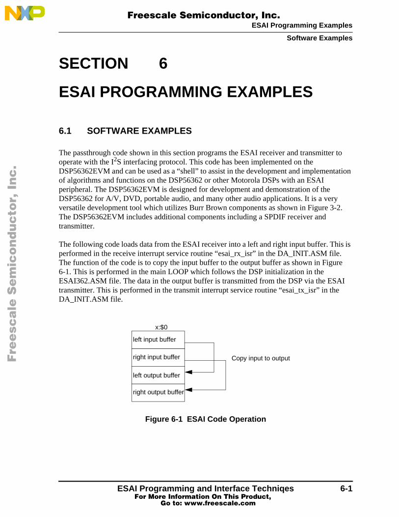
SECTION 6
ESAI PROGRAMMING EXAMPLES
6.1 SOFTWARE EXAMPLES
The passthrough code shown in this section programs the ESAI receiver and transmitter to operate with the I2S interfacing protocol. This code has been implemented on the DSP56362EVM and can be used as a “shell” to assist in the development and implemeof algorithms and functions on the DSP56362 or other Motorola DSPs with an ESAI peripheral. The DSP56362EVM is designed for development and demonstration of the DSP56362 for A/V, DVD, portable audio, and many other audio applications. It is a veryversatile development tool which utilizes Burr Brown components as shown in Figure 3The DSP56362EVM includes additional components including a SPDIF receiver and transmitter.
The following code loads data from the ESAI receiver into a left and right input buffer. Thperformed in the receive interrupt service routine “esai_rx_isr” in the DA_INIT.ASM file.The function of the code is to copy the input buffer to the output buffer as shown in Figu6-1. This is performed in the main LOOP which follows the DSP initialization in the ESAI362.ASM file. The data in the output buffer is transmitted from the DSP via the EStransmitter. This is performed in the transmit interrupt service routine “esai_tx_isr” in theDA_INIT.ASM file.
Figure 6-1 ESAI Code Operation
left input buffer
right input buffer
right output buffer
left output buffer
Copy input to output
x:$0
ESAI Programming and Interface Techniqes 6-1 For More Information On This Product,
Go to: www.freescale.com
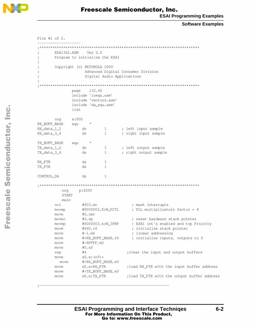
ESAI Programming Examples
Software Examples
F
ree
sca
le S
em
ico
nd
uc
tor,
I
Freescale Semiconductor, Inc.n
c..
.
File #1 of 2.--------------------;**************************************************************************; ESAI362.ASM Ver 2.0; Program to initialize the ESAI;; Copyright (c) MOTOROLA 2000; Advanced Digital Consumer Division ; Digital Audio Applications; ;************************************************************************** page 132,60 include ’ioequ.asm’ include ’vectors.asm’ include ’da_equ.asm’ list
org x:$00RX_BUFF_BASE equ *RX_data_1_2 ds 1 ; left input sampleRX_data_3_4 ds 1 ; right input sample
TX_BUFF_BASE equ *TX_data_1_2 ds 1 ; left output sampleTX_data_3_4 ds 1 ; right output sample
RX_PTR ds 1TX_PTR ds 1
CONTROL_DA ds 1
;************************************************************************** org p:$200 START main
ori #$03,mr ; mask interrupts movep #$050003,X:M_PCTL ; PLL multiplicatoin factor = 4 move #0,omr movec #0,sp ; reset hardware stack pointer movep #$000003,x:M_IPRP ; ESAI int’s enabled and top Priority move #$40,r6 ; initialize stack pointer move #-1,m6 ; linear addressing move #>RX_BUFF_BASE,r0 ; initialize inputs, outputs to 0 move #>$FFFF,m0 move #0,x0 rep #4 ;clear the input and output buffers move x0,x:(r0)+
move #>RX_BUFF_BASE,x0 move x0,x:RX_PTR ;load RX_PTR with the input buffer address move #>TX_BUFF_BASE,x0 move x0,x:TX_PTR ;load TX_PTR with the output buffer address
;------------------------------------------------------------
ESAI Programming and Interface Techniqes 6-2 For More Information On This Product,
Go to: www.freescale.com
ESAI Programming Examples
Software Examples
F
ree
sca
le S
em
ico
nd
uc
tor,
I
Freescale Semiconductor, Inc.n
c..
.
; FST/FSR and SCKT/SCKR are generated from the PLD; and fed to the DSP, A/D and D/A converters;------------------------------------------------------------;Initialize the ESAI receiver on SDI1 and the ESAI transmitter on SDO0, 1, and 2
;put esai in reset state. movep #$000000,x:M_PCRC ;Disconnect all ESAI pins movep #$000000,x:M_PRRC ;This resets the ESAI peripheral
movep #$0c0200,x:M_TCCR ;FST is input (bit22=0) ;external clock source drives SCKT (bit21=0) ;negative FST polarity (bit19=1) ;data & FST clocked out on rising edge(bit18=1) ;2 words per frame (bit13:9=00001)
movep #$080200,x:M_RCCR ;FSR is input (bit22=0) ;external clock source drives SCKR (bit21=0) ;negative FSR polarity (bit19=1) ;data & FSR clocked in on rising edge (bit18=0)BAK(121997) ;2 words per frame (bit13:9=00001)
movep #$000000,x:M_SAICR
movep #$d17D02,x:M_RCR ;RX1 enabled ;RX1 enabled (bit1=1) MLS 12/20/97 ;RX0, RX2, RX3 disabled (bit3:2,0=000) ;reserved (bit5:4=00) ;MSB shifted first (bit6=0) ;word left-aligned (bit7=0) ;network mode (bit9:8=01) ;32-bit slot length, 24-bit word length (bit14:10=11111) ;word-length frame sync (bit15=0) ;frame sync occurs 1 clock cycle earlier (bit16=1) ;reserved (bit19:17=000) ;RLIE, RIE, REIE enabled (bit23:20=0101) ;bit23 RLIE ;bit22 RIE ;bit21 REDIE ;bit20 REIE
movep #$d13d00,x:M_TCR ;TX0, TX1, TX2 disabled (bit3:0=0000) Enabled
;later!! ;TX3, TX4, TX5 disabled (bit5:4=00) ;MSB shifted first (bit6=0) ;word left-aligned (bit7=0) ;network mode (bit9:8=01) ;32-bit slot length, 24-bit word length (bit14:10=11111) ;word length frame sync (bit15=0) ;frame sync occurs 1 clock cycle earlier (bit16=0) ;reserved (bit19:17=000)
ESAI Programming and Interface Techniqes 6-3 For More Information On This Product,
Go to: www.freescale.com

ESAI Programming Examples
Software Examples
F
ree
sca
le S
em
ico
nd
uc
tor,
I
Freescale Semiconductor, Inc.n
c..
.
;TLIE, TIE, TEIE enabled (bit23:20=0101) ;bit23 TLIE ;bit22 TIE ;bit21 TEDIE ;bit20 TEIE
movep #$000edb,x:M_PCRC ;enable all ESAI pins except movep #$000edb,x:M_PRRC ;HCKR, HCKT, and SDO3
movep #$ffffff,x:M_RSMA ;Receive on any and all slots movep #$ffffff,x:M_RSMB ;
movep #$000003,x:M_TSMA;transmit on slots 0 and 1 only movep #$000000,x:M_TSMB;
movep #$000000,x:M_TX0 ;zero out transmitter 0 movep #$000000,x:M_TX1 ;zero out transmitter 1 movep #$000000,x:M_TX2 ;zero out transmitter 2 bset #0,x:M_TCR ;now enable TX0 bset #1,x:M_TCR ;now enable TX1 bset #2,x:M_TCR ;now enable TX2 andi #$FC,mr ;enable all interrupt levels ;clear scaling bits;------------------------------------------------------------; Main loop;------------------------------------------------------------LOOP jset #6,x:M_SAISR,* ;wait for receive frame sync jclr #6,x:M_SAISR,* move x:RX_BUFF_BASE,a ;receive left move x:RX_BUFF_BASE+1,b ;receive right
;Copy input to output!;Add your program here!
move a,x:TX_BUFF_BASE ;transmit left move b,x:TX_BUFF_BASE+1 ;transmit right jmp LOOP ;------------------------------------------------------------; Subroutines;------------------------------------------------------------STEREO_PROCESS nop nop rts
include ’da_init.asm’
ESAI passthrough code #2 of 2.
--------------------;**************************************************************************; DA_INIT.ASM Ver 2.0; Program to run the ESAI interrupts
ESAI Programming and Interface Techniqes 6-4 For More Information On This Product,
Go to: www.freescale.com

ESAI Programming Examples
Software Examples
F
ree
sca
le S
em
ico
nd
uc
tor,
I
Freescale Semiconductor, Inc.n
c..
.
;; Copyright (c) MOTOROLA 2000; Advanced Digital Consumer Division ; Digital Audio Applications; ;**************************************************************************
;------------------------------------------------------------; Interrupt Service Routines;------------------------------------------------------------
org p:
esai_txe_isr ; ESAI TRANSMIT ISR bclr #14,x:M_SAISR ; Read SAISR to clear transmit
; underrun error flagesai_tx_isr move r0,x:(r6)+ ; Save r0 to the stack move m0,x:(r6)+ ; Save m0 to the stack move x:TX_PTR,r0 ; Load the pointer to the Tx buffer move #1,m0 ; Modulus 2 buffer nop nop nop nop nop movep x:(r0),x:M_TX0 movep x:(r0),x:M_TX1 movep x:(r0),x:M_TX2 movep x:(r0)+,x:M_TX3 move r0,x:TX_PTR ; Update tx buffer pointer move x:-(r6),m0 ;Restore m0 move x:-(r6),r0 ; Restore r0 rti
esai_txls_isr ; ESAI TRANSMIT LAST SLOT ISR move r0,x:(r6)+ ; Save r0 to the stack move #TX_BUFF_BASE,r0 ; Reset pointer move r0,x:TX_PTR ; Reset tx buffer pointer just in
; case it was corrupted move x:-(r6),r0 ; Restore r0 rti
esai_rxe_isr ; ESAI RECEIVE ISR bclr #7,x:M_SAISR ; Read SAISR to clear receive
; overrun error flag ; overrun error flag
esai_rx_isr move r0,x:(r6)+ ; Save r0 to the stack move m0,x:(r6)+ ; Save m0 to the stack move x:RX_PTR,r0 ; Load the pointer to the rx buffer move #1,m0 ; Modulus 2 buffer nop nop
ESAI Programming and Interface Techniqes 6-5 For More Information On This Product,
Go to: www.freescale.com
ESAI Programming Examples
Software Examples
F
ree
sca
le S
em
ico
nd
uc
tor,
I
Freescale Semiconductor, Inc.n
c..
.
nop nop nop movep x:M_RX0,x:(r0)+
movep x:M_RX1,x:(r0)+ move r0,X:RX_PTR move x:-(r6),m0 ; Restore m0 move x:-(r6),r0 ; Restore r0 rti
esai_rxls_isr ; ESAI RECEIVE LAST SLOT ISR move r0,x:(r6)+ ; Save r0 to the stack move #RX_BUFF_BASE,r0 ; Reset rx buffer pointer just in
;case it was corrupted move r0,x:RX_PTR ; Update rx buffer pointer move x:-(r6),r0 ; Restore r0 rti
ESAI Programming and Interface Techniqes 6-6 For More Information On This Product,
Go to: www.freescale.com

Fre
esc
ale
Se
mic
on
du
cto
r, I
Freescale Semiconductor, Inc.
For More Information On This Product, Go to: www.freescale.com
nc
...

AN1848/DRevision 1.0
05/00
Fre
esc
ale
Se
mic
on
du
cto
r, I
Freescale Semiconductor, Inc.
For More Information On This Product, Go to: www.freescale.com
nc
...
rxzb30
disclaimer
rxzb30
hibbertleft
rxzb30
freescalecolorjpeg