Engineering the surface structure of MoS2 to ...1 Supplementary Information Engineering the surface...
10
Jakob Kibsgaard, † Zhebo Chen, † Benjamin N. Reneicke and Thomas F. Jaramillo* Department of Chemical Engineering, Stanford University, Stanford, California 94305, USA † These authors contributed equally to this work *e-mail: [email protected] Thickness of DG Silica Films Figure S1. Profilometry of 5 DG silica films after calcination using a Veeco Dektak 150 profilometer. Since imaging of the silica template by SEM was not possible due to its non-conductive nature, the thickness of the DG silica films was measured using a Veeco Dektak 150 profilometer. The thickness of the film was measured by profiling the step height near the dip coating edge on a FTO support using a 12.5 μm tip on 5 different samples. Typical film thicknesses were approximately 300 nm using a dip coating speed of 1 mm/sec (Figure S1). Engineering the surface structure of MoS 2 to preferentially expose active edge sites for electrocatalysis SUPPLEMENTARY INFORMATION DOI: 10.1038/NMAT3439 NATURE MATERIALS | www.nature.com/naturematerials 1 © 2012 Macmillan Publishers Limited. All rights reserved.
Transcript of Engineering the surface structure of MoS2 to ...1 Supplementary Information Engineering the surface...

1
Supplementary Information
Engineering the surface structure of MoS2 to preferentially expose active edge sites for
electrocatalysis
Jakob Kibsgaard, † Zhebo Chen, † Benjamin N. Reneicke and Thomas F. Jaramillo*
Department of Chemical Engineering, Stanford University, Stanford, California 94305, USA
†These authors contributed equally to this work
*e-mail: [email protected]
Thickness of DG Silica Films
Figure S1. Profilometry of 5 DG silica films after calcination using a Veeco Dektak 150 profilometer.
Since imaging of the silica template by SEM was not possible due to its non-conductive nature, the thickness of the DG silica films was measured using a Veeco Dektak 150 profilometer. The thickness of the film was
measured by profiling the step height near the dip coating edge on a FTO support using a 12.5 μm tip on 5 different samples. Typical film thicknesses were approximately 300 nm using a dip coating speed of 1 mm/sec (Figure S1).
Engineering the surface structure of MoS2 to preferentially expose active edge sites for electrocatalysis
SUPPLEMENTARY INFORMATIONDOI: 10.1038/NMAT3439
NATURE MATERIALS | www.nature.com/naturematerials 1
© 2012 Macmillan Publishers Limited. All rights reserved.

2
Charge Passed During Electrodeposition
The following coulombs were passed during deposition: 10 sec: 23 mC/cm2, 20 sec: 50 mC/cm2, 1 min: 131 mC/cm2 (Figure S2), corresponding to ratios of 1.0x, 2.2x, and 5.8x, respectively (normalized to the 10 sec sample). The trend is in good agreement with the capacitance ratios measured by impedance (1.0x, 2.4x, and 4.3x, respectively).
Variation in the exact values is expected since the electrodeposited molybdenum bronze phase is highly unstable in the acidic electrodeposition solution, and is prone to rapid re-dissolution. Samples must be quickly removed after deposition, rinsed, and dried to maintain the film integrity. The charge passed during electro-deposition therefore provides an upper-bound estimate to the amount of material deposited.
Assuming 3 Mo atoms per 11 electrons based on previous studies of the deposition mechanism,1 and using a molar mass of 160.07 g/mol for MoS2, we obtain mass loadings of approximately 10 μg/cm2, 23 μg/cm2, and 60 μg/cm2 for the 10 sec, 20 sec, and 1 min samples, respectively.
Figure S2. Plot of charge passed during electrodeposition for 10 sec, 20 sec, and 1 min films.
3
Chemical States of Mo and S
Figure S3. XPS of: (a) mixed-valent molybdenum bronze (MoVI/V/IV O3−x (OH)x); Mo 3d region.(b) and (c) DG MoS2 film immediately following HF etching procedure. (b) Mo 3d and S2s region and (c) S 2p region. (d) and (e) DG MoS2 film (1 min) after second sulphidization. (d) Mo 3d and S2s region and (e) S 2p region.
2 NATURE MATERIALS | www.nature.com/naturematerials
SUPPLEMENTARY INFORMATION DOI: 10.1038/NMAT3439
© 2012 Macmillan Publishers Limited. All rights reserved.

2
Charge Passed During Electrodeposition
The following coulombs were passed during deposition: 10 sec: 23 mC/cm2, 20 sec: 50 mC/cm2, 1 min: 131 mC/cm2 (Figure S2), corresponding to ratios of 1.0x, 2.2x, and 5.8x, respectively (normalized to the 10 sec sample). The trend is in good agreement with the capacitance ratios measured by impedance (1.0x, 2.4x, and 4.3x, respectively).
Variation in the exact values is expected since the electrodeposited molybdenum bronze phase is highly unstable in the acidic electrodeposition solution, and is prone to rapid re-dissolution. Samples must be quickly removed after deposition, rinsed, and dried to maintain the film integrity. The charge passed during electro-deposition therefore provides an upper-bound estimate to the amount of material deposited.
Assuming 3 Mo atoms per 11 electrons based on previous studies of the deposition mechanism,1 and using a molar mass of 160.07 g/mol for MoS2, we obtain mass loadings of approximately 10 μg/cm2, 23 μg/cm2, and 60 μg/cm2 for the 10 sec, 20 sec, and 1 min samples, respectively.
Figure S2. Plot of charge passed during electrodeposition for 10 sec, 20 sec, and 1 min films.
3
Chemical States of Mo and S
Figure S3. XPS of: (a) mixed-valent molybdenum bronze (MoVI/V/IV O3−x (OH)x); Mo 3d region.(b) and (c) DG MoS2 film immediately following HF etching procedure. (b) Mo 3d and S2s region and (c) S 2p region. (d) and (e) DG MoS2 film (1 min) after second sulphidization. (d) Mo 3d and S2s region and (e) S 2p region.
NATURE MATERIALS | www.nature.com/naturematerials 3
SUPPLEMENTARY INFORMATIONDOI: 10.1038/NMAT3439
© 2012 Macmillan Publishers Limited. All rights reserved.

4
Aging of DG Silica template
The calcination of the DG silica template results in ~40% contraction along the [211] direction due to the template removal and silica condensation.2, 3 We observe that upon aging the calcined DG silica templates experiences a small additional contraction which shifts the XRD peak positions towards larger 2θ as seen from Figure S4. The XRD peak positions of the DG MoS2 samples thus shift to slightly larger values as a function of the age of the DG silica template.
Figure S4. Low angle XRD of an aging DG silica template.
UV-Vis-NIR Transmission Spectroscopy of DG MoS2 Films
Figure S5. UV-Vis-NIR transmission plot of DG MoS2 thin films on FTO using a Cary 6000i spectrometer with baseline correction performed against a blank FTO substrate. Features at
wavelengths > 1000 nm arise from Fabry-Perot interference fringes that result due to optical interactions with the high refractive index of the FTO substrate.
Determination of Activity Enhancement of Double-Gyroid Structure
In order to evaluate and decouple the activity of the DG structure from contributions due to surface area vs. increased density of active sites per surface area, we employ a Tafel analysis of the j-V curves in conjunction with electrochemical impedance spectroscopy. First, we construct a Tafel plot of the various samples (iR-corrected for all losses) as shown below in Figure S6.
Figure S6. Tafel plot of core-shell MoO3-MoS2 nanowires and DG MoS2 films (iR-corrected for all resistive losses), showing the consistent Tafel slope of 50 mV/decade and the extrapolation to the x-axis used to determine exchange current density.
The Tafel slopes are all ~50 mV/decade, indicating that the surface chemistry is similar in nature between all of the samples, and that a comparative Tafel analysis is appropriate. The results of comparing the relative activity of the samples by their exchange current densities (determined as the extrapolated x-intercept for η = 0) are shown in Table S1.
5
Sample j0 [A/cm2] Total Enhancement
relative to NW
Double-layer Capacitance
(Cdl) [mF/cm2]
Surface Area relative to NW
# of Active Sites per Surface Area relative to NW
NW 8.2×10⁻⁸ 1 2.2 1 1
DG 10 sec 1.3×10⁻⁷ 1.6 1.1 0.5 3.1
DG 20 sec 2.6×10⁻⁷ 3.2 2.7 1.2 2.6
DG 1 min 6.9×10⁻⁷ 8.4 4.8 2.2 3.9
Table S1. Electrochemical analysis of DG MoS2 films and Core-Shell MoO3-MoS2 nanowires based on exchange current density.
The total relative activity is proportional to the total relative number of active sites, which can be further decoupled as contributions from the relative surface area and the relative density of active sites per surface area:
( )
×∝
Area SurfaceSites Active Area Surface j
To obtain the relative surface area of the samples, we employ electrochemical impedance spectroscopy at open circuit potential and at low frequencies (~10 Hz) using a R-C equivalent circuit to determine the double-layer capacitance (Cdl). For the core-shell MoO3-MoS2 nanowires, we obtain a Cdl of 2.2 mF/cm2. As a reference for comparison, a flat sample of Mo prepared by sputter deposition and sulphidized into MoS2 yielded a Cdl of ~60 µF/cm2, which is close to the range of expected values for a flat electrode (typically tens of μF/cm2).4, 5 The NWs therefore have a measured roughness factor (RF, total sample surface area relative to geometric planar surface area) of ~37. This is a good match with the theoretical roughness factor of the nanowires based on their geometry (approximate dimensions of 50 nm diameter, 2 µm length, 1010/cm2 density), which should yield RF ~30 assuming a cylindrical rod morphology. We measure Cdl of 1.1 mF/cm2, 2.7 mF/cm2, and 4.8 mF/cm2 for the 10 sec, 20 sec, and 1 min DG samples, respectively. These correspond to RFs of 19, 45, and 80.
A theoretical RF for the DG phase can be estimated numerically from 3D reconstructions of the film. The parameters used to construct the 3D model were optimized by comparing simulated TEM from the model with experimental TEM images of the DG MoS2 structure. The 3D model and simulated TEM images was modelled using the following equation for the electron density ρ(x,y,z) of double-gyroid MoS2:2
���� �� �� �
�������
1 for �
�sin �2��
� � cos �2��� � �
sin �2��� � cos �2��
� � �
sin �2��� � cos �2��
� � �
�� √2sin �2��
� �
0 otherwise
where a is the lattice constant of the un-contracted cubic structure and w is the pore size. The resulting model defined by this equation was rotated and uniaxially contracted to account for the 40% contraction along the [211] direction of the DG silica template from calcination.2, 3 Figure S7a shows a TEM image of the [311] projection of the DG MoS2 structure and Figure S7b shows the simulated TEM image and model constructed to fit the experimental image (a = 18 nm and w = 3 nm) as shown from the linescans in Fig. S7c.
4 NATURE MATERIALS | www.nature.com/naturematerials
SUPPLEMENTARY INFORMATION DOI: 10.1038/NMAT3439
© 2012 Macmillan Publishers Limited. All rights reserved.

4
Aging of DG Silica template
The calcination of the DG silica template results in ~40% contraction along the [211] direction due to the template removal and silica condensation.2, 3 We observe that upon aging the calcined DG silica templates experiences a small additional contraction which shifts the XRD peak positions towards larger 2θ as seen from Figure S4. The XRD peak positions of the DG MoS2 samples thus shift to slightly larger values as a function of the age of the DG silica template.
Figure S4. Low angle XRD of an aging DG silica template.
UV-Vis-NIR Transmission Spectroscopy of DG MoS2 Films
Figure S5. UV-Vis-NIR transmission plot of DG MoS2 thin films on FTO using a Cary 6000i spectrometer with baseline correction performed against a blank FTO substrate. Features at
wavelengths > 1000 nm arise from Fabry-Perot interference fringes that result due to optical interactions with the high refractive index of the FTO substrate.
Determination of Activity Enhancement of Double-Gyroid Structure
In order to evaluate and decouple the activity of the DG structure from contributions due to surface area vs. increased density of active sites per surface area, we employ a Tafel analysis of the j-V curves in conjunction with electrochemical impedance spectroscopy. First, we construct a Tafel plot of the various samples (iR-corrected for all losses) as shown below in Figure S6.
Figure S6. Tafel plot of core-shell MoO3-MoS2 nanowires and DG MoS2 films (iR-corrected for all resistive losses), showing the consistent Tafel slope of 50 mV/decade and the extrapolation to the x-axis used to determine exchange current density.
The Tafel slopes are all ~50 mV/decade, indicating that the surface chemistry is similar in nature between all of the samples, and that a comparative Tafel analysis is appropriate. The results of comparing the relative activity of the samples by their exchange current densities (determined as the extrapolated x-intercept for η = 0) are shown in Table S1.
5
Sample j0 [A/cm2] Total Enhancement
relative to NW
Double-layer Capacitance
(Cdl) [mF/cm2]
Surface Area relative to NW
# of Active Sites per Surface Area relative to NW
NW 8.2×10⁻⁸ 1 2.2 1 1
DG 10 sec 1.3×10⁻⁷ 1.6 1.1 0.5 3.1
DG 20 sec 2.6×10⁻⁷ 3.2 2.7 1.2 2.6
DG 1 min 6.9×10⁻⁷ 8.4 4.8 2.2 3.9
Table S1. Electrochemical analysis of DG MoS2 films and Core-Shell MoO3-MoS2 nanowires based on exchange current density.
The total relative activity is proportional to the total relative number of active sites, which can be further decoupled as contributions from the relative surface area and the relative density of active sites per surface area:
( )
×∝
Area SurfaceSites Active Area Surface j
To obtain the relative surface area of the samples, we employ electrochemical impedance spectroscopy at open circuit potential and at low frequencies (~10 Hz) using a R-C equivalent circuit to determine the double-layer capacitance (Cdl). For the core-shell MoO3-MoS2 nanowires, we obtain a Cdl of 2.2 mF/cm2. As a reference for comparison, a flat sample of Mo prepared by sputter deposition and sulphidized into MoS2 yielded a Cdl of ~60 µF/cm2, which is close to the range of expected values for a flat electrode (typically tens of μF/cm2).4, 5 The NWs therefore have a measured roughness factor (RF, total sample surface area relative to geometric planar surface area) of ~37. This is a good match with the theoretical roughness factor of the nanowires based on their geometry (approximate dimensions of 50 nm diameter, 2 µm length, 1010/cm2 density), which should yield RF ~30 assuming a cylindrical rod morphology. We measure Cdl of 1.1 mF/cm2, 2.7 mF/cm2, and 4.8 mF/cm2 for the 10 sec, 20 sec, and 1 min DG samples, respectively. These correspond to RFs of 19, 45, and 80.
A theoretical RF for the DG phase can be estimated numerically from 3D reconstructions of the film. The parameters used to construct the 3D model were optimized by comparing simulated TEM from the model with experimental TEM images of the DG MoS2 structure. The 3D model and simulated TEM images was modelled using the following equation for the electron density ρ(x,y,z) of double-gyroid MoS2:2
���� �� �� �
�������
1 for �
�sin �2��
� � cos �2��� � �
sin �2��� � cos �2��
� � �
sin �2��� � cos �2��
� � �
�� √2sin �2��
� �
0 otherwise
where a is the lattice constant of the un-contracted cubic structure and w is the pore size. The resulting model defined by this equation was rotated and uniaxially contracted to account for the 40% contraction along the [211] direction of the DG silica template from calcination.2, 3 Figure S7a shows a TEM image of the [311] projection of the DG MoS2 structure and Figure S7b shows the simulated TEM image and model constructed to fit the experimental image (a = 18 nm and w = 3 nm) as shown from the linescans in Fig. S7c.
NATURE MATERIALS | www.nature.com/naturematerials 5
SUPPLEMENTARY INFORMATIONDOI: 10.1038/NMAT3439
© 2012 Macmillan Publishers Limited. All rights reserved.
6
Figure S7. (a) TEM image of [311] projection of the DG MoS2 structure. (b) Simulated TEM image and model of the DG MoS2 constructed to fit the experimental image in (a). (c) Comparison of linescans as indicated by the arrows in (a) and (b). The mesopore surface area was calculated numerically from this 3D model to be
3film
2MoSDG
6 cm /cm 104.52
× which are similar to the values found by Urade et al.2. Using film thicknesses of 50 nm, 150 nm, and 250 nm, this model gives theoretical RF values of 27, 81 and 134, respectively.
These values agree well with the RF values from the double-layer capacitance since the thickness values from which the theoretical RF values are calculated represent rough approximations due to the inherent surface roughness of the FTO substrate itself, which is on the order of tens of nanometres (Figure S8). Consequently, we can see that the DG films possess 2-4x the # of active sites per surface area compared to the NW structure. As a result, even the thinnest film (10 sec, ~50 nm) has a higher overall activity compared to the NW even though it has half the surface area.
Figure S8. Atomic force microscopy of TEC8 FTO surface performed using a Veeco Digital Instruments NanoScope IIIa Scanning Probe microscope and a KTEK TETRA18/Au tip. Bubble Formation on DG vs. NW
In contrast to the vertically oriented NW morphology, the DG film is a highly tortuous morphology that can better trap bubbles and exclude surface area from contact with the electrolyte. This consequently blocks more active sites within the DG structure during H2 evolution. Furthermore, the density of nanowires (1010 cm-2) is low and individual wires are spaced much farther apart (tens of nm) than domains of MoS2 in the DG structure (few nm). Therefore, compared to bubbles growing at the tips of the NWs, the much higher MoS2/liquid ratio presented by the topmost surface of the DG film allows the bubbles to anchor stronger to the surface, enabling them to grow larger in size.
Figure S9. Schematic of bubble formation on nanowires (left) vs. double-gyroid (right).
7
Setup of Electrochemical Cell
Figure S10. Illustration of the three electrode compression cell used for electrochemical testing. Allen bolts pass through four holes at the circumference and are secured with nuts. The electrolyte is sparged with 99.999% H2.
Figure S11. Comparison of MoS2 activity in N2 and H2 sparged 0.5 M H2SO4 electrolyte, taken at 50 mV/s (not iR-corrected).
6 NATURE MATERIALS | www.nature.com/naturematerials
SUPPLEMENTARY INFORMATION DOI: 10.1038/NMAT3439
© 2012 Macmillan Publishers Limited. All rights reserved.

6
Figure S7. (a) TEM image of [311] projection of the DG MoS2 structure. (b) Simulated TEM image and model of the DG MoS2 constructed to fit the experimental image in (a). (c) Comparison of linescans as indicated by the arrows in (a) and (b). The mesopore surface area was calculated numerically from this 3D model to be
3film
2MoSDG
6 cm /cm 104.52
× which are similar to the values found by Urade et al.2. Using film thicknesses of 50 nm, 150 nm, and 250 nm, this model gives theoretical RF values of 27, 81 and 134, respectively.
These values agree well with the RF values from the double-layer capacitance since the thickness values from which the theoretical RF values are calculated represent rough approximations due to the inherent surface roughness of the FTO substrate itself, which is on the order of tens of nanometres (Figure S8). Consequently, we can see that the DG films possess 2-4x the # of active sites per surface area compared to the NW structure. As a result, even the thinnest film (10 sec, ~50 nm) has a higher overall activity compared to the NW even though it has half the surface area.
Figure S8. Atomic force microscopy of TEC8 FTO surface performed using a Veeco Digital Instruments NanoScope IIIa Scanning Probe microscope and a KTEK TETRA18/Au tip. Bubble Formation on DG vs. NW
In contrast to the vertically oriented NW morphology, the DG film is a highly tortuous morphology that can better trap bubbles and exclude surface area from contact with the electrolyte. This consequently blocks more active sites within the DG structure during H2 evolution. Furthermore, the density of nanowires (1010 cm-2) is low and individual wires are spaced much farther apart (tens of nm) than domains of MoS2 in the DG structure (few nm). Therefore, compared to bubbles growing at the tips of the NWs, the much higher MoS2/liquid ratio presented by the topmost surface of the DG film allows the bubbles to anchor stronger to the surface, enabling them to grow larger in size.
Figure S9. Schematic of bubble formation on nanowires (left) vs. double-gyroid (right).
7
Setup of Electrochemical Cell
Figure S10. Illustration of the three electrode compression cell used for electrochemical testing. Allen bolts pass through four holes at the circumference and are secured with nuts. The electrolyte is sparged with 99.999% H2.
Figure S11. Comparison of MoS2 activity in N2 and H2 sparged 0.5 M H2SO4 electrolyte, taken at 50 mV/s (not iR-corrected).
NATURE MATERIALS | www.nature.com/naturematerials 7
SUPPLEMENTARY INFORMATIONDOI: 10.1038/NMAT3439
© 2012 Macmillan Publishers Limited. All rights reserved.

8
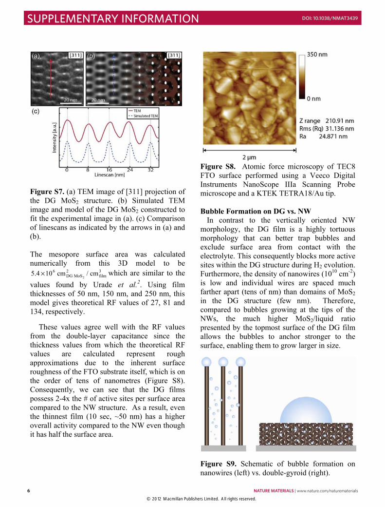
Long-term stability of DG MoS2 Films in Air
The 10 sec, 20 sec, and 1 min DG MoS2 films were left in air over a period of 4 months. XPS/XRD measurements were performed on these films, followed by resulphidization in
10%/90% H2S/H2 to revert any oxide back into a sulphide (Figures S12 and S13). The resulphidized films were then analysed using XPS/XRD (Figures S12 and S13), and re-assessed for electrochemical activity using cyclic voltammetry (Figure S14).
Figure S12. XPS of DG MoS2 films after 4 months of exposure to air (a and b), and following resulphidization in 10%/90% H2S/H2 (c and d).
9
Figure S13. XRD of DG MoS2 films after 4 months of exposure to air (a), and following resulphidization in 10%/90% H2S/H2 (b).
Figure S14. Initial electrochemical activity of DG MoS2 (1 min) (dark blue) and after 4 months (light blue) following resulphidization in 10%/90% H2S/H2.
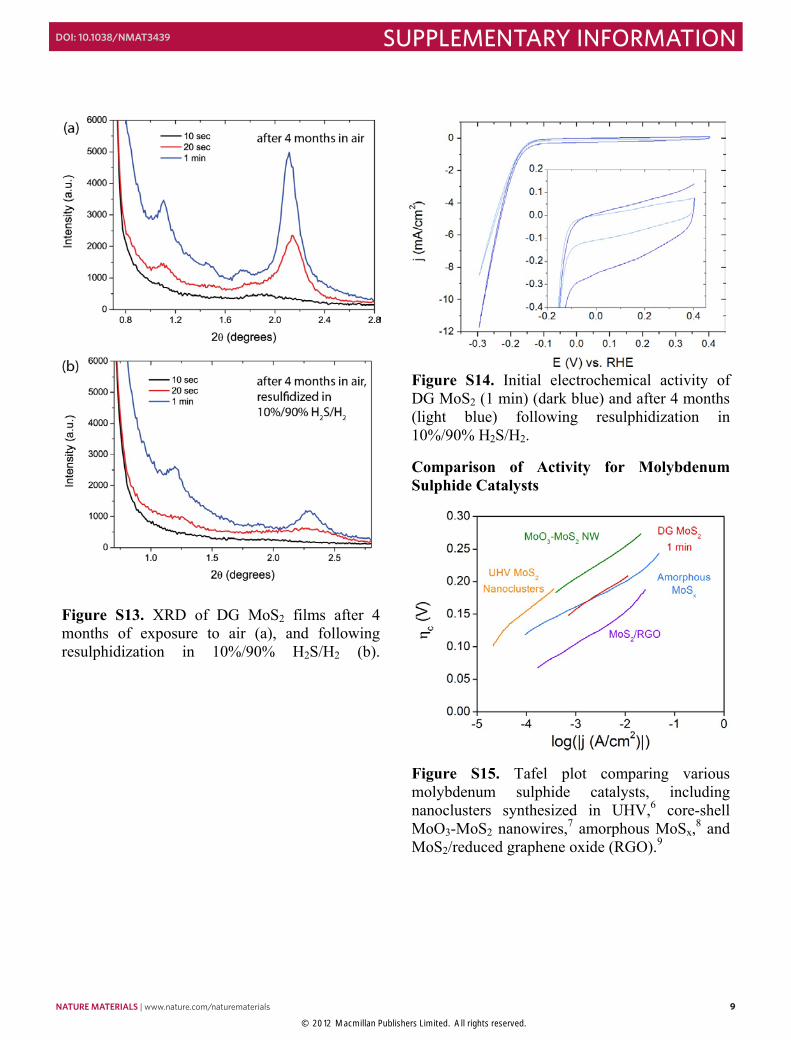
Comparison of Activity for Molybdenum Sulphide Catalysts
Figure S15. Tafel plot comparing various molybdenum sulphide catalysts, including nanoclusters synthesized in UHV,6 core-shell MoO3-MoS2 nanowires,7 amorphous MoSx,8 and MoS2/reduced graphene oxide (RGO).9
8 NATURE MATERIALS | www.nature.com/naturematerials
SUPPLEMENTARY INFORMATION DOI: 10.1038/NMAT3439
© 2012 Macmillan Publishers Limited. All rights reserved.
8
Long-term stability of DG MoS2 Films in Air
The 10 sec, 20 sec, and 1 min DG MoS2 films were left in air over a period of 4 months. XPS/XRD measurements were performed on these films, followed by resulphidization in
10%/90% H2S/H2 to revert any oxide back into a sulphide (Figures S12 and S13). The resulphidized films were then analysed using XPS/XRD (Figures S12 and S13), and re-assessed for electrochemical activity using cyclic voltammetry (Figure S14).
Figure S12. XPS of DG MoS2 films after 4 months of exposure to air (a and b), and following resulphidization in 10%/90% H2S/H2 (c and d).
9
Figure S13. XRD of DG MoS2 films after 4 months of exposure to air (a), and following resulphidization in 10%/90% H2S/H2 (b).
Figure S14. Initial electrochemical activity of DG MoS2 (1 min) (dark blue) and after 4 months (light blue) following resulphidization in 10%/90% H2S/H2.
Comparison of Activity for Molybdenum Sulphide Catalysts
Figure S15. Tafel plot comparing various molybdenum sulphide catalysts, including nanoclusters synthesized in UHV,6 core-shell MoO3-MoS2 nanowires,7 amorphous MoSx,8 and MoS2/reduced graphene oxide (RGO).9
NATURE MATERIALS | www.nature.com/naturematerials 9
SUPPLEMENTARY INFORMATIONDOI: 10.1038/NMAT3439
© 2012 Macmillan Publishers Limited. All rights reserved.

10
Sample Catalyst loading [μg/cm2]
j0
[A/cm2]
Tafel slope [mV/decade]
Amorphous MoSx 9 0.4-1.5×10⁻⁷ 40
MoS2/RGO 285 5.1×10⁻⁶ 41
DG 10 sec 10 1.3×10⁻⁷ 50
DG 20 sec 23 2.6×10⁻⁷ 50
DG 1 min 60 6.9×10⁻⁷ 50
Table S2. Comparison of catalyst loading, exchange current density, and Tafel slope between DG MoS2 vs. amorphous MoSx and MoS2/RGO catalysts as provided in a previous reference.10 The exchange current density for the MoS2/RGO was determined from the Tafel plot in Figure S15. Catalyst loadings for DG MoS2 were estimated based on charge passed during electrodeposition (Figure S2).
References
1. McEvoy, T.M. & Stevenson, K.J. Elucidation of the electrodeposition mechanism of molybdenum oxide from iso- and peroxo-polymolybdate solutions. J. Mater. Res. 19, 429-438 (2004).
2. Urade, V.N., Wei, T.C., Tate, M.P., Kowalski, J.D. & Hillhouse, H.W. Nanofabrication of double-gyroid thin films. Chem. Mat. 19, 768-777 (2007).
3. Tate, M.P., Urade, V.N., Gaik, S.J., Muzzillo, C.P. & Hillhouse, H.W. How to Dip-Coat and Spin-Coat Nanoporous Double-Gyroid Silica Films with EO19-PO43-EO19 Surfactant (Pluronic P84) and Know it Using a Powder X-ray Diffractometer. Langmuir 26, 4357-4367 (2010).
4. Conway, B.E., Birss, V. & Wojtowicz, J. The role and utilization of pseudocapacitance for energy storage by supercapacitors. J. Power Sources 66, 1-14 (1997).
5. Kotz, R. & Carlen, M. Principles and applications of electrochemical capacitors. Electrochim. Acta 45, 2483-2498 (2000).
6. Jaramillo, T.F. et al. Identification of active edge sites for electrochemical H2 evolution from MoS2 nanocatalysts. Science 317, 100-102 (2007).
7. Chen, Z. et al. Core–shell MoO3–MoS2 Nanowires for Hydrogen Evolution: A Functional Design for Electrocatalytic Materials. Nano Lett. (2011).
8. Merki, D., Fierro, S., Vrubel, H. & Hu, X. Amorphous molybdenum sulfide films as catalysts for electrochemical hydrogen production in water. Chemical Science 2, 1262-1267 (2011).
9. Li, Y. et al. MoS2 Nanoparticles Grown on Graphene: An Advanced Catalyst for the Hydrogen Evolution Reaction. J. Am. Chem. Soc. 133, 7296-7299 (2011).
10. Merki, D. & Hu, X. Recent developments of molybdenum and tungsten sulfides as hydrogen evolution catalysts. Energy & Environmental Science 4, 3878-3888 (2011).
10 NATURE MATERIALS | www.nature.com/naturematerials
SUPPLEMENTARY INFORMATION DOI: 10.1038/NMAT3439
© 2012 Macmillan Publishers Limited. All rights reserved.