Engineering Specification 15.0 inches SXGA+ Color … to contact IBM before proceeding with the...
26
Engineering Specification 15.0 inches SXGA+ Color TFT/LCD Module Model Name:ITSX93C Document Control Number : OEM93C-04 Note:Specification is subject to change without notice. Consequently it is better to contact to IBM before proceeding with the design of your product incorporating this module. Display Business Unit International Business Machines Corporation Engineering Specification (C) Copyright IBM Corp. 1999 All Rights reserved. August 27,1999 OEM93C-04 1/26
Transcript of Engineering Specification 15.0 inches SXGA+ Color … to contact IBM before proceeding with the...

Engineering Specification
15.0 inches SXGA+ Color TFT/LCD Module Model Name:ITSX93C
Document Control Number : OEM93C-04
Note:Specification is subject to change without notice. Consequently it is better to contact to IBMbefore proceeding with the design of your product incorporating this module.
Display Business UnitInternational Business Machines Corporation
Engineering Specification
(C) Copyright IBM Corp. 1999 All Rights reserved.
August 27,1999 OEM93C-04 1/26

i Contentsi Contentsii Record of Revision1.0 Handling Precautions 2.0 General Description2.1 Characteristics 2.2 Functional Block Diagram 3.0 Absolute Maximum Ratings4.0 Optical Characteristics5.0 Signal Interface5.1 Connectors5.2 Interface Signal Connector5.3 Interface Signal Description 5.4 Interface Signal Electrical Characteristics5.5 Signal for Lamp connector 6.0 Pixel format image7.0 Parameter guide line for CFL Inverter8.0 Interface Timings 8.1 Timing Characteristics8.2 Timing Definition9.0 Power Consumption10.0 Power ON/OFF Sequence11.0 Mechanical Characteristics
Engineering Specification
(C) Copyright IBM Corp. 1999 All Rights reserved.
August 27,1999 OEM93C-04 2/26

ii Record of Revision
To update DWGs for EMI solution.Based on Mechanical Drawing as of August 18,1999.
25 , 26OEM93C-04August 27,1999
To add an explanation for UL.To update White Luminance, Optical Rise Time/Fall Time,and Power consumption.To correct Absolute Maximum Rating For Shock.To update Optical Charastaristics.To correct Signal Name of Pin #15.To update LVDS Macro AC characteristics.To update White Luminance and CFL Ignition Voltage.To add a refference data.To update Timing Characteristics.To update Timing Definition.To update Power consumption.To update DWGs.Lamp cable length:95 mmBased on Internal Spec. as of June 22,1999.Based on Mechanical Drawing as of July 5,1999.
46
891116181920212325, 26
OEM93C-03July 9,1999
To update P/N for connector.7, 1027
OEM93C-02(Preliminary)
April 13,1999
First Edition for customer.Based on Initial Internal Spec. as of March 8,1999Based on Mechanical Drawing as of Draft March 3,1999.Updated information as of March 23.Lamp cable length:75.5 mm
AllOEM93C-01(Preliminary)
March 26,1999
SummaryPageDocumentRevision
Date
Engineering Specification
(C) Copyright IBM Corp. 1999 All Rights reserved.
August 27,1999 OEM93C-04 3/26
1.0 Handling Precautions 1) Since front polarizer is easily damaged, pay attention not to scratch it. 2) Be sure to turn off power supply when inserting or disconnecting from input connector. 3) Wipe off water drop immediately. Long contact with water may cause discoloration or spots. 4) When the panel surface is soiled, wipe it with absorbent cotton or other soft cloth. 5) Since the panel is made of glass, it may break or crack if dropped or bumped on hard surface. 6) Since CMOS LSI is used in this module, take care of static electricity and insure human earth when handling. 7) Do not open nor modify the Module Assembly. 8) Do not press the reflector sheet at the back of the module to any directions. 9) In case if a Module has to be put back into the packing container slot after once it was taken out from the container, do not press the center of the CFL Reflector edge. Instead, press at the far ends of the CFL Reflector edge softly. Otherwise the TFT Module may be damaged. 10) At the insertion or removal of the Signal Interface Connector, be sure not to rotate nor tilt the Interface Connector of the TFT Module. 11) After installation of the TFT Module into an enclosure ( Notebook PC Bezel, for example), do not twist nor bent the TFT Module even momentary. At designing the enclosure, it should be taken into consideration that no bending/twisting forces are applied to the TFT Module from outside. Otherwise the TFT Module may be damaged. 12)Small amount of materials having no flammability grade is used in the LCD module. The LCD module should be supplied by power complied with requirements of Limited Power Source (2.11, IEC60950 or UL1950), or be applied exemption conditions of flammability requirements (4.4.3.3, IEC60950 or UL1950) in an end product. 13)The LCD module is designed so that the CFL in it is supplied by Limited Current Circuit (2.4, IEC60950 or UL1950). Do not connect the CFL in Hazardous Voltage Circuit.
The information contained herein may be changed without prior notice. It is thereforeadvisable to contact IBM before proceeding with the design of equipment incorporating thisproduct.
y
The information contained herein is presented only as a guide for the applications of ourproducts. No responsibility is assumed by IBM for any infringements of patents or other rightof the third partied which may result from its use. No license is granted by implication orotherwise under any patent or patent rights of IBM or others.
y
Engineering Specification
(C) Copyright IBM Corp. 1999 All Rights reserved.
August 27,1999 OEM93C-04 4/26

2.0 General DescriptionThis specification applies to the 15.0 inches- Color TFT/LCD Module 'ITSX93C'. This module is designed for a display unit of notebook style personal computer. The screen format and electrical interface are intended to support the SXGA+(1400(H) x 1050(V)) screen.Support color is native 262K colors(RGB 6-bit data driver).All input signals are LVDS(Low Voltage Differential Signaling) interface compatible.This module does not contain an inverter card for backlight.
Engineering Specification
(C) Copyright IBM Corp. 1999 All Rights reserved.
August 27,1999 OEM93C-04 5/26

2.1 CharacteristicsThe following items are characteristics summary on the table under 25 ℃ condition:
0 to +50-20 to +60
Temperature Range [degree C]OperatingStorage (Shipping)
8 pairs LVDS(Even/Odd R/G/B Data(6bit), 3sync signals, Clock)Electrical Interface
4.6Typ.5.4MAX,(W/o inverter loss)6.0Typ.6.8MAX,(W/o inverter loss)
Typical Power Consumption [Watt](VDD Line + VCFL Line)Design Point 1:(ICFL=3.9mA)Design Point 2:(ICFL=6.5mA)
2.6Typ.,(W/o inverter loss)4.0Typ.,(W/o inverter loss)
Lamp Power Consumption [Watt](VCFL Line)Design Point 1:(ICFL=3.9mA)Design Point 2:(ICFL=6.5mA)
2.0 Typ.,2.8MAX.Power Consumption [Watt](VDD Line)
+3.3 Typ. Nominal Input Voltage VDD [Volt]
30Typ.,50 Max.Optical Rise Time/Fall Time [msec]
200 : 1 Typ. Contrast Ratio
90 Typ(center) 85 Typ(5 points average)150 Typ(center)140 Typ(5 points average)
White Luminance [cd/m2]Design Point 1:(ICFL=3.9mA)Design Point 2:(ICFL=6.5mA)
Native 262K colors(RGB 6-bit data driver)Support Color
Normally WhiteDisplay Mode
318.5(W) x 241.5(H) x 7.5(D) typ. Physical Size [mm]740Typ.Weight [grams]
R,G,B Vertical StripePixel Arrangement
0.2175(per one triad) x 0.2175Pixel Pitch [mm]
304.5(H) x 228.4(V)Active Area [mm]
1400(x3) x 1050Pixels H x V
381(15.0")Screen Diagonal [mm]
SPECIFICATIONSCHARACTERISTICS ITEMS
Engineering Specification
(C) Copyright IBM Corp. 1999 All Rights reserved.
August 27,1999 OEM93C-04 6/26

2.2 Functional Block DiagramThe following diagram shows the functional block of this 15.0 inches Color TFT/LCD Module.The first LVDS port transmits even pixels while the second LVDS port transmits odd pixels.
Engineering Specification
(C) Copyright IBM Corp. 1999 All Rights reserved.
August 27,1999 OEM93C-04 7/26
AMP 1318341-2 (30pin)
X-Driver
TFT ARRAY/CELL6bit color datafor R/G/B
DTCLK(even/odd)DSPTMG
HsyncVsync
VDD
LCDController
LCD DRIVECARD
Backlight Unit
1400(R/G/B) x 1050
GND
DC-DCConverterRef circuit
(even/odd)
< 8 pairs LVDS >
EVENPIXCEL
ODDPIXCEL
Dual LVDSRECEIVER
LCD-DRIVE Connector
Y-Driver
G/A
Lamp ConnectorJST BHSR-02VS-1 (2pin)

3.0 Absolute Maximum RatingsAbsolute maximum ratings of the module is as follows :
Rectangle waveG ms50 18ShockG Hz1.5 10-200Vibration
Note 1%RH955HSTStorage Relative HumidityNote 1℃+60-20TSTStorage TemperatureNote 1%RH958HOPOperating Relative HumidityNote 1℃+500TOPOperating Temperature
mA20-ICFLPCFL Peak Inrush CurrentmAms+7-ICFLCFL Current
Note 2Vrms+1,600-VsCFL Ignition VoltageVVDD+0.3-0.3VINInput Signal VoltageV+4.0-0.3VDDLogic/LCD Drive Voltage
Conditions Unit Max MinSymbol Item
Note 1 : Maximum Wet-Bulb should be 39℃℃℃℃ and No condensation.Note 2 : Duration : 50msec Max. Ta=0 ℃℃℃℃
Engineering Specification
(C) Copyright IBM Corp. 1999 All Rights reserved.
August 27,1999 OEM93C-04 8/26

4.0 Optical CharacteristicsThe optical characteristics are measured under stable conditions as follows under 25℃ condition:
-150Typ.(TBD)
Center140Typ.(TBD)
5 pointsaverage
White Luminance (cd/㎡)ICFL 6.5 mA
+-0.0300.346White y+-0.0300.310White x+-0.0400.157Blue y+-0.0300.158Blue x+-0.0300.563Green y+-0.0300.310Green x(CIE)+-0.0300.338Red yChromaticity+-0.0400.577Red xColor 50Max30Falling(ms)50Max30RisingResponse Time
-200Contrast ratio
--
1530
Vertical (Upper)KP10 (Lower)K:Contrast Ratio
--
4040
Horizontal (Right) KP10 (Left)
Viewing Angle (Degrees)
NoteTyp.SpecificationConditionsItem
Engineering Specification
(C) Copyright IBM Corp. 1999 All Rights reserved.
August 27,1999 OEM93C-04 9/26

5.0 Signal Interface5.1 ConnectorsPhysical interface is described as for the connector on module.These connectors are capable of accommodating the following signals and will be following components.
1318335-2Mating Receptacle/Part Number
AMPMating Receptacle Manufacture
1318341-2Type / Part Number
AMPManufacturer
For Signal ConnectorConnector Name / Designation
SM02B-BHSS-1Mating Type / Part Number
BHSR-02VS-1Type / Part Number
JSTManufacturer
For Lamp ConnectorConnector Name / Designation
Engineering Specification
(C) Copyright IBM Corp. 1999 All Rights reserved.
August 27,1999 OEM93C-04 10/26

5.2 Interface Signal Connector
Reserved30ReCLKIN-15GND29GND14RoCLKIN+28ReIN2+13RoCLKIN-27ReIN2-12GND26GND11RoIN2+25ReIN1+10RoIN2-24ReIN1-9GND23GND8RoIN1+22ReIN0+7RoIN1-21ReIN0-6GND20GND5RoIN0+19GND4RoIN0-18VDD3GND17VDD2ReCLKIN+16VDD1Signal NamePin #Signal NamePin #
Note: 'Reserved' pins are not allowed to connect any other line. Voltage levels of all input signals are LVDS compatible (except VDD). Refer to 5.4 " Interface Signal Electrical Characteristics", for voltage levels of all input signals.
Engineering Specification
(C) Copyright IBM Corp. 1999 All Rights reserved.
August 27,1999 OEM93C-04 11/26
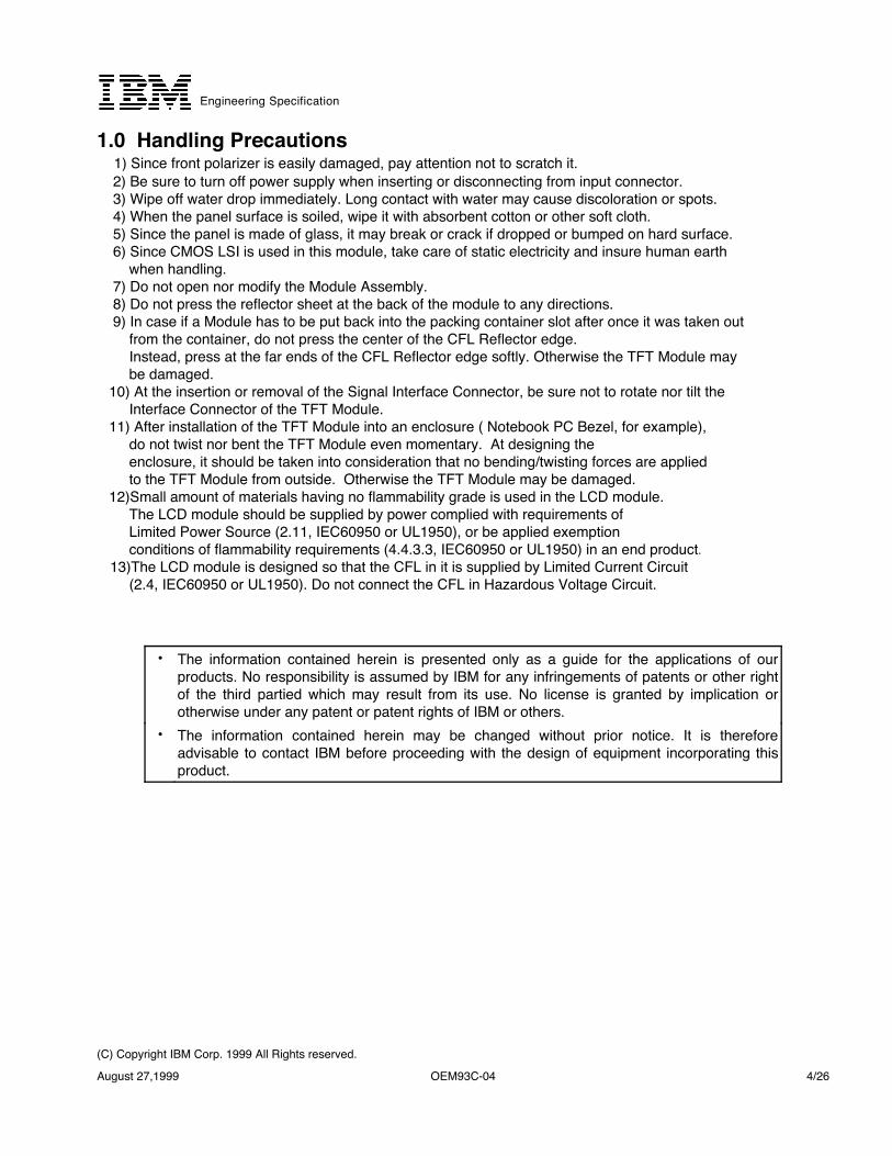
5.3 Interface Signal Description
The module uses a pair of LVDS receiver SN75LVDS86(Texas Instruments) compatible. LVDS is a differentialsignal technology for LCD interface and high speed data transfer device. Transmitter shall be SN75LVDS84/85or compatible.
ReservedReserved30GroundGND29Positive LVDS differential clock input (Odd)RoCLKIN+28Negative LVDS differential clock input (Odd)ReCLKIN-27GroundGND26Positive LVDS differential data input (Odd B2-B5)RoIN2+25Negative LVDS differential data input (Odd B2-B5)RoIN2-24GroundGND23Positive LVDS differential data input (Odd G1-G5, B0-B1)RoIN1+22Negative LVDS differential data input (Odd G1-G5, B0-B1)RoIN1-21Ground GND20Positive LVDS differential data input (Odd R0-R5, G0)RoIN0+19Negative LVDS differential data input (Odd R0-R5, G0)RoIN0-18GroundGND17Positive LVDS differential clock input (Even)ReCLKIN+16Negative LVDS differential clock input (Even)ReCLKIN-15GroundGND14Positive LVDS differential data input (Even B2-B5, HSYNC, VSYNC, DSPTMG)ReIN2+13Negative LVDS differential data input (Even B2-B5, HSYNC, VSYNC, DSPTMG)ReIN2-12Ground GND11Positive LVDS differential data input (Even G1-G5, B0-B1)ReIN1+10Negative LVDS differential data input (Even G1-G5, B0-B1)ReIN1-9Ground GND8Positive LVDS differential data input (Even R0-R5, G0)ReIN0+7Negative LVDS differential data input (Even R0-R5, G0)ReIN0-6Ground GND5Ground GND4VDD (+3.3V)VDD3VDD (+3.3V)VDD2VDD (+3.3V)VDD1
Description SIGNALNAME
PIN#
Note:'Reserved' pin is not allowed to connect any other line. Output signals from any system shall be Hi-Z state when VDD is off. Input signals of odd and even clock shall be the same timing.
Engineering Specification
(C) Copyright IBM Corp. 1999 All Rights reserved.
August 27,1999 OEM93C-04 12/26

Internal circuit of LVDS inputs are as follows.
(26)D1(27)D2(29)D3(30)D4(31)D5(33)D6(34)D7(35)D8(37)D9(39)D10(40)D11(41)D12(43)D13(45)D14(46)D15(47)D16(1)D17(2)D18(4)D19(5)D20
(24)D0 Even +Red 0Even +Red 1Even +Red 2Even +Red 3Even +Red 4Even +Red 5 Even +Green 0Even +Green 1Even +Green 2Even +Green 3Even +Green 4Even +Green 5 Even +Blue 0Even +Blue 1Even +Blue 2Even +Blue 3Even +Blue 4Even +Blue 5 HSYNCVSYNCDSPTMG
A0P(9)
A1M(10)
A1P(11)
A2M(14)
A2P(15)
CLKINM(16)
CLKINP(17)
(23)CLKOUT EVEN DTCLK
R
R
R
R
A0M(8)ReIN0-
ReIN0+
ReIN1-
ReIN1+
ReIN2-
ReIN2+
ReCLKIN-
ReCLKIN+
7
9
10
12
13
15
16
SN75LVDS86 CompatibleSignal Input
Pin No.
6
LVDS GND(7,13,18)LVDS GND,PLL GND
0 ohm Jumper
Return/GND4,5,8,11,14,17,20,23,26,29
PLL GND(19,21)
I/F Connector Frame Shell (FG)
0 ohm Jumper
GND
The module uses a 100ohm resistor between positive and negative data lines of each receiver input.
Engineering Specification
(C) Copyright IBM Corp. 1999 All Rights reserved.
August 27,1999 OEM93C-04 13/26

(26)D1(27)D2(29)D3(30)D4(31)D5(33)D6(34)D7(35)D8(37)D9(39)D10(40)D11(41)D12(43)D13(45)D14(46)D15(47)D16(1)D17(2)D18(4)D19(5)D20
(24)D0 Odd +Red 0Odd +Red 1Odd +Red 2Odd +Red 3Odd +Red 4Odd +Red 5 Odd +Green 0Odd +Green 1Odd +Green 2Odd +Green 3Odd +Green 4Odd +Green 5 Odd +Blue 0Odd +Blue 1Odd +Blue 2Odd +Blue 3Odd +Blue 4Odd +Blue 5 NCNCNC
A0P(9)
A1M(10)
A1P(11)
A2M(14)
A2P(15)
CLKINM(16)
CLKINP(17)
(23)CLKOUT ODD DTCLK
R
R
R
R
A0M(8)RoIN0-
RoIN0+
RoIN1-
RoIN1+
RoIN2-
RoIN2+
RoCLKIN-
RoCLKIN+
19
21
22
24
25
27
28
Signal Input
Pin No.
18
LVDS GND(7,13,18)
0 ohm Jumper
Return/GND 4,5,8,11,14,17,20,23,26,29
PLL GND(19,21)
I/F Connector Frame Shell (FG)
0 ohm Jumper
GND
LVDS GNDPLL GND
SN75LVDS86 Compatible
The module uses a 100ohm resistor between positive and negative lines of each receiver input.
Engineering Specification
(C) Copyright IBM Corp. 1999 All Rights reserved.
August 27,1999 OEM93C-04 14/26

Ground GND+3.3V Power SupplyVDD
Horizontal Sync: This signal is synchronized with -DTCLK. Both active high/low signals areacceptable.
HSYNC
Vertical Sync: This signal is synchronized with -DTCLK. Both active high/low signals areacceptable.
VSYNCWhen the signal is high, the pixel data shall be valid to be displayed.Display Timing:+DSPTMGThe signal is used to strobe the pixel +data and the +DSPTMG (EVEN/ODD)
Data Clock: The typical frequency is 54MHz.-DTCLKBlue-pixel Data: Each blue pixel's brightness data consists of these 6 bits pixel data.
(EVEN/ODD)BLUE Data 0 (LSB)+BLUE 0BLUE Data 1+BLUE 1BLUE Data 2+BLUE 2BLUE Data 3+BLUE 3BLUE Data 4+BLUE 4BLUE Data 5 (MSB)+BLUE 5Green-pixel Data: Each green pixel's brightness data consists of these 6 bits pixel data.
(EVEN/ODD)GREEN Data 0 (LSB)+GREEN 0GREEN Data 1+GREEN 1GREEN Data 2+GREEN 2GREEN Data 3+GREEN 3GREEN Data 4+GREEN 4GREEN Data 5 (MSB)+GREEN 5Red-pixel Data: Each red pixel's brightness data consists of these 6 bits pixel data.
(EVEN/ODD)RED Data 0 (LSB)+RED 0RED Data 1+RED 1RED Data 2+RED 2RED Data 3+RED 3RED Data 4+RED 4RED Data 5 (MSB)+RED 5Description (ITSX93)SIGNAL NAME
Note: Output signals from any system shall be Hi-Z state when VDD is off.
Engineering Specification
(C) Copyright IBM Corp. 1999 All Rights reserved.
August 27,1999 OEM93C-04 15/26

5.4 Interface Signal Electrical Characteristics
Input signals shall be low or Hi-Z state when VDD is off.It is recommended to refer the specifications of SN75LVDS86DGG(Texas Instruments) in detail.
Signal electrical characteristics are as follows;
mV-100Differential Input High Voltage (Vcm=+1.2V)
Vtl
mV100Defferential Input High Voltage (Vcom=+1.2V)
Vth
unit Max Min ConditionParameter
LVDS Macro AC characteristics are as follows:
ps800 MinData Hold Time (Thd) ps800 MinData Setup Time (Tsu)
MHz54 Typ.Clock Frequency (T)UnitValue
Input Clock
Input Data
Tsu Thd
T
5.5 Signal for Lamp Connector
Lamp Low Voltage 2
Lamp High Voltage1
Signal NamePin #
Engineering Specification
(C) Copyright IBM Corp. 1999 All Rights reserved.
August 27,1999 OEM93C-04 16/26

6.0 Pixel format image
Following figure shows the relationship of the input signals and LCD pixel format image. Even and odd pair ofRGB data are sampled at a time.
R G B R G B
R G B R G B
R G B R G B
R G B R G B
Even Odd Even Odd 0 1 1399
1st Line
1050th Line
1398
Engineering Specification
(C) Copyright IBM Corp. 1999 All Rights reserved.
August 27,1999 OEM93C-04 17/26

7.0 Parameter guide line for CFL Inverter
(Ta=25℃)Note 2
W-42.6-CFL Power consumption(PCFL)
(Ta=25℃)Note 2
Vrms-610675-CFL Voltage (Reference)(VCFL)
(Ta= 0℃)Note 3
Vrms---1,450CFL Ignition Voltage(Vs)
(Ta=25℃)Note 1
KHz60505040CFL Frequency(FCFL)
(Ta=25℃)mArms7.06.53.93.0CFL current(ICFL)
(Ta=25℃)cd/㎡--
150140
9085
--
White Luminance(Center)(5 Points average)
CONDITIONUNITSMAXDP-2DP-1 MINPARAMETER
Note 1: CFL discharge frequency should be carefully determined to avoid interference between inverter and TFTLCD.
Note 2: Calculated value for reference (ICFL x VCFL = PCFL).Note 3: CFL inverter should be able to give out a power that has a generating capacity of over 1,450 voltage. Lamp units need 1,450 voltage minimum for ignition.Note 4: DP-1 and DP-2 are IBM recommended Design Points. *1 All of characteristics listed are measured under the condition using the IBM Test inverter. *2 In case of using an inverter other than listed, it is recommended to check the inverter carefully. Sometimes, interfering noise stripes appear on the screen, and substandard luminance or flicker at low power may happen. *3 In designing an inverter, it is suggested to check safety circuit very carefully. Impedance of CFL, for instance, becomes more than 1 [M ohm] when CFL is damaged. *4 Generally, CFL has some amount of delay time after applying kick-off voltage. It is recommended to keep on applying kick-off voltage for 1 [Sec] until discharge. *5 CFL discharge frequency must be carefully chosen so as not to produce interfering noise stripes on the screen. *6 Reducing CFL current increases CFL discharge voltage and generally increases CFL discharge frequency. So all the parameters of an inverter should be carefully designed so as not to produce too much leakage current from high-voltage output of the inverter.
Engineering Specification
(C) Copyright IBM Corp. 1999 All Rights reserved.
August 27,1999 OEM93C-04 18/26
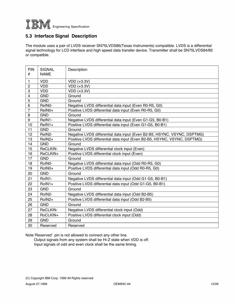
The following chart is CFL current versus the luminance for your reference.
Engineering Specification
(C) Copyright IBM Corp. 1999 All Rights reserved.
August 27,1999 OEM93C-04 19/26

8.0 Interface Timings Basically, interface timings described here is not actual input timing of LCD module but output timing ofSN75LVDS86(Texas Instruments) or equivalent.
8.1 Timing Characteristics
[dots]1400nData Even/Odd+DATA
[usec]12.96ThdDisplay+DSPTMG
[Tck]248ThfH-Front Porch
[Tck]648ThbH-Back Porch
[Tck]5610Tha
[usec]1.037ThaH-Active Level
[Tck]1023844820Nh
[usec]15.63Th
[kHz]69.5163.98FhScan Rate+H-Sync
[lines]1050mV-Line+DSPTMG
[lines]11NvfV-Front Porch
[lines]63127NvbV-Back Porch
[lines]31Nva
[us]46.715.78TvaV-Active Level
[lines]204710661059Nv
[ms]17.7816.6716.39Tv
[Hz](61)60(56.25)FvFrame Rate+V-Sync
[ns]18.517.5Tck
[MHz]6054FdckFreqencyDTCLK
UnitMAX.TYP.MIN.SymbolItemSignal
Note:1. Tha+Thb should be less than 1024.2. Both positive Hsync and positive Vsync polarity is recommended.
Engineering Specification
(C) Copyright IBM Corp. 1999 All Rights reserved.
August 27,1999 OEM93C-04 20/26

8.2 Timing Definition
Vertical Timing
0.188 ms(12 lines)
0.047 ms(3 lines)
16.661 ms(1066lines)
0.016 ms(1 line)
16.411 ms(1050lines)
0.250 ms(16 lines)
1400 x 1050 at 60Hz(H line rate : 15.63us)
Tvb VSYNCBack Porch
Tva VSYNCWidth
Tv,NvFrame Time
Tvf VSYNCFrontPorch
m ActiveField
TvblkVerticalBlanking
Support mode
Tvblk mTvf Tva Tvb
TvDSPTMG
-VSYNC
+VSYNC
Horizontal Timing
1.185 us(128 dots)
1.037 us(112 dots)
15.630 us(1688dots)
0.444 us(48 dots)
12.963 us(1400dots)
2.667 us(288 dots)
1400 x 1050 Dotclock : 108.000MHz (54.000MHz x2)
Thb HSYNCBack Porch
Tha HSYNCWidth
Th,Nh H LineTime
Thf HSYNCFrontPorch
Thd ActiveField
Thblk Horizontal Blanking
Support mode
Thblk ThdThf Tha Thb
ThDSPTMG
-HSYNC
+HSYNC
Engineering Specification
(C) Copyright IBM Corp. 1999 All Rights reserved.
August 27,1999 OEM93C-04 21/26

VSYNC
HSYNC
DSPTMG
TvTva
Th Tha
Tvb Tvf
1 2 3 m
Vsync,Hsync and Display Timing
VIDEO(EVEN)
VIDEO(ODD)
DOTCLK
DSPTMG
HSYNC
Thd
Thd
Tck
Tck
Tha Thb Thf
Video signal and Dot clock
0
1
2
3
n-4
n-3
n-2
n-1
Engineering Specification
(C) Copyright IBM Corp. 1999 All Rights reserved.
August 27,1999 OEM93C-04 22/26

9.0 Power ConsumptionInput power specifications are as follows;
mVp-p100Allowable Logic/LCDDrive Ripple Noise
VDDns
mVp-p100Allowable Logic/LCDDrive Ripple Voltage
VDDrp
All Black PatternVDD=3.3V
mA600IDD Current IDD
MAX PatternVDD=3.0V
mA85IDD Current MaxIDD Max
All Black PatternVDD=3.3V
W2VDD PowerPDD
MAX Pattern VDD=3.6V
W2.8VDD Power MaxPDD
Load Capacitance 30uFV3.63.33Logic/LCD DriveVoltage
VDDCONDITIONUNITSMaxTypMinPARAMETERSYMBOL
Note:Max Pattern:2 dot Vertical sub-pixel stripe.
Engineering Specification
(C) Copyright IBM Corp. 1999 All Rights reserved.
August 27,1999 OEM93C-04 23/26

10.0 Power ON/OFF SequenceVDD power and lamp on/off sequence is as follows. Interface signals are also shown in the chart. Signals fromany system shall be Hi-Z state or low level when VDD is off.
90%
10%
10% 10%
90%
10ms max.
0 min. 0 min.
0 V
0 V
VDD
Signals
10% 10%
180ms min. 0 min.
0 V
Lamp On(Recommended)
10% 10%
150ms min.
Engineering Specification
(C) Copyright IBM Corp. 1999 All Rights reserved.
August 27,1999 OEM93C-04 24/26

11.0 Mechanical Characteristics
Engineering Specification
(C) Copyright IBM Corp. 1999 All Rights reserved.
August 27,1999 OEM93C-04 25/26

****** End Of Page ******
Engineering Specification
(C) Copyright IBM Corp. 1999 All Rights reserved.
August 27,1999 OEM93C-04 26/26