Engineering nonlinearities in nanoscale optical systems ...npanoiu/documents/opd09aop.pdf ·...
74
Engineering nonlinearities in nanoscale optical systems: physics and applications in dispersion-engineered silicon nanophotonic wires R. M. Osgood, Jr., 1 N. C. Panoiu, 2 J. I. Dadap, 1 Xiaoping Liu, 1 Xiaogang Chen, 1 I-Wei Hsieh, 1 E. Dulkeith, 3,4 W. M. J. Green, 3 and Y. A. Vlasov 3 1 Microelectronics Sciences Laboratories, Columbia University, NewYork, NewYork 10027, USA 2 Department of Electronic and Electrical Engineering, University College London, Torrington Place, London WC1E 7JE, UK 3 IBMT. J. Watson Research Center,Yorktown Heights, NewYork 10598, USA 4 Present address, Detecon, Inc., Strategy and Innovation Engineering Group, San Mateo, California 94402, USA Received October 7, 2008; revised November 24, 2008; accepted November 25, 2008; posted November 25, 2008 (Doc. ID 102501); published January 30, 2009 The nonlinear optics of Si photonic wires is discussed. The distinctive features of these waveguides are that they have extremely large third-order susceptibility 3 and dispersive properties. The strong dispersion and large third-order nonlinearity in Si photonic wires cause the linear and nonlinear optical physics in these guides to be intimately linked. By carefully choosing the waveguide dimensions, both linear and nonlinear optical properties of Si wires can be engineered. We review the fundamental optical physics and emerging applications for these Si wires. In many cases, the relatively low threshold powers for nonlinear optical effects in these wires make them potential candidates for functional on-chip nonlinear optical devices of just a few millimeters in length; conversely, the absence of nonlinear optical impairment is important for the use of Si wires in on-chip interconnects. In addition, the characteristic length scales of linear and nonlinear optical effects in Si wires are markedly different from those in commonly used optical guiding systems, such as optical fibers or photonic crystal fibers, and therefore guiding structures based on Si wires represent ideal optical media for investigating new and intriguing physical phenomena. OCIS codes: 190.4390, 130.4310, 190.7110, 060.5060, 130.2790, 230.3990, 230.7370. 1. Introduction............................................... 164 1.1. Introductory Remarks.................................... 164 Advances in Optics and Photonics 1, 162–235 (2009) doi:10.1364/AOP.1.000162 162 © 2009 Optical Society of America
Transcript of Engineering nonlinearities in nanoscale optical systems ...npanoiu/documents/opd09aop.pdf ·...

Eoas
RXY1
N
2
T
3
4
S
Rp
1
A
©
ngineering nonlinearities in nanoscaleptical systems: physics andpplications in dispersion-engineered
ilicon nanophotonic wires
. M. Osgood, Jr.,1 N. C. Panoiu,2 J. I. Dadap,1 Xiaoping Liu,1
iaogang Chen,1 I-Wei Hsieh,1 E. Dulkeith,3,4 W. M. J. Green,3 and. A. Vlasov3
Microelectronics Sciences Laboratories, Columbia University, New York,ew York 10027, USA
Department of Electronic and Electrical Engineering, University College London,orrington Place, London WC1E 7JE, UK
IBM T. J. Watson Research Center, Yorktown Heights, New York 10598, USA
Present address, Detecon, Inc., Strategy and Innovation Engineering Group,an Mateo, California 94402, USA
eceived October 7, 2008; revised November 24, 2008; accepted November 25, 2008;osted November 25, 2008 (Doc. ID 102501); published January 30, 2009
The nonlinear optics of Si photonic wires is discussed. The distinctive featuresof these waveguides are that they have extremely large third-ordersusceptibility ��3� and dispersive properties. The strong dispersion and largethird-order nonlinearity in Si photonic wires cause the linear and nonlinearoptical physics in these guides to be intimately linked. By carefully choosingthe waveguide dimensions, both linear and nonlinear optical properties ofSi wires can be engineered. We review the fundamental optical physics andemerging applications for these Si wires. In many cases, the relativelylow threshold powers for nonlinear optical effects in these wires make thempotential candidates for functional on-chip nonlinear optical devices of just afew millimeters in length; conversely, the absence of nonlinear opticalimpairment is important for the use of Si wires in on-chip interconnects. Inaddition, the characteristic length scales of linear and nonlinear optical effectsin Si wires are markedly different from those in commonly used opticalguiding systems, such as optical fibers or photonic crystal fibers, and thereforeguiding structures based on Si wires represent ideal optical media forinvestigating new and intriguing physical phenomena.
OCIS codes: 190.4390, 130.4310, 190.7110, 060.5060, 130.2790, 230.3990,230.7370.
. Introduction. . . . . . . . . . . . . . . . . . . . . . . . . . . . . . . . . . . . . . . . . . . . . . . 164
1.1. Introductory Remarks. . . . . . . . . . . . . . . . . . . . . . . . . . . . . . . . . . . . 164dvances in Optics and Photonics 1, 162–235 (2009) doi:10.1364/AOP.1.000162 162
2009 Optical Society of America

2
3
4
5
6
7
8AAAR
A
©
1.2. Scope of This Review. . . . . . . . . . . . . . . . . . . . . . . . . . . . . . . . . . . . 167. Si Photonic Wires: Optical Characterization and Dispersive
Properties. . . . . . . . . . . . . . . . . . . . . . . . . . . . . . . . . . . . . . . . . . . . . . . . . 1672.1. Si Photonic Wires and Their Optical Characterization. . . . . . . . . . . 1682.2. Dispersion Engineering in Si Photonic Wires. . . . . . . . . . . . . . . . . 169
2.2a. Introduction. . . . . . . . . . . . . . . . . . . . . . . . . . . . . . . . . . . . . . . 1692.2b. Dispersion in Si Nanophotonic Wires. . . . . . . . . . . . . . . . . . . 1692.2c. Dispersion Control for Nonlinear Waveguide Optics. . . . . . . 1722.2d. Active Control of Birefringence. . . . . . . . . . . . . . . . . . . . . . . 174
. Basic Parameters of Nonlinear Optics in Crystalline Si. . . . . . . . . . . . . 1743.1. Basic Nonlinear Optical Physics in Si. . . . . . . . . . . . . . . . . . . . . . . 1743.2. Raman Response. . . . . . . . . . . . . . . . . . . . . . . . . . . . . . . . . . . . . . . . 1783.3. Effective Nonlinear Susceptibility in Si Photonic Wires. . . . . . . . . 1793.4. Carrier Dynamics in Si Photonic Wires. . . . . . . . . . . . . . . . . . . . . . 180
. Theory of Nonlinear Optical Pulse Propagation and Dynamics in SiPhotonic Wires. . . . . . . . . . . . . . . . . . . . . . . . . . . . . . . . . . . . . . . . . . . . . 1814.1. Theory of Light Propagation in Si Photonic Wires. . . . . . . . . . . . . 1814.2. Coupled-Mode Equations for Multifrequency Pulse Propagation.. 1844.3. Effects of Strong Optical Confinement on Optical Nonlinearity. . . 1864.4. Frequency Dispersion of the Effective Optical Nonlinearity of Si
Photonic Wires. . . . . . . . . . . . . . . . . . . . . . . . . . . . . . . . . . . . . . . . . 1874.5. Characteristic Lengths in Si Photonic Wires versus Optical
Fibers. . . . . . . . . . . . . . . . . . . . . . . . . . . . . . . . . . . . . . . . . . . . . . . . 1894.6. Higher-Order Linear and Nonlinear Optical Effects in Si
Photonic Wires: Solitons and Wire Dispersion. . . . . . . . . . . . . . . . . 1904.6a. Third-Order Dispersion Effects. . . . . . . . . . . . . . . . . . . . . . . . 1904.6b. Self-Steepening. . . . . . . . . . . . . . . . . . . . . . . . . . . . . . . . . . . . 193
. Experimental Observations of Raman Amplification. . . . . . . . . . . . . . . . 1975.1. Raman Amplification. . . . . . . . . . . . . . . . . . . . . . . . . . . . . . . . . . . . 1975.2. Removal of Photogenerated Carriers. . . . . . . . . . . . . . . . . . . . . . . . 199
. Observations of Optical Nonlinearities in Si Wires. . . . . . . . . . . . . . . . . 2006.1. Optical Limiting. . . . . . . . . . . . . . . . . . . . . . . . . . . . . . . . . . . . . . . . 2006.2. Self-Phase Modulation and Third-Order Dispersion. . . . . . . . . . . . 2026.3. Soliton Generation. . . . . . . . . . . . . . . . . . . . . . . . . . . . . . . . . . . . . . 2046.4. Cross-Phase Modulation. . . . . . . . . . . . . . . . . . . . . . . . . . . . . . . . . . 2056.5. Parametric Processes: Frequency Mixing. . . . . . . . . . . . . . . . . . . . . 2086.6. Tunability of Four-Wave Mixing. . . . . . . . . . . . . . . . . . . . . . . . . . . 2116.7. Free-Carrier Control. . . . . . . . . . . . . . . . . . . . . . . . . . . . . . . . . . . . . 2126.8. Modulation Instability. . . . . . . . . . . . . . . . . . . . . . . . . . . . . . . . . . . 213
. Applications of Nonlinearities in Si Nanowires. . . . . . . . . . . . . . . . . . . . 2147.1. Continuum Generation. . . . . . . . . . . . . . . . . . . . . . . . . . . . . . . . . . . 2157.2. Spectral Manipulation of Pulses Using Si Photonic Wires. . . . . . . . 2177.3. Signal Regeneration Using Four-Wave Mixing. . . . . . . . . . . . . . . . 2187.4. On-Chip Data Communication. . . . . . . . . . . . . . . . . . . . . . . . . . . . . 2197.5. Broadband Wavelength Conversion of High-Data-Rate Signals. . . 2207.6. Raman Pulse Delay. . . . . . . . . . . . . . . . . . . . . . . . . . . . . . . . . . . . . . 220
. Conclusion. . . . . . . . . . . . . . . . . . . . . . . . . . . . . . . . . . . . . . . . . . . . . . . . 221ppendix A: Acronym Glossary. . . . . . . . . . . . . . . . . . . . . . . . . . . . . . . . . . 222ppendix B: Symbol Glossary. . . . . . . . . . . . . . . . . . . . . . . . . . . . . . . . . . . 223cknowledgments. . . . . . . . . . . . . . . . . . . . . . . . . . . . . . . . . . . . . . . . . . . . . 226eferences. . . . . . . . . . . . . . . . . . . . . . . . . . . . . . . . . . . . . . . . . . . . . . . . . . . 226
dvances in Optics and Photonics 1, 162–235 (2009) doi:10.1364/AOP.1.000162 163
2009 Optical Society of America

Eoas
RXY
1
1
Nuostaco
Ivtcpahmhwcbpp[
Mvdnmms
A
©
ngineering nonlinearities in nanoscaleptical systems: physics andpplications in dispersion-engineered
ilicon nanophotonic wires
. M. Osgood, Jr., N. C. Panoiu, J. I. Dadap, Xiaoping Liu,iaogang Chen, I-Wei Hsieh, E. Dulkeith, W. M. J. Green, and. A. Vlasov
. Introduction
.1. Introductory Remarks
onlinear optics is one of the major successes of modern optics. Practicaltilization of nonlinear optical processes and in most cases even the simplebservation of the phenomena relies on high-intensity near-monochromatic lightources and control of phase and coherence in the optical system; both ofhese capabilities are now available thanks to laser sources. Nonlinear optics islso eminently practical, with hundreds of applications being pursued in theommercial arena, including wavelength converters for telecommunications,ptical signal processing, and optical switching.
n the past decade, major advances in our ability to pattern and fabricate aariety of materials have led to the focusing of research in nonlinear optics onhe topic of nanoscale nonlinear optic methods. However, despite itsontemporary name, nanoscale nonlinear optics has a long and distinguishedast! This is well illustrated by the early use of optical frequency mixingt the ångstrom-dimension tip of point contact diodes [1]. In fact this approachas recently been revived in the use of the surfaces of scanning tunnelingicroscope tips to enhance nonlinear optics for local generation of optical higher
armonics [2]. In addition the need to make integrated optical structures,hich enable efficient phase matching by using artificial periodic media, is
learly a micrometer-scale precursor to today’s nanoscale nonlinear optics. Theest example of this approach is the progress in making periodic-domainoled LiNbO3 (PPLN) structures [3]. In fact, these structures have recently beenushed to nanoscale dimensions by using two-dimensional poling methods4].
ore recently, research in nonlinear nano-optical phenomena has taken twoery different directions. The first has used the excitement in metamaterials toevelop a new, generally metal-film-based approach to driving strongonlinearities in metals and metallodielectric materials [5–8]. Typically thisetamaterials approach uses a surface normal configuration. Theseetallodielectric nanostructures can make nonlinear optical conversion at a
maller scale and broader band, with a lower optical loss. Metamaterials can also
dvances in Optics and Photonics 1, 162–235 (2009) doi:10.1364/AOP.1.000162 164
2009 Optical Society of America

gtbppiucnasCna
Toati[m[coftfctbcpeta
Tprsowfss[edaoa[
A
©
ive more flexibility in wavelength range via the choice of the dimensions ofhe nanostructure metal array and its selection of materials. This approach haseen examined for important potential applications in optical signalrocessing; however the focus has generally been on investigating new opticalhysics. The second direction has examined in-plane optical nonlinearitiesn dielectric structures with nanometer-scale cross sections. In this case, thesual guided-wave nonlinearities are generated in a structure, which alsoontrols to all orders the optical dispersion of the guiding structure. Theonlinearities are sufficiently large that the waveguides act in the same manners they do in optical fibers—but since the structures are of chip scale, theirubwavelength characteristics strongly affect their optical properties.onsequently, both new physical and new optical phenomena are present, andearer-term applications are apparent. These high-confinement Si devicesre a natural complement to fiber optic guided-wave interconnect systems.
his second nano-optical approach, which is the subject of this review, is basedn the recent advances in developing the area of active Si photonics devicesnd understanding their underlying physics. This area of research began morehan two decades ago by using clearly nonnanoscale devices based on thedeas of Soref and Lorenzo, in which the first Si waveguide was demonstrated9]. Soon after, work in active Si photonics focused on realizing electro-opticalodulators, through the use of free carriers, e.g., by carrier injection,
10–14], and thermo-optic modulators, by using the favorable thermo-opticoefficient of Si [15–19]. An important goal for these modulators, as well as forther Si optical passive and active devices, is scaling down the deviceootprint and power consumption and increasing the frequency response so aso allow for full integration with Si electronics. In fact, because of theavorable electronic, optical, and physical properties of Si and the matureomplementary metal-oxide-semiconductor (CMOS) fabrication processingechnology, large-scale integration of functional optical devices hasecome possible, including integration with relatively complex electronicomponents. The use of CMOS manufacturing [20] also facilitates its preciseatterning to be applied to integrated optical circuits; this enables, forxample, greatly reduced sidewall roughness and, hence, very low loss even inhe small waveguides mentioned here. The rapid growth of Si photonics haslready generated several excellent review articles and books [21–39].
his work in active devices has led to increasing interest in nonlinear Sihotonics. Generally speaking this interest stems from two separate but relatedesearch goals: the development of all-optical control of dramaticallycaled-down optical devices and the interest in small-dimension waveguides asn-chip transport light guides. In the latter case, one of course primarilyishes to minimize nonlinear effects, although they could have an important
unctionality in applications such as light amplification or on-chip opticalources. Again, progress in this area of Si photonics has been rapid. For example,oon after observation of spontaneous Raman emission in Si waveguides,40,41], Raman amplification in Si waveguides was first demonstrated by Clapst al. in 2003 [42] and later by other groups [43–50]. Raman lasing was thenemonstrated in Si waveguides [51–55], SiGe waveguides [48], Si rings [56],nd in hybrid AlGaInAs–Si waveguides [57]. In addition, other nonlinearptical effects or functionalities such as wavelength conversion via coherentnti-Stokes Raman scattering (CARS) [58,59] and four-wave mixing (FWM),60,62–66], self-phase modulation (SPM) [67–73], cross-phase modulation
dvances in Optics and Photonics 1, 162–235 (2009) doi:10.1364/AOP.1.000162 165
2009 Optical Society of America

(adittb
TmiasuwiadsIhiTcTfol
LcowogtdiclttnmirnfmS
A
©
XPM) and cross-absorption modulation [74–77], switching via two-photonbsorption (TPA) [78,79], and supercontinuum generation [80] have beenemonstrated experimentally or studied theoretically. These effects can lead tomportant functionalities such as pulse shaping or optical switching. Fromhe point of view of optical transport, these effects can introduce impairmentso a Si-based optical data system via such effects as SPM-induced spectralroadening or interchannel cross talk due to XPM.
he linear and nonlinear optical properties of crystalline Si make it an idealedium for nanoscale integrated photonic devices. First, Si’s large refractive
ndex (n�3.5), in conjunction with a low-index cladding (ncladding�1 forir or ncladding�1.45 for silica), results in very tight light confinement. Suchtrong light confinement lets Si guided-wave devices be scaled down toltrasmall cross sections, i.e., �0.1 µm2. These devices are termed Si photonicires (SPWs). This reduction to nanoscale cross section, which is possible
n a medium with high refractive index contrast, leads to three distinctdvantages: the capability for dispersion engineering, a high optical fieldensity, and an intrinsically short carrier lifetime due to rapid diffusion intourface states. A second optical property of Si affects its use for nonlinear optics.n particular, while Si does not have a second-order nonlinearity, it doesave an extremely large third-order nonlinear optical susceptibility in the nearnfrared—about 3–4 orders of magnitude larger than that of silica [81].his large cubic nonlinearity in Si, in connection with its strong opticalonfinement, leads to further enhancement of the effective optical nonlinearity.his enhancement results in a low optical power requirement or threshold
or achieving strong nonlinear optical effects, as well as in very short nonlinearptical devices, of the order of a few hundred micrometers to millimeters inength.
et us return to the issue of dispersion in SPWs. Because of their nanoscaleross sections, their dispersion properties become markedly different from thosef standard optical fibers, photonic crystal fibers (PCFs), or even of Siaveguides with micrometer cross-sectional dimensions. In particular, becausef their ultrasmall dimensions, their dispersion is controlled by the exacteometry of their cross-sectional area. This property leads to the possibility ofailoring of their basic dispersion characteristics such as the group-velocityispersion (GVD). Note that this same concept has been discussed extensivelyn conjunction with high-index-contrast fibers; in that case dimensionalhanges in dispersion are not as pronounced as in the case of SPWs, but theironger propagation length makes them important nonetheless. In general,his capability of engineering the optical dispersion in SPWs is important forailoring the phase index, as it enables control of phase matching ofonlinear optical processes such as FWM, broadband optical parametric gain,odulation instability (MI), and CARS. It also affects more pulse dynamics,
ncluding soliton generation and their dynamics, pulse compression andeshaping, etc. In addition, because of the large dispersion and effective opticalonlinearity of Si, it is possible to scale down the length�power productor integrated nonlinear devices more than in glass materials. In fact, at low tooderate laser pump powers of a few �100 s mW, the nonlinear lengths ini wires are just a few millimeters.
dvances in Optics and Photonics 1, 162–235 (2009) doi:10.1364/AOP.1.000162 166
2009 Optical Society of America

1
OrtoincwoatgnRStppTpddio
ForaldSoat
2D
Iptpcio
A
©
.2. Scope of This Review
ur review is organized as follows: first, the optical properties of SPWs areeviewed in Section 2, including methods for dispersion engineering of theseightly confined waveguides and their limitations. In Section 3, a discussionf the basic nonlinear optical response of Si is presented. This section willnclude a discussion of the basic phenomena and the various relevantonlinear optical parameters for Si and Si-wire waveguides. In Section 4, aomplete theoretical framework for modeling nonlinear pulse propagation in Siires and the current state of knowledge of the nonlinear optical propertiesf these light guiding devices are introduced. Our model uses a fully rigorouspproach based on a system of nonlinearly coupled equations describinghe pump and probe field envelopes. It also incorporates the effects of opticallyenerated free carriers and the effects of crystalline anisotropy of the opticalonlinearity. In Section 5, nonlinear optical phenomena, such as stimulatedaman scattering (SRS) and two-photon absorption (TPA), are discussed. Inection 6, the relevant nonlinear optical effects that transiently change
he effective index of the guiding Si structure (waveguide), and hence thehase of light, are reviewed; in addition, this section will also discuss basicarametric processes in these waveguides, such as SPM, XPM, FWM, and MI.he effects of waveguide dispersion for each of these nonlinear opticalrocesses will also be discussed. In the case of ultrashort laser pulses, i.e., ofuration �200 fs or less, the physics are such that the nonlinear and variousispersion lengths are all comparable; such a system yields complex, but richnformation on pulse propagation and pulse distortion in Si wires andpens new avenues for research in future applications.
inally, our review will conclude with a discussion of the emerging applicationsf nonlinear optics in Si wires in Section 7. Because in many cases that areelevant for important practical applications the characteristic lengths of linearnd nonlinear optical effects are less than or comparable with the waveguideength, phenomena that are important in optical fibers are possible in aownscaled integrated form. In effect, these observations show clearly thatPWs have the potential to form a fiber-on-a-chip system, allowing for nonlinearptical control of on-chip functions or integrated photonic circuits. They arelso important devices for on-chip optical data buses for ultrahigh-bit-rate dataransport.
. Si Photonic Wires: Optical Characterization andispersive Properties
n this section we discuss the main linear optical properties of SPWs, with aarticular emphasis on the interrelations between the transverse size ofhe device and the main physical quantities that determine their guidingroperties, namely, the waveguide modes and the corresponding propagationonstant. In our discussion, we will focus on a property that is particularlymportant for subwavelength guiding devices, namely, the frequency dispersionf these quantities.
dvances in Optics and Photonics 1, 162–235 (2009) doi:10.1364/AOP.1.000162 167
2009 Optical Society of America

2
StdocdleuSsdwJgmcoaoggdcf�1hc
Tfib
A
©
.1. Si Photonic Wires and Their Optical Characterization
PWs are typically patterned on Unibond Si-on-insulator (SOI) with a 1 µmhick oxide layer and with the wire aligned along the �110� crystallographicirection. Si wires make use of the superior vertical dimension control and thickptical-decoupling oxide that is possible with Unibond material. A convenientleavage plane of Si for formation of high-quality end facets typicallyetermines the choice of this crystal direction. Initial comparison of the opticaloss in SOI technologies involved an investigation with several of themerging SOI wafer types. As a result, Unibond material was shown to be aseful basis for extremely compact single-mode SOI-based devices [82].ubsequent research showed that optical losses in Si wires could be madeufficiently low that chip-scale lengths were feasible. These low-loss Si-wires areescribed in detail in [83,84]. For our work described in this review, allaveguides were fabricated by using the CMOS fabrication line at the IBM T.
. Watson Research Center. For these and other waveguides of many of theroups referred to here, each end of a wire uses index tapering to couple theuch larger optical fiber mode to that of the waveguide. The use of inverse taper
oupling techniques have been developed, including polymer-clad [85] andxide-clad mode converters [86], which allow particularly efficient incouplingnd outcoupling (see Fig. 1). Single-mode SPWs typically have dimensionsf �200 to 300 nm in height and 400 to 500 nm in width. The waveguides areenerally cut off for the lowest-order TM mode, although quasi-single-modeuides, that is, slightly multimode guides, are sometimes used to reduce loss andispersion sensitivity. These wires can be fabricated to be as long as manyentimeters, with the longest guides using very tight radius bends for compactolding. The measured intrinsic waveguide losses are typically �in
3.0 dB/cm for TE polarization near �=1550 nm; however, lower losses of.7 dB/cm have been measured [87]. The issue of loss in suchigh-index-contrast waveguides has been examined by using an analyticoupled-mode theory along with numerical finite-difference time-domain
Figure 1
ypical experimental setup. In nonlinear optical experiments, input taperedber is often replaced by a microscope objective to mitigate SPM in the fiberecause of the high intensity of the ultrashort pulses used.
dvances in Optics and Photonics 1, 162–235 (2009) doi:10.1364/AOP.1.000162 168
2009 Optical Society of America

crsyi
2
2
CmtwPostpwdrCbTw(ateDYwiviw
2
Twbsd
wlwbnGct
A
©
alculations; the loss in these waveguides is entirely attributable to residualoughness on the waveguide walls, as long as the oxide substrate layer isufficient to prevent coupling to the underlying Si wafer [88]. These calculationsield loss as a function of the correlation length of the roughness as well asts amplitude.
.2. Dispersion Engineering in Si Photonic Wires
.2a. Introduction
ontrol of dispersion in guided-wave optics is important in order to implementore efficient functions such as wavelength conversion or modulation and
o control the temporal properties of short pulses as they propagate within theaveguide. Engineering of dispersion had been demonstrated earlier inCFs [89], submicrometer waveguides [90], and multimode fibers [91]. Becausef their submicrometer cross sections and high index contrast and, hence,trong optical confinement, waveguide dispersion in SPWs can be much largerhan in fibers. This strong dispersion makes it possible to manipulate opticalulse properties within the scale length of a Si chip. It also means that duringaveguide or waveguide device design great care needs to be taken whenesigning the dispersion characteristics of these Si wires so as to achieve theequired behavior of optical pulses propagating in these waveguides.alculations of the dimensional variation in dispersion in submicrometeruried Si wires, in a SiO2 cladding, were first demonstrated by Chen et al. [92].his possibility of dispersion engineering was shown for several possibleire cross-sectional dimensions, including one that exhibited zero GVD
ZGVD) at telecommunications wavelengths [92]. Subsequent measurementsnd calculations by Dulkeith et al. [93] and Turner et al. [94] showed clearlyhat such structures could be fabricated and their dispersion measured. Forxample, the work by Turner et al. demonstrated that the GVD parameter
in such waveguides could be tuned from −2000 to 1000 ps/ �nm km�. Later,in et al. [95] calculated the dispersive properties of larger-dimension ribaveguides by using the effective-index method approximation. Chen et al. also
nvestigated the effect of third-order dispersion (TOD) in waveguides witharious dimensions and its effects on pulse propagation [96]. More recently annvestigation of the utility of conformal thin overlayers of Si3N4, with orithout SiO2, to flatten or reduce dispersion in SPWs was carried out [97,98].
.2b. Dispersion in Si Nanophotonic Wires
he strong optical confinement in ultrasmall Si-wire waveguides causes theaveguide geometry to dominate their dispersive properties. This property cane shown clearly by comparison of the calculated dispersion coefficients ofeveral dispersive orders for several single-mode waveguides of differentimensions. To do this, consider the strip waveguide structure shown in Fig. 2
ith the optical propagation along the �110� direction of the single-crystal-Siayer on an SOI wafer. This comparison will consider the followingaveguide dispersion orders for this structure: the effective index, neff, definedy �=neff� /c, where � is the mode propagation constant, the group index
g is defined as ng=c /vg=�1c, where vg is the group velocity of the mode, theVD coefficient is �2, and the TOD coefficient is �3. The dispersion
oefficient of the nth order is defined as �n=dn� /d�n. Also note the relation ofhe frequently used GVD parameter D to �2, i.e., D=−2�c�2 /�2. Such
dvances in Optics and Photonics 1, 162–235 (2009) doi:10.1364/AOP.1.000162 169
2009 Optical Society of America

cmdt
F=scdt�4s0fidioe
Opgo
PtBld
A
©
alculations use either the finite-element method or vectorial beam propagationethod computations of the same quantities. Note that the material frequency
ispersion of bulk Si is incorporated into the numerical calculations viahe Sellmeier relation [99]
n��� = � +A
�2+
B�12
�2 − �12
. �1�
or Si, the material constants in Eq. (1) are �1=1.1071 µm, �=11.6858, A0.939816 µm2, and B=8.10461�10−3 (in what follows, unless otherwise
pecified, n refers to the index of refraction of Si). The results of these numericalalculations have been compared with and found to agree with experimentalata [93]. Two examples illustrate the values of dispersion in these waveguideshat have been both measured and calculated. In the first, for a 226 nm
525 nm waveguide at 1550 nm the dispersion is found to be400 ps/ �nm km�, a value that is 3 orders of magnitude greater than that intandard optical fiber. The TOD of this same waveguide is found to be±50 ps/ �nm2 km�. Both values agree well with the values calculated by usingnite-element methods [93]. Finally, in some cases, even higher orders ofispersion can be important! An excellent example of this point is themportance of fourth-order dispersion for nonlinear frequency mixing whenperating at wavelengths near the ZGVD point of a waveguide [100]; thisxample is discussed below in Subsection 2.2c and subsequently in Section 7.
ne of the more important goals of dispersion engineering is to minimizeulse broadening via the design of waveguides to be at the ZGVD point for aiven operational wavelength. While there are limitations to the applicationf this technique, e.g., the presence of higher-order dispersion or inaccuracy in
Figure 2
lots of computed effective index of refraction, and first-order dispersionhrough TOD as a function of wavelength for four different Si-wire dimensions.lue, 220 nm�350 nm; green, 220 nm�360 nm; red, 220 nm�450 nm;
ight blue, 330 nm�450 nm. Inset, expanded view of the second-orderispersion indicating the ZGVD line. Also shown is the waveguide geometry.
dvances in Optics and Photonics 1, 162–235 (2009) doi:10.1364/AOP.1.000162 170
2009 Optical Society of America

piesddTfwpZw3rdwwwsa
EBoomhpwtegs
Ze
A
©
atterning, it is important to minimize pulse broadening for applicationsnvolving pulse propagation in waveguide interconnects. Consider, as a genericxample, the case of a Si channel waveguide surrounded by SiO2. Figure 3hows a contour map illustrating the ZGVD wavelength for different waveguideimensions [37]. This ZGVD contour map is created by first calculating theispersion coefficients of SPWs for a series of waveguide dimensions.he waveguide height h ranges from 225 to 400 nm, and the width w ranges
rom 375 to 800 nm, in increments of 25 nm for both dimensions. For smalleraveguide dimensions, two ZGVD wavelengths are possible. Here weresent only the lower value of the two wavelengths of the ZGVD. The SPWGVD wavelength data reported by Turner et al. [94] are in general agreementith the results of our calculations. As is apparent from data such as in Fig., single-mode SPW waveguides with zero dispersion can be realized in theelevant telecommunications wavelength range. In addition, this ZGVData also provides a sense of the relative fabrication tolerances. For example,e see from Fig. 3 that for small h and large w the required fabrication tolerancesould be much tighter because of the higher rate of change of the ZGVDavelengths per unit waveguide length. Finally, the use of an almost
quare-shaped cross section allows the ZGVD points to be matched for the TEnd TM modes in a two-mode waveguide [66].
arlier in this review the measurement of dispersion in SPWs was alluded to.ecause of the different geometry from optical fibers and the large valuesf dispersion in SPWs, different approaches have been adopted to measure thisptical dispersion.These schemes have included Mach–Zehnder interferometricethods, modulation phase shift methods [98], and frequency mixing using
igh-frequency spectrum analyzers. In addition, in the case of femtosecondhenomena the role of TOD coefficient �3 may be essential in determining theaveguide’s optical properties. There are several, physics-based, approaches
o determining this quantity. For example, �3 can be determined by fitting thexperimental data on the spectral output from a waveguide to numericallyenerated spectra, using simulations that incorporate �3 [73]. Thus in this caseimulations are done using values of �3 in the vicinity of the estimated
Figure 3
GVD map for SPW channel waveguides. The ZGVD wavelengths arexpressed in units of micrometers.
dvances in Optics and Photonics 1, 162–235 (2009) doi:10.1364/AOP.1.000162 171
2009 Optical Society of America

vrw
2
TprawpSa��opntpwoas
TGctHadSnoitap
Attswclfcvslp
A
©
alue until the various features of the spectrum, such as the peaks and dips, areeproduced. This fitting method has been used to determine the TOD for Siires.
.2c. Dispersion Control for Nonlinear Waveguide Optics
he large third-order nonlinear optical susceptibility ��3� of Si makes itossible to consider a variety of chip-based nonlinear optical applications thately on the extended interaction of optical waves at multiple wavelengthsnd at significant powers. The latter requirement demands that the nanophotonicires exhibit a small but finite anomalous GVD, that is, having a GVDarameter D0 ps/(nm km) [101]. Anomalous dispersion can be achieved inPW waveguides as a result of the strong optical confinement; for example,s we have just discussed, a large net anomalous GVD, i.e., D4000 ps/ �nm km�, occurs for air-clad wires with a cross section of 226 nm525 nm [93]. However, this same large GVD (�200� larger than that
f single-mode fiber, SMF) can reduce the overall bandwidth of parametricrocesses such as FWM, since the spectral bandwidth over which efficientonlinear optical interaction can be maintained depends on phase matching theotal phase of the input, pump, and converted waves such that ktotal=0. Inractice, this means that it is best to operate near the ZGVD point of theaveguide, so as to cause the nonlinearly induced change in the wave vectorsf the interacting beams to cancel the residual linear phase mismatch. Inddition, it is also important to reduce the wavelength dependence of the GVDo as to have similar nonlinearly induced phase changes at each wavelength.
here are several approaches to ameliorating a large, wavelength-dependentVD. For example, as described above, a near-zero, but still anomalous, GVD
an be engineered most simply via control of the geometrical dispersionhrough the dimensions and/or aspect ratio of the Si waveguide core [92–95].owever this approach also can increase the waveguide cross-sectional
rea and result in a reduction in the effective waveguide nonlinearity (see theefinition below in Subsection 4.2). An alternative approach to engineeringPW wire dispersion, which flattens GVD and better retains the SPW effectiveonlinearity, is to use a thin conformal layer of silicon nitride �Si3N4�verlayers and/or oxide [97]. This approach is conceptually similar to that usedn the design of dispersion-shifted fiber [102,103]; in the case of fiber, thehickness and refractive index of thin cladding layers surrounding its core aredjusted to control the balance of geometrical and material dispersion,roducing the desired net dispersion characteristics.
ccurate numerical experiments have been done using computations based onhe finite-element method to determine the efficacy of this conformalhin-film method for dispersion control [97]. The geometry of this approach ishown in the inset of Fig. 4 (left-hand panel), i.e., a Si core of height h andidth w etched in a buried-oxide (BOX) layer. The Si core is covered with a
onformal Si3N4 overlayer of thickness t and then capped with a thick oxideayer. Figure 4 (left-hand panel) plots the calculated GVD versus wavelengthor a 220 nm�450 nm wire, for several Si3N4 overlayer thicknesses. With oxideladding only (t=0 nm, no Si3N4 coating), the GVD at �=1.55 µm has aalue of 532 ps/ �nm km�. However, using a conformal Si3N4 overlayer of 60 nmignificantly reduces this dispersion to 38 ps/ �nm km�, a value sufficientlyow to achieve efficient phase-matched wavelength conversion or FWMarametric gain at low pump powers [64,66,100]. In addition, the use of thin
dvances in Optics and Photonics 1, 162–235 (2009) doi:10.1364/AOP.1.000162 172
2009 Optical Society of America

or[
BwptwtdwrSmnt
AiTdZpStGiuoc
Lfhcmh
A
©
verlayers also reduces fourth-order dispersion, producing wide spectralegions with small GVD curvature and facilitating broadband phase matching66,100].
y altering the Si3N4 overlayer thickness, the ZGVD points can be shifted inavelength. Figure 4 (right-hand panel) illustrates this behavior with a contourlot of the short-wavelength ZGVD point versus the wire width and Si3N4
hickness, for a wire height of h=220 nm. The ZGVD point shifts to longeravelengths as the width becomes larger and/or the Si3N4 overlayer becomes
hicker, indicating that these two parameters may be used as independentegrees of freedom in tailoring the spectral dispersion of a Si nanophotonicire waveguide. Engineering the phase matching over a broadband wavelength
ange makes this approach useful for designing highly compact, broadbandi nonlinear devices. The most important aspect of using the conformal overlayerethod for dispersion management is that it does not reduce the effective
onlinearity of the wire waveguide to the extent done by a simple expansion ofhe waveguide dimension [97].
s a final consideration in this subsection, higher-order dispersion can bemportant in several nonlinear optical phenomena. For example, the case of SPWOD can lead to asymmetries in the sidelobes of the pulse; this case isiscussed in Subsection 6.2. In another example, when operating near theGVD point, fourth-order dispersion in fact limits the bandwidth of the FWMrocesses and must therefore be carefully controlled, as is discussed inubsection 6.5. As mentioned above, certain approaches such as the conformal
hin films reduce these higher-order dispersion coefficients as well as theVD. Furthermore, for accurate modeling of ultrashort optical pulses, which
s important for applications that rely on the propagation or generation ofltrabroadband pulses, such as supercontinuum generation or ultrabroadbandptical sources, one customarily requires using values of the dispersionoefficients beyond the tenth order [101,104,105]. In the case of SPWs,
Figure 4
eft, plot of GVD, D, versus different Si3N4 overlayer thicknesses, for theundamental TE-like mode of a Si nanophotonic wire with dimensions=220 nm, w=450 nm, for different Si3N4 overlayer thicknesses. Inset,ross-section geometry. Right, ZGVD wavelength contours for lowest quasi-TEode versus Si3N4 layer thickness, for several wire widths. Waveguide
eight is 220 nm. From [97].
dvances in Optics and Photonics 1, 162–235 (2009) doi:10.1364/AOP.1.000162 173
2009 Optical Society of America

rdttg
2
A[td[wbaCtw
Iottpttt5whw
3C
Mtoiestat
3
Trp
A
©
etrieving this information from the numerically computed frequencyependence of the propagation constant, �=����, can lead to large errors, andherefore in this case it is important to employ theoretical and experimentalools that would allow us to understand and control the interplay between thelobal characteristics of the waveguide dispersion and pulse dynamics.
.2d. Active Control of Birefringence
ctive control of phase mismatch in Si waveguides has been demonstrated106]. Such an active-dispersion-control capability could be used, for example,o correct fabrication errors in the designed dispersion or changes inispersion due to variations in the environmental conditions. In the method of106], a thin-film piezoelectric transducer integrated on the waveguidesas shown to allow adjustment of Si-waveguide dispersion. Specifically, theirefringence induced by the piezoelectric transducer was demonstrated to allowctive control of phase matching for nonlinear optical mixing (specificallyARS). This device alters the dispersion for cross-polarized beams by varying
he stress in the waveguide and can thus be useful for trimming itsavelength-dependent GVD values.
n the device, a bare SOI rib waveguide was first clad with oxide, to act as anptical decoupling layer, and then an overlayer of thin-film zirconateitanate was added to act as a piezoelectric capacitor. This piezoelectricransducer (PZT) consisted of a thin-film PZT layer with top and bottomlatinum/titanium (Pt/Ti) electrodes. Stress generated in the structure changedhe waveguide dispersion. In addition to an improvement in the efficiencyhat was due simply to the residual stresses of the cladding layers, an additionalunable stress was applied by biasing the PZT, which realized a further–6 dB enhancement of the efficiency. This tunable phase-match transduceras not enough to bring the waveguide to the zero phase-mismatch condition;owever, it was sufficient to compensate for fabrication-induced error inaveguide dimensions.
. Basic Parameters of Nonlinear Optics inrystalline Si
uch of the impetus for considering nonlinear optical phenomena in SPWs ishe tight optical confinement in these submicrometer waveguides. Becausef the high index contrast and ultrasmall cross section of the waveguide, thentensity of the optical field, which is proportional to �E�r , t��2, is, forxample, orders of magnitude higher than that inside the core of the SMF, for aimilar value of the optical power P. In addition, as will be discussed below,he nonlinear response of crystalline Si is extremely strong. As a result, even forn optical signal with a peak power in the range of a few tens of milliwatts,he nonlinear optical effects can be significant.
.1. Basic Nonlinear Optical Physics in Si
o examine the nonlinear response of crystalline Si, consider the constitutiveelation leading to the electric polarization P�r , t� of the medium. Using aower series for the electric field,
dvances in Optics and Photonics 1, 162–235 (2009) doi:10.1364/AOP.1.000162 174
2009 Optical Society of America

wsombaine
Btsat5h
TnKtaiT�i�
U
wa
wHmnpib�
A
©
P = D − �0E = �0���1� · E + ��2�:EE + ��3�] EEE + ¯ � , �2�
here D is the electric displacement field and ��i� is the ith-order opticalusceptibility, which is generally a �i+1�th-rank tensor. Susceptibilities dependn the crystal structure of the medium, and for isotopic or amorphousaterial, such as in a silica optical fiber, the susceptibilities are characterized
y scalar quantities. In crystalline Si, whose optical nonlinearity isnisotropic, the tensor nature of the nonlinear susceptibilities has to be takennto account. Further, the polarization can be categorized into linear andonlinear parts, P=PL+PNL, according to its power dependence on the incidentlectric field, where
PL = �0��1� · E ,
PNL = �0��2�:EE + �0�
�3�] EEE + ¯ . �3�
ecause the Si-crystal lattice is invariant to an inversion symmetryransformation, as it belongs to the point group symmetry m3m, theecond-order susceptibility vanishes identically within the dipolepproximation; that is, ��2��0. The lowest-order optical nonlinearity in Si ishen the third-order nonlinear response, which gives PNL��0�
�3�]EEE. Figure
summarizes a set of various third-order nonlinear optical phenomena thatave been demonstrated in Si photonics.
o simplify the discussion, consider first only the electronic contribution to theonlinear polarization; this contribution has two components, namely theerr and the TPA effects as shown in Fig 5(d). The Kerr effect is the result of
he nonlinear electronic polarizability of Si, which has a response time ofpproximately tens of femtoseconds and, therefore, is effectively annstantaneous response. This same instantaneous response is characteristic ofPA as well, since it involves virtual intermediate levels. The real part of�3� is directly related to the nonlinear refractive index, n2, whereas the
maginary part governs the TPA, which is quantified by the TPA coefficient
TPA.
nder these circumstances, for a harmonic electric field,
E�r,t� =1
2E�r,��e−i�t + c.c., �4�
here c.c. stands for complex conjugation, the electronic nonlinear polarizationt frequency �, PNL�r ,��, can be written as
PNL�r,�� =3
4�0�
�3���;�,− �,�� ] E�r,��E*�r,��E�r,�� , �5�
here ��3��� ;� ,−� ,�� is the electronic third-order susceptibility tensor of Si.ere we assume that sum-frequency generation processes are not phaseatched, and therefore their contribution to the polarization, Eq. (5), can be
eglected. The real part of this nonlinear susceptibility describes parametricrocesses, such as SPM, that lead to a change in the refractive index. Themaginary part corresponds to loss or gain processes, such as TPA. Because Sielongs to the crystallographic point group m3m the susceptibility tensor�3� �3�
has 21 nonzero elements, of which only 4 are independent, namely, �1111,dvances in Optics and Photonics 1, 162–235 (2009) doi:10.1364/AOP.1.000162 175
2009 Optical Society of America

�
asfint=td2[�d
WdT
R(C
A
©
1122�3� , �1212
�3� , and �1221�3� [81]. Moreover, symmetry considerations lead to an
dditional relation, �1122�3� =�1221
�3� . In addition, although the electronic nonlinearusceptibility shows frequency dispersion (see Subsection 4.4) in therequency range considered here, since the corresponding photon energies ��n typical experiments are smaller than the bandgap energy Eg of Si, thisonlinear frequency dispersion is rather small. Consequently, we assume thathe Kleinman symmetry relations are obeyed, which imply that �1122
�3�
�1212�3� . Therefore, the remaining independent components of the susceptibility
ensor are �1111�3� and �1122
�3� . It is important that recent experiments haveemonstrated that across a broad range of wavelengths, between 1.2 and.4 µm, the ratio of these two components is constant, that is, �1111
�3� �2.36�1122�3�
107]. Finally, while in much of this paper it is reasonable to assume that�3� is frequency independent, the possibility of its dispersion in waveguides isiscussed in detail in Subsection 4.4.
hereas it might be difficult to measure the nonlinear susceptibility ��3�
irectly, its value can be easily derived from the Kerr coefficient n2 and thePA coefficient �TPA; these quantities are related through the equation
Figure 5
elevant nonlinear optical processes in Si photonics: (a) spontaneous RamanStokes and anti-Stokes) emission, (b) stimulated Raman emission, (c)ARS, (d) Kerr effect and TPA, and (e) FWM.
dvances in Optics and Photonics 1, 162–235 (2009) doi:10.1364/AOP.1.000162 176
2009 Optical Society of America

w
H
d
aa=o
TtabatcB
Temrp
MsKdKd
A
©
�
cn2 +
i
2�TPA =
3�
4�0c2n2
�eff�3�, �6�
here for Si’s symmetry group, the effective susceptibility �eff�3� is defined by
�eff�3� = �1122
�3� ��a* · b��c · d� + �a* · c��b · d� + �a* · d��b · c��
+ ��1111�3� − 3�1122
�3� �i=1
3
ai*bicidi. �7�
ere a is a unit vector along the direction of the induced polarization, b, c, andˆ are unit vectors along the polarization direction of the interacting fields,
nd ai, bi, ci, and di are the direction cosines of these unit vectors. For example,long the 110� and 111� directions, the effective susceptibilities are �eff
110�
��1111�3� +3�1122
�3� � /2 and �eff111�= ��1111
�3� +6�1122�3� � /3. The wavelength dependence
f both nonlinear coefficients is discussed in Subsection 4.4.
he growth in Si photonics has recently led to several new measurements ofhe nonlinear optical susceptibility ��3�, typically via the TPA coefficient, �TPA,nd the Kerr nonlinearity, n2; the first of these measurements was obtainedy Dinu et al. [108] in the vicinity of 1550 nm. Dinu also carried out a theoreticalnalysis of the dispersion curves and scaling rules for phonon-assistedhird-order nonlinear optical coefficients of Si [109]. Recently, moreomprehensive measurements of Si’s nonlinear parameters were performed byristow et al. [110] and Lin et al. [111].
he wavelength dependence of �TPA and n2 have been particularly closelyxamined over the range from �1100–2100 nm. The results of theseeasurements are shown in Fig. 6. In the case of �TPA, the data, along with a
ecent theoretical investigation [112], show that this parameter has a broadeak at �Eig, the indirect bandgap energy, and slowly decreases by a factor of
Figure 6
easured value of �TPA and n2 versus wavelength as described in [110]. Theolid curve in the left panel is a best fit based on the theory of Garcia andalyanaraman [112]. Right, n2 (squares) versus wavelength; in this panel theashed curve is a guide to the eye and the solid curve is based on a Kramers–rönig transformation of the solid curve for �TPA shown in the left panel. Mostata shown here were taken by Bristow et al. [110].
dvances in Optics and Photonics 1, 162–235 (2009) doi:10.1364/AOP.1.000162 177
2009 Optical Society of America

�staObirtWta
3
Itovdnffi
CqstfB[taiR
NR
wvatthc
A
©
1/8 at 2000 nm and is essentially zero at �2100 nm. The behavior of �TPA
hown in this plot is a sum of the contributions from three sets of indirectransitions—forbidden–forbidden, allowed–forbidden, and allowed–allowed—nd the theory describing this behavior is in good agreement with the data.n the other hand, the value of the Kerr nonlinearity, also shown in Fig. 6,ehaves in the opposite manner and increases with wavelength. Its valuencreases by a factor of �4 in going from 1550 to 1800 nm. It is possible toelate the wavelength dependence of n2 to �TPA via a Kramers–Krönig-typeransformation, and this relation is shown by the solid curve in Fig. 6.
hile the shape of the solid curve is correct, it is obviously much lower thanhe measured data; this difference is attributed to the neglect of Ramannd quadratic Stark contributions.
.2. Raman Response
n Si, as in other crystalline solids, Raman scattering constitutes an additionalhird-order nonlinear optical process. In stimulated Raman scattering, twoptical pulses, whose spectral difference is close to that of the strong Si Ramanibrational frequency, copropagate through a SPW. In this case, pulseynamics are driven by a nonlinear process that couples light and phonons,amely, stimulated Raman scattering. If the spectral spacing of the two centerrequencies does not match within a few Raman linewidths of the Ramanrequency, the copropagating beams interact not via the Raman process, but, ass the case with XPM, rather only through the Kerr nonlinearity.
onsider the Raman process now in more specific detail. When auasi-monochromatic pump wave at frequency �p propagates in a Raman-activeolid medium such as crystalline Si, it creates a scattered Stokes signal athe frequency �s, which is downshifted with respect to �p by the Ramanrequency �R=�p−�s, corresponding to the frequency of optical phonons at therillouin-zone center. For Si, this frequency shift is �R /2�=15.6 THz
113], with a spectral width of � /2�=105 GHz, which amounts to a responseime of the Raman interaction of �10 ps. If the pulse widths of the pumpnd Stokes pulses are comparable with or less than the Raman response time, thenteraction of the two pulses is strongly driven by the third-order nonlinearaman susceptibility at frequency �R.
ow let us consider the Raman nonlinear polarization, PR via the third-orderaman susceptibility �R, defined as [114–118]
�ijklR ��� =
�Nv
3��
����ij,��kl,� + �ik,��lj,��
��2 − �2 + 2i��
, �8�
here �=�1−�2, �1 and �2 are the input frequencies, N� is the number ofibrational oscillators per unit volume, �� is the vibrational resonant frequency,nd the matrix elements �ij,� are given by the derivatives of the polarizabilityensor � with respect to the coordinate of the normal mode �. There arehree degenerate Raman-active optical phonons in Si with ��=�R ��=1,2 ,3�,aving the symmetry of the irreducible representation �25�, and theorresponding Raman tensors are given by [118]
R1 = �0 0 0
0 0 1 , R2 = �0 0 1
0 0 0 , R3 = �0 1 0
1 0 0 . �9�
0 1 0 1 0 0 0 0 0dvances in Optics and Photonics 1, 162–235 (2009) doi:10.1364/AOP.1.000162 178
2009 Optical Society of America

Bor
Tcst=n
Naotettdtebi
3
Iemsfimcwt
wdfi
A
©
ecause of this symmetry property there is only one independent componentf the Raman tensor, namely, �1122
R . Furthermore, close to the Ramanesonance ���R, and Eq. (8) becomes
�ijklR ��� =
�Nv
6��
�ij,��kl,� + �ik,��lj,�
�R − � + i�. �10�
he real part of this susceptibility describes parametric processes that lead to ahange in the refractive index, whereas the imaginary part of the Ramanusceptibility describes the Raman amplification process. At resonance, �=�R,he Raman susceptibility is pure imaginary, its value being �1212
R ��=�R�−i�R
−i11.2�10−18 m2 V−2. Under these conditions, the Raman part of theonlinear polarization can be written as
PR =3
2�0��R�− �R� ] E�r,�s�E*�r,�s�E�r,�p���� − �p�
+ �R��R� ] E�r,�p�E*�r,�p�E�r,�s���� − �s�� . �11�
ote that, since �R���=�R*�−��, the Raman interaction leads to themplification of the Stokes signal, whereas it acts as a loss term at the frequencyf the pump. Of course the total nonlinear polarization must include bothhe Raman and the electronic contributions, PNL=Pe+PR. Manipulating thesequations and using the same coupled-mode procedure as in the case ofhe pulse-propagation system to be described in Subsection 4.2, one may obtainhe final set of coupled partial differential equations that describe theynamics of Raman-mediated pulse propagation in a SPW [92]. Because ofhe overall similarity of the equations to those to be presented below, we will notxamine these pulse dynamics in detail. Instead we will limit our discussionelow to a more heuristic discussion of Raman amplification and its potential usen integrated optics.
.3. Effective Nonlinear Susceptibility in Si Photonic Wires
n characterizing the nonlinear optical properties of SPW waveguides, it isssential to evaluate the nonlinear response averaged over the waveguideodes. This averaging has important results for Si photonics, since it yields a
ignificant difference than that expected from the usual approximations inber optics. To carry out this evaluation we define the parameter �, whicheasures the effective nonlinear susceptibility, as the weighted integral of the
orresponding tensor susceptibility ��3� over waveguide modes of the Siire (the origin of this definition will become apparent in Subsection 4.1, where
his coefficient is rigorously derived):
� =A0�A0
e*�r�;����3��r�;− �,�,− �,�� ] e�r�;��e*�r�;��e�r�;��dA
��A�n2�r���e�r�,���2dA�2
,
�12�
here A0=h�w is the area of the transverse section of the waveguide, A�
enotes integration over the entire transverse plane, and e�r� ;�� is the electric
eld profile of the waveguide mode; for a SPW whose transverse section isdvances in Optics and Photonics 1, 162–235 (2009) doi:10.1364/AOP.1.000162 179
2009 Optical Society of America

uciiida�msSt=
3
Fedbia
wf=r(e
Nrt(
wnb
A
©
niform along the wire the waveguide modes depend only on the transverseoordinate, r�. The specific dependence of � on the transverse profile of thendex of refraction, n�r��, is determined by the mode energy density, whichs proportional to the dielectric constant, ��r��=n2�r��. Explicitly, n�r��=nnside the waveguide, and n�r��=ncladding outside the waveguide, where nenotes the refractive index of Si, and ncladding is the index of refraction of eitherir or the oxide layer. In addition, the nonlinear susceptibility tensor elements
ijkl�3� of the tensor ��3� are known in the crystal principal axes, whereas theodal fields are numerically determined in the waveguide system; thus, the
usceptibility tensors must be transformed first in the waveguide system. For aPW with dimensions h�w=220 nm�360 nm at wavelength �=1550 nm,
he corresponding value of the effective susceptibility is found to be ���+ i��= �1.13�10−21+ i3.45�10−22� m2 V−2.
.4. Carrier Dynamics in Si Photonic Wires
or a full description of optical pulse interaction in a Si-wire waveguide, it isssential to include the formation of free carriers by the TPA mechanismescribed earlier. These carriers can interact with the propagating beam eithery adding linear absorption or by causing a wavelength-dependent changen the index and, hence, phase in the system. These effects are quantifiedccording to the following relations [10]:
�nFC = −e2
2�0n�2� N
mce*
+N0.8
mch* � ,
�FC =e3N
�0cn�2� 1
µemce*
+1
µhmch*2� , �13�
here �nFC is the free-carrier-induced change in the refractive index, �FC is theree-carrier absorption (FCA) coefficient, N is the carrier density, m
ce*
0.26m0 and mch* =0.39m0 are the effective masses of the electron and the hole,
espectively, with m0 as the mass of the electron, and µe �µh� is the electronhole) mobility. Note that in Eqs. (13) it is assumed that the carrier density forlectrons and holes is the same.
ote that optical free-carrier generation and decay via recombination givesise to temporal variation in carrier density in the presence of pulsed light. Thus,he optical power absorption per unit length due to TPA can be written assee also Subsection 4.1)
� �P
�z�
TPA
= −3��1
2P02��
2�0A0
�u�4, �14�
here P�z , t�=P0�u�z , t��2, P0 is the input peak optical power, and u is theormalized field amplitude. With this expression for TPA, the rate equation can
e cast in the following form:dvances in Optics and Photonics 1, 162–235 (2009) doi:10.1364/AOP.1.000162 180
2009 Optical Society of America

wsmtfi
4a
Fpfibaeaddw
Rsitmidcsotowccfim
4
Tpt
A
©
�N
�t= −
N
tc
+3�1
2P02��
4�0�A02
�u�4, �15�
here the characteristic lifetime of the free carriers, tc, is assumed to be theame for both electrons and holes. In bulk Si or in large waveguides, i.e., oficrometer-scale transverse dimensions, this characteristic time is a few
ens of nanoseconds. In submicrometer Si structures, however, owing to theast diffusion of free carriers to the edges of the waveguide, this relaxation times reduced to �0.5 ns [119].
. Theory of Nonlinear Optical Pulse Propagationnd Dynamics in Si Photonic Wires
or a complete understanding of both the linear and the nonlinear opticalroperties of SPWs, it is necessary to describe both the dynamics of the opticaleld upon propagation in these guiding structures and the subtle interactionsetween the photogenerated free carriers and the propagating optical field. Somespects of this intricate interplay between optical and free-carrier-inducedffects have been alluded to in the preceding section; in this section we presentdetailed description of the nonlinear optical pulse propagation and
ynamics in SPWs, pointing out important aspects that differentiate thisynamics from that of pulses propagating in optical fibers or other opticalaveguides.
eaders familiar with pulse propagation in standard fiber optic waveguideshould note at the onset that the materials and propagation equations havemportant differences from those in wires. First, the crystallinity of Si requireshat its nonlinear optical properties be treated as tensors. This requirementakes the use of the nonlinear optical susceptibility a more natural parameter
n many cases than the more familiar scalar nonlinear parameters used toescribe isotropic glass fibers. Second, the tight confinement in Si waveguidesauses the cross-section dependence of the group velocity to often beignificantly different than that of the bulk medium; this effect makes certainverlap integrals used in the calculation of certain parameters that describehe pulse propagation to be considerably different from those in standard fiberptics. Finally, the wavelength dependence of the optical properties ofaveguides is far more pronounced than for the case of fibers; this dependence
an make calculation of nonlinear propagation take on a somewhat differentharacter than in standard fibers. Note, of course, that in the case of structuredbers, these issues are similar to those encountered in Si wires but to auch lesser degree.
.1. Theory of Light Propagation in Si Photonic Wires
o derive the system of equations that governs the dynamics of optical pulsesropagating in a Si-wire waveguide, we start from the conjugated form of
he Lorentz reciprocity theorem (see, e.g., [120]):dvances in Optics and Photonics 1, 162–235 (2009) doi:10.1364/AOP.1.000162 181
2009 Optical Society of America

woF�
NciwtT
waoaasv�
w(
wn
Woe
A
©
�
�z�
A�
Fc · ezdA = �A�
� · FcdA , �16�
here the integral is taken over the entire transverse plane, ez is the unit vectorriented along the longitudinal axis of the waveguide, and the vector field
c is constructed with two arbitrary guided electromagnetic fields �E1 ,H1� andE2 ,H2�,
Fc = E1* � H2 + E2 � H1
*. �17�
ow consider that �E1 ,H1���E0 ,H0� is the electromagnetic fieldorresponding to a mode of the unperturbed waveguide and �E2 ,H2���E ,H�s the electromagnetic field of the same mode propagating in a waveguidehose optical characteristics (namely, its dielectric constant) are perturbed by
he generation of free carriers and the induced nonlinear polarization.hen, Eq. (16) becomes
�
�z�
A�
�E0* � H + E � H0
*� · ezdA = i��A�
�P · E0dA , �18�
here �P=�PL+PNL. By simply taking the divergence of the vector field Fc
nd using Maxwell’s equations to simplify the result, one obtains the integrandn the right-hand side of Eq. (18). Note that in deriving this equation it isssumed that the variation of the dielectric constant (index of refraction) is small,nd thus the modes of the perturbed and unperturbed waveguides are theame (see [120]). The change in the linear polarization is determined by theariation of the dielectric constant induced by the generation of free carriers,PL=��LE, where ��L is given by the following relation:
��L = i�0cn�in
�+ 2�0n�nFC + i
�0cn�FC
�, �19�
here �in is the intrinsic loss coefficient and �nFC and �FC are given by Eqs.13). For the unperturbed fields, we choose the following:
E0 =1
2�Z0P0
A0
e�r�,�0�ei��0z−�0t�,
H0 =1
2� P0
Z0A0
h�r�,�0�ei��0z−�0t� �20�
ith Z0=�µ0 /�0 as the free-space impedance, and the waveguide modes areormalized such that
1
4A0�
A�
�e � h* + e* � h� · ezdA = 1. �21�
ith this normalization, the electromagnetic field �E0 ,H0� carries a totalptical power P0. Furthermore, the fields in the perturbed waveguide are
xpressed asdvances in Optics and Photonics 1, 162–235 (2009) doi:10.1364/AOP.1.000162 182
2009 Optical Society of America

wdp(ird
wHt
Nhte
In
Rncmcdpidb2T
A
©
E =1
2�Z0P0
A0
u�z,��e�r�,��ei��z−�t�,
H =1
2� P0
Z0A0
u�z,��h�r�,��ei��z−�t�, �22�
here u�z ,�� is the complex mode amplitude normalized such that, in the timeomain, its input peak amplitude is equal to 1. With normalization (21), theower carried by the electromagnetic field �E ,H� is P0�u�z ,���2. Inserting Eqs.19), (20), and (22) into Eq. (18), expanding the propagation constant ����n a Taylor series around the carrier frequency �0, and Fourier transforming theesulting equation in the time domain, we arrive at the following partialifferential equation for the mode amplitude u�z , t�:
i� �u
�z+
1
vg
�u
�t� −
�2
2
�2u
�t2− i
�3
6
�3u
�t3= −
ic�
2nvg
��in + �FC�u −��
nvg
�nFCu
−3�P0�
4�0A0vg2�u�2u , �23�
here, for simplicity, the subscript was dropped from the carrier frequency �0.ere, the effective waveguide susceptibility � is defined by Eq. (12), and
he parameter � is given by the overlap integral
� =n2�A0
�e�r���2dA
�A�n2�r���e�r���2dA
. �24�
ote that for the nonlinear part of the variation of the polarization, �P, weave used expression (5). It is important that, in deriving Eq. (23), we have usedhe relation P0=vgWt [120] between the mode power P0 and the modenergy density per unit length, Wt; with definition (20), the latter is given by
Wt =Z0P0
2A0�
A�
�0n2�r���e�r���2dA. �25�
t is important to note that definition (12) applies not only to the electroniconlinear susceptibility but also to the Raman interaction [92].
elation (24), which defines the parameter �, reveals an important effect,amely, that only a fraction of the optical power carried by the mode generatesarriers [121,122]. This effect is a direct consequence of the fact that theode profile only partially overlaps with the Si wire; for example, numerical
alculations show that for typical SPWs, ��0.75–0.95. The carrierynamics can be readily determined from Eq. (23). Thus, since the opticalower is P0�u�2, Eq. (23) implies that the power loss per unit propagation lengths given by Eq. (14), and thus the corresponding rate of carrier generationue to TPA can be determined by simply dividing this power loss per unit lengthy the energy required to generate an electron–hole pair, which is equal to��. As a result, the time evolution of the carrier density is given by Eq. (15).
he two coupled equations (23) and (15) represent the basic theoreticaldvances in Optics and Photonics 1, 162–235 (2009) doi:10.1364/AOP.1.000162 183
2009 Optical Society of America

mp
4P
AiadrSmtpalfoamsmi
ClodSg
wpcc(
i
A
©
odel that is used to investigate a series of linear and nonlinear optical effectsertaining to the propagation of optical pulses in SPWs.
.2. Coupled-Mode Equations for Multifrequency Pulseropagation
s we just discussed, the pulse dynamics for Si wires are governed by thenterplay of dispersion and nonlinear optical effects whose relative strengthsre determined by several characteristic lengths, namely, the second-orderispersion and TOD lengths, defined as LD=T0
2 / ��2� and LD� =T03 / ��3�,
espectively, and the nonlinear length LNL, whose definition will be given inubsection 4.5. In addition, the influence of the photogenerated free carriersust also be incorporated into a rigorous theoretical model that describes
his pulse dynamics. Thus a comprehensive theoretical model describing pulseropagation in SPWs must include both nonlinear and linear optical effectsnd the strongly dispersive properties of the Si medium. These nonlinear andinear optical phenomena include SPM, TPA, and FCA [123,124] andree-carrier-induced optical dispersion and are primarily related to the evolutionf an optical pulse centered at a fixed frequency. However, in manypplications of practical interest, such as light amplification or signalultiplexing–demultiplexing, two or more optical pulses copropagate in the
ame Si wire, and therefore important nonlinear effects such as XPM, multimodeixing, birefringence effects, or stimulated Raman scattering must be
ncorporated into the theoretical model.
oupled-mode theory [92,77] has been developed to account fully for theseinear and nonlinear optical effects. Thus, in the case of copropagation of twoptical pulses corresponding to the same waveguide mode but havingifferent carrier frequencies, the main changes to the formalism presented inubsection 4.1 consist in replacing the nonlinear polarization, Eq. (5), by a moreeneral expression, which also includes a XPM term:
PNL�r,�� =3
4�0����3���s;�s,− �s,�s� ] E�r,�s�E*�r,�s�E�r,�s�
+ 2��3���s;�s,− �p,�p� ] E�r,�s�E*�r,�p�E�r,�p����� − �s�
+ ���3���p;�p,− �p,�p� ] E�r,�p�E*�r,�p�E�r,�p�
+ 2��3���p;�p,− �s,�s� ] E�r,�p�E*�r,�s�E�r,�s����� − �p�� ,
�26�
here �p and �s are the frequencies of the copropagating pulses, i.e., theump and the signal, respectively. Under these circumstances, the set oforresponding coupled equations describing the slowly varying normalizedomplex envelopes up�z , t� and us�z , t� of the copropagating pump and signalprobe) pulses, respectively, can then be written as
� �up
�z+
1
v
�up
�t� −
�2,p
2
�2up
�t2− i
�3,p
6
�3up
�t3= −
ic�p
2nv��in + �FC
p �up
g,p g,pdvances in Optics and Photonics 1, 162–235 (2009) doi:10.1364/AOP.1.000162 184
2009 Optical Society of America

w
�
aampp
Ihsos(fafrp
Tn
Ha
A
©
−�p�p
nvg,p
�nFCp up −
3�p
4�0A0vg,p�Pp�p
vg,p
�up�2 + 2Ps�sp
vg,s
�us�2�up,
i� �us
�z+
1
vg,s
�us
�t� −
�2,s
2
�2us
�t2− i
�3,s
6
�3us
�t3= −
ic�s
2nvg,s
��in + �FCs �us −
�s�s
nvg,s
�nFCs us
−3�s
4�0A0vg,s�Ps�s
vg,s
�us�2 + 2Pp�ps
vg,p
�up�2�us,
�N
�t= −
N
tc
+3
4�0�A02�Pp
2�p�
vg,p2
�up�4 +Ps
2�s�
vg,s2
�us�4 +4��p�sp� + �s�ps� �PpPs
��p + �s�vg,pvg,s
�upus�2� ,
�27�
here, similarly to Eq. (12), the effective susceptibility �ps is defined as
ps
=A0�A0
e*�r�;�s���3��r�;�s;�s,− �p,�p� ] e�r�;�p�e*�r�;�p�e�r�;�s�dA
��A�n2�r���e�r�,�p��2dA���A�
n2�r���e�r�,�s��2dA�,
�28�
nd in the case of �sp the indices p and s in Eq. (28) are reversed. Note that thisnalysis can easily be extended to include the Raman interaction [92] orultimode pulse copropagation by simply adding the corresponding nonlinear
olarization, e.g., Eq. (11) in the case of Raman interaction, to the perturbedolarization �P.
n general, the overall nonlinear phase shift of copropagating optical pulsesas two sources: SPM, which is the change in refractive index induced by theame pulse, and XPM, which is change of the refractive index induced byne pulse and on a second copropagating pulse. If the powers of both pulses areuch that dispersion and nonlinear terms in the first two equations in Eqs.27) have comparable magnitudes, the nonlinearly induced phase shifts can beound only by numerically solving these equations. If, however, the SPMnd XPM terms in these equations dominate, one can derive [101] an analyticormula for the nonlinearly induced phase shift of the probe, �s. This analyticesult is useful in giving insight into the basic pulse propagation effects on pulsehase and frequency shifts.
o derive this analytic equation, the effect of TPA is neglected to yield theonlinear phase shift �s�z ,T� as
�s�z,T� = z�sPs�us�0,T��2 + 2�psPp�0
z
�up�0,T + z���2dz�. �29�
ere, T= t−z /vg,p is the time in the reference frame of the pump pulse. Inddition it is convenient to use the standard nonlinear coefficients
�i =3�i�i
4� A v2, �30�
0 0 g,i
dvances in Optics and Photonics 1, 162–235 (2009) doi:10.1364/AOP.1.000162 185
2009 Optical Society of America

wata=p
wstwf
Tpi6X
4N
Opdotid((=mcwtfifidi
A
©
�ji =3�i�ji
4�0A0vg,jvg,i
, �31�
hich describe SPM and XPM interactions, respectively, with i or j= �s ,p�,nd =1/vg,s−1/vg,p describes the temporal walk-off. For a weak probe pulse,he first term of Eq. (29) can be neglected, and, assuming that both pumpnd probe are Gaussian pulses of temporal width Tp, namely, up�0,T�exp�−�T−Td�2 /2Tp
2� and us�0,T�=exp�−T2 /2Ts2�, we obtain the XPM-induced
hase shift in Eq. (29):
�s�z, � =�psPpz��
��erf� − d + �� − erf� − d�� , �32�
here =T /Tp, d=Td /Tp, and �=z /Tp. Td is defined as the temporaleparation between the maximum intensity points of these two pulses prior toheir entry into the waveguide. Here this time delay is positive (negative)hen the probe leads (trails) the pump. Equation (32) also provides the
requency shift of the probe due to the XPM-driven index change,
��s�z, � = −1
Tp
��s�z, �
� = −
2�psPpz
Tp��exp�− � − d + ��2� − exp�− � − d�2�� .
�33�
his equation shows clearly that the frequency shift is proportional to theroduct of the pulse power and the nonlinearity and is reduced by any mismatchn the velocity of the signal and pump pulses, i.e., the GVD. In Subsection.4, Eqs. (32) and (33) will be used to explain experimental results regardingPM.
.3. Effects of Strong Optical Confinement on Opticalonlinearity
ptical-pulse propagation in a Si wire responds to same basic nonlinearhysics as in optical fibers. However, as mentioned earlier, there are importantifferences due to the strong dispersion in the waveguides, which is a resultf the strong optical confinement in SPWs, and due to the crystalline nature ofhe Si crystal. Let us examine the effects of dispersion here by examiningts effect on the propagation of a single pulse through a Si wire. The pulseynamics are governed by the coupled nonlinear differential equations (23) and15) [92,77]. By inspection of the last term of the right-hand side of Eq.23), one can define the optical nonlinearity of a waveguide to be �3�� /4�0A0vg
2. Notice that the effects of waveguide confinement becomeanifest through this expression; for the case of optical fibers, it reduces to the
ase of the considerably different but well-known expression, �=n2� /cAeff,here Aeff is the effective modal area, defined as a weighted integral over the
ransverse field profile, used in describing the nonlinear property of opticalbers. This difference arises from the large disparity between the group indicesor small- and large-cross-section waveguides. In typical cases, the groupndex ng, which is proportional to �1, may increase as the size of the cross sectionecreases, as can be seen in Fig. 2 for wavelengths ��1.58 µm. For example,
2 3
n slow-light guiding structures group indices of order 10 –10 aredvances in Optics and Photonics 1, 162–235 (2009) doi:10.1364/AOP.1.000162 186
2009 Optical Society of America

cwtwe
Ieesnomw[iosobeT
Adlg
4N
Aiowwtab
Scctt(
A
©
ommon. This increase in ng leads to a decrease in the group velocity vg=1/�1,hich provides a further enhancement in the effective nonlinearity in addition
o the effect of decreased area A0. Note also that for small-cross-sectionaveguides with high index contrast � depends on the group index and not the
ffective index (mode index).
n the limit of low-index contrast structures such as optical fibers, the generalxpression (30) for � reduces to the standard definition of �. Thus, therexists a significant distinction between high- and low-index-contrast waveguidetructures. The latter or standard optical fiber expression for � neglects theonlinear anisotropy of Si, the contribution to � of the longitudinal componentf the electric field, and the strong spatial inhomogeneity of the waveguideode. Note, however, that an effective area can be introduced in the case of Siires, too, but the definition of Aeff is different from that in optical fibers
125]. For the case of a SPW, the large difference between ng and n makes itmportant to use the expression for � given above in describing the nonlinearptical behavior of wave propagation in such waveguides. As Eq. (12)hows, the parameter � plays the role of the effective third-order susceptibilityf the waveguide, and therefore, by analogy with relation (6), valid for aulk nonlinear medium, the quantities �� and �� can be used to define anffective Kerr nonlinear refractive index of the waveguide, n2,wg, and an effectivePA coefficient, �TPA,wg, respectively, according to
n2,wg =3��
4�0cn2, �34�
�TPA,wg =3���
2n2c2�0
. �35�
s discussed in Subsection 4.4, the value of � strongly depends on theimensions and geometry of the waveguide. Recently, Koos et al. showed thatarge values of nonlinearity could be obtained by optimizing the waveguideeometry [125] of strip and slot waveguides.
.4. Frequency Dispersion of the Effective Opticalonlinearity of Si Photonic Wires
s we discussed in Subsection 2.2, the tight optical-field confinement achievedn high-index-contrast SPWs leads to a strong dependence of the linearptical properties of these guiding structures on both the wire geometry asell as the corresponding material parameters; these properties include theaveguide modes and their propagation constants. It is therefore expected
hat the nonlinear properties of SPWs will also show large frequency dispersion,property that would play a significant role in the dynamics of ultrashort orroadband optical pulses.
ince the nonlinear properties of SPWs are determined chiefly by the nonlinearoefficient �, the frequency dispersion of the waveguide nonlinearity is fullyharacterized by its dependence on frequency, ����. Thus, to quantifyhis important nonlinear effect, one has to determine the waveguide modes andhe corresponding propagation constant � at a frequency � and then use Eq.
30) to calculate the nonlinear coefficient �. Now, to incorporate the frequencydvances in Optics and Photonics 1, 162–235 (2009) doi:10.1364/AOP.1.000162 187
2009 Optical Society of America

do�odtdc[
H
Anwt
(pvadd
A
©
ispersion of the material optical nonlinearity in this procedure explicitly, it isnly necessary to use the frequency-dependent third-order susceptibility�3���� in the definition of � in Eq. (12) and thus account for the contributionf the material dispersion and, implicitly, for that of the waveguideispersion, to the frequency dependence ����. As explained in Subsection 3.1,he only independent component of the susceptibility, �1111
�3� , can beetermined from the experimentally measured [110] values of the Kerroefficient, n2, and the TPA coefficient, �TPA, by using the following relationssee Eq. (6)]:
n2 =3
4�0cn2�eff
�3��,
�TPA =3�
2�0c2n2
�eff�3��. �36�
ere, the effective susceptibility �eff�3� is defined by Eq. (7).
s a generic example, Fig. 7 illustrates the frequency dispersion of theonlinear coefficient ����, determined both for the case in which only theaveguide dispersion is considered and for the more general case when both
he material and the waveguide dispersion are accounted for. The calculations
Figure 7
a) Wavelength dependence of the susceptibility �1111�3� . (b) Real and imaginary
arts of the nonlinear coefficient � versus wavelength. Inset, interpolatedalues of experimentally measured bulk parameters n2 and �TPA. In (b), the thinnd thick curves correspond to the case in which only the waveguideispersion is considered and the case when both the material and the waveguideispersion are included, respectively.
dvances in Optics and Photonics 1, 162–235 (2009) doi:10.1364/AOP.1.000162 188
2009 Optical Society of America

h�w=satdctofhFo(w
4O
TeicT=Loefpi
Tvsfibc
A
©
ave been performed for two waveguides, one with dimensions h�w=220 nm360 nm, which has the ZGVD wavelength at 1550 nm and the cutoffavelength at 1808 nm, and the other waveguide with dimensions h�w300 nm�600 nm. This figure shows that the waveguide nonlinearity depends
trongly on wavelength; e.g., in the case of the first waveguide both the realnd the imaginary parts of the nonlinear coefficient � decrease more than threeimes within a spectral domain of 500 nm, between 1300 and 1800 nm. Thisecrease of � at large wavelengths occurs because the mode becomes lessonfined in the Si core as the wavelength approaches the cutoff wavelength, andherefore a smaller amount of optical power is guided within the region withptical nonlinearity. As is shown in Subsection 4.6, this large variation of � withrequency leads to a large characteristic optical shock time, an effect thatas important implications for the dynamics of ultrashort optical pulses. Also,ig. 7 shows that not only do the linear properties of SPWs depend stronglyn the waveguide dimensions but also that their nonlinear optical propertiesnamely, the nonlinear coefficient �) change significantly with the transverseaveguide dimensions.
.5. Characteristic Lengths in Si Photonic Wires versusptical Fibers
he above treatments show that, as optical pulses propagate in Si wires, theirvolution in both the time and the frequency domains, is governed by thenterplay of the linear dispersion and nonlinearity. These effects areharacterized by several characteristic lengths, namely, the GVD length LD, theOD length LD� , and the nonlinear length LNL, defined as LNL
4�0A0vg2 /3�P0��. For picosecond or longer pulses with P0=0.2 W or larger,
NL/LD�1 and LNL/LD� �1. In this case, the second and the third termsn the left-hand side of Eq. (23) may be ignored, and SPM dominates the pulsevolution inside the waveguide. If, instead, the pulse width is in theemtosecond regime, LD, LD� , and LNL are comparable for milliwatt-levelowers. A useful parameter is the soliton number, Nsoliton= �LD /LNL�1/2, whichs a measure of the strength of solitonic effects.
o appreciate the importance of these length scales, Table 1 presents specificalues of these characteristic lengths for T0=200 fs and 10 ps for a SPW. Thehort-pulse case is then compared with that of a typical single-mode opticalber. The values for the characteristic lengths, LD�10 mm and LD� �11 mm, areased on calculations and measurements for the 220 nm�450 nm waveguideross section. The nonlinear length LNL depends on power; e.g., if P0
Table 1. Comparison of Characteristic Lengths for Ultrashort �200 fs� and Long�10 ps� Pulses and � Parameter in a SPW (dimensions h�w=220�450 nm2)
and a Single-Mode Optical Fiber for �=1550 nm
Dispersion andNonlinear Parameters
SPWTp=200 fs
SPWTp=10 ps
Optical FiberTp=200 fs
LD �1 cm �25 m �2 m
LD� �1 cm �2.5 km �80 m
LNL at P0=0.2 W �8 mm �8 mm �2 km
� �m−1 W−1� �6�102 �6�102 �3�10−3
dvances in Optics and Photonics 1, 162–235 (2009) doi:10.1364/AOP.1.000162 189
2009 Optical Society of America

=Tw
ApLfimo�oTolica
Ntso5ltpw
4P
Atenisp
4
Tepl�iIpioo
A
©
0.2 W, LNL�8 mm. Consequently, near or above P0�0.2 W, the GVD,OD, and SPM all become relevant to the overall pulse dynamics. Note that �3,hich yields LD� , is extracted from the data of [73] and is described below.
n examination of Table 1 shows the sharp differences between pulseropagation in optical fibers and in SPWs. First, SPWs have dispersion lengths
D and LD� that are 2 orders of magnitude shorter than those for opticalbers. Also, the nonlinear length of a wire waveguide is several orders ofagnitude shorter than in optical fibers, for a typical peak power of a few tenths
f 1 W. The short nonlinear length is due to the very high nonlinear parameter,, which is approximately 105 higher in SPWs than in typical standardptical fibers. In addition, dispersion lengths are also pulse-length dependent.hus the dispersion length for a typical picosecond pulse is several ordersf magnitude longer than that for a femtosecond pulse. However, the nonlinearength is the same for both short and long pulses as long as the pulse powers the same. Therefore, with ultrashort pulses, linear and nonlinear optical effectsan be simultaneously observed if the dispersion length and nonlinear lengthre tuned to be comparable to the waveguide length.
ote also that, as might be expected from the strong dispersion dependence ofhe SPWs, � strongly depends on the cross-section geometry at these deeplycaled dimensions. For example, for a fixed height of 220 nm, the various valuesf � are 680, 566, and 463 W−1 m−1 for waveguide widths of 360, 450, and20 nm, respectively, using the measurements from [108] and neglecting theongitudinal electric field component; these values are comparable withhe ones obtained by Koos et al. [125]. We note here that in a few of our previousapers a coding error led to our stating erroneously high values of �; thisas corrected in [37].
.6. Higher-Order Linear and Nonlinear Optical Effects in Sihotonic Wires: Solitons and Wire Dispersion
s discussed in the previous subsection, when certain conditions are satisfied,he characteristic lengths associated with the linear or nonlinear opticalffects in Si wires become comparable with the dispersion length, LD, or theonlinear length LNL, and thus they can no longer be neglected. Two suchmportant effects, which are discussed in this subsection, are TOD and pulseelf-steepening. Both of these phenomena are important in fiber optics moderopagation, but both have different features in Si wires.
.6a. Third-Order Dispersion Effects
OD effects in SPWs have been recently investigated via theoretical [96] andxperimental studies [73,80]. Thus, as the data in Table 1 suggest, for opticalulses with a temporal width of a few hundred femtoseconds, the characteristicengths of the second-order dispersion and the TOD become comparable, LD
LD� , and therefore one expects that the TOD would have a significant influencen determining the evolution of ultrashort pulses upon propagation in SPWs.n particular, and as it is known from the dynamics of ultrashort pulsesropagating in optical fibers [126–129], there are two interesting cases of thenteraction of TOD and pulse propagation in a SPW. First, if the wavelengthf the input pulse corresponds to a ZGVD point, i.e., �2=0, part of the spectrum
f the pulse will lie in the anomalous GVD region ��2�0�, whereas thedvances in Optics and Photonics 1, 162–235 (2009) doi:10.1364/AOP.1.000162 190
2009 Optical Society of America

rpsbstooesdfilta
TochPatra�=
NfeaaoIcbsiawa[dsamctTti1
A
©
emaining pulse spectrum will be in the normal GVD domain ��20�. Onropagation, the pulse will split into one or more solitons that propagate in thepectral region with anomalous GVD, while the section of the pulseelonging to the normal GVD region will form a dispersive wave. In theecond case, the pulse is fully in the anomalous GVD domain. If the power ofhe pulse is larger than the threshold power necessary to form a soliton,ne or more solitons are generated, and as they propagate under the influencef the TOD, they will resonantly emit radiation. The wavelength of thismission will be determined by the point at which the wave vectors of theoliton and the emitted dispersive wave are phase matched. There are importantifferences, however, between pulse propagation in Si wires and in opticalbers. As one example, photogeneration of free carriers in wires induces optical
osses that depend nonlinearly on the peak power of the pulse, thus leadingo a more complex and richer pulse dynamics. In addition, in wires, as indicatedbove, dispersive effects can be much greater in magnitude.
hese effects can be illustrated by considering the propagation of ultrashortptical pulses in the presence of photogenerated free carriers, i.e., the system ofoupled equations (23) and (15). Thus, consider the propagation of ayperbolic-secant-shaped (sech-shaped) pulse with T0=100 fs and peak power
0=6.5 W, in a SPW with dimensions h�w=220 nm�360 nm, andssume that the pulse wavelength is �=1500 nm. Since for this wire waveguidehe ZGVD wavelength is near 1550 nm, the input pulse lies in a spectralegion with anomalous GVD (see Fig. 2). Furthermore, the calculated linearnd nonlinear parameters of the waveguide at �=1500 nm are �2=−4 ps2 /m,
3=−0.0915 ps3 /m, and �=446.5 W−1 m−1, so that LD=2.5 mm, LD�10.9 mm, LNL=0.34 mm, and the soliton number Nsoliton=2.7.
ote that in order to separate the effects that are due to TPA and TPA-inducedree carriers, three different scenarios are considered here; the pulsevolutions for both the time and the frequency domains of each of these casesre shown in Fig. 8. In the first case, presented in Fig. 8(a), TPA is ignored,nd its resulting free-carrier density is set equal to zero; thus only the dynamicsf the optical field interacting with the wire dielectric medium is considered.n the second scenario, shown in Fig. 8(b), TPA is also ignored; however, freearriers created via TPA are kept in the simulation, and thus the interactionsetween the optical field and the free carriers are fully accounted for. In the lastcenario, shown in Fig. 8(c), the full-physics simulation is carried out,ncluding the presence of both TPA and free carriers. These three simulationsllow a ready comparison of these three cases to be made. As expected,hen TPA and the generation of free carriers are neglected, the pulse dynamics
re very similar to the pulse evolution on propagation in an optical fiber126–129], albeit over far shorter distances. Specifically, after a propagationistance of �1 mm, the input pulse splits into two solitons whose velocities arelightly larger than the group velocity of the input pulse. This behavior is ingreement with the predictions of a soliton perturbation theory based on theoment method [130], according to which the temporal position of a soliton
hanges linearly with the propagation distance, Ts�z�= ��3 /T03�z, when
he soliton propagates under the influence of the TOD. Hence, for �3�0, theOD speeds up the soliton, as illustrated in Fig. 8(a). Moreover, Fig. 8(a) shows
hat after the splitting of the input pulse the emerging solitons emit radiationn a spectral range situated in the normal GVD spectral region, between 1670 and770 nm, which is also in agreement with previous theoretical results. In
dvances in Optics and Photonics 1, 162–235 (2009) doi:10.1364/AOP.1.000162 191
2009 Optical Society of America

piswstpp�
Wsapttccn(wttocspig
Pwf=ca
A
©
articular, it has been previously shown that solitons propagating under thenfluence of the TOD emit radiation at a frequency that is shifted from theoliton’s frequency by ��=3��2� /�3, namely, at the frequency at which theave vectors of the soliton and the dispersive wave are phase matched. Since the
oliton with larger peak power propagates at ��1470 nm, and factoring inhe corresponding shift in �2, determined by the fact that the emerging solitonsropagate at a wavelength that is different from the wavelength of the inputulse, this relation predicts that the wavelength of the emitted radiation is �1750 nm, which is in good agreement with the numerical simulations.
hen the effects of the free carriers are incorporated into the simulation (theecond scenario), the pulse evolution changes in several important aspects,s shown in Fig. 8(b). Thus, in the temporal domain, the soliton with larger peakower is accelerated, and its temporal position is shifted toward the front ofhe pulse. In addition, in the spectral domain, this same soliton is shifted towardhe blue side of the spectrum. On the other hand, the dynamics of the solitonarrying lower optical power remains essentially unchanged. Theseharacteristics of the pulse evolution can be explained if one considers theonlinear losses induced by the generation of free carriers via TPA. Thus, Eqs.23) and (15) show that these optical losses are proportional to �−�
t �u�z , t���4dt�,hich means that the optical loss at the front of the pulse is smaller than
he loss in its tail. Since the soliton propagates in the anomalous GVD region,he redshifted frequency components move slower than the blueshiftednes. Therefore, the redshifted components are absorbed more fully inomparison with the blueshifted components, and thus the soliton is slowlyhifted toward the blue side of the spectrum. In contrast, the soliton with smallereak power induces a much smaller nonlinear loss, and therefore this effects much weaker. This soliton probes chiefly the losses induced by the carriers
Figure 8
ropagation of a pulse with T0=100 fs, peak power P0=6.5 W, and pulseavelength �=1500 nm in a SPW with dimensions h�w=220 nm�360 nm,
or which the ZGVD wavelength �0=1550 nm, �2=−4 ps2 /m, �3
−0.0915 ps3 /m, and �=446.5 W−1 m−1. (a) Influences of the TPA and freearriers are neglected; (b) influence of TPA is ignored while free carriers effectsre included; (c) both TPA and free carriers are fully accounted for.
enerated by the larger soliton; these losses act merely as a constant loss
dvances in Optics and Photonics 1, 162–235 (2009) doi:10.1364/AOP.1.000162 192
2009 Optical Society of America

trca
F1stsucdHdapsanFr
DpbM
Tpttb�wussoppissna
4
Sa
A
©
erm in Eq. (23), and thus they do not affect the soliton dynamics. Theseesults suggest that by tuning the density of the generated free carriers one canontrol the dynamics of optical solitons and, more generally, the temporalnd the spectral characteristics of ultrashort optical pulses.
inally to obtain a full understanding of pulse evolution in the vicinity of500 nm, it is necessary to include TPA, i.e., to solve the problem with the fullet of simulation physics. This result is shown in Fig. 8(c). It is interestinghat in this case the influence of the free carriers on the pulse dynamics, as washown in the second scenario, is almost eliminated. This fact can benderstood by realizing that the free-carrier effects in Fig. 8(b) require a higharrier density along the pulse propagation distance. This carrier density isetermined dominantly by the local pump power along the waveguide axis.owever, since in this last scenario the TPA reduces pump power, the carrierensity drops dramatically as the pulse propagates along the axis. In addition,s the pulse energy is depleted and its power decreases below the thresholdower required for forming a soliton, the pulse no longer propagates in theoliton regime, and therefore soliton effects such as emission of radiationre no longer observed. Note that the effects of TPA, carrier density, andonlinearity vary as the input power and wavelength of the pump are changed.or example, carrier effects decrease dramatically as the pump wavelengtheaches the TPA edge at ��2214 nm.
eeper insight into the characteristics of the pulse evolution is provided by theulse spectrogram S�� , �, defined as the Fourier transform of the productetween the output pulse and a delayed reference pulse, usually the input pulse.athematically, S�� , � is defined as
S��, � = ��−�
�
u�z,t�uref�t − �ei�tdt�. �37�
he spectrograms, corresponding to the output pulses shown in Fig. 8, are alsoresented in Fig. 9. They clearly show the two solitons that are formed fromhe input pulse, as well as the emitted radiation; the latter appears as a pulsehat is broad in both the frequency and the temporal domains. Furthermore, it cane seen that the soliton with larger peak power is shifted by an additional2 ps when the pulse propagates solely in the presence of the free carriers,hereas the temporal location of the soliton with a smaller peak power remainsnchanged. In addition, through the mechanism just described, the formeroliton undergoes a wavelength shift of about 50 nm. Moreover, thesepectrograms show that in the presence of the free carriers, a smaller amountf radiation is emitted, an effect that is explained by the fact that as itropagates, the soliton shifts in the frequency domain and thus moves out ofhase with the emitted radiation. Finally, with the TPA included, the effectsnduced by the presence of free carriers are washed out, and thus the solitonplitting in both the time and the frequency domains is very small. In aemiconductor wire it is in principle possible to introduce free carriers byonoptical means such as carrier injection; in that case, intrinsic TPA could bevoided.
.6b. Self-Steepening
elf-steepening represents one of the main factors that induce the reshaping of
short pulse as it propagates in a nonlinear optical medium. Its origindvances in Optics and Photonics 1, 162–235 (2009) doi:10.1364/AOP.1.000162 193
2009 Optical Society of America

sgmpvtnTpo
Tb(cs
wsdt=Fa
Swd�Tta
A
©
tems from the nonlinear dependence on the pulse peak power of the pulseroup velocity [131,132]. Specifically, if the index of refraction of a nonlinearedium depends on the optical power, different temporal regions of a
ulse probe a different index of refraction, and therefore the shift in the groupelocity of the frequency components contained in the pulse depends onhe local pulse power. As a result, the pulse is distorted as it propagates in theonlinear medium, an effect that is stronger for spectrally broader pulses.his effect has been extensively investigated in the context of ultrashort pulseropagation in optical fibers [133,134], as it can be one of the main sourcesf signal degradation in optical communication systems.
hese same self-steepening effects occur in SPWs. They can be investigatedy modifying the equation describing the propagation of the optical field, Eq.23), so as to incorporate the frequency dependence of the nonlinearoefficient of the waveguide. The modified model, written in a referenceystem moving with the pulse group velocity vg, can be expressed as [135]
i�u
�z+
n�2
in�n
n!
�nu
�tn= − i
c�
2nvg
��in + �FC�u −�0�
nvg
�nFCu
−3�0P0�
4�0A0vg2�1 + i� 1
�0
+ � � ln�g����
���
�=�0
� �
�t��u�2u ,
�38�
here �0 is the carrier frequency and g���=� /vg2. The strength of the
elf-steepening phenomena is determined by the characteristic shock time s,efined as s=��ln �g����� /����=�0
= 0+ wm, where 0=1/�0 is related tohe frequency-dependent response of the nonlinearity in a bulk crystal and wm
r+ i i quantifies the waveguide contribution including that due to ��3����.or optical fibers wm can be neglected; however, in the case of PCF, wm can be
Figure 9
pectrogram of a pulse with T0=100 fs, peak power P0=6.5 W, and pulseavelength �=1500 nm after it propagated a distance z=10 mm in a SPW withimensions h�w=220 nm�360 nm. The ZGVD wavelength �0=1550 nm,
2=−4 ps2 /m, �3=−0.0915 ps3 /m, and �=446.5 W−1 m−1. (a) Influences of thePA and free carriers are neglected; (b) influence of TPA is ignored while
he effects of the free carriers are included; (c) both TPA and free carriers areccounted for.
s large as 1 fs [136]. It is important that the linear frequency dispersion is
dvances in Optics and Photonics 1, 162–235 (2009) doi:10.1364/AOP.1.000162 194
2009 Optical Society of America

aTidp
Tddidtsfitvtcs
WtstopccsfF=r(
Rfd
A
©
ccurately described in Eq. (38) to all-orders in the Taylor expansion of ����.his rigorous description of the waveguide frequency dispersion is easily
mplemented in the numerical algorithm by simply replacing in the Fourieromain the sum n�2�in�n /n!��t
n with ����−���0�−�1�����−�0�, with theropagation constant �=���� being found numerically.
o quantify the magnitude of self-steepening effects in SPWs one shouldetermine the characteristic shock time s by calculating the frequencyispersion of ln������. As a generic example, we consider one of the waveguidesn Subsection 4.4, with dimensions h�w=220 nm�360 nm, determine theependence ���� through the procedure discussed in this section, andhen calculate s by numerical differentiation; the results of this approach areummarized in Fig. 10. The most notable conclusion illustrated by thisgure is that for SPW the shock time can be as large as 25 fs, that is, more
han an order of magnitude larger than that in PCFs. It is especially large in theicinity of the cutoff wavelength, primarily because close to this wavelengthhe waveguide mode becomes less confined in the Si core. In addition, unlike thease of optical fibers or PCFs, s has a significant imaginary part, whichtems from the frequency dispersion of the TPA of Si.
e use the simulation to illustrate the influence of self-steepening effects onhe propagation of ultrashort optical pulses in SPWs. To make the example moretraightforward we minimize any effects of TPA by considering a pump inhe wavelength vicinity of 2.2 µm, the TPA edge of Si. We examine the evolutionf a sech-shaped pulse, a typical pulse shape in nonlinear propagationroblems. The use of the 2.0 µm wavelength region requires a waveguide withross section h�w=300 nm�450 nm; this cross section is chosen toause the wire waveguide to have anomalous dispersion, along with a largehock time for this long-wavelength range. For the simulation, we chose theollowing parameters: �=1950 nm, T0=100 fs, and peak power P0=6 W.or these pulse parameters, Re���=426.5 W−1 m−1, LD=2.1 mm, and thus LNL
0.39 mm, �2=−4.69 ps2 /m, and the soliton number Nsoliton=2.32. Theesults, which are obtained by numerically integrating the system of equations15) and (38), are presented in Fig. 11. Several of the features illustrated in
Figure 10
eal part of the parameter s, calculated in two cases: dashed curve, therequency dependence of ��3� is neglected; solid curve, the frequencyependence of ��3� is fully accounted for. Inset, imaginary part of s versus �.
dvances in Optics and Photonics 1, 162–235 (2009) doi:10.1364/AOP.1.000162 195
2009 Optical Society of America

ttpMtiwttpststuNRo
TssTsmataert
Ti
A
©
his figure are also observed when only the effects of TOD were considered,hat is, when the shock time was set to s=0. In the case of zero shock time, theulse splits into two solitons, along with a subsequent emission of radiation.oreover, the pulse dynamics changes only slightly if the shock time is chosen
o be that corresponding to the bulk Si, s= 0. However, the evolution of thenput pulse is markedly changed when we include the contribution of theaveguide dispersion to s; namely, in this case, the shift of the pulse, in both
he temporal and the spectral domain, is reduced, which can be attributedo the imaginary part of s. Thus, when i is nonzero, Eq. (38) contains a termroportional to u��u�2 /�t, a term that describes the intrapulse Ramancattering in optical fibers. As a result, this term has an effect similar to that ofhis fiber intrapulse Raman scattering, namely, it leads to a shift of theoliton spectrum toward longer wavelengths of the spectrum, and thus it cancelshe blueshift induced by the free carriers. Note that this form of dynamics isnique to SPWs, since for optical fibers i=0, and no free carriers are generated.ote also that the response time for the TPA is much faster than for theaman response ��3 ps�, and therefore the Raman effect is not included inur simulations of propagation of femtosecond optical pulses.
hese predictions are also corroborated by the pulse spectrogram S�� , �hown in Fig. 12. Thus, it can be seen that for s=0 and s= 0 the pulsepectrograms are very similar to that corresponding to the case when onlyOD was considered, which shows that for values of s in this range theelf-steepening effects are rather small. However, the pulse dynamics is stronglyodified when the contribution of wm is added to s. In particular, and in
greement with the results presented in Fig. 11, in this case the time shift ofhe larger soliton is reduced to a subpicosecond value. In addition, a smallermount of radiation is emitted by the generated solitons. Since the Ramanffects for ultrashort pulses propagating in SPWs are negligible, these theoreticalesults show that, unlike the case of optical fibers or PCFs, self-steepening ishe dominant higher-order nonlinear effect.
Figure 11
emporal and spectral profiles of a pulse that propagates a distance z=10 mmn a SPW with dimensions h�w=300 nm�450 nm.
dvances in Optics and Photonics 1, 162–235 (2009) doi:10.1364/AOP.1.000162 196
2009 Optical Society of America
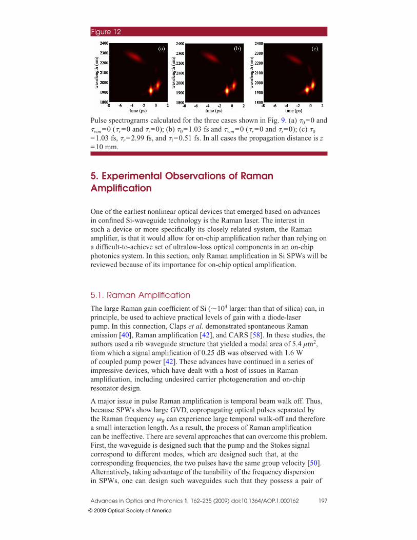
5A
Oisaapr
5
Tppeafoiar
AbtacFccAi
P ==
A
©
. Experimental Observations of Ramanmplification
ne of the earliest nonlinear optical devices that emerged based on advancesn confined Si-waveguide technology is the Raman laser. The interest inuch a device or more specifically its closely related system, the Ramanmplifier, is that it would allow for on-chip amplification rather than relying ondifficult-to-achieve set of ultralow-loss optical components in an on-chiphotonics system. In this section, only Raman amplification in Si SPWs will beeviewed because of its importance for on-chip optical amplification.
.1. Raman Amplification
he large Raman gain coefficient of Si (�104 larger than that of silica) can, inrinciple, be used to achieve practical levels of gain with a diode-laserump. In this connection, Claps et al. demonstrated spontaneous Ramanmission [40], Raman amplification [42], and CARS [58]. In these studies, theuthors used a rib waveguide structure that yielded a modal area of 5.4 µm2,rom which a signal amplification of 0.25 dB was observed with 1.6 Wf coupled pump power [42]. These advances have continued in a series ofmpressive devices, which have dealt with a host of issues in Ramanmplification, including undesired carrier photogeneration and on-chipesonator design.
major issue in pulse Raman amplification is temporal beam walk off. Thus,ecause SPWs show large GVD, copropagating optical pulses separated byhe Raman frequency �R can experience large temporal walk-off and thereforesmall interaction length. As a result, the process of Raman amplification
an be ineffective. There are several approaches that can overcome this problem.irst, the waveguide is designed such that the pump and the Stokes signalorrespond to different modes, which are designed such that, at theorresponding frequencies, the two pulses have the same group velocity [50].lternatively, taking advantage of the tunability of the frequency dispersion
Figure 12
ulse spectrograms calculated for the three cases shown in Fig. 9. (a) 0=0 and
wm=0 ( r=0 and i=0); (b) 0=1.03 fs and wm=0 ( r=0 and i=0); (c) 0
1.03 fs, r=2.99 fs, and i=0.51 fs. In all cases the propagation distance is z10 mm.
n SPWs, one can design such waveguides such that they possess a pair of
dvances in Optics and Photonics 1, 162–235 (2009) doi:10.1364/AOP.1.000162 197
2009 Optical Society of America

wt
BcsTswcn[tpwStfT=pga
Ts[
Owc
A
©
avelengths situated on either side of a ZGVD point and, again separated byhe Raman frequency �R, such they have the same group velocity [137].
ecause the Raman effect is a nonlinear optical process, tighter opticalonfinement can lead to an increase in the efficiency of the process, whichuggests that Si wires would make an effective gain medium. An example of aE-polarized Raman amplifier using SPW made use of a pumping setupimilar to Fig. 1. In the experiments using this device, the SPW was pumpedith a continuous wave (CW) source at 1435 nm and injected with a
ounterpropagating signal beam centered at 1550 nm with a bandwidth of 40m. The SPW had a propagation loss of �3.6±0.1 dB/cm at 1550 nm84] with input and output coupling losses of �1.5–2 dB/coupler. In this casehe input pump power was 20.5 mW with an on–off gain of 0.4 dB. Theower dependence of the gain exhibited a gain maximum at �=1550.7 nm,hich corresponded to the predicted �=15.6 THz �521 cm−1� Raman shift ini [40]. The measured on–off gain versus input pump power, i.e., that entering
he waveguide, is shown in Fig. 13. The maximum gain was G�0.7 dB (15%)or a pump power of PR�29 mW and for a waveguide length of L=4.2 mm.he Raman amplifier figure of merit (FOM), which is defined as FOMG / �PRL�=57.47 dB/cm/W, was substantial compared with earlyulsed-format devices. Furthermore, this increase in the FOM showed that theain scales approximately inversely with modal area. The data in Fig. 13re approximately linear with a slope of 0.029 dB/mW.
he data gathered in this measurement can be compared with the results of aimple numerical solution of the stimulated Raman differential rate equations101], viz.
dPp�z�
dz= −
�p
�R
gRPp�z�PR�z� − �Pp�z� −�TPA
Aeff
Pp2�z� ,
Figure 13
n–off gain versus input pump power. The maximum gain is 0.7 dB (17%)ith a pump power of �29 mW. A linear fit with a slope of 0.029 dB/mW
orresponds to an SRS coefficient gR�29 cm/GW. From [43].
dvances in Optics and Photonics 1, 162–235 (2009) doi:10.1364/AOP.1.000162 198
2009 Optical Society of America

wtw=RaPT(ctStSbll
5
Onapsba
ThtuwslaeomUrnorapRiut
A
©
dPR�z�
dz= �PR�z� −
gR − �TPA
Aeff
Pp�z�PR�z� , �39�
here PP and PR are the pump and signal powers, respectively, �P and �R arehe pump and signal frequencies, �=3.6 dB/cm is the propagation loss of theaveguide, �TPA=0.44 cm/GW is the assumed TPA coefficient [42], Aeff
0.059 µm2 is the effective modal area, and gR=29 cm/GW is the stimulatedaman scattering coefficient. The solution to these equations takes intoccount the effective pump power that is due to the finite pump bandwidth, i.e.,
eff=Pp / �1+�p /�R�, where �P=160 GHz and �R=105 GHz [42,113].he effect of pump depletion, i.e., the coupling term in the first equation in Eqs.
39), was also accounted for in the calculation and was negligible in thisase [43]. The calculated data, shown as a dashed line in Fig. 13, have a slopehat matched the experimental data to within ±10%. The on–off gain andRS coefficient found in this experiment agree well with the results of [42]. In
his case the use of a deeply scaled down waveguide cross section of anPW meant not only that the power is enhanced because of modal confinementut also that the transit time of the carriers is reduced compared with that inarger waveguides. In the experiment of [43], the effective recombinationifetime was found to have an upper bound of 0.77 ns.
.2. Removal of Photogenerated Carriers
ne of the major issues in Raman amplification as well as in many of theonlinear optical devices discussed below is the generation of carriers by TPA,s these carriers can generate active absorption in the waveguide. Thisrocess becomes a particular problem as one shifts the pump wavelength tohorter wavelengths from, say, �1700 nm. Free carriers can be eliminated eithery recombination, as mentioned above, or by carrier sweep out throughpplication of a transverse voltage.
he most obvious approach to reducing FCA is to use a pulsed Raman source,aving a pulse repetition rate much less than that of the recombinationime. In fact, many of the initial Raman amplification and Raman laser sourcessed this straightforward approach [40,42,44–48,51,52,54,123], whichhile of limited applicability for a practical high-data rate device, is useful to
tudy the physics issues in a Raman amplifier or laser, including nonlineaross mechanisms and carrier-lifetime effects. A second approach uses variouspproaches to decrease the recombination in the waveguide region. Anxcellent example is the use of He implantation to shorten lifetime [138]. Inne experiment using this approach, He implantation with a 1012 cm−2 dose wasade for a relatively large Si waveguide of cross section of 4.1 µm�2.8 µm.se of the He implantation formed recombination centers in the Si to
educe the free-carrier density and thus its power loss. As a result, theonlinearity, as judged by SPM measurements, was increased. Recombinationf carriers can also be enhanced by reducing the cross section of the gainegion, since that allows more rapid recombination at the walls [124]. Thispproach is applicable to amplification in Si wires, which have the smallestossible waveguide cross section. In fact, this approach led to the first CWaman devices, including that used in the CW amplifier example given above;
t also plays an important role in reducing FCA in high-repetition-rateltrafast lasers as long as the repetition rate is less than the recombination
ime. [47].dvances in Optics and Photonics 1, 162–235 (2009) doi:10.1364/AOP.1.000162 199
2009 Optical Society of America

CtidrTcw1o
AmtFrawar
6
Tte��coeda
6
Oo(dottti�rpise
A
©
arrier sweep out is the second approach for reducing carrier absorption; thisopic has been the subject of numerous studies and has led to severalngenious device designs. For example, work in [139] showed that optical loss,ue to FCA that was induced by TPA, may be significantly reduced byeverse biasing a p-i-n diode formed on the side regions on a rib waveguide.his biasing enabled the researchers to obtain higher CW Raman gain than whenarriers were not removed, i.e., with no applied voltage, from the SOIaveguide, which was a 4.8 cm long waveguide with an effective core area of.6 µm2. With carrier sweep out, the amplifier had a net CW Raman gainf 3 dB with an internal pump power of 700 mW.
third approach has recently been proposed in mitigating the FCA effect byaking use of a cladding-pumped geometry [140]. This configuration reduces
he overlap of the pump beam with the Si core, thus weakening the effect ofCA. Consequently, the length of the amplifier may be made much longer,esulting in a higher total gain not possible in a direct core-pumped CW Ramanmplifier. For example, numerical calculations assuming pump and Stokesavelengths of 1220 and 1303 nm, respectively, show that total gains as high
s 18 and 34 dB may be achieved with pump powers of 300 mW and 1 W,espectively, for Si-wire dimensions of h�w=270 nm�350 nm.
. Observations of Optical Nonlinearities in Si Wires
he optical properties of Si wires are such that it is relatively easy to drivehe wires into a strongly nonlinear regime with modest input power. As anxample, at pump peak powers of �1 W, corresponding to �P0
22.5 cm−1 in a 220 nm�450 nm cross-section waveguide, intensities of1GW/cm2 can be attained inside the waveguide. These intensities, in
onjunction the extremely large ��3� of Si, are sufficient to readily observe allf the key nonlinear phenomena in optical fiber. In this section, thexperimental observation of each of the principal nonlinear optical effects areiscussed, including optical limiting, SPM and XPM, soliton generation,nd MI.
.1. Optical Limiting
ptical transmission limiting, or simply “optical limiting,” is a readilybservable nonlinear response in tightly confined SPWs. For ultrashortfemtosecond) pulses, the origin of the phenomena is dominantly TPA, althoughepending on the pulse length other effects such as free-carrier generationr SPM can influence the effect to a greater or lesser degree. An example ofypical data is shown in Fig. 14. In this figure, two examples [72,73] are choseno illustrate limiting in different but important temporal regimes. Specifically,he graph shows results corresponding to a train of 1.8 ps and 200 fs pulses,njected into waveguides of nearly identical cross sections, i.e., 220 nm
450 nm, so as to have the same time-averaged carrier lifetime. The waveguideesponse is different for these two pulse regimes; Fig. 14(a) showsicosecond-pulse pumping, a regime where GVD is minimal, so that the SPMs the main optical effect that affects the pulse propagation, and Fig. 14(b)hows ultrashort ��200 fs�-pulse pumping, where GVD becomes significant
nough such that, in conjunction with the SPM, it severely distorts the temporaldvances in Optics and Photonics 1, 162–235 (2009) doi:10.1364/AOP.1.000162 200
2009 Optical Society of America

acisapip
FptsswtpsoTtdlmEl
Tiiiidl�tp
Da
A
©
nd spectral pulse profile as is shown in the next subsection. The maximumoupled-input peak powers for both cases are a few watts. However, for the casen Fig. 14(b), the simulations showed that the TOD effects are also sufficientlytrong to significantly distort the output-pulse spectrum; thus in this casebetter measure for the optical power carried by the pulse train is the averageower. Consequently, Fig. 14(a) displays the output peak power versus thenput peak power, while Fig. 14(b) displays average power versus input peakower.
or both cases, the output power scales linearly with the input power for inputeak powers below �50 mW and saturates above this input power. Althoughhe powers required for achieving the onset of saturation are similar, theaturation mechanism for each case is different. For the case of the longer pulses,aturation occurs due to absorption from free carriers generated by TPA,hile for the short pulses, saturation is due predominantly to direct optical loss
hrough the TPA process itself. The onset of saturation in both cases isredicted accurately by the numerical solution of Eqs. (23) and (15), which ishown by the curves in each panel. In particular, this simulation predictsptical peak powers in the range �50–100 mW, near the onset of saturation.he free-carrier-induced loss for the 1.8 ps case is approximately eight
imes that of the 200 fs case. In other words, owing to the difference in pulseuration for the two cases, the relative pulse energy is approximately 10:1 for theong pulse as compared with the short pulse; thus the longer pulse yieldsore carriers than the shorter pulse by an order of magnitude, as seen fromq. (23), and therefore the corresponding free-carrier-induced losses are also
arger.
he mechanism for the saturation behavior in each of the two cases wasnvestigated in detail by numerically solving Eqs. (23) and (15). The solid curvesn Fig. 14 denote the theoretical predictions for both cases. The calculationn this case takes into account the total dispersion and other linear effects,ncluding FCA. For the case of the short-pulse pumping, the TPA processominates and causes optical limiting at high peak powers. In contrast, for thisow power, the photogenerated free-carrier-density is only N�3
1015 cm−3, which is comparable with the unexcited carrier density. Hence,he effect of losses from these TPA-generated carriers for the short-pulse
Figure 14
ependence of output power on coupled input power for (a) 1.8 ps (from [72])nd (b) 200 fs pulses (from [73]). Experiment, squares; simulations, curves.
umping case is negligible. In fact, in this case, the numerical simulations were
dvances in Optics and Photonics 1, 162–235 (2009) doi:10.1364/AOP.1.000162 201
2009 Optical Society of America

ddnpssfmdfsl
6
Iso(cawasfcsT
FirocAAc
Ffwepwobfowbdgr
A
©
one both in the presence and the absence of FCA, and, as expected, noifference was observed between these two cases as shown in Fig. 14(b). Ourumerical calculations also showed that choosing sech- or Gaussian-shapedulses leads to approximately the same results, as long as the FWHM is kept theame. For the case of picosecond pumping, shown in Fig. 14(a), near theaturation threshold power value of, say, �60 mW, the optical power leads to aree-carrier density of N�2�1017 cm−3, which is about 2 orders ofagnitude greater than the carrier density in the unexcited waveguide (p
oped, N�1�1015 cm−3). Finally, note that the interpulse carrier accumulationrom multiple pulses in either of the examples is negligible in our experiments,ince the temporal separation between adjacent pulses is significantlyonger than the carrier lifetime.
.2. Self-Phase Modulation and Third-Order Dispersion
n addition to optical limiting behavior, optical pulses propagating in a SPWhow increasing spectral modulation, as the pump power is increased. The originf this process, which is well known in fiber optics, is shown clearly by Eq.29) above (with the XPM term set to zero); the nonlinear response of the SPWauses the phase to shift in time during the pulse propagation, thus inducingfrequency shift. This effect is seen clearly in more exact numerical simulations,hich show that as the input power is increased, the pulse spectrum broadens
nd then develops a multiple-peak structure. This behavior, which is aignature of the SPM, is the result of the phase interference between the pulserequency components with a time-dependent SPM-induced frequencyhirp. These simulations also clearly illustrate that the Si-wire SPM can betrongly influenced by the optical properties of the medium, including TPA,PA-induced free carriers, and, for �1 ps pulses, TOD.
or typical pulsed-laser telecommunication sources, the short carrier lifetimen SPW does not allow interpulse carrier accumulation. However, the laserepetition rate can play an important role if the lifetime of the carriers is longerr comparable to the interpulse temporal separation, since in this casearrier accumulation may become a source of phase shift (as well as loss).ccumulation is particularly important in large-cross-section waveguides, i.e.,
01 µm2, and if no applied voltage is present to sweep out photogeneratedarriers.
igure 15 illustrates the clear spectral broadening of picosecond andemtosecond pulses upon propagation in SPWs with approximately the sameaveguide dimensions. In addition to broadening, the spectra in Fig. 15(b)
xhibit strong spectral modulation and more pronounced asymmetry of the pulserofile than do the spectra in Fig 15(a). Both of these properties increaseith input power. Spectral asymmetry, in general, may result from FCA, TOD,r the initial input-pulse asymmetry. In optical fibers, SPM-induced spectralroadening of picosecond pulses is normally symmetric around the centerrequency [101]. Similarly, only minimal asymmetry is observed for propagationf such pulses in SPWs [72]. This situation is different for much larger Siaveguides, in which carrier lifetimes are longer and the resulting absorptiony photogenerated FCA can cause spectral asymmetry [68]. However, asiscussed above for the case of optical limiting experiments, while free-carriereneration can be a significant for picosecond or longer pulses, it is greatly
educed for femtosecond pulses because of the low pulse energy typically used.dvances in Optics and Photonics 1, 162–235 (2009) doi:10.1364/AOP.1.000162 202
2009 Optical Society of America

Icl
TtcwsarCase
Sff
Cp(pDs
A
©
n fact, in the case of the �200 fs data in Fig. 15(b), simulations using theoupled-mode equations have shown clearly that TOD is the dominant effecteading to the spectral asymmetry seen in this figure.
he changes in the spectral features in Fig. 15(b) are to first order a result ofhe spectral modulation induced by SPM. The high nonlinearity of Si and its tightonfinement in Si wires means that this modulation can be seen in SPWsith lower input power and many orders of magnitude shorter distance than in
tandard optical fibers. Of course, as mentioned above, effects such TPAnd its resulting free-carrier generation further modify the otherwise pure SPMesponse of the Si wire—as does the influence of TOD in shorter pulses.learly, also, the spectral shape of the output pulse presents additional features,s compared with the input spectra. These changes can be accuratelyimulated with the coupled-wave equations. For example, Fig. 16 shows thexperimental and simulation results obtained by using a sech pulse shape for
Figure 15
elf-phase modulation observed experimentally using picosecond andemtosecond pulses. (a) 1.8 ps pulses (figure from [72]) (b) 200 fs pulses (datarom [73]).
Figure 16
omparison of simulation with experimental measurements of pulsesropagating in a SPW waveguide with �P0=56.3 cm−1. Left, measured spectrabrown). Right, simulation using sech input pulse (red). Blue curves on bothanels correspond to �P0=1.1 cm−1 (with sech input pulse for simulation).ashed line, OSA noise floor. The numbers illustrate features of the output
pectrum common to experiment and simulation. From [73].
dvances in Optics and Photonics 1, 162–235 (2009) doi:10.1364/AOP.1.000162 203
2009 Optical Society of America

tpspa
6
IsoSdiostwmp�tiDS
Apeeeseampsstsplb
Tcibtsada
A
©
he 200 fs pulse; the numbers 1–8 indicate a series of smaller features oreaks. The agreement between data and simulations is excellent if a sech pulsehape is used. Simulation of the same data set using Gaussian-shaped inputulses gives less spectral features, but a more realistic imbalance between the leftnd right peaks.
.3. Soliton Generation
n a nonlinear optical medium the generation of solitons is possible. Theseolitary optical waves are stationary states of propagation and are formed by anptical increase in the nonlinear index by a high-intensity propagating wave.oliton formation requires that the guided-wave medium exhibit anomalousispersion. They are potentially important as a communication format and are,n any case, a component essential to the full understanding of the nonlinearptics of a medium. Several experiments and optical simulation have shown thatoliton radiation and its effects can be readily seen in SPWs. For example,he work of Hsieh et al. [73] matched the observation of soliton effects in SPWsith the results from numerical simulations. Recently, in a relatedeasurement, Zhang et al. also observed related effects regarding soliton
ropagation in larger Si rib waveguides having dimensions of 400 nm860 nm and an etching depth of 300 nm [141]. In addition, in a recent
heoretical study, the role of fission of higher-order solitons in Si waveguidesn driving supercontinuum radiation [142] was discussed. More recently,ing et al. reported measurements and simulations of soliton propagation fromPWs having three to four dispersion lengths [143].
s in optical fibers, radiation from solitons may be generated during theropagation of soliton pulses through the influence of higher-order perturbativeffects, particularly TOD [126–129]. However, in the case of Si wires theffective nonlinear coefficient is �105 larger than that in fibers, and thus solitonffects are seen in wires only millimeters in length. This radiation may beeen as a feature in the output spectrum of a propagating pulse in a SPW,xhibiting anomalous dispersion. For example, in addition to the featuresttributable to SPM in Fig. 16, an additional spectral feature is observed, whichay be attributable to soliton radiation. The evolution of the spectra with
ower is shown in Fig. 17, which displays both experimental and numericalimulation results. This figure shows that as the input power increases, apectral feature develops near 1590 nm for �P0=45 cm−1 (brown curve); noticehat the peak is significantly shifted from the main SPM features. Theoliton number for the conditions in Fig. 16 is Nsoliton=6.6, and thus pulseropagation is clearly in the soliton regime. Finally and characteristically, theocation of this peak remains constant over a large range of powers, aehavior not seen in SPM features.
he location of this peak can also be used to determine the waveguide TODoefficient—a technique similar to that first used to measure �3 of optical fibersn the vicinity of the zero group-delay dispersion point [144]. In particular,y using the position of this spectral peak we can infer the value of �3 by usinghe relation �3=3��2�T0 /�r, where �r is the normalized angular frequencyeparation between the center frequency and the soliton feature [126–129] (seelso Subsection 4.6). Note that this relation does not account for theependence of �r on dispersion coefficients beyond the third order, as well as
ny power dependence of the propagation constant; however these effectsdvances in Optics and Photonics 1, 162–235 (2009) doi:10.1364/AOP.1.000162 204
2009 Optical Society of America

apuocp
6
Stecodcfiib
Ftwvhp1XcXidpa
C1e1
A
©
re small and are commonly neglected. In addition, while this relation uses theulse width T0 in the expression for �3, a more rigorous approach can besed in the case of multiple soliton generation. Thus, in this case, instead of T0
ne uses the temporal width of the corresponding emitted soliton. Theentral point, however, is that this approach can be used to probe waveguideroperties such as TOD.
.4. Cross-Phase Modulation
PM alters the phase of an optical pulse as it propagates through the wire; it isherefore crucial to consider this effect when the optical peak power is largenough that the pulse propagation is in the nonlinear regime. In addition, in theases where a second pulse is present, it is important to include the alterationf the phase of a pulse at one wavelength by a second, copropagating pulse, at aifferent wavelength, i.e., XPM. XPM is described by the generaloupled-mode theory presented in the set of equations (27). Unlike in opticalbers, in Si wires the XPM process can be altered by the strong dispersion
n a SPW and by the fact that TPA is present. These points will be discussedelow.
igure 18 illustrates the effect of XPM of a weak probe pulse by a pump pulse;hese two pulses have different wavelengths and copropagate in the sameaveguide [77]. The pump power corresponds to �psPp=10.4 cm−1, for severalalues of the pump–probe delay time. The pump and the probe or signalave center wavelengths at �p=1527 nm and �s=1590 nm, respectively. Theulse width and bandwidth of the resulting pulses are approximately 200 fs and5 nm, respectively. The figure shows the dependence of the strength ofPM on the temporal overlap between the two pulses. These results illustrate
learly spectral variations in the probe spectrum, which can be induced byPM. It was shown in [77] that as the nonlinearity-pump-power product
ncreases, a larger number of oscillations are induced in the waveform, a resultue to the increasing index change at higher pump powers. Similarly, as theump overlap increases, the modulation of the signal by the pump as increases
Figure 17
hange in output spectra due to SPM for different excitation levels �P0=1.1,1.3, 33.8, 45.0 cm−1 (bottom to top) spectra for both (a) theory and (b)xperiment. Note also the evolution of soliton radiation (dashed line) at590 nm.
s shown in Fig. 18.
dvances in Optics and Photonics 1, 162–235 (2009) doi:10.1364/AOP.1.000162 205
2009 Optical Society of America

Owtpi[tqispG re
Dp
Efc
A
©
ne approach to examining the physics of XPM is to examine the shift inavelength of a signal pulse as the delay between pump and probe pulse, prior
o injection into a waveguide, is varied. Since this delay controls the temporalrofile of the refractive index change induced by the copropagating pump pulse,t maps out the wavelength change in the carrier frequency or wavelength145] with power or index change. This shift can be described conveniently byhe centroid wavelength of the spectrum, �c=�P���� d� /�P��� d�. Theuantity �c shifts as the temporal delay between the pump and the probe pulsess varied. Figure 19 illustrates the shift in �c, that is, the nonlinear frequencyhift of the centroid or mean wavelength, induced by changes in the pump–robe delay. This frequency shift was given above in Eq. (33) for the case ofaussian pulses, ��s�−�exp�−� − d+��2�−exp�−� − d�2��, where, again,
, d, and �, are normalized time, normalized time delay, and temporal walk-off,espectively. For the waveguide length and pulse widths used in ourxperiments, the normalized temporal walk-off is �=L /Tp=4.78 [77]. At
Figure 18
emonstration of XPM in SPWs. Dependence of probe spectrum on pumpower and pump–probe delay.
Figure 19
xperimental (red) and numerical simulation (blue) of the shift in centerrequency due to XPM with the time delay of the pump and probe pulse. Theenter wavelength of the probe is �1590 nm.
dvances in Optics and Photonics 1, 162–235 (2009) doi:10.1364/AOP.1.000162 206
2009 Optical Society of America

lp=tHfabwompatbdtsant
FcldaTfa
WmuatdrvbtptemprttdF
T�
A
©
arge absolute values of d, no wavelength shift is observed because the twoulses do not overlap in the waveguide. On the other hand, if either d=0 or d
�, XPM interaction induces a large nonlinear wavelength shift, which forhe data in Fig. 19 is 1 nm but is negative for d=0 and positive for d=�.owever, in the vicinity of d=� /2, no shift is observed, since two shifts
or the front and the rear of the waveguide effectively cancel each other. Thesymmetry in the nonlinear shift of the probe centroid wavelength is explainedy the presence of a small linear loss in the waveguide. Thus in the case inhich d=0 the pump–probe interaction takes place mostly near the input facetf the waveguide, whereas when d=� the pump interacts with the probeostly near the output of the SPW, i.e., after the pump has lost part of its optical
ower because of intrinsic and TPA losses. In addition, the pulse width islso changed asymmetrically. Specifically, the peak near d=0 is narrower thanhe one near d=�, a behavior that is attributable to the slight temporalroadening of both the pump and the probe pulses because of frequencyispersion. Figure 19 also shows a fit to experimental results obtained by usinghe coupled-mode theory. The model accurately predicts the variation ofhift with delay, as well as other more detailed features of the shift. For example,lthough the temporal broadening of the signal pulse with delay is small, theumerical simulation shown in Fig. 19 shows a small difference in the width ofhe two lobes.
inally, because of the large effective nonlinear coefficient for Si and the highonfinement of SPW, the absolute value for the frequency shift can bearge—even with a relatively modest pump. For example, Dekker et al.emonstrated XPM-induced wavelength shifts of as much as 10 nm, whichre comparable with the spectral width of the input probe pulses [76].hese results suggest that a XPM-induced frequency shift could be employed
or an ultrafast all-optical switch, which can be used to switch off pulsess short as a few hundred femtoseconds.
ith regard to optical switching, the nonlinear switching properties of devicesay be described in terms of the FOM, where FOM=n2 /�TPA�, which is
sed to quantify the nonlinear phase shift achieved over an effectivebsorption-limited length [146]. The FOM value is relatively independent ofhe dimensions of the waveguide; however, the operational value of the FOM isevice specific; i.e., it depends on the switching mechanism. Thus theequired nonlinear phase shift varies from � to 4�, corresponding to FOMalues of 0.5–2. For bulk Si, FOM=0.37, which suggests that Si wires may note ideal for certain forms of nonlinear optical switching components. Forhe Si wires, n2 and �TPA are strongly enhanced by the waveguide confinementroperties. But because the enhancement to n2 and �TPA are comparable,he FOM does not change significantly from the bulk values. However, thextremely low pulse energy required for Si-wire devices is itself interesting anday justify utilizing the low FOM value of Si despite its associated
erformance penalty. Further, since in the case of XPM-based switches, theequired FOM is decreased to half of the value corresponding to the SPM case,hese switches may be even more attractive [77]. As a final point, because ofhe pronounced wavelength dependence of both n2 and �TPA, the FOM for SPWevices will increase substantially with wavelength until at �2200 nm theOM is �4.4 [39].
he use of XPM [74] for switching has been demonstrated in waveguides of
2 µm in cross section, thus larger than typical Si wires. This work used advances in Optics and Photonics 1, 162–235 (2009) doi:10.1364/AOP.1.000162 207
2009 Optical Society of America

M�sTpidltwtts
6
Ambardfaneg
FgwFSIw
Mcsmt(awitfbTm
It
A
©
ach–Zehnder interferometric device with the two wavelengths separated by25 nm. In this experiment, switching was governed at picosecond and
horter times by Kerr nonlinearities and at longer times by index change due toPA-induced free-carrier loss. The Kerr nonlinearity was important forowers up to the 40 W pulse peak power. However, as the peak power levelncreased, free-carrier effects became important. Such effects includedistortion in the switching transient. Switching speeds due to free carriers wereimited by the �1–10 µs recombination times, which are greater than aypical picosecond switch pulse. These carriers accumulate from pulse to pulse,hen the recombination time is longer than the interpulse time scale. Despite
he importance of free-carrier generation, it was found that it was possibleo attain a Kerr phase shift of 180° at power levels lower than those, for whichubstantial free carrier generation occurs.
.5. Parametric Processes: Frequency Mixing
final class of basic nonlinear processes to review is that of parametricixing. This process is an important optical functionality, since it includes
asic operations such as frequency upconversion and downconversionnd wideband amplification. It is also a process that for efficient operationequires phase matching, which can be achieved via control of the waveguideispersive properties, and a strong Kerr nonlinearity. As a model exampleor this discussion, consider wavelength conversion by means of techniques suchs FWM. This process is related to several other important third-orderonlinear optical processes such as CARS, parametric amplification,lectric-field-induced second-harmonic generation, and third-harmoniceneration.
WM using Si photonics has been demonstrated and explored by manyroups. For example, Fukuda et al. showed the possibility of FWM in Siaveguides for frequency conversion [61]. In this experiment, conventionalWM was used wherein two input beams at frequencies �1 and �2 interact in thei waveguide to generate new output frequencies at 2�1−�2 and 2�2−�1.n this experiment there was little effort to engineer dispersion, and thus mixingas limited in tunable spectral bandwidth and in efficiency.
ore complex FWM schemes can be used, which are less demanding in theontrol over Si-wire dispersion, that is, for a case in which the waveguide crossections are fixed by considerations other than for the FWM process. Thus aore general FWM process is shown in Fig. 5(e) (first two panels), in which
hree beams of different wavelengths, for example, two pump laser beamsp1 and p2) and a signal laser beam �s�, interact in a ��3� medium to producen output �o� idler beam. For the same pump and signal wavelengths, twoavelength-mixing processes are possible as seen in Fig. 5(e); hence two output
dler beams are generated. The advantage of this more general scheme overhe conventional FWM process is that the more general scheme allowsor operation of the pump (control) laser wavelengths over a wider spectralandwidth while keeping the phase mismatch minimal for efficient conversion.his scheme can be an important consideration in a strongly dispersiveedium, such as a Si waveguide.
n addition, in certain FWM schemes, resonances may play a role in enhancing
he nonlinear optical susceptibility, as in the case of CARS. Further, in thisdvances in Optics and Photonics 1, 162–235 (2009) doi:10.1364/AOP.1.000162 208
2009 Optical Society of America

cFt(pacuiRrudwcpm
Itttpowrerf
FadRicc
TTs
wriid
A
©
ase the relevant third-order susceptibility, ��3�, is that for Raman interaction.igure 5(c) illustrates the energy diagram for the CARS process wherein
he photon energy difference between the pump and signal matches the phononRaman) energy. In such a process, two photons derived from the sameump laser �p� interact with the (Stokes) signal photon in the medium to producen output photon whose angular frequency is given by �CARS=2�p−�s. Byomparison with the electronic ��3� processes just described, CARS is moreseful for larger waveguide experiments because of the stronger dispersionn SPWs. In addition, the electronic susceptibility ��3� is much weaker than theaman susceptibility, �R
�3� by �1/44 [27] owing to the presence of theesonant terms in the expression for the Raman susceptibility. In fact, FWMsing CARS was one of the earlier wavelength conversion techniquesemonstrated. In the initial demonstration of CARS, wavelength conversionas achieved in a 5.4 µm2 cross-section Si waveguide [58]. Wavelength
onversion was achieved from �s=1542 nm to �CARS=1329 nm by using aump laser at �p=1427 nm with a −50 dB efficiency corresponding to a phaseismatch of ���=27 cm−1.
n the case of a SPW, the applicability of CARS has some limitations despitehe attraction of the tighter optical confinement afforded by such a small,ightly confined waveguide. However, in fact, waveguide dispersion dominateshe modal dispersion, thus making it difficult to achieve efficienthase-matched conversion. For example, a typical SPW has a phase mismatchf ����600 cm−1 for the CARS process! In addition, for a fixed signalavelength, �s, the CARS process is not tunable, since the resonance condition
equires that �p−�s=�R. Finally, despite the fact that the nonresonantlectronic susceptibility ��3� is smaller than the Raman susceptibility atesonance, the decreased cross-sectional area of the waveguide compensatesor the weaker electronic ��3�.
requency mixing has been demonstrated in SPW waveguides by means of thebove nonresonant, nondegenerate FWM scheme by using low-power, CWiode-laser sources, corresponding to the first two panels of Fig. 5(e) [60].elatively efficient mixing was observed despite the large phase mismatch
mposed by strong waveguide dispersion. The experimental results, includingonversion efficiency, agree well with theoretical calculations based onoupled-mode theory. Frequency tuning of the idler from �20 GHz to100 GHz was demonstrated [60].
he physics of this process is shown clearly by this coupled-wave treatment.he energy conservation and phase-matching conditions of this conversioncheme are
�o± = �s ± ��p1 − �p2� ,
� = �o± − ��s ± ��p1 − �p2�� , �40�
here p1, p2, s, and o correspond to the two pumps, signal, and output fields,espectively, and �i=neff��i��i /c, where neff is the effective refractivendex. For the (+) configuration in Eq. (40), the propagation properties and thenterchange of energy between these four fields within the waveguide are
escribed by four nonlinear, coupled-mode differential equations [101]:dvances in Optics and Photonics 1, 162–235 (2009) doi:10.1364/AOP.1.000162 209
2009 Optical Society of America

wr�SsfXFtc
(s=a
A
©
dEp1
dz+
1
2�p1Ep1 = i�p1��Ep1�2 + 2�Ep2�2 + 2�Es�2 + 2�Eo�2�Ep1
+ 2i�p1Es*Ep2Eo exp�i�z� ,
dEp2
dz+
1
2�p2Ep2 = i�p2��Ep2�2 + 2�Ep1�2 + 2�Es�2 + 2�Eo�2�Ep2
+ 2i�p2Ep1EsEo* exp�− i�z� ,
dEs
dz+
1
2�sEs = i�s��Es�2 + 2�Ep2�2 + 2�Ep1�2 + 2�Eo�2�Es
+ 2i�sEp1* Ep2Eo exp�i�z� ,
dEo
dz+
1
2�oEo = i�o��Eo�2 + 2�Ep1�2 + 2�Es�2 + 2�Ep2�2�Eo + 2i�oEp1EsEp2
*
�exp�− i�z� , �41�
here �i and �i are the propagation loss and the nonlinear coefficient,espectively, corresponding to wavelength �i. The parameter n2=4.5
10−18 m2/W [108], and Aeff=0.06 µm2 is the effective modal area [41].ince the nonlinear coefficient �i� �Aeff�−1, the FWM conversion efficiencyhould be enhanced as the cross-sectional area is decreased. The first, second toourth, and fifth terms on the right-hand side of Eqs. (41) are due to SPM,PM, and FWM interactions, respectively. The effects of TPA and TPA-inducedCA are neglected because of the low powers used in this experiment. For
he case of the (+) configuration of Eqs. (40), the idler wavelength ��o+� and theorresponding phase mismatch, �, are shown in Fig. 20(a). Solving Eqs.
Figure 20
a) Converted wavelength and phase mismatch versus pump–wavelengtheparation. (b) Conversion efficiency versus phase mismatch for �0.148 nm at two possible propagation losses of �=3.5 dB/cm (solid curve)nd 0.1 dB/cm (dashed-dotted curve). From [60].
dvances in Optics and Photonics 1, 162–235 (2009) doi:10.1364/AOP.1.000162 210
2009 Optical Society of America

(ps=es
I[tlpKc
6
AptttivntTd
wtetmtt
wa
Tdac
w
A
©
41) gives the conversion efficiency shown in Fig. 20(b). As an example, forump wavelengths of �p1=1435 nm and �p2=�p1+�, where �=0.148 nm, aignal wavelength of �s=1550.5 nm, and the output wavelength of �o+
1550.3 nm, the phase mismatch is ���=0.6 cm−1 and the conversionfficiency is −20 dB. The corresponding analysis for the (−) configuration yieldsimilar results.
n addition, ultrabroadband parametric generation and wavelength conversion66] have been examined for the case in which the pump beam is close tohe zero dispersion wavelength of a SOI waveguide. Under strongong-pulse-width pumping, free-carrier effects were shown to affect therocess; but with short pulses, i.e., �1 ns, FWM with a pulsed pump, the strongerr effect allowed efficient parametric amplification and wavelength
onversion.
.6. Tunability of Four-Wave Mixing
s is shown in Fig. 20 above, the efficiency of the FWM is set by the degree ofhase matching among the interacting waves. We now consider the case ofhe FWM nonlinear optical interaction in Fig. 5(e) (third panel). To first order,he phase-matching condition involves ensuring that the wave vectors ofhe four interacting wave sum to zero, that is kL�0, where kL=2kp−ks−ki
s the linear phase mismatch and kp, ks, and ki are the propagation waveectors of the pump, signal, and idler beams, respectively. However, if anyonlinear changes in these wave vectors induced by SPM and XPM are included,he phase-matching condition must be modified to account for this variation.hus for the case of a single degenerate pump, the phase mismatch k for aetuning � between pump and signal is then
kNL = 2�Pp − kL �42�
here � is the effective nonlinearity, n2 is the nonlinear refractive index, � ishe wavelength of light, Aeff is the mode area, and Pp is the pump power. Thisxpression may be further corrected by including higher-order dispersion inhe expression for the linear phase matching. Only even phase-matching termsust be included, since odd orders cancel out because of symmetry. Thus
he first term that must be included is that of fourth-order dispersion; in this case,he linear phase mismatch is approximately
kL = − �2���2 −1
12�4���4, �43�
here the GVD coefficient �2 and the fourth-order dispersion coefficient �4
re calculated at the pump wavelength.
here are various definitions of conversion efficiency in use; one convenientefinition equates the efficiency to the ratio of the idler output to the signal input,ssuming conditions are such that there is essentially no TPA. Then the idleronversion efficiency �i=Pout,i /Pin,s is given by [147]
�i = ��Pp
gsinh�gL��2
, �44�
here
dvances in Optics and Photonics 1, 162–235 (2009) doi:10.1364/AOP.1.000162 211
2009 Optical Society of America

ipo
Dt
Nacfiee
Ub3bae1sg
Awdfwotipida
6
Alacbb
A
©
g = ��PpkL − �kL/2�2 �45�
s the parametric gain, Pout,i is the idler output power, Pin,s is the signal inputower, and L is the interaction length. Since the maximum efficiency �max,i
ccurs when k=0,
�max,i = sinh2��PpL�. �46�
efining the conversion bandwidth as that when �kL��� [101] and assuminghe small-gain limit 2�PpL��, the conversion bandwidth BWFWM is then
BWFWM �� 4�
�2L. �47�
otice that this bandwidth depends solely on the waveguide dispersion. Inddition, since for Si wires, � is 5–6 orders of magnitude larger than foronventional single-mode fibers, much shorter conversion lengths are possibleor comparable levels of efficiency [90,92,125]. These short lengths translatento higher conversion bandwidths for comparable values of �2 for Si wires. Forxample, interaction lengths for significant conversion of 1 cm are possibleven at modest input powers [100].
sing this FWM approach along with Si-wire waveguides, net on–off gain haseen demonstrated over a 28 nm bandwidth [64]. Thus, Si wires with a00 nm�550 nm cross section, designed to have anomalous dispersion over aroad range of frequencies, were used to demonstrate wavelength conversiont �1510 to 1590 nm, with a peak conversion efficiency of +5.2 dB. Asxpected, nonlinear TPA was found to be the major loss mechanism. A folded7 mm waveguide was implemented to offset the nonlinear absorption,ince this geometry allowed operating at lower pump power for a given level ofain. This 17 mm device had a 4.9 dB total on–off gain and 1.8 dB net gain.
n excellent example of using the dispersion engineering that is possible in Siires is contained in [100], which examines in detail the effect of waveguideispersion on the bandwidth of FWM and shows that very broad-bandwidthrequency conversion is possible with FWM. For example, by selecting aaveguide with low GVD, a demonstration was made of a conversion bandwidthf �150 nm at a conversion efficiency of −9.6 dB, as well as tuninghroughout the C band with a somewhat lower conversion bandwidth. Furthert was also shown that for pumping close to the ZGVD point, thehase-matching bandwidth was set by fourth-order dispersion [148,149], andn that case, by careful phase matching in the presence of this higher-orderispersion, the signal could be wavelength shifted from 1477 to 1672 nm withn efficiency of −12 dB.
.7. Free-Carrier Control
s in other nonlinear optical processes in Si-wires, TPA carrier generation canimit the efficiency and operating powers for FWM. However, by incorporatingp-i-n junction in a SOI waveguide, efficient FWM and, hence, wavelengthonversion, have been demonstrated [150]. In this case, carriers were swept outy the junction electric field in the junction-insulating region after reverse
iasing. The experiments used a Si-rib waveguide to achieve a wavelengthdvances in Optics and Photonics 1, 162–235 (2009) doi:10.1364/AOP.1.000162 212
2009 Optical Society of America

c4oawdrnilrtt
6
Mcioosvhng
AfmmoadrFsa
ToaG�c
FiwzlTte
A
©
onversion efficiency of −8.5 dB in an 8 cm long waveguide at pump intensity0 MW/cm2. With this high wavelength conversion efficiency, high-speedptical data transfer between C-band channels was demonstrated. In particular,10 Gb/s pseudo-random-bit-sequence data rate was converted to a secondavelength channel with minimal waveform distortion and with an open eyeiagram; in a subsequent study, it was demonstrated that the data transferate can be increased to 40 Gb/s [63]. The waveguides in this experiment wereot designed for phase matching; however, they could be folded for longernteraction length because of their low bend loss and carrier sweep out, thusowering the waveguide optical loss. Folding also, of course, allows greatlyeducing the on-chip footprint. Experiments have been done for other devicesypes to demonstrate the efficacy of carrier sweep out; see, for example,he discussion of this approach in Subsection 5.2..
.8. Modulation Instability
I represents the unstable evolution (exponential growth) of a CWopropagating in a nonlinear medium, an effect that is caused by the nonlinearnteraction between the propagating waves. In the context of nonlinearptics, MI has been studied extensively, particularly in regard to propagationf optical beams in optical fibers [151–156]. Since as a result of the MI certainpectral components grow exponentially, this nonlinear process can beiewed as providing gain at these particular frequencies, and therefore canave important applications. Note that in the case of a single beam, it isecessary for the medium to possess anomalous dispersion in order to have MIain.
s in FWM, MI enables SPWs to provide tunable optical gain at one or morerequencies. Recently, Panoiu et al. investigated theoretically this all-opticalodulation approach as a means to achieve strong optical gain in aillimeter-long SPW [137]. Specifically, their work demonstrated that two
ptical CW beams that copropagate in a SPW could generate a strong MI withinpropagation distance of just a few millimeters. The gain of this processepends on the power of the optical waves; thus it can be optically tuned, and iteaches its maximum value when both waves experience anomalous GVD.inally, note that, as a result of the MI, the optical waves develop deepubpicosecond modulation. This phenomenon can thus be used as the basis forn on-chip source of ultrashort optical pulses.
wo cases can be used to illustrate the optical physics for MI: case A, in whichne wave propagates in the normal GVD region, and the other experiencesnomalous GVD; and case B, in which both waves propagate in the anomalousVD region. The SPW for each case has dimensions h�w=220 nm360 nm, for which the ZGVD point is �0=1550 nm (this wavelength
orresponds to a second ZGVD point not shown in Fig. 3).
or both case A and case B, the dynamics of the two optical waves propagatingn the SPW are governed by system (27). The stability of these two opticalaves is studied first by finding the steady-state (CW) solutions, i.e.,
-independent solutions of this system of equations, and then by analyzing theinear dynamics of small perturbations of these solutions [101,151–156].hus, simple calculations show that, if we neglect the linear and nonlinear losses,
he MI gain spectrum defined by G���=2 Im������ is determined by the
quationdvances in Optics and Photonics 1, 162–235 (2009) doi:10.1364/AOP.1.000162 213
2009 Optical Society of America

wrs
NAwtIgtepTw1acad
AiIapofit
7
Mdst
Cd
A
©
��� − �/vg,p�2 − �p���� − �/vg,s�2 − �s� = ��4, �48�
here � and � are the frequency and the wave vector of the modulation,espectively, �=4�ps�sp�2p�2sPpPs, �p,s=�2p,s�
2��p,sPp,s+�2p,s�2 /4�, and the
ubscripts �p ,s� refer to the pump and the signal waves, respectively.
ow consider the MI gain in each of the two cases introduced above. In case, the pump beam propagates in the normal GVD region, �p=1625.3 nm,hereas in case B it experiences anomalous GVD at �p=1400 nm. In both cases
he signal beam propagates in the anomalous GVD region, at �s=1450 nm.n case A, the two wavelengths are selected so that the waves have the sameroup velocity, and thus there is no temporal walk-off, whereas in case Bhe walk-off parameter is = �1/vg,p−1/vg,s�=86.3 ps/m. Use of Eq. (48)nables the dependence of the gain spectra versus the pump power Pp (at a signalower Ps=200 mW in case A and Ps=40 mW in case B) to be determined.he results, presented in Fig. 21, show that in both cases the copropagatingaves experience strong MI, with a bandwidth of the gain spectrum of0 THz. For comparison, the Raman gain bandwidth of Si is much smaller, atpproximately 0.1 THz [43]. As discussed in Subsection 6.6, a potentiallyomparable gain bandwidth is expected in broadband FWM when the guide hasnomalous dispersion; in fact, gain bandwidths of a few terahertz have beenemonstrated experimentally for FWM [64].
lthough the powers Pp, Ps are smaller in case B, a larger MI gain is observedn this same case, namely, when both waves experience anomalous GVD.n addition, in both cases the MI gain is 102–103 times larger than the MI gainchievable in optical fibers, for similar values of the optical powers. Thisroperty arises from the fact that the � parameters, which determine the strengthf the MI gain, are much larger for SPWs as compared with those of opticalbers. In addition, the frequency corresponding to the maximum MI gain can be
uned by changing the power of the interacting waves.
. Applications of Nonlinearities in Si Nanowires
any applications of optical nonlinearities in Si nanowires have recently beenemonstrated. In this review, we illustrate these applications with a fewelected examples, which are representative of the range of possibilities forhis ultracompact guided-wave medium.
Figure 21
alculated MI gain spectra for the two case of (a) normal and (b) anomalousispersion described in the text.
dvances in Optics and Photonics 1, 162–235 (2009) doi:10.1364/AOP.1.000162 214
2009 Optical Society of America

7
SaWactf
PgptoitIt[o
Awcerdede
Amawtriww�sd
Few�shdbpc
A
©
.1. Continuum Generation
upercontinuum generation is a device functionality that has importantpplications in many areas of photonic integrated circuits [104], particularlyDM applications. In this application, for example, it is often beneficial to usesingle broadband laser source, selected by filtering specific wavelength
hannels, and then modulate these channels, instead of using a separate lasero obtain each wavelength. In addition, continuum generation can be importantor applications in sensing such as optical coherence tomography [157].
revious studies have suggested that it is possible to achieve supercontinuumeneration at low optical power and over short propagation distancesrovided that the guiding medium exhibits a strong nonlinear response andunable dispersion properties. In the case of PCFs, the combination of controlver the geometry of the core profile and lattice parameters and the largendex difference between the silica core and air cladding provide dispersionunability and a higher nonlinear response than is available in conventional fiber.n a typical PCF-based supercontinuum source, the effective mode area ofhe PCF is �1 µm2, with a typical PCF length of the order of several meters158]. Silica nanowires allow further dimensional reduction and the achievementf even higher effective optical nonlinearity [159].
promising approach for an integrated continuum source is the use of Siaveguides and to an even greater extent SPWs [80], which offer greater
onfinement and hence high in-guide intensities even with modest input powers;.g., 1 W of peak power yields 1 GW/cm2 in the guide. This effect makes iteasonable to observe particularly efficient supercontinuum generation in theseeeply scaled optical devices. Moreover, this efficiency can be greatlynhanced [104] if the wavelength of the input pulse is in the anomalousispersion regime, near a ZGVD point; both of these dispersive properties areasily met in SPWs.
s a result of interest in potential applications, several groups have exploredaking continuum sources in Si wires or near-wire devices. For example, Yin et
l. theoretically investigated the possibility of continuum generation in Siires [142]. In a second example, a clear experimental demonstration of a
unable continuum source with a power-dependent broad spectrum was recentlyeported [80]. In this experiment spectral broadening of more than 350 nm,.e., a 3 /10 octave span, was observed upon propagation of ultrashort 1.3 µmavelength optical pulses in a 4.7 mm long SPW waveguide.The waveguidesere single-mode SPWs having a cross section of A0=h�w=220 nm520 nw. The experiment also measured the wavelength dependence of the
pectral features and related it to the waveguide dispersion and input power, andemonstrated tuning of the central wavelength of the continuum source.
igure 22(a) shows the dependence of the output spectrum, from thisxperiment, as a function of the in-coupled peak pump power at a pump centeravelength of �=1310 nm. At the lowest observable pump power of P0
10 mW, the spectral width was �80 nm. As the pump power increased, thepectral width increased until at the highest power, 1 W, the spectral widthad increased to more than 350 nm, as measured by the noise level of theetection system. This observation was a significant degree of spectralroadening, i.e., 3 /10 of an octave, particularly since the pump pulse hadropagated only �1/2 cm in the wire waveguide; this broadening can be
ompared to the fact that in standard continuum sources a pulse with an opticaldvances in Optics and Photonics 1, 162–235 (2009) doi:10.1364/AOP.1.000162 215
2009 Optical Society of America
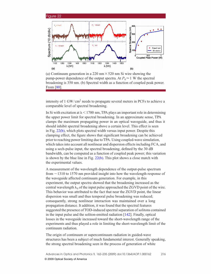
ic
Itcsicpwubit
AftecTdcpsilec
Tst
(pbF
A
©
ntensity of 1 GW/cm2 needs to propagate several meters in PCFs to achieve aomparable level of spectral broadening.
n Si with excitation at ��1700 nm, TPA plays an important role in determininghe upper power limit for spectral broadening. In an approximate sense, TPAlamps the maximum propagating power in an optical waveguide, and thus ithould inhibit spectral broadening above a certain level. This effect is seenn Fig. 22(b), which plots spectral width versus input power. Despite thislamping effect, the figure shows that significant broadening can be achievedrior to reaching power limiting due toTPA. Using coupled-wave simulation,hich takes into account all nonlinear and dispersion effects including FCA, andsing a sech-pulse input, the spectral broadening, defined by the 30 dBandwidth, can be computed as a function of coupled peak power; this variations shown by the blue line in Fig. 22(b). This plot shows a close match withhe experimental values.
measurement of the wavelength dependence of the output-pulse spectrumrom �1310 to 1570 nm provided insight into how the wavelength response ofhe waveguide affected continuum generation. For example, in thisxperiment, the output spectra showed that the broadening increased as theentral wavelength �0 of the input pulse approached the ZGVD point of the wire.his behavior was attributed to the fact that near the ZGVD point, the linearispersion was small and thus temporal pulse broadening was reduced;onsequently, strong nonlinear interaction was maintained over a longropagation distance. It addition, it was found that the spectral featuresuggested the presence of TOD-induced spectral separation of solitons containedn the input pulse and the soliton-emitted radiation [142]. Finally, opticalosses in the waveguide increased toward the short-wavelength range of thexperiments and thus played a role in limiting the short-wavelength limit of theontinuum radiation.
he origin of continuum or supercontinuum radiation in guided-wavetructures has been a subject of much fundamental interest. Generally speaking,
Figure 22
a) Continuum generation in a 220 nm�520 nm Si wire showing theump-power dependence of the output spectra. At P0�1 W the spectralroadening is 350 nm. (b) Spectral width as a function of coupled peak power.rom [80].
he strong spectral broadening seen in the process of generation of white
dvances in Optics and Photonics 1, 162–235 (2009) doi:10.1364/AOP.1.000162 216
2009 Optical Society of America

lntpfc[ro[delmn�tfraspptapnpbe
7
Opcpsfe
PtfSfTait
Xp
A
©
ight (supercontinuum radiation) is attributable to the onset of (cascaded)onlinear effects. The particular details of the evolution from the input-pulse tohe output-pulse spectrum are strongly dependent on the specific pulsearameters, such as pulse width, pulse peak power, pulse chirp, and carrierrequency, as well as the linear and nonlinear optical properties of theorresponding optical medium [104]. In addition, higher-order-soliton fission126,128,129,160,161] can be dominant in the initial stages of supercontinuumadiation generation. In fact, it is apparent that soliton effects, as recentlybserved in Si wires [73] and previously known to be important in fiber optics101], can also serve as the source of significant spectral broadening. Clearly,ispersive effects are important in continuum generation. To increase thefficiency of the supercontinuum-generation process, input pulses may beaunched near the ZGVD point so that the optical dispersion is small and thusinimizes temporal pulse broadening, which reduces the strength of the
onlinear effects. In the presence of dispersion, the sign of the GVD coefficient
2 determines which phenomena are important for continuum generation. Inhe first case, when the pulse propagates in the normal dispersion regime, i.e.,or �20, the main nonlinear processes that contribute to the supercontinuumadiation are FWM, intrapulse Raman scattering, and, to a smaller extent, SPMnd MI. However, in this normal dispersion regime, FWM processes havemall efficiency at wavelengths far from the pump input [162] owing to the poorhase-matching characteristics and become even less efficient as the peakower increases. In addition, if femtosecond pulses are used, as was the case inhe experiment just described, the Raman interaction in Si would be weak,s the characteristic Raman response time in Si is in the range of a fewicoseconds. As a result, spectral broadening of pulses propagating in theormal dispersion regime is expected to be small. By contrast, for pulsesropagating in the anomalous dispersion regime, �2�0, both FWM and MI cane strongly phase matched, and thus both nonlinear optical processes becomefficient in generating new optical frequencies.
.2. Spectral Manipulation of Pulses Using Si Photonic Wires
ne of the simplest applications of optical fibers is the use of their dispersiveroperties to vary the spectral and temporal content of guided-wave pulses. Thelassic application is the wide use of dispersion-shifted fiber to correct forulse broadening in a fiber link [101]. This same approach has been used inelf-mode-locked ring lasers [163]. More elaborate schemes can be used and inact have recently attracted much interest because of the dispersionngineering possible in microstructured fiber [89].
ulse temporal manipulation can also be accomplished with SPW, except inhis case integration of the fiber is nearly impossible. Pulse compressionunctionality can be achieved in millimeter-long devices implemented in thisOI platform. Thus, recently, Chen et al. demonstrated theoretically foremtosecond pulses that dispersion engineering in conjunction with SPM andOD can be used to achieve pulse compression [96]. In addition, Tien etl. experimentally demonstrated pulse compression in Si waveguides; althoughn this case the dispersion from photogenerated carriers was used to providehe necessary waveguide dispersive profile [164].
PM can also provide an active optically controlled pulse-compression
rocess. In this approach, a strong pump modifies the phase experienced by thedvances in Optics and Photonics 1, 162–235 (2009) doi:10.1364/AOP.1.000162 217
2009 Optical Society of America

psdlipppau2pGrp
7
FasTcdarniblfira
S�asoi
A
©
robe or signal beam and thus generates additional bandwidth that can supporthorter pulses. Compression requires that the SPW exhibit anomalousispersion at the probe wavelength. In addition, the pump–probe interactionength must be equal to or larger than the waveguide length. The first requirementmplies that the group velocity of the two pulses is sufficiently close that therobe pulse interacts with the pump over the full length of the waveguide. In therocess, the probe bandwidth is increased via XPM interaction with theump and then is compressed temporally as the probe propagates in thenomalous GVD waveguide. These effects can be numerically simulated bysing the coupled-mode model discussed above. In the example shown in Fig.3, the waveguide is dispersion engineered such that the probe and theump pulses have the same group velocity but have negative and positiveVDs, respectively. The figure shows that SPW enables compression in a
elative short waveguide; that is, for a propagation length of just 0.8 mm therobe pulse yields compression by a factor of �5.
.3. Signal Regeneration Using Four-Wave Mixing
WM has several immediate applications in data communications. Thesepplications include amplification as mentioned above, as well as other morepecific functions. The first of these is signal regeneration and reshaping [165].his functionality requires that a nonlinear relation exist between input andonverted data. Thus regeneration and reshaping has been successfullyemonstrated by using semiconductor amplifiers and FWM in conventionalnd microstructured optical fiber [166–168]. However, as discussed above in thiseview, a nonlinear relation should of course also apply for the case ofonlinear optical processes in a SPW. In fact, nonlinear signal-timingmprovement was demonstrated previously by using a simple Si photodetectorased on TPA [169]. The attractive feature about using SPWs is the extremelyarge n2 within this medium, and thus it is a very basic demonstration ofber-on-a-chip functionality. Use of FWM as the means for accomplishingegeneration also means that ultrabroadband signals can be amplified by usingdispersion-engineered SPW.
Figure 23
imulation of pulse compression as a result of XPM in a h�w=220 nm360 nm Si wire. Signal (left) and pump (right) field envelopes versus time
nd propagation distance. The temporal width is 200 fs for both the pump and theignal pulses. Here �psPp�100 cm−1 for the pump, with a center frequencyf 1625 nm. For the signal Ps�Pp, and its center frequency is 1451 nm. Insets,nitial and final pulse envelopes. From [37].
dvances in Optics and Photonics 1, 162–235 (2009) doi:10.1364/AOP.1.000162 218
2009 Optical Society of America

TiaNtAli1wsibet�cc
7
TpicfsrEluh5w
Ac
Bc
Cc
Dc
mt
A
©
here are several basic approaches to regeneration based on FWM, whichnvolve interchanging the signal, pump, and idler between a CW source or clocknd the input and converted data; these configurations are shown in Table 2.ote that certain of these configurations do not result in the required nonlinear
ransformation between signal and converted data and thus are not of interest.s an example, the most useful configuration for improving timing jitter is the
ast shown in the table, in which the “pump” is the clock, and the input datas the “signal.” This approach was analyzed and experiments performed on a.8 cm length of a 300 nm�500 nm cross-section SPW [165]. With thisire, the authors found a 2.2 reduction in the timing jitter of a gigabit per
econd, return-to-zero data stream using the last configuration. In addition,mprovements in the extinction ratio and pulse reshaping were demonstratedy using the second and third configurations mentioned in Table 2. In the case ofrror recovery, a 4.3 dB improvement was measured in the same SPW and athe same data rate as just described. In this case, the input peak power levels were
100 mW to prevent saturation. Finally, in the case of reshaping,ompensation for the pulse broadening incurred by propagation in aonventional fiber link by the SPW was demonstrated.
.4. On-Chip Data Communication
he quality and compact dimensions of Si-wire photonic integrated circuitsrovide the technology for making on-chip and chip-to-chip SPWnterconnection networks possible [170,171]. Optical transmission and WDMan allow high modulation rates and wavelength parallelism. This capabilityor reaching large bandwidth suggests that high-performance computingystems can now use integrated optics. However, designing such a networkequires that the performance of such interconnects must be well known.xperiments have shown that low-loss Si-wire-waveguide technology has the
inear and nonlinear optical performance for on-chip networks to carryltrahigh-bandwidth WDM data streams. For example, one set of experimentsas demonstrated low-error transmission of a 1.28 Tb/s stream through acm long wire waveguide, with the aggregate data rate, composed of 32avelengths, each modulated at 40 Gbits/ s [172].
Table 2. Use of Four Wavelength Configurations Based on FWM Wavelength-Conversion Signal-Regeneration Schemes in a SPW for Three Wavelengths
�1 ,�2 ,�3 Where �1��2��3a
ConfigurationPulse
ReshapingER
ImprovementTiming Jitter
Reduction
. Input data, CW source,onverted data
✗ ✗ ✗
. CW source, input data,onverted data)
3 3 ✗
. Clock, input data,onverted data
3 3 3
. Input data, clock,onverted data
3 ✗ 3
aSchemes C and D are demonstrated by Salem et al. in [165]. Overall, scheme C isost effective; however, scheme D yields greater jitter reduction than scheme C. Table after
hat in [165].
dvances in Optics and Photonics 1, 162–235 (2009) doi:10.1364/AOP.1.000162 219
2009 Optical Society of America

Tca1s�bfWpa
7S
NadmocolrFtpdsc
7
Gsoostph
AscRrwr
A
©
he instrumentation for the bit error ratio (BER) measurements used 24 CWommunications lasers with 100 GHz channel spacing and outputs combined by32-channel multiplexer. The detected signal was then evaluated at
0 Gbits/ s with a communications signal analyzer and a BER tester. Theignals were transmitted through a SPW, with dimensions h�w=220 nm
520 nm. The 5 cm wire required on-chip path length folding using 24 90°ends, each with a bending radius of 6.5 µm, to achieve the needed smallootprint. Measurements of the output signals showed that in the 5 cm long dense
DM 10 Gbits/ s per wavelength link, the wire exhibited only a 3.3 dBower penalty at a BER of 10−9, or more generally, that a Si-wire can serve assuitable on-chip data conduit.
.5. Broadband Wavelength Conversion of High-Data-Rateignals
onlinear optical conversion has many applications in telecommunications,nd, as a result, a Si wavelength converter is a particularly useful device. Toemonstrate the utility of Si-wire wavelength converters, systemseasurements have been made of the data streams undergoing conversion. In
ne experiment [100], a 10 Gbit/ s non-return-to-zero data train wasonverted across the C band from 1535 to 1566 nm with minimal degradationf the signal quality. This demonstration was accomplished by using theowest-order TM mode of a 300 nm�500 nm waveguide. The C-band tuningange was dictated by the Er-doped fiber amplifier bandwidth and not theWM conversion bandwidth. Eye diagrams of the input signal �1535 nm� and
he converted output �1566 nm� were measured by using a 231−1seudo-random bit sequence and an input signal of −20 dBm. The timeependence of the optical losses such as FCA or thermal effects was sufficientlymall that it caused only minimal degradation of the signal quality of theonverted output, as was also observed in other experiments [63,65,150].
.6. Raman Pulse Delay
eneration of tunable all-optical pulse delays is an important functionality foreveral types of photonic integrated circuit, including creating tunablen-chip optical dispersion. This approach has generally relied on the use ofptical resonances that are available in optical cavities or photonic crystaltructures, which have a very narrow wavelength response. Further, tuning ofhese structures is generally accomplished by relatively slow-responsehenomena such as thermal changes in indices of refraction, and thus theyave only a small temporal bandwidth.
nother approach uses the gain and line shape from stimulated Ramancattering in a Si wire to form an intensity-dependent delay structure, whichan be tuned instantaneously [173]. This approach relies on the fact that theaman-gain curve is related to the refractive index via the Kramers–Krönig
elation. Further, the group index, which determines the speed of a signal pulseithin a guided-wave structure, is related to the refractive index through the
elation
ng��� = n��� + �dn
. �49�
d�dvances in Optics and Photonics 1, 162–235 (2009) doi:10.1364/AOP.1.000162 220
2009 Optical Society of America

TotcRm
wtp
Wasacapdsctpt
8
TobtId
DR
A
©
he total Raman amplification experienced by a signal beam, that is, the ratiof the output signal power Pout to the input signal power Pin, is related tohe gain parameter, G, via Pout /Pin=eG. This Raman contribution to the gainauses a refractive index change as a function of wavelength. For example, at theaman peak, the total delay TD of the signal pulse in passing through theaterial due to the presence of the pump field can be shown to be [173]
TD =G
�R
, �50�
here G=gRIpL is the Raman gain parameter, Ip is the pump intensity, and L ishe length of the interaction region. Because G depends linearly on theump intensity, the delay can then also be tuned by varying the pump power.
ith this approach, tunable optical pulse delays have been achieved by the gainvailable via stimulated Raman scattering [173] in an 8 mm long Si wire ashown in Fig. 24. In the case of the Raman line shape, the delay can be generatedt any wavelength below the bandgap of Si and is widely tunable simply byhanging the wavelength of the pump. In addition, the Si Raman linewidth hasbandwidth that can support a typical (~picosecond) telecommunicationulse. Group index changes of �0.15 may be used to generate �3 ps pulseelays. This method allows the delay of each pulse within a pulse train to beeparately controlled for bandwidths of �100 GHz; a single waveguidean also be used to produce delays at different wavelength channels across theelecommunications spectrum. Last, the short interaction length andump-power-dependent delay allows this scheme to have a fast reconfigurationime of �70 GHz.
. Conclusion
his review has discussed previous and current work on linear and nonlinearptical effects in Si photonic wires (SPWs), a field that is now growing rapidlyecause of the many compelling, new guided-wave optical phenomena andhe many important emerging applications in nonlinear integrated Si photonics.n particular, many recent experimental and theoretical studies haveemonstrated the intertwining of dispersion and optical nonlinearities with
Figure 24
ata taken for SRS-induced delays. Measured delay versus the measuredaman gain parameter. From Okawachi et al. [173].
dvances in Optics and Photonics 1, 162–235 (2009) doi:10.1364/AOP.1.000162 221
2009 Optical Society of America

pfitwnfdpvSncofdfwgppi
A
A
©
articular emphasis on self- and cross-phase modulation from picosecond toemtosecond pulses in Si wires. The theoretical component of this works particularly important, since several physical properties of Si wires, such ashe large index contrast, crystallinity, and tight optical confinement—hich give rise to the potential for dispersion engineering and enhancedonlinear optical effects—make the physics of propagation in Si wires distinctrom those in optical fibers. As a consequence of engineering of thisispersion, photonic wires can be designed to operate as nonlinear devices andarametric mixers with gain over a wide range of group-velocity dispersionalues at telecommunications wavelengths. More generally, by operatingi wires in a regime where the waveguide, characteristic dispersion, andonlinear lengths are comparable with one another, it is possible to probe theomplex interplay among dispersion and nonlinearity at low peak powersf the order of a few hundreds of milliwatts and with waveguide lengths of aew millimeters. In addition, the extremely small Si-wire cross-sectionalimension provides further scaling down of the length�power product requiredor nonlinear optical functionalities from that in standard integrated opticsaveguides. This scale down arises from both the reduced area and the reducedroup velocity of the optical waves. The low threshold powers forhase-changing effects and parametric functionality in SPWs make themotential candidates for various functional nonlinear optical devices in anntegrated platform.
ppendix A: Acronym GlossaryBER = Bit-error ratio
BERT = Bit-error ratio testerBOX = Buried oxide
CARS = Coherent anti-Stokes Ramanscattering
CMOS = Complementary metal-oxidesemiconductor
CSA = Communications signal analyzerCW = Continuous wave
EDFA = Erbium-doped fiber amplifierFC = Free carrier
FCA = Free-carrier absorptionFOM = Figure of merit
FWHM = Full width at half-maximumFWM = Four-wave mixingGVD = Group-velocity dispersion
HPCS = High-performance computingsystems
MI = Modulation instabilityNRZ = Non-return to zeroPCF = Photonic crystal fibersPIC = Photonic integrated circuitsRZ = Return to zero
SMF = Single-mode fiberSOI = Silicon on insulator
SPW = Silicon photonic wireSRS = Stimulated Raman scattering
TE = Transverse electric
dvances in Optics and Photonics 1, 162–235 (2009) doi:10.1364/AOP.1.000162 222
2009 Optical Society of America

A
A
©
TM = Transverse magneticTOD = Third-order dispersionTPA = Two-photon absorption
WDM = Wavelength division multiplexingXPM = Cross-phase modulation
ZGVD = Zero group-velocity dispersion
ppendix B: Symbol Glossarya, b, c, d = Unit vectors
A, B = Sellmeier parametersA0 = Waveguide cross section
Aeff = Effective modal area� = Polarizability tensor
�ij,� = Matrix elements of polarizabilitytensor
�, �in = Absorption coefficient�FC = Free-carrier absorption coefficient
BWFWM = Conversion bandwidth speed oflight
� = Mode propagation constant�1 = First-order dispersion coefficient�2 = Second-order dispersion coefficient�3 = Third-order dispersion coefficient
�TPA = Two-photon absorption coefficient�TPA,wg = Effective two-photon absorption
coefficient��3�, �ijkl
�3� = Third-order optical susceptibility��n� = nth-order optical susceptibility�R = Raman susceptibilityD = Group-velocity dispersion
coefficientD = Electric displacement� = Normalized temporal walk-off
�nFC = Free-carrier-induced change in therefractive index,
�PL = Variation in the linear polarization��L = Variation in the dielectric constant��s = Frequency shift�� = Relative soliton radiation shift� = Phase mismatch
ktotal = Phase mismatchTD = Total delay of signal pulse� = Raman linewidth� = Raman frequency shift
E = Electric fielde�r� ,�� = Electric field of waveguide modes
Eig = Indirect bandgap energy� = Dielectric constant
��r�� = Transverse profile of the dielectricconstant,
�0 = Vacuum permittivity�i = Idler conversion efficiency
dvances in Optics and Photonics 1, 162–235 (2009) doi:10.1364/AOP.1.000162 223
2009 Optical Society of America

A
©
�max,i = FWM maximum efficiencyg = Parametric gain
gR = Stimulated Raman scatteringcoefficient
G = Gain parameterG��� = Modulation instability gain
spectrum�ij = Cross-phase modulation
nonlinearity coefficient�p = Pump nonlinearity coefficient�s = Signal nonlinearity coefficient
� ,�i = Effective nonlinear opticalwaveguide susceptibility
�ij = Effective cross-phase modulationwaveguide susceptibility
�R = Raman gain linewidthh = Waveguide height width
h�r� ,�� = Magnetic field of waveguide modesH = Magnetic field� = Reduced Planck’s constant
kp, ks, ki = Propagation constants of the pump,signal, and idler
� = Modal overlap integral coefficientL = Interaction length
LD = Second-order dispersion lengthLD� = Third-order dispersion lengthLNL = Nonlinear length
� = Wavelength�p = Pump wavelength�s = Signal wavelength�c = Average or mean wavelength
�o+ = Four-wave mixing idler wavelength� = Wave vector of the modulation
instability processm
ce* = Electron effective mass
mch* = Hole effective mass
m0 = Electron massµe = Electron mobilityµh = Hole mobilityn = Index of refraction of Si
n�r�� = Transverse profile of the refractiveindex
n2 = Nonlinear refractive index, Kerrcoefficient
n2,wg = Waveguide effective nonlinear Kerrcoefficient
ncladding = Refractive index of claddingneff = Effective indexng = Group indexN = Carrier density
Nsoliton = Soliton number�P = Pump frequency
dvances in Optics and Photonics 1, 162–235 (2009) doi:10.1364/AOP.1.000162 224
2009 Optical Society of America

A
©
�R = Raman signal frequency� = Photon angular frequency
�0± = Four-wave mixing idler outputfrequencies
�CARS = Coherent anti-Stokes Ramanscattering signal frequency
�p = Pump angular frequency�R = Raman frequency�r = Normalized angular frequency
separation�s, = Stokes angular frequency or signal
angular frequency�� = Raman mode frequency
�s�z ,T� = Nonlinear phase shiftP = Electric polarization
P�z , t� = Position- and time-dependentwaveguide power
P0 = Input peak optical powerPp = Input peak pump powerPs = Input peak signal power
Peff = Effective pump powerPin,s = Signal input power
Pout,i = Idler output powerPR = Raman signal powerPL = Linear polarization
PNL = Nonlinear polarizationS�� , � = Pulse spectrogram
t = Cladding thicknessT = Time in the reference frame of the
pump pulsetc = Carrier lifetime
Td = Temporal delay between two pulsesTp, T0 = Pulse width
0 = Shock time due to bulk nonlinearityresponse
d = Normalized time delay i = Imaginary part of wm
r = Real part of wm
s = Shock time wm = Shock time due to waveguide
contribution = Response time of Raman interaction = Normalized time
u�z , t� = Normalized field amplitudeup�z , t� = Pump normalized field amplitudeus�z , t� = Signal normalized field amplitude
vg = Group velocityvg,s = Signal group velocityvg,p = Pump group velocity
w = Waveguide widthZ0 = Impedance of the free space
dvances in Optics and Photonics 1, 162–235 (2009) doi:10.1364/AOP.1.000162 225
2009 Optical Society of America

A
T(FoA
R
1
1
1
1
A
©
cknowledgments
his research was supported by the Air Force Office of Scientific ResearchUSAFOSR) Small Business Technology Transfer Program, contractA9550-05-C-1954, and by AFOSR grant FA9550-05-1-0428. The IBM partf this work was supported by Office of Naval Research (ONR) /Defensedvanced Research Agency (DARPA) grant N00014-07-C-0105 ONR/DARPA.
eferences
1. L. O. Hocker, D. R. Sokoloff, V. Daneu, A. Szoke, and A. Javan, “Frequencymixing in infrared and far-infrared using a metal-to-metal point contactdiode,” Appl. Phys. Lett. 12, 401–402 (1968).
2. R. M. Roth, N.-C. Panoiu, M. M. Adams, R. M. Osgood, Jr., C. C.Neacsu, and M. B. Raschke, “Resonant-plasmon field enhancement fromasymmetrically illuminated conical metallic-probe tips,” Opt. Express14, 2921–2931 (2006).
3. M. M. Fejer, G. A. Magel, D. H. Jundt, and R. L. Byer,“Quasi-phase-matched second harmonic generation: tuning andtolerances,” IEEE J. Quantum Electron. 28, 2631–2654 (1992).
4. X. Li, K. Terabe, H. Hatano, and K. Kitamura, “Nano-domain engineeringin LiNbO3 by focused ion beam,” Jpn. J. Appl. Phys. Part 1 44, L1550–L1552 (2005).
5. A. Nahata, R. A. Linke, T. Ishi, and K. Ohashi, �Enhanced nonlinearoptical conversion from a periodically nanostructured metal film,� Opt.Lett. 28, 423–425 (2003).
6. M. Airola, Y. Liu, and S. J. Blair, “Second-harmonic generation from anarray of sub-wavelength metal apertures,” J. Opt. A 7, S118–S123(2005).
7. W. Fan, S. Zhang, N.-C. Panoiu, A. Abdenour, S. Krishna, R. M. Osgood,Jr., K. J. Malloy, and S. R. J. Brueck, “Second harmonic generationfrom a nanopatterned isotropic nonlinear material,” Nano Lett. 6, 1027–1030 (2006).
8. W. Fan, S. Zhang, K. J. Malloy, R. J. Brueck, N.-C. Panoiu, and R. M.Osgood, Jr., “Second harmonic generation from patterned GaAs inside asubwavelength metallic hole array,” Opt. Express 14, 9570–9575(2006).
9. R. A. Soref and J. P. Lorenzo, “Single-crystal silicon: a new material for1.3 and 1.6 µm integrated-optical components,” Electron. Lett. 21, 953–954 (1985).
0. R. A. Soref and B. R. Bennett, “Electro-optical effects in silicon,” IEEE J.Quantum Electron. QE-23, 123–129 (1987).
1. A. Liu, R. Jones, L. Liao, D. Samara-Rubio, D. Rubin, O. Cohen, R.Nicolaescu, and M. Paniccia, “A high-speed silicon optical modulator basedon a metal-oxide-semiconductor capacitor,” Nature 427, 615–618(2004).
2. Q. Xu, B. Shmidt, S. Pradhan, and M. Lipson, “Micrometre-scale siliconelectro-optic modulator,” Nature 435, 325–327 (2005).
3. V. R. Almeida, C. A. Barrios, R. Panepucci, and M. Lipson, “All-opticalcontrol of light on a silicon chip,” Nature 431, 1081–1084 (2004).
dvances in Optics and Photonics 1, 162–235 (2009) doi:10.1364/AOP.1.000162 226
2009 Optical Society of America

1
1
1
1
1
1
2
2
2
2
22
2
2
2
2
3
3
3
A
©
4. C. A. Barrios, V. R. de Almeida, and M. Lipson, “Low-power-consumptionshort-length and high-modulation-depth silicon electrooptic modulator,”J. Lightwave Technol. 21, 1089–1098 (2003).
5. G. Cocorullo, M. Iodice, I. Rendina, and P. M. Sarro, “Silicon thermoopticmicromodulator with 700-kHz–3-dB bandwidth,” IEEE Photon.Technol. Lett. 7, 363–365 (1995).
6. R. L. Espinola, M.-C. Tsai, J. T. Yardley, and R. M. Osgood, Jr., “Fast andlow-power thermooptic switch on thin silicon-on-insulator,” IEEEPhoton. Technol. Lett. 15, 1366–1368 (2003).
7. M. Harjanne, M. Kapulainen, T. Aalto, and P. Heimala, “Sub-µs switchingtime in silicon-on-insulator Mach–Zehnder thermooptic switch,” IEEEPhoton. Technol. Lett. 16, 2039–2041 (2004).
8. M. W. Geis, S. J. Spector, R. C. Williamson, and T. M. Lyszczarz,“Submicrosecond, submilliwatt, silicon-on-insulator thermooptic switch,”IEEE Photon. Technol. Lett. 16, 2514–2516 (2004).
9. Y. A. Vlasov, M. O’Boyle, H. F. Hamann, and S. J. McNab, “Activecontrol of slow light on a chip with photonic crystal waveguides,” Nature438, 65–69 (2005).
0. W. Bogaerts, R. Baets, P. Dumon, V. Wiaux, S. Beckx, D. Taillaert, B.Luyssaert, J. van Campenhout, P. Bienstman, and D. van Thourhout,“Nanophotonic waveguides in silicon-on-insulator fabricated with CMOStechnology,” J. Lightwave Technol. 23, 401–412 (2005).
1. R. A. Soref, “Silicon-based optoelectronics,” Proc. IEEE 81, 1687–1706(1993).
2. B. P. Pal, “Guided-wave optics on silicon: physics, technology and status,”in Progress in Optics, Volume XXXII, E.Wolf, ed. (Elsevier, 1993), pp. 3–59.
3. G. T. Reed and A. P. Knights, Silicon Photonics: an Introduction (Wiley,2004).
4. L. Pavesi and D. J. Lockwood, Silicon Photonics (Springer-Verlag, 2004).5. M. Paniccia, M. Morse, and M. Salib, “Integrated photonics,” Top. Appl.
Phys. 94, 51–88 (2004).6. L. C. Kimerling, L. Dal Negro, S. Saini, Y. Yi, D. Ahn, S. Akiyama, D.
Cannon, J. Liu, J. G. Sandland, D. Sparacin, J. Michel, K. Wada, and M. R.Watts, “Monolithic silicon microphotonics,” Top. Appl. Phys. 94, 89–120 (2004).
7. B. Jalali, R. Claps, D. Dimitropoulos, and V. Raghunathan, “Lightgeneration, amplification, and wavelength conversion via stimulated Ramanscattering in silicon microstructures,” Top. Appl. Phys. 94, 199–238(2004).
8. R. J. Bozeat, S. Day, F. Hopper, F. P. Payne, S. W. Roberts, and M.Asghari, “Silicon based waveguides,” Top. Appl. Phys. 94, 269–294 (2004).
9. S. Janz, “Silicon-based waveguide technology for wavelength divisionmultiplexing,” Top. Appl. Phys. 94, 323–360 (2004).
0. A. Irace, G. Breglio, M. Iodice, and A. Cutolo, “Light modulation withsilicon devices,” Top. Appl. Phys. 94, 361–391 (2004).
1. M. Lipson, “Guiding, modulating, and emitting light on silicon—challenges and opportunities,” J. Lightwave Technol. 23, 4222–4238(2005).
2. L. Pavesi and G. Guillot, Optical Interconnects—the Silicon Approach(Springer-Verlag, 2006).
dvances in Optics and Photonics 1, 162–235 (2009) doi:10.1364/AOP.1.000162 227
2009 Optical Society of America

3
3
3
3
3
3
3
4
4
4
4
4
4
4
4
4
4
5
A
©
3. B. Jalali and S. Fathpour, “Silicon photonics,” J. Lightwave Technol. 24,4600–4615 (2006).
4. R. A. Soref, “The past, present, and future of silicon photonics,” IEEE J.Sel. Top. Quantum Electron. 12, 1678–1687 (2006).
5. P. Dumon, G. Priem, L. R. Nunes, W. Bogaerts, D. van Thourhout, P.Bienstman, T. K. Liang, M. Tsuchiya, P. Jaenen, S. Beckx, J. Wouters, andR. Baets, “Linear and nonlinear nanophotonic devices based onsilicon-on-insulator wire waveguides,” Jpn. J. Appl. Phys. Part 1 45, 6589–6602 (2006).
6. R. Dekker, N. Usechak, M. Först, and A. Driessen, “Ultrafast nonlinearall-optical processes in silicon-on-insulator waveguides,” J. Phys. D40, R249–R271 (2007).
7. J. I. Dadap, N. C. Panoiu, X. Chen, I. Hsieh, X. Liu, C. Chou, E. Dulkeith,S. J. McNab, F. Xia, W. M. J. Green, L. Sekaric, Y. A. Vlasov, and R.M. Osgood, Jr., “Nonlinear-optical phase modification indispersion-engineered Si photonic wires,” Opt. Express 16, 1280–1299(2008).
8. M. A. Foster, A. C. Turner, M. Lipson, and A. L. Gaeta, “Nonlinear opticsin photonic nanowires,” Opt. Express 16, 1300–1320 (2008).
9. Q. Lin, O. J. Painter, and G. P. Agrawal, “Nonlinear optical phenomena insilicon waveguides: modeling and applications,” Opt. Express 15,16604–16644 (2007).
0. R. Claps, D. Dimitropoulos, Y. Han, and B. Jalali, “Observation of Ramanemission in silicon waveguides at 1.54 µm,” Opt. Express 10, 1305–1313 (2002).
1. J. I. Dadap, R. L. Espinola, R. M. Osgood, Jr., S. J. McNab, and Y. A.Vlasov, “Spontaneous Raman scattering in ultrasmall silicon waveguides,”Opt. Lett. 29, 2755–2757 (2004).
2. R. Claps, D. Dimitropoulos, V. Raghunathan, Y. Han, and B. Jalali,“Observation of stimulated Raman amplification in silicon waveguides,”Opt. Express 11, 1731–1739 (2003).
3. R. Espinola, J. I. Dadap, R. M. Osgood, S. J. McNab, and Y. A. Vlasov,“Raman amplification in ultrasmall silicon-on-insulator wire waveguides,”Opt. Express 12, 3713–3718 (2004).
4. T. K. Liang and H. K. Tsang, “Efficient Raman amplification insilicon-on-insulator waveguides,” Appl. Phys. Lett. 85, 3343–3345 (2004).
5. A. Liu, H. Rong, M. Paniccia, O. Cohen, and D. Hak, “Net optical gain ina low loss silicon-on-insulator waveguide by stimulated Ramanscattering,” Opt. Express 12, 4261–4268 (2004).
6. Ö. Boyraz and B. Jalali, “Demonstration of 11 dB fiber-to-fiber gain in asilicon Raman amplifier,” IEICE Electron. Express 1, 429–434 (2004).
7. Q. Xu, V. R. Almeida, and M. Lipson, “Demonstration of high Ramangain in a submicrometer-size silicon-on-insulator waveguide,” Opt. Lett. 30,35–37 (2005).
8. R. Claps, V. Raghunathan, Ö. Boyraz, P. Koonath, D. Dimitropoulos, andB. Jalali, “Raman amplification and lasing in SiGe waveguides,” Opt.Express 13, 2459–2466 (2005).
9. S. G. Cloutier, P. A. Kossyrev, and J. Xu, “Optical gain and stimulatedemission in periodic nanopatterned crystalline silicon,” Nat. Mater. 4, 887–891 (2005).
0. J. F. McMillan, X. Yang, N. C. Panoiu, R. M. Osgood, and C. W. Wong,
dvances in Optics and Photonics 1, 162–235 (2009) doi:10.1364/AOP.1.000162 228
2009 Optical Society of America

5
5
5
5
5
5
5
5
5
6
6
6
6
6
6
6
6
6
A
©
“Enhanced stimulated Raman scattering in slow-light photonic crystalwaveguides,” Opt. Lett. 31, 1235–1237 (2006).
1. Ö. Boyraz and B. Jalali, “Demonstration of a silicon Raman laser,” Opt.Express 12, 5269–5273 (2004).
2. H. Rong, A. Liu, R. Jones, O. Cohen, D. Hak, R. Nicolaescu, A. Fang, andM. Paniccia, “An all-silicon Raman laser,” Nature 433, 292–294 (2005).
3. H. Rong, R. Jones, A. Liu, O. Cohen, D. Hak, A. Fang, and M. Paniccia,“A continuous-wave Raman silicon laser,” Nature 433, 725–728(2005).
4. Ö. Boyraz and B. Jalali, “Demonstration of a directly modulated siliconRaman laser,” Opt. Express 13, 796–800 (2005).
5. H. Rong, Y.-H. Kuo, S. Xu, A. Liu, R. Jones, M. Paniccia, O. Cohen, andO. Raday, “Monolithic integrated Raman silicon laser,” Opt. Express14, 6705–6712 (2006).
6. A. Polman, B. Min, J. Kalkman, T. J. Kippenberg, and K. J. Vahala,“Ultra-low threshold erbium-implanted toroidal microlaser on silicon,”Appl. Phys. Lett. 84, 1037–1039 (2004).
7. A. W. Fang, H. Park, O. Cohen, R. Jones, M. J. Paniccia, and J. E. Bowers,“Electrically pumped hybrid AlGaInAs–silicon evanescent laser,” Opt.Express 14, 9203–9210 (2006).
8. R. Claps, V. Raghunathan, D. Dimitropoulos, and B. Jalali, “Anti-StokesRaman conversion in silicon waveguides,” Opt. Express 11, 2862–2872 (2003).
9. V. Raghunathan, R. Claps, D. Dimitropoulos, and B. Jalali, “ParametricRaman wavelength conversion in scaled silicon waveguides,” J. LightwaveTechnol. 23, 2094–2102 (2005).
0. R. Espinola, J. Dadap, R. Osgood, Jr., S. McNab, and Y. Vlasov, “C-bandwavelength conversion in silicon photonic wire waveguides,” Opt.Express 13, 4341–4349 (2005).
1. H. Fukuda, K. Yamada, T. Shoji, M. Takahashi, T. Tsuchizawa, T.Watanabe, J.-i. Takahashi, and S.-i. Itabashi, “Four-wave mixing in siliconwire waveguides,” Opt. Express 13, 4629–4637 (2005).
2. Q. Xu, V. R. Almeida, and M. Lipson, “Micrometer-scale all-opticalwavelength converter on silicon,” Opt. Lett. 30, 2733–2735 (2005).
3. Y.-H. Kuo, H. Rong, V. Sih, S. Xu, M. Paniccia, and O. Cohen,“Demonstration of wavelength conversion at 40 Gb/s data rate in siliconwaveguides,” Opt. Express 14, 11721–11726 (2006).
4. M. A. Foster, A. C. Turner, J. E. Sharping, B. S. Schmidt, M. Lipson, andA. L. Gaeta, “Broadband optical parametric gain on a silicon photonicchip,” Nature 441, 960–963 (2006).
5. K. Yamada, H. Fukuda, T. Tsuchizawa, T. Watanabe, T. Shoji, and S.Itabashi, “All-optical efficient wavelength conversion using siliconphotonic wire waveguide,” IEEE Photon. Technol. Lett. 18, 1046–1048(2006).
6. Q. Lin, J. Zhang, P. M. Fauchet, and G. P. Agrawal, “Ultrabroadbandparametric generation and wavelength conversion in silicon waveguides,”Opt. Express 14, 4786–4799 (2006).
7. H. K. Tsang, C. S. Wong, T. K. Lang, I. E. Day, S. W. Roberts, A. Harpin,J. Drake, and M. Asghari, “Optical dispersion, two-photon absorptionand self-phase modulation in silicon waveguides at 1.5 µm wavelength,”Appl. Phys. Lett. 80, 416–418 (2002).
8. G. W. Rieger, K. S. Virk, and J. F. Young, “Nonlinear propagation of
dvances in Optics and Photonics 1, 162–235 (2009) doi:10.1364/AOP.1.000162 229
2009 Optical Society of America

6
7
7
7
7
7
7
7
7
7
7
8
88
8
8
A
©
ultrafast 1.5 µm pulses in high-index-contrast silicon-on-insulatorwaveguides,” Appl. Phys. Lett. 84, 900–902 (2004).
9. Ö. Boyraz, T. Indukuri, and B. Jalali, “Self-phase modulation-inducedspectral broadening in silicon waveguides,” Opt. Express 12, 829–834(2004).
0. A. Cowan, G. Rieger, and J. Young, “Nonlinear transmission of 1.5 µmpulses through single-mode silicon-on-insulator waveguide structures,”Opt. Express 12, 1611–1621 (2004).
1. H. Yamada, M. Shirane, T. Chu, H. Yokoyama, S. Ishida, and Y. Arakawa,“Nonlinear-optic silicon-nanowire waveguides,” Jpn. J. Appl. Phys.,Part 1 44, 6541–6545 (2005).
2. E. Dulkeith, Y. A. Vlasov, X. Chen, N. C. Panoiu, and R. M. Osgood, Jr.,“Self-phase-modulation in submicron silicon-on-insulator photonicwires,” Opt. Express 14, 5524–5534 (2006).
3. I.-W. Hsieh, X. Chen, J. I. Dadap, N. C. Panoiu, R. M. Osgood, S. J.McNab, and Y. A. Vlasov, “Ultrafast-pulse self-phase modulation andthird-order dispersion in Si photonic wire-waveguides,” Opt. Express 14,12380–12387 (2006).
4. Ö. Boyraz, P. Koonath, V. Raghunathan, and B. Jalali, “All opticalswitching and continuum generation in silicon waveguides,” Opt. Express12, 4094–4102 (2004).
5. T. Liang, L. Nunes, T. Sakamoto, K. Sasagawa, T. Kawanishi, M.Tsuchiya, G. Priem, D. Van Thourhout, P. Dumon, R. Baets, and H. Tsang,“Ultrafast all-optical switching by cross-absorption modulation insilicon wire waveguides,” Opt. Express 13, 7298–7303 (2005).
6. R. Dekker, A. Driessen, T. Wahlbrink, C. Moormann, J. Niehusmann, andM. Först, “Ultrafast Kerr-induced all-optical wavelength conversion insilicon waveguides using 1.55 µm femtosecond pulses,” Opt. Express 14,8336–8346 (2006).
7. I.-W. Hsieh, X. Chen, J. I. Dadap, N. C. Panoiu, R. M. Osgood, Jr., S. J.McNab, and Y. A. Vlasov, “Cross-phase modulation-induced spectral andtemporal effects on co-propagating femtosecond pulses in siliconphotonic wires,” Opt. Express 15, 1135–1146 (2007).
8. C. Manolatou and M. Lipson, “All-optical silicon modulators based oncarrier injection by two-photon absorption,” J. Lightwave Technol.24, 1433–1439 (2006).
9. T. K. Liang, L. R. Nunes, M. Tsuchiya, K. S. Abedin, T. Miyazaki, D. VanThourhout, W. Bogaerts, P. Dumon, R. Baets, and H. K. Tsang, “Highspeed logic gate using two-photon absorption in silicon waveguides,” Opt.Commun. 265, 171–174 (2006).
0. I.-W. Hsieh, X. Chen, X. Liu, J. I. Dadap, N. C. Panoiu, C.-Y. Chou, F.Xia, W. M. Green, Y. A. Vlasov, and R. M. Osgood, “Supercontinuumgeneration in silicon photonic wires,” Opt. Express 15, 15242–15249(2007).
1. R. W. Boyd, Nonlinear Optics, 2nd ed. (Academic, 2002).2. R. Ahmad, F. Pizzuto, G. S. Camarda, R. L. Espinola, H. Rao, and R. M.
Osgood, Jr., “Ultra-compact corner-mirrors and T-branches insilicon-on-insulator.” IEEE Photon. Technol. Lett. 14, 65–67 (2002).
3. S. McNab, N. Moll, and Y. A. Vlasov, “Ultra-low loss photonic integratedcircuit with membrane-type photonic crystal waveguides,” Opt. Express11, 2927–2939 (2003).
4. Y. Vlasov and S. McNab, “Losses in single-mode silicon-on-insulator
dvances in Optics and Photonics 1, 162–235 (2009) doi:10.1364/AOP.1.000162 230
2009 Optical Society of America

8
8
8
8
8
9
9
9
9
9
9
9
9
9
91
11
A
©
strip waveguides and bends,” Opt. Express 12, 1622–1631 (2004).5. T. Shoji, T. Tsuchizawa, T. Watanabe, K. Yamada, and H. Morita, “Low
loss mode size converter from 0.3 µm square Si wire waveguides tosinglemode fibres,” Electron. Lett. 38, 1669–1670 (2002).
6. V. R. Almeida, R. R. Panepucci, and M. Lipson, “Nanotaper for compactmode conversion,” Opt. Lett. 28, 1302–1304 (2003).
7. F. Xia, L. Sekaric, and Y. A. Vlasov, “Ultracompact optical buffers on asilicon chip,” Nat. Photonics 1, 65–71 (2007).
8. C. G. Poulton, C. Koos, M. Fujii, A. Pfrang, T. Schimmel, J. Leuthold,and W. Freude, “Radiation modes and roughness loss in high index-contrastwaveguides,” IEEE J. Sel. Top. Quantum Electron. 12, 1306–1321(2006).
9. W. H. Reeves, D. V. Skryabin, F. Biancalana, J. C. Knight, P. S. J. Russell,F. G. Omenetto, A. Efimov, and A. J. Taylor, “Transformation andcontrol of ultra-short pulses in dispersion-engineered photonic crystalfibers,” Nature 424, 511–515 (2003).
0. M. Foster, K. Moll, and A. Gaeta, “Optimal waveguide dimensions fornonlinear interactions,” Opt. Express 12, 2880–2887 (2004).
1. S. Ramachandran, “Dispersion-tailored few-mode fibers: a versatileplatform for in-fiber photonic devices,” J. Lightwave Technol. 23, 3426–3443 (2005).
2. X. Chen, N. C. Panoiu, and R. M. Osgood, “Theory of Raman-mediatedpulsed amplification in silicon-wire waveguides,” IEEE J. QuantumElectron. 42, 160–170 (2006).
3. E. Dulkeith, F. Xia, L. Schares, W. M. J. Green, and Y. A. Vlasov, “Groupindex and group velocity dispersion in silicon-on-insulator photonicwires,” Opt. Express 14, 3853–3863 (2006).
4. A. C. Turner, C. Manolatou, B. S. Schmidt, M. Lipson, M. A. Foster, J. E.Sharping, and A. L. Gaeta, “Tailored anomalous group-velocitydispersion in silicon channel waveguides,” Opt. Express 14, 4357–4362(2006).
5. L. Yin, Q. Lin, and G. P. Agrawal, “Dispersion tailoring and solitonpropagation in silicon waveguides,” Opt. Lett. 31, 1295–1297 (2006).
6. X. Chen, N. Panoiu, I. Hsieh, J. I. Dadap, and R. M. Osgood, Jr.,“Third-order dispersion and ultrafast pulse propagation in silicon wirewaveguides,” IEEE Photon. Technol. Lett. 18, 2617–2619 (2006).
7. X. Liu, W. M. J. Green, X. Chen, I-W. Hsieh, J. I. Dadap, Y. A. Vlasov,and R. M. Osgood, Jr., “Conformal dielectric overlayers for engineeringdispersion and effective nonlinearity of silicon nanophotonic wires,”Opt. Lett. 33, 2889–2891 (2008).
8. W. M. J. Green, X. Liu, X. Chen, S. Assefa, R. M. Osgood, Jr., and Y. A.Vlasov, “Dispersion engineering of silicon nanophotonic wires usinga thin film cladding,” in Conference on Lasers and Electro-Optics/QuantumElectronics and Laser Science Conference and Photonic ApplicationsSystems Technologies, OSA Technical Digest (CD) (Optical Society ofAmerica, 2008), paper CTuDD5.
9. E. D. Palik, Handbook of Optical Constants of Solids (Academic, 1998).00. M. A. Foster, A. C. Turner, R. Salem, M. Lipson, and A. L. Gaeta,
“Broad-band continuous-wave parametric wavelength conversion insilicon nanowaveguides,” Opt. Express 15, 12949–12958 (2007).
01. G. P. Agrawal, Nonlinear Fiber Optics (Academic, 2006).02. I. P. Kaminow and T. L. Koch, Optical Fiber Telecommunications IIIA
dvances in Optics and Photonics 1, 162–235 (2009) doi:10.1364/AOP.1.000162 231
2009 Optical Society of America

1
1
1
1
1
1
1
1
1
1
1
1
1
1
1
1
1
1
1
1
A
©
(Academic, 1997).03. J. Lou, L. Tong, and Z. Ye, “Dispersion shifts in optical nanowires with
thin dielectric coatings,” Opt. Express 14, 6993–6998 (2006).04. J. M. Dudley, G. Genty, and S. Coen, “Supercontinuum generation in
photonic crystal fiber,” Rev. Mod. Phys. 78, 1135–1184 (2006).05. J. M. Dudley, G. Genty, and B. J. Eggleton, “Harnessing and control of
optical rogue waves in supercontinuum generation,” Opt. Express16, 3644–3651 (2008).
06. K. K. Tsia, S. Fathpour, and B. Jalali, “Electrical control of parametricprocesses in silicon waveguides,” Opt. Express 16, 9838–9843 (2008).
07. J. Zhang, Q. Lin, G. Piredda, R. W. Boyd, G. P. Agrawal, and P. M.Fauchet, “Anisotropic nonlinear response of silicon in the near-infraredregion,” Appl. Phys. Lett. 91, 071113 (2007).
08. M. Dinu, F. Quochi, and H. Garcia, “Third-order nonlinearities in siliconat telecom wavelengths,” Appl. Phys. Lett. 82, 2954 (2003).
09. M. Dinu, “Dispersion of phonon-assisted nonresonant third-ordernonlinearities,” IEEE J. Quantum Electron. 39, 1498–1503 (2003).
10. A. D. Bristow, N. Rotenberg, and H. M. van Driel, “Two-photonabsorption and Kerr coefficients of silicon for 850–2200 nm,” Appl.Phys. Lett. 90, 191104 (2007).
11. Q. Lin, J. Zhang, G. Piredda, R. W. Boyd, P. M. Fauchet, and G. P.Agrawal, “Dispersion of silicon nonlinearities in the near infrared region,”Appl. Phys. Lett. 91, 021111 (2007).
12. H. Garcia and R. Kalyanaraman, “Phonon-assisted two-photon absorptionin the presence of a dc-field: the nonlinear Franz–Keldysh effect inindirect gap semiconductors,” J. Phys. B 39, 2737–2746 (2006).
13. P. A. Temple and C. E. Hathaway, “Multiphonon Raman spectrum ofsilicon,” Phys. Rev. B 7, 3685–3697 (1973).
14. Y. R. Shen and N. Bloembergen, “Theory of stimulated Brillouin andRaman scattering,” Phys. Rev. 137, A1787–A1805 (1965).
15. M. D. Levenson and N. Bloembergen, “Dispersion of the nonlinearsusceptibility tensor in centrosymmetric media,” Phys. Rev. B 10, 4447–4464 (1974).
16. M. Cardona, “Resonance phenomena,” in Light Scattering in Solids II,Vol. 50 of Topics in Applied Physics, M. Cardona and G. Guntherodt, eds.(Springer, 1982), Chap. 2.
17. H. Vogt, “Coherent and hyper-Raman techniques,” in Light Scattering inSolids II, Vol. 50 of Topics in Applied Physics, M. Cardona and G.Guntherodt, eds. (Springer, 1982), Chap. 4.
18. R. Loudon, “The Raman effect in crystals,” Adv. Phys. 50, 813–864(2001).
19. P. E. Barclay, K. Srinivasan, and O. Painter, “Nonlinear response ofsilicon photonic crystal microresonators excited via an integratedwaveguide and fiber taper,” Opt. Express 13, 801–820 (2005).
20. A. W. Snyder and J. D. Love, Optical Waveguide Theory (Chapman &Hall, 1983).
21. M. J. Adams, S. Ritchie, and M. J. Robertson, “Optimum overlap ofelectric and optical fields in semiconductor waveguide devices,” Appl.Phys. Lett. 48, 820–822 (1986).
22. S. R. Giguere, L. Friedman, R. A. Soref, and J. P. Lorenzo, “Simulationstudies of silicon electro-optic waveguide devices,” J. Appl. Phys.68, 4964–4970 (1990).
dvances in Optics and Photonics 1, 162–235 (2009) doi:10.1364/AOP.1.000162 232
2009 Optical Society of America

1
1
1
1
1
1
1
1
1
1
1
1
1
1
1
1
1
1
1
A
©
23. T. K. Liang and H. K. Tsang, “Role of free carriers from two-photonabsorption in Raman amplification in silicon-on-insulator waveguides,”Appl. Phys. Lett. 84, 2745–2747 (2004).
24. R. Claps, V. Raghunathan, D. Dimitropoulos, and B. Jalali, “Influence ofnonlinear absorption on Raman amplification in Silicon waveguides,”Opt. Express 12, 2774–2780 (2004).
25. C. Koos, L. Jacome, C. Poulton, J. Leuthold, and W. Freude, “Nonlinearsilicon-on-insulator waveguides for all optical signal processing,”Opt. Express 15, 5976–5990 (2007).
26. P. K. A. Wai, C. R. Menyuk, Y. C. Lee, and H. H. Chen, “Nonlinear pulsepropagation in the neighborhood of the zero-dispersion wavelength ofmonomode optical fibers,” Opt. Lett. 11, 464–466 (1986).
27. P. K. A. Wai, C. R. Menyuk, Y. C. Lee, and H. H. Chen, “Soliton at thezero-group-dispersion wavelength of a single mode fiber,” Opt. Lett. 12,628–630 (1987).
28. P. K. A. Wai, H. H. Chen, and Y. C. Lee, “Radiations by solitons at thezero group-dispersion wavelength of single-mode optical fibers,” Phys.Rev. A 41, 426–439 (1990).
29. N. Akhmediev and M. Karlsson, “Cherenkov radiation emitted bysolitons in optical fibers,” Phys. Rev. A 51, 2602–2607 (1995).
30. J. Santhanam and G. P. Agrawal, “Raman-induced spectral shifts inoptical fibers: general theory based on the moment method,” Opt.Commun. 222, 413–420 (2003).
31. L. A. Ostrovskii, “Propagation of wave packets and space-timeself-focusing in a nonlinear medium,” Sov. Phys. JETP 24, 797 (1967).
32. D. Grischkowsky, E. Courtens, and J. A. Armstrong, “Observation ofself-steepening of optical pulses with possible shock formation,” Phys.Rev. Lett. 31, 422–425 (1973).
33. N. Tzoar and M. Jain, “Self-phase modulation in long-geometryoptical-waveguides,” Phys. Rev. A 23, 1266–1270 (1981).
34. E. A. Golovchenko, E. M. Dianov, A. M. Prokhorov, and V. N. Serkin,“Decay of optical solitons,” JETP Lett. 42, 87–91 (1985).
35. N. C. Panoiu, X. Liu, and R. M. Osgood, “Self-steepening of ultrashortpulses in Si photonic nanowires” to be submitted to Opt. Lett.
36. B. Kibler, J. M. Dudley, and S. Coen, “Supercontinuum generation andnonlinear pulse propagation in photonic crystal fiber: influence ofthe frequency-dependent effective mode area,” Appl. Phys. B 81, 337–342 (2005).
37. N. C. Panoiu, X. Chen, and R. M. Osgood, Jr., “Modulation instability insilicon photonic nanowires,” Opt. Lett. 31, 3609–3611 (2006).
38. Y. Liu and H. K. Tsang, “Nonlinear absorption and Raman gain inhelium-ion-implanted silicon waveguides,” Opt. Lett. 31, 1714–1716(2006).
39. R. Jones, H. Rong, A. Liu, A. Fang, M. Paniccia, D. Hak, and O. Cohen,“Net continuous wave optical gain in a low loss silicon-on-insulatorwaveguide by stimulated Raman scattering,” Opt. Express 13, 519–525(2005).
40. M. Krause, H. Renner, S. Fathpour, B. Jalali, and E. Brinkmeyer, “Gainenhancement in cladding-pumped silicon raman amplifiers,” IEEE J.Quantum Electron. 44, 692–704 (2008).
41. J. Zhang, Q. Lin, G. Piredda, R. W. Boyd, G. P. Agrawal, and P. M.
dvances in Optics and Photonics 1, 162–235 (2009) doi:10.1364/AOP.1.000162 233
2009 Optical Society of America

1
1
1
1
1
1
1
1
1
1
1
1
1
1
1
1
1
A
©
Fauchet, “Optical solitons in a silicon waveguide,” Opt. Express 15, 7682–7688 (2007).
42. L. Yin and G. P. Agrawal, “Soliton fission and supercontinuum generationin silicon waveguides,” Opt. Lett. 32, 391–393 (2007).
43. L. Ding, C. Benton, A. V. Gorbach, L. Ding, W. J. Wadsworth, J. C.Knight, D. V. Skryabin, M. Gnan, M. Sorrel, and R. M. De La Rue,“Solitons and spectral broadening in long silicon-on-insulator photonicwires,” Opt. Express 16, 3310–3319 (2008).
44. P. F. Curley, C. Spielmann, T. Brabec, F. Krausz, E. Wintner, and A. J.Schmidt, “Operation of a femtosecond Ti:sapphire solitary laser in thevicinity of zero group-delay dispersion,” Opt. Lett. 18, 54–56 (1993).
45. P. L. Baldeck, R. R. Alfano, and G. P. Agrawal, “Induced-frequency shiftof copropagating ultrafast optical pulses,” Appl. Phys. Lett. 52, 1939–1941 (1988).
46. K. W. DeLong, K. B. Rochford, and G. I. Stegeman, “Effect of two-photonabsorption on all-optical guided wave devices,” Appl. Phys. Lett. 55,1823–1825 (1989).
47. J. Hansryd, A. Andrekson, M. Westlund, J. Li, and P. Hedekvist,“Fiber-based optical parametric amplifiers and their applications,” IEEEJ. Sel. Top. Quantum Electron. 8, 506–520 (2002).
48. J. D. Harvey, R. Leonhardt, S. Coen, G. K. L. Wong, J. C. Knight, W. J.Wadsworth, and P. St. J. Russell, “Scalar modulation instability inthe normal dispersion regime by use of a photonic crystal fiber,” Opt.Lett. 28, 2225–2227 (2003).
49. T. V. Andersen, K. M. Hilligsoe, C. K. Nielsen, J. Thogersen, K. P.Hansen, S. R. Keidling, and J. J. Larsen, “Continuous-wave wavelengthconversion in a photonic crystal fiber with two zero-dispersionwavelengths,” Opt. Express 12, 4113–4122 (2004).
50. H. Rong, Y.-H. Kuo, A. Liu, M. Paniccia, and O. Cohen, “High efficiencywavelength conversion of 10 Gb/s data in silicon waveguides,” Opt.Express 14, 1182–1188 (2006).
51. G. P. Agrawal, “Modulation instability induced by cross-phasemodulation,” Phys. Rev. Lett. 59, 880–883 (1987).
52. J. E. Rothenberg, “Modulational instability for normal dispersion,” Phys.Rev. A 42, 682–685 (1990).
53. W. Huang and J. Hong, “A coupled-mode analysis of modulationinstability in optical fibers,” J. Lightwave Technol. 10, 156–162 (1992).
54. M. Yu, C. J. Mckinstrie, and G. P. Agrawal, “Instability due to cross-phasemodulation in the normal-dispersion regime,” Phys. Rev. E 48, 2178–2186 (1993).
55. D. Schadt and B. Jaskorzynska, “Generation of short pulses from CWlight by influence of crossphase modulation (CPM) in optical fibres,”Electron. Lett. 23, 1090–1091 (1987).
56. A. S. Gouveia-Neto, M. E. Faldon, A. S. B. Sombra, P. G. J. Wigley, andJ. R. Taylor, “Subpicosecond-pulse generation throughcross-phase-modulation-induced modulational instability in opticalfibers,” Opt. Lett. 13, 901–903 (1988).
57. W. Drexler, “Ultrahigh-resolution optical coherence tomography,” J.Biomed. Opt. 9, 47–74 (2004).
58. A. V. Husakou and J. Herrmann, “Supercontinuum generation ofhigher-order solitons by fission in photonic crystal fibers,” Phys. Rev.Lett. 87, 203901–203904 (2001).
dvances in Optics and Photonics 1, 162–235 (2009) doi:10.1364/AOP.1.000162 234
2009 Optical Society of America

1
1
1
1
1
1
1
1
1
1
1
1
1
1
1
A
©
59. M. A. Foster, J. M. Dudley, B. Kibler, Q. Cao, D. Lee, R. Trebino, and A.L. Gaeta, “Nonlinear pulse propagation and supercontinuum generationin photonic nanowires: experiment and simulation,” Appl. Phys. B81, 363–367 (2005).
60. Y. S. Kivshar and B. A. Malomed, “Dynamics of solitons in nearlyintegrable systems,” Rev. Mod. Phys. 61, 763–916 (1989).
61. Y. Kodama and A. Hasegawa, “Nonlinear pulse propagation in amonomode dielectric guide,” IEEE J. Quantum Electron. 23, 510–524(1987).
62. A. Demircan and U. Bandelow, “Analysis of the interplay betweensoliton fission and modulation instability in supercontinuum generation,”Appl. Phys. B 86, 31–39 (2007).
63. H. A. Haus, “Short pulse lasers,” in Compact Sources of UltrashortPulses, I. N. Duling III, ed. (Cambridge U. Press, 1995).
64. E.-K. Tien, N. S. Yuksek, F. Qian, and Ö. Boyraz, “Pulse compressionand modelocking by using TPA in silicon waveguides,” Opt. Express 15,6500–6506 (2007).
65. R. Salem, M. A. Foster, A. C. Turner, D. F. Geraghty, M. Lipson, and A.L. Gaeta, “Signal regeneration using low-power four-wave mixing onsilicon chip,” Nat. Photonics 2, 35–38 (2008).
66. M. Rochette, L. Fu, V. Ta’eed, D. J. Moss, and B. J. Eggleton, “2R opticalregeneration: an all-optical solution for BER improvement,” IEEE J.Sel. Top. Quantum Electron. 12, 736–744 (2006).
67. H. Simos, A. Bogris, and D. Syvridis, “Investigation of a 2R all-opticalregenerator based on four-wave mixing in a semiconductor opticalamplifier,” IEEE Photon. Technol. Lett. 22, 595–597 (2004).
68. J. Suzuki, T. Tanemura, K. Taira, Y. Ozeki, and K. Kikuchi, “All-opticalregenerator using wavelength shift induced by cross-phase modulationin highly nonlinear dispersion-shifted fiber,” IEEE Photon. Technol. Lett.17, 423–425 (2005).
69. R. Salem, G. E. Tudury, T. U. Horton, G. M. Carter, and T. E. Murphy,“Polarization-insensitive optical clock recovery at 80 Gb/s using a siliconphotodiode” IEEE Photon. Technol. Lett. 17, 1968–1970 (2005).
70. D. A. B. Miller, “Rationale and challenges for optical interconnects toelectronic chips,” Proc. IEEE 88, 728–749 (2000).
71. A. Shacham, K. Bergman, and L. P. Carloni, “On the design of aphotonic network-on-chip,” in Proceedings of the IEEE InternationalSymposium on Networks-on-Chip (NOCS ’07) (IEEE, 2007), paper 2.1.
72. B. G. Lee, X. G. Chen, A. Biberman, X. P. Liu, I. W. Hsieh, C. Y. Chou,J. I. Dadap, F. N. Xia, W. M. J. Green, L. Sekaric, Y. A. Vlasov, R.M. Osgood, and K. Bergman, “Ultrahigh-bandwidth silicon photonicnanowire waveguides for on-chip networks” IEEE Photon. Technol. Lett.20, 398–400 (2008).
73. Y. Okawachi, M. Foster, J. Sharping, A. Gaeta, Q. Xu, and M. Lipson,“All-optical slow-light on a photonic chip,” Opt. Express 14, 2317–2322(2006).
dvances in Optics and Photonics 1, 162–235 (2009) doi:10.1364/AOP.1.000162 235
2009 Optical Society of America


![[3.4]_Fiber Nonlinearities](https://static.fdocuments.in/doc/165x107/55cf8e81550346703b92da6f/34fiber-nonlinearities.jpg)