
Engineering Department photography competition - IfM entries v2
7
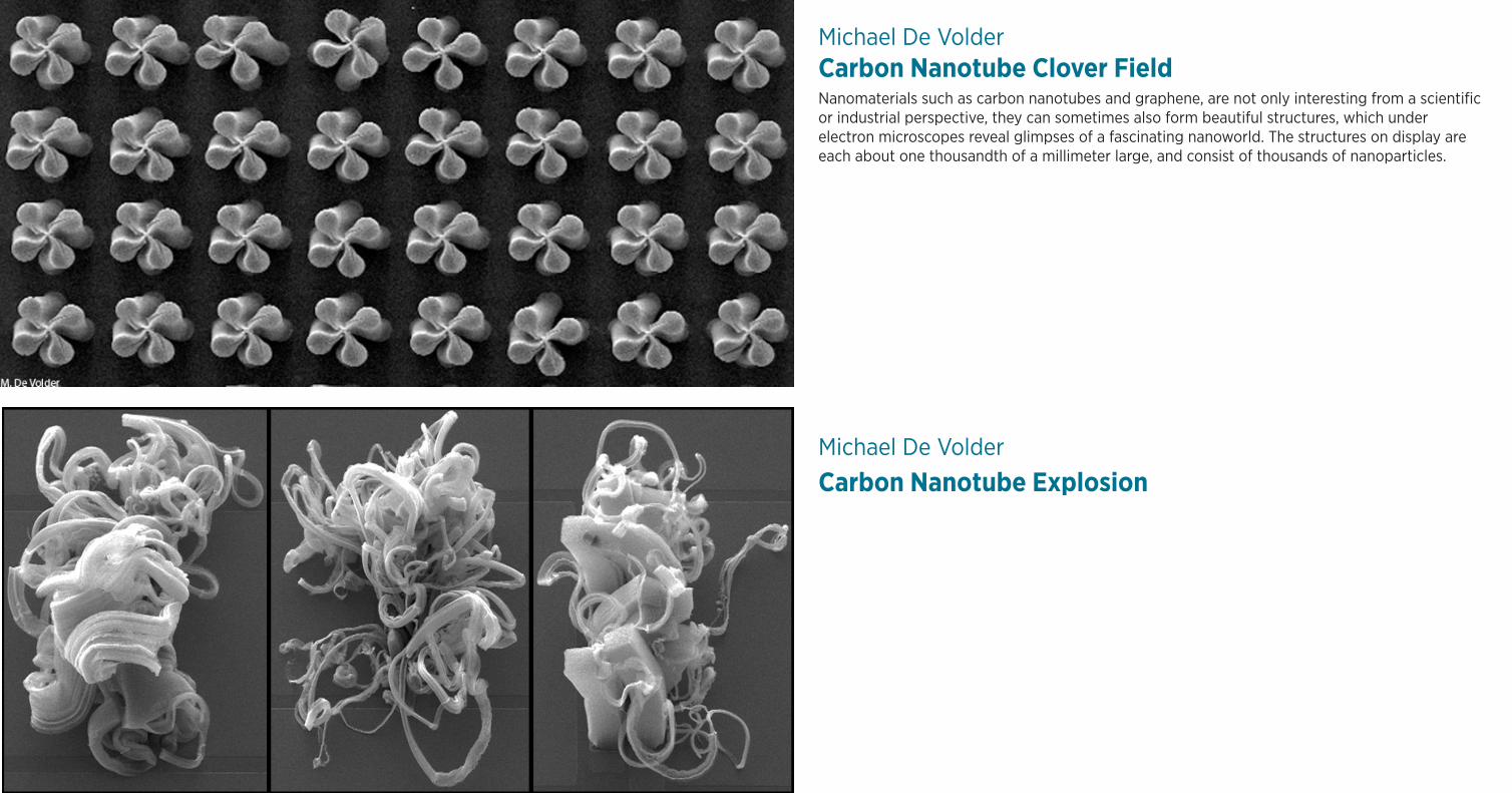
Michael De Volder Carbon Nanotube Clover Field Nanomaterials such as carbon nanotubes and graphene, are not only interesting from a scientific or industrial perspective, they can sometimes also form beautiful structures, which under electron microscopes reveal glimpses of a fascinating nanoworld. The structures on display are each about one thousandth of a millimeter large, and consist of thousands of nanoparticles. Michael De Volder Carbon Nanotube Explosion
-
Upload
ifm-cambridge -
Category
Documents
-
view
225 -
download
2
description
Â
Transcript of Engineering Department photography competition - IfM entries v2
Michael De Volder Carbon Nanotube Clover Field Nanomaterials such as carbon nanotubes and graphene, are not only interesting from a scientific or industrial perspective, they can sometimes also form beautiful structures, which under electron microscopes reveal glimpses of a fascinating nanoworld. The structures on display are each about one thousandth of a millimeter large, and consist of thousands of nanoparticles.
Michael De Volder
Carbon Nanotube Explosion
Michael De Volder
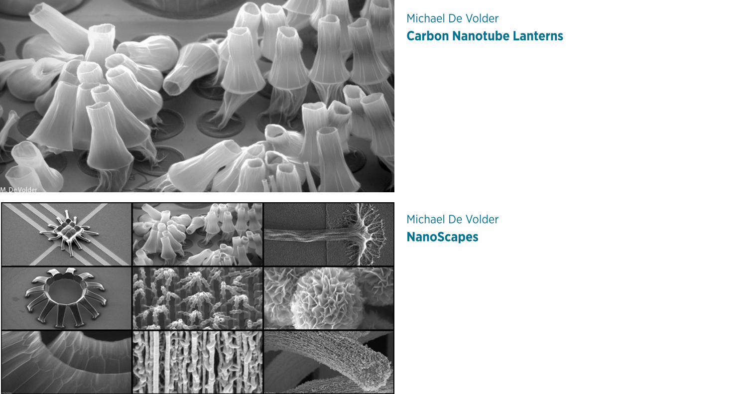
Carbon Nanotube Lanterns
Michael De Volder
NanoScapes
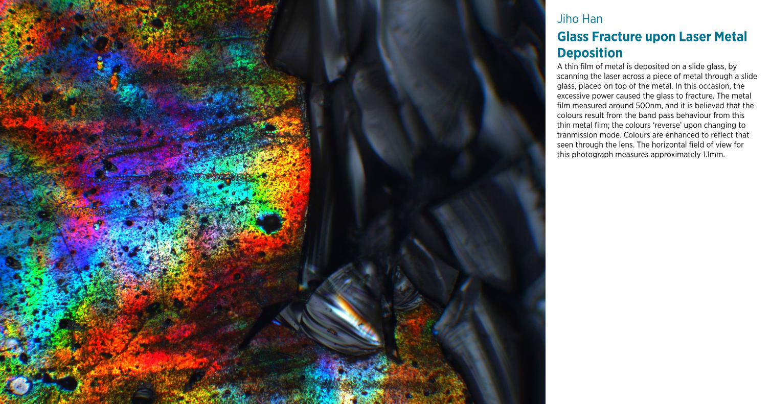
Jiho HanGlass Fracture upon Laser Metal Deposition A thin film of metal is deposited on a slide glass, by scanning the laser across a piece of metal through a slide glass, placed on top of the metal. In this occasion, the excessive power caused the glass to fracture. The metal film measured around 500nm, and it is believed that the colours result from the band pass behaviour from this thin metal film; the colours ‘reverse’ upon changing to tranmission mode. Colours are enhanced to reflect that seen through the lens. The horizontal field of view for this photograph measures approximately 1.1mm.
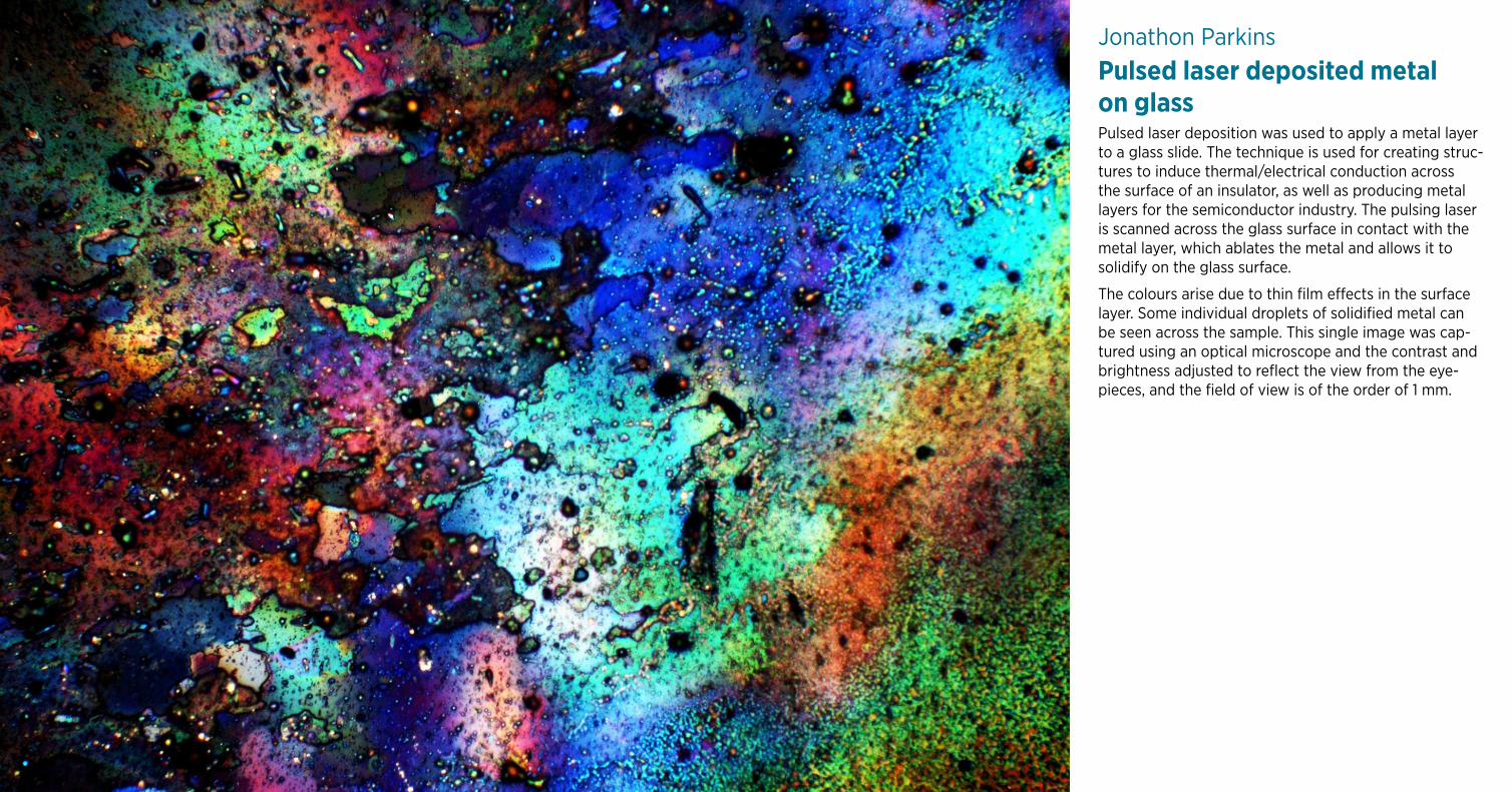
Jonathon ParkinsPulsed laser deposited metal on glass Pulsed laser deposition was used to apply a metal layer to a glass slide. The technique is used for creating struc-tures to induce thermal/electrical conduction across the surface of an insulator, as well as producing metal layers for the semiconductor industry. The pulsing laser is scanned across the glass surface in contact with the metal layer, which ablates the metal and allows it to solidify on the glass surface.
The colours arise due to thin film effects in the surface layer. Some individual droplets of solidified metal can be seen across the sample. This single image was cap-tured using an optical microscope and the contrast and brightness adjusted to reflect the view from the eye-pieces, and the field of view is of the order of 1 mm.
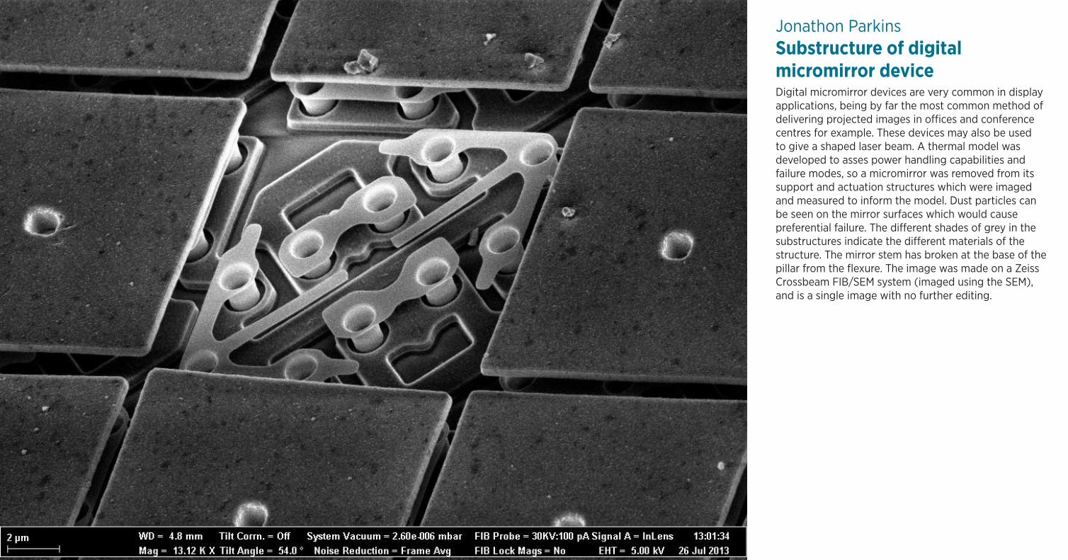
Jonathon Parkins Substructure of digital micromirror device Digital micromirror devices are very common in display applications, being by far the most common method of delivering projected images in offices and conference centres for example. These devices may also be used to give a shaped laser beam. A thermal model was developed to asses power handling capabilities and failure modes, so a micromirror was removed from its support and actuation structures which were imaged and measured to inform the model. Dust particles can be seen on the mirror surfaces which would cause preferential failure. The different shades of grey in the substructures indicate the different materials of the structure. The mirror stem has broken at the base of the pillar from the flexure. The image was made on a Zeiss Crossbeam FIB/SEM system (imaged using the SEM), and is a single image with no further editing.
Jonathon Parkins
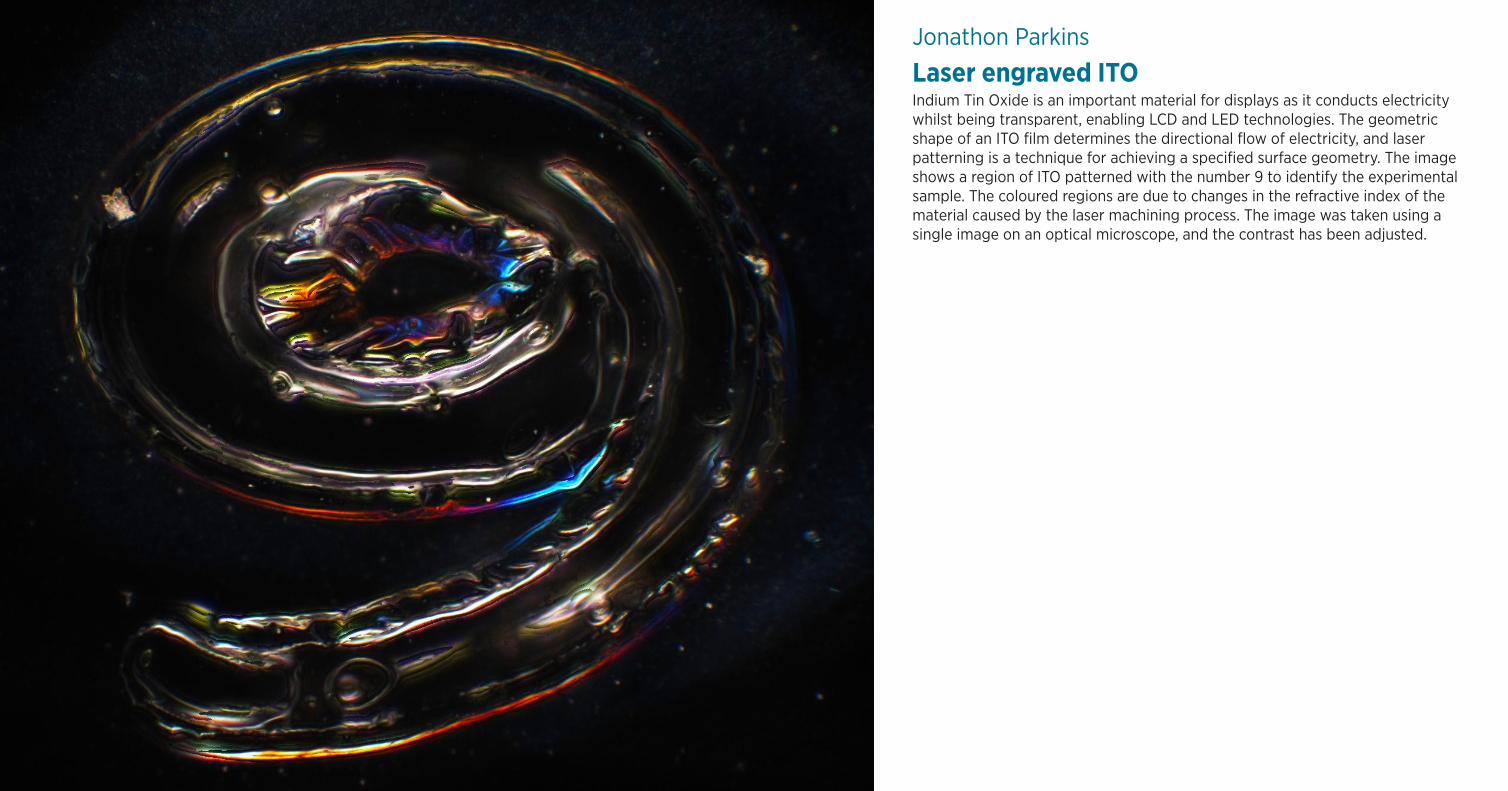
Laser engraved ITO Indium Tin Oxide is an important material for displays as it conducts electricity whilst being transparent, enabling LCD and LED technologies. The geometric shape of an ITO film determines the directional flow of electricity, and laser patterning is a technique for achieving a specified surface geometry. The image shows a region of ITO patterned with the number 9 to identify the experimental sample. The coloured regions are due to changes in the refractive index of the material caused by the laser machining process. The image was taken using a single image on an optical microscope, and the contrast has been adjusted.
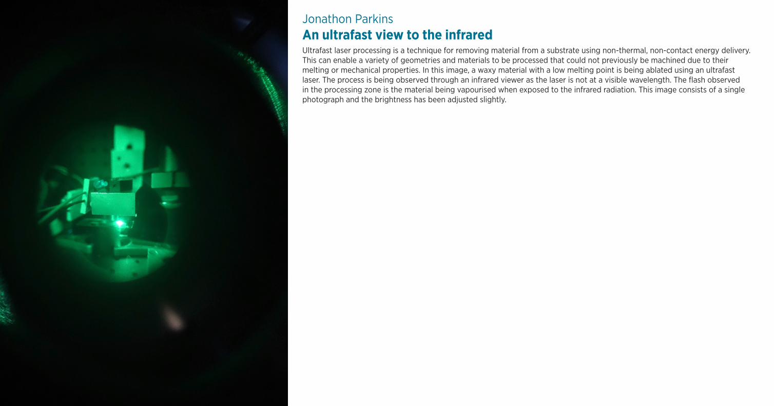
Jonathon ParkinsAn ultrafast view to the infrared Ultrafast laser processing is a technique for removing material from a substrate using non-thermal, non-contact energy delivery. This can enable a variety of geometries and materials to be processed that could not previously be machined due to their melting or mechanical properties. In this image, a waxy material with a low melting point is being ablated using an ultrafast laser. The process is being observed through an infrared viewer as the laser is not at a visible wavelength. The flash observed in the processing zone is the material being vapourised when exposed to the infrared radiation. This image consists of a single photograph and the brightness has been adjusted slightly.