ENGINEERING COLLEGEmahalakshmiengineeringcollege.com/pdf/ece/IVsem/EC2252/UNIT 2.pdf · EC2252 –...
37
EC2252 – COMMUNICATION THEORY, IV Sem ECE – R.Vanitha Asst.Prof./ECE Page 1 MAHALAKSHMI ENGINEERING COLLEGE QUESTION BANK DEPARTMENT: ECE SEMESTER: IV SUBJECT CODE / Name: EC2252 – COMMUNICATION THEORY UNIT-II ANGLE MODULATION SYSTEMS PART- A 1. What is frequency deviation in FM? (AUC NOV 2006) The rate at which the frequency changes are occurring is equal to the frequency of the modulating signal (fm). (Δf) is called the frequency deviation 2. What is narrow band FM? (AUC MAY 2006) When the modulation index is small, the bandwidth ofFM is narrow The bandwidth of narrow band FM is same as that of AM, which is twice that baseband of modulated signal 3. State Carson’s rule. (AUC NOV 2007) Carson’s rule provides a thumb formula to calculate the bandwidth of a single tone wide band FM.According to this rule the FM bandwidth is given as twice the sum of the frequency deviation and the highest modulating frequency. However, it must be remembered that this rule is just an approximation. Mathematically B.W=2(Δf+f m ) Δf – frequency deviation; f m – modulating frequency 4. Define phase modulation. (AUC NOV 2007) It is defined as the process by which the phase of the constant amplitude carrier is varied and directly proportional to amplitude of the modulating signal at a rate equal to the frequency of the modulating signal
Transcript of ENGINEERING COLLEGEmahalakshmiengineeringcollege.com/pdf/ece/IVsem/EC2252/UNIT 2.pdf · EC2252 –...

EC2252 – COMMUNICATION THEORY, IV Sem ECE – R.Vanitha Asst.Prof./ECE Page 1
MAHALAKSHMI ENGINEERING COLLEGE
QUESTION BANK
DEPARTMENT: ECE SEMESTER: IV
SUBJECT CODE / Name: EC2252 – COMMUNICATION THEORY
UNIT-II ANGLE MODULATION SYSTEMS
PART- A
1. What is frequency deviation in FM? (AUC NOV 2006)
The rate at which the frequency changes are occurring is equal to the frequency of the
modulating signal (fm).
(Δf) is called the frequency deviation
2. What is narrow band FM? (AUC MAY 2006)
When the modulation index is small, the bandwidth ofFM is narrow
The bandwidth of narrow band FM is same as that of AM, which is twice that
baseband of modulated signal
3. State Carson’s rule. (AUC NOV 2007)
Carson’s rule provides a thumb formula to calculate the bandwidth of a single tone wide
band FM.According to this rule the FM bandwidth is given as twice the sum of the
frequency deviation and the highest modulating frequency. However, it must be
remembered that this rule is just an approximation.
Mathematically B.W=2(Δf+fm)
Δf – frequency deviation; fm – modulating frequency
4. Define phase modulation. (AUC NOV 2007)
It is defined as the process by which the phase of the constant amplitude carrier is
varied and directly proportional to amplitude of the modulating signal at a rate equal to
the frequency of the modulating signal

EC2252 – COMMUNICATION THEORY, IV Sem ECE – R.Vanitha Asst.Prof./ECE Page 2
5. Mention advantages of angle modulation over amplitude modulation.
(AUC NOV 2008)
The angle modulation has many advantages over amplitude modulation such as noise
reduction, improved system fidelity and more efficient use of power.
6. State the disadvantages of FM. (AUC NOV 2008)
A much wider channel typically 200KHz is required in FM as against only 10kHz,
in AM broadcast. This form serious limitation on FM.
Fm transmitting and receiving equipment particularly used for modulation and
demodulation tend to be more complex and hence costlier.
7. When modulating frequency in an FM system is 500 Hz and modulating voltage is
3V, modulation index is 60. Calculate maximum deviation and bandwidth.
(AUC NOV 2008)
8. Draw the phasor diagram, frequency spectrum of narrowband FM.
(AUC MAY 2004) (AUC NOV 2006) (AUC MAY2010)
9. Define modulation index of the FM wave. (AUC MAY 2013) (AUC MAY 2009)
The modulation index for FM is the ratio of maximum frequency deviation to the
modulating frequency.
10. Differentiate between narrowband FM and Wideband FM(AUC MAY
2009)Distinguish between narrow band FM and wide band FM(AUC MAY 2011)
WIDEBAND FM:
Parameters :
1. modulation index : Greater than 1
2. Maximum deviation: 75 kHz
3. Range of modulating frequency: 30 Hz to 15 kHz
4. Maximum modulation index: 5 to 2500

EC2252 – COMMUNICATION THEORY, IV Sem ECE – R.Vanitha Asst.Prof./ECE Page 3
5. Bandwidth: large, about 15 times higher than BW of narrowband FM
6. applications: entertainment broadcasting
7. Pre-emphasis and de-emphasis: is needed.
NARROWBAND FM:
parameters :
1.modulation index: less than or slightly greater than 1
2. Maximum deviation: 5kHz
3. Range of modulating frequency: 30 Hz to 3 kHz
4. Maximum modulation index: slightly greater than 1
5. Bandwidth: small. Approximately same as that of AM
6. Applications: FM mobile communication like police wireless, ambulance etc
7. Pre-emphasis and de-emphasis: is needed.
11. Obtain the bandwidth of the FM signal
c(t) = 10*cos[2*107*πt + 8 cos(1000*πt)] (AUC MAY 2009)
12. Draw t he block diagram of a method for generating a narrowband FM signal.
(AUC MAY 2010)
We can generate FM signals by using various FM modulators. The basic requirement of
FM modulator (FM signals generator) is to provide a variable output frequency with
varying proportions to the instantaneous amplitude of the modulating voltage. The FM
signals can be generated by two methods
1. Direct Method. The FM signals can be generated directly by frequency modulating the
carrier
2. Indirect Methods. The FM signals’ can be generated indirectly by integrating the
modulating and signal and then allowing it to phase modulate the carrier.
Or by using the modulating signal first to produce a narrow band FM signal and then by
frequency multiplication, the frequency deviation may be increased to the desired level.
13. A carrier wave of frequency 100 MHz is frequency modulated by a signal 20
sin(200π × 103t).what is bandwidth of FM signal if the frequency sensitivity of the
modulation is 25kHz/V (AUC MAY 2010)
ANS:
Fc=100MHz,Vm(t)=20 sin(200π × 103t), Kf=25 KHz/v
AM=20V
∆f=Kf.VM= 25*20V=500KHz

EC2252 – COMMUNICATION THEORY, IV Sem ECE – R.Vanitha Asst.Prof./ECE Page 4
B.W= 2(∆f+fm)=1200KHz
14. What is meant by detection? Name the methods for detecting FM signals
(AUC MAY 2011)
The process of extracting a modulating signal from a modulated carrier signal is called
demodulation or detection
Types of FM
1. Slope detector
2. Phase difference discriminators
15. How is the Narrow band FM converted into wideband FM? (AUC DEC 2011)
FM signal is given by
S(t)=AC Cos(2πfct+βsin2πfmt)
If β is very small compared to one radian, it is called NBFM. If the value of β is very large
compared to 1 radian, it is called wideband FM
16. What are the advantages of Ratio detector? (AUC DEC 2011)
It is not affected by amplitude variation on the FM waves
Phase relationship between primary and secondary of the circuit is linear
17. Illustrate the relationship between FM and PM, with block diagram.(AUC MAY
2012)
18. What is meant by detection? Name the method for detecting FM signal.
(AUC MAY 2012)
The process of extracting a message signal from the modulated signal is called as
detection. The methods for detecting FM signal are
1. Slope detector
simple slope detector
Balanced detector
1. Phase difference detector
Foster seeley detector
Ratio detector
PART- B
EC2252 – COMMUNICATION THEORY, IV Sem ECE – R.Vanitha Asst.Prof./ECE Page 5
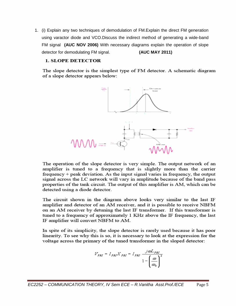
1. (i) Explain any two techniques of demodulation of FM.Explain the direct FM generation
using varactor diode and VCO.Discuss the indirect method of generating a wide-band
FM signal (AUC NOV 2006) With necessary diagrams explain the operation of slope
detector for demodulating FM signal. (AUC MAY 2011)
EC2252 – COMMUNICATION THEORY, IV Sem ECE – R.Vanitha Asst.Prof./ECE Page 6

EC2252 – COMMUNICATION THEORY, IV Sem ECE – R.Vanitha Asst.Prof./ECE Page 7

EC2252 – COMMUNICATION THEORY, IV Sem ECE – R.Vanitha Asst.Prof./ECE Page 8
2. Derive the expression for the frequency modulated signal. Explain what is meant by
narrow band FM and wide band FM using expression. (AUC NOV 2006)

EC2252 – COMMUNICATION THEORY, IV Sem ECE – R.Vanitha Asst.Prof./ECE Page 9

EC2252 – COMMUNICATION THEORY, IV Sem ECE – R.Vanitha Asst.Prof./ECE Page 10

EC2252 – COMMUNICATION THEORY, IV Sem ECE – R.Vanitha Asst.Prof./ECE Page 11
EC2252 – COMMUNICATION THEORY, IV Sem ECE – R.Vanitha Asst.Prof./ECE Page 12
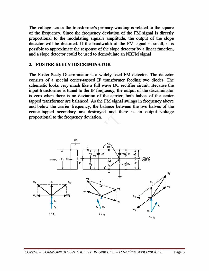
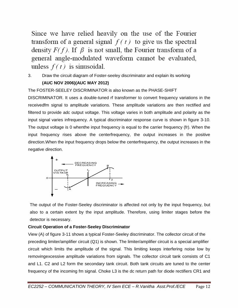
3. Draw the circuit diagram of Foster-seeley discriminator and explain its working
(AUC NOV 2006)(AUC MAY 2012)
The FOSTER-SEELEY DISCRIMINATOR is also known as the PHASE-SHIFT
DISCRIMINATOR. It uses a double-tuned rf transformer to convert frequency variations in the
receivedfm signal to amplitude variations. These amplitude variations are then rectified and
filtered to provide adc output voltage. This voltage varies in both amplitude and polarity as the
input signal varies infrequency. A typical discriminator response curve is shown in figure 3-10.
The output voltage is 0 whenthe input frequency is equal to the carrier frequency (fr). When the
input frequency rises above the centerfrequency, the output increases in the positive
direction.When the input frequency drops below the centerfrequency, the output increases in the
negative direction.
The output of the Foster-Seeley discriminator is affected not only by the input frequency, but
also to a certain extent by the input amplitude. Therefore, using limiter stages before the
detector is necessary.
Circuit Operation of a Foster-Seeley Discriminator
View (A) of figure 3-11 shows a typical Foster-Seeley discriminator. The collector circuit of the
preceding limiter/amplifier circuit (Q1) is shown. The limiter/amplifier circuit is a special amplifier
circuit which limits the amplitude of the signal. This limiting keeps interfering noise low by
removingexcessive amplitude variations from signals. The collector circuit tank consists of C1
and L1. C2 and L2 form the secondary tank circuit. Both tank circuits are tuned to the center
frequency of the incoming fm signal. Choke L3 is the dc return path for diode rectifiers CR1 and

EC2252 – COMMUNICATION THEORY, IV Sem ECE – R.Vanitha Asst.Prof./ECE Page 13
CR2. R1 and R2 are not always necessary but are usually used when the back (reverse bias)
resistance of the two diodes is different. Resistors R3 and R4 are the load resistors and are
bypassed by C3 and C4 to remove rf. C5 is the output coupling capacitor.
CIRCUIT OPERATION AT RESONANCE.—The operation of the Foster-Seeley discriminator
can best be explained using vector diagrams [figure 3-11, view (B)] that show phase
relationships between the voltages and currents in the circuit. Let's look at the phase
relationships when the input frequency is equal to the center frequency of the resonant tank
circuit.
The input signal applied to the primary tank circuit is shown as vector ep. Since coupling
capacitor C8 has negligible reactance at the input frequency, rf choke L3 is effectively in parallel
with the primary tank circuit. Also, because L3 is effectively in parallel with the primary tank
circuit, input voltage epalso appears across L3. With voltage epapplied to the primary of T1, a
voltage is induced in the secondary which causes current to flow in the secondary tank circuit.
When the input frequency is equal to the center frequency, the tank is at resonance and acts
resistive. Current and voltage are in phase in a resistance circuit, as shown by is and ep. The
current flowing in the tank causes voltage drops across each half of the balanced secondary
winding of transformer T1. These voltage drops are of equal amplitude and opposite polarity
with respect to the center tap of the winding. Because the winding is inductive, the voltage
across it is 90 degrees out of phase with the current through it. Because of the center-tap
arrangement, the voltages at each end of the secondary winding of T1 are 180 degrees out of
phase and are shown as e1 and e2 on the vector diagram.

EC2252 – COMMUNICATION THEORY, IV Sem ECE – R.Vanitha Asst.Prof./ECE Page 14
The voltage applied to the anode of CR1 is the vector sum of voltages epand e1, shown as e 3
on the diagram. Likewise, the voltage applied to the anode of CR2 is the vector sum of voltages
epand e 2, shown as e4 on the diagram. At resonance e3 and e4 are equal, as shown by
vectors of the same length. Equal anode voltages on diodes CR1 and CR2 produce equal
currents and, with equal load resistors, equal and opposite voltages will be developed across
R3 and R4. The output is taken across R3 and R4 and will be 0 at resonance since these
voltages are equal and of appositive polarity. The diodes conduct on opposite half cycles of the
input waveform and produce a series of dc pulses at the rf rate. This rf ripple is filtered out by
capacitors C3 and C4.
OPERATION ABOVE RESONANCE.—A phase shift occurs when an input frequency higher
than the center frequency is applied to the discriminator circuit and the current and voltage
phase relationships change. When a series-tuned circuit operates at a frequency above
resonance, the inductive reactance of the coil increases and the capacitive reactance of the
capacitor decreases. Above resonance the tank circuit acts like an inductor. Secondary current
lags the primary tank voltage, ep. Notice that secondary voltages e 1 and e2 are still 180
degrees out of phase with the current (iS) that produces them. The change to a lagging
secondary current rotates the vectors in a clockwise direction. This causes el to become more in
phase with epwhile e2 is shifted further out of phase with ep. The vector sum of epand e2 is less
than that of epand e1. Above the center frequency, diode CR1 conducts more than diode CR2.
Because of this heavier conduction, the voltage developed across R3 is greater than the voltage
developed across R4; the output voltage is positive.
OPERATION BELOW RESONANCE.—When the input frequency is lower than the center
frequency, the current and voltage phase relationships change. When the tuned circuit is
operated at a frequency lower than resonance, the capacitive reactance increases and the
inductive reactance decreases. Below resonance the tank acts like a capacitor and the
secondary current leads primary tank voltage ep. This change to a leading secondary current
rotates the vectors in a counterclockwise direction. From the vector diagram you should see that
e2 is brought nearer in phase with ep, while el is shifted further out of phase with ep. The vector
sum of epand e2 is larger than that of e and e1. Diode CR2 conducts more than diode CR1
below the center frequency. The voltage drop across R4 is larger than that across R3 and the
output across both is negative.
Disadvantages
These voltage outputs can be plotted to show the response curve of the discriminator discussed

EC2252 – COMMUNICATION THEORY, IV Sem ECE – R.Vanitha Asst.Prof./ECE Page 15
earlier (figure 3-10). When weak AM signals (too small in amplitude to reach the circuit limiting
level) pass through the limiter stages, they can appear in the output. These unwanted amplitude
variations will cause primary voltage ep[view (A) of figure 3-11] to fluctuate with the modulation
and to induce a similar voltage in the secondary of T1. Since the diodes are connected as half-
wave rectifiers, these small AM signals will be detected as they would be in a diode detector
and will appear in the output. This unwanted AM interference is cancelled out in the ratio
detector (to be studied next in this chapter) and is the main disadvantage of the Foster-Seeley
circuit.
4. Explain the direct FM generation using varactor diode and VCO (AUC NOV 2007) Explain how
varactor diode can be used for frequency modulation. (AUC NOV 2005)

EC2252 – COMMUNICATION THEORY, IV Sem ECE – R.Vanitha Asst.Prof./ECE Page 16
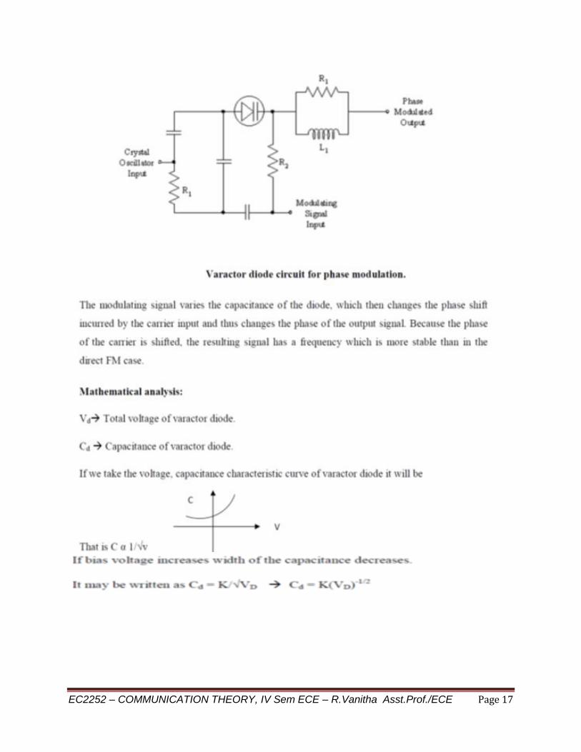
EC2252 – COMMUNICATION THEORY, IV Sem ECE – R.Vanitha Asst.Prof./ECE Page 17

EC2252 – COMMUNICATION THEORY, IV Sem ECE – R.Vanitha Asst.Prof./ECE Page 18
5. Explain in detail about (i) Balanced discriminators (ii) Phase-shift discriminators.
(AUC NOV 2007)

EC2252 – COMMUNICATION THEORY, IV Sem ECE – R.Vanitha Asst.Prof./ECE Page 19

EC2252 – COMMUNICATION THEORY, IV Sem ECE – R.Vanitha Asst.Prof./ECE Page 20
6. Derive the expression for the spectrum of a FM signal with single tone modulation.(AUC
MAY 2009).Using suitable Mathematical analysis show that FM modulation produces
infinite sideband. Also deduce an expression for the frequency modulated output and its
frequency spectrum. (10)

EC2252 – COMMUNICATION THEORY, IV Sem ECE – R.Vanitha Asst.Prof./ECE Page 21

EC2252 – COMMUNICATION THEORY, IV Sem ECE – R.Vanitha Asst.Prof./ECE Page 22

EC2252 – COMMUNICATION THEORY, IV Sem ECE – R.Vanitha Asst.Prof./ECE Page 23

EC2252 – COMMUNICATION THEORY, IV Sem ECE – R.Vanitha Asst.Prof./ECE Page 24
7. Give the method of generation of FM signal. (AUC MAY 2009)

EC2252 – COMMUNICATION THEORY, IV Sem ECE – R.Vanitha Asst.Prof./ECE Page 25

EC2252 – COMMUNICATION THEORY, IV Sem ECE – R.Vanitha Asst.Prof./ECE Page 26

EC2252 – COMMUNICATION THEORY, IV Sem ECE – R.Vanitha Asst.Prof./ECE Page 27
EC2252 – COMMUNICATION THEORY, IV Sem ECE – R.Vanitha Asst.Prof./ECE Page 28
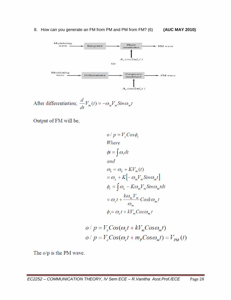
8. How can you generate an FM from PM and PM from FM? (6) (AUC MAY 2010)

EC2252 – COMMUNICATION THEORY, IV Sem ECE – R.Vanitha Asst.Prof./ECE Page 29
9. (i) A 20 MHz is frequency modulated by a sinusoidal signal such that t he maximum
frequency deviation is 100 kHz. Determine the modulation index and approximate
bandwidth of t he FM signal for t he following modulating signal frequencies, (1)1 kHz (2)
100 kHz and (3) 500 kHz. (8) (AUC MAY 2010)
Δf=100KHz
Β=?,b.w=?
1. fm=1Khz
Mf=Δf/fm=100
=2(Δf+ fm)=2025kHz
2. fm=100Khz
Mf=Δf/fm=1
=2(Δf+ fm)=400 kHz
3. fm=500Khz
=2(Δf+ fm)=1200 kHz
10. An angle modulated wave is described by the equation V (t) = 10 cos (2 £ 106¼t +10 cos
2000¼t). Find (1) Power of the modulated signal (2) Maximum frequency deviation (3)
Bandwidth. (AUC MAY 2011)
V (t) = 10 cos (2 £ 106¼t +10 cos 2000¼t).
Vc=10v,mf=10
Wc=2πfc
Fc=106Hz
Fm=1000Hz ,R=1
1. Power of the modulated signal
P total=Vc2/2R=50ohms
2. Maximum frequency deviation
Δf=mf*fm=10kHz
3. Bandwidth=2(Δf+ fm)=22kHz
11.Define frequency modulation. Draw the FM waveform. Derive an expression for single tone
frequency modulation.(2 + 2 + 6)
EC2252 – COMMUNICATION THEORY, IV Sem ECE – R.Vanitha Asst.Prof./ECE Page 30

EC2252 – COMMUNICATION THEORY, IV Sem ECE – R.Vanitha Asst.Prof./ECE Page 31

EC2252 – COMMUNICATION THEORY, IV Sem ECE – R.Vanitha Asst.Prof./ECE Page 32
(ii) Compare Narrowband and Wideband FM.(6) (AUC DEC 2011)
12. Write about the basic principle of FM detection and explain about radio detector
(AUC DEC 2011)
RATIO DETECTOR
The RATIO DETECTOR uses a double-tuned transformer to convert the instantaneous
frequency variations of the fm input signal to instantaneous amplitude variations. These
amplitude variations are then rectified to provide a dc output voltage which varies in amplitude
and polarity with the input signal frequency. This detector demodulates fm signals and
suppresses amplitude noise without the need of limiter stages.
Circuit Operation
Figure 3-12 shows a typical ratio detector. The input tank capacitor (C1) and the primary of
transformer T1 (L1) are tuned to the center frequency of the fm signal to be demodulated. The
secondary winding of T1 (L2) and capacitor C2 also form a tank circuit tuned to the center
frequency. Tertiary (third) winding L3 provides additional inductive coupling which reduces the
loading effect of the secondary on the primary circuit. Diodes CR1 and CR2 rectify the signal
from the secondary tank. Capacitor C5 and resistors R1 and R2 set the operating level of the
detector. Capacitors C3 and C4 determine the amplitude and polarity of the output. Resistor R3
limits the peak diode current and
EC2252 – COMMUNICATION THEORY, IV Sem ECE – R.Vanitha Asst.Prof./ECE Page 33
furnishes a dc return path for the rectified signal. The output of the detector is taken from the
common connection between C3 and C4. Resistor RL is the load resistor. R5, C6, and C7 form
a low-pass filter to
This circuit operates on the same principles of phase shifting as did the Foster-Seeley
discriminator. In that discussion, vector diagrams were used to illustrate the voltage amplitudes
and polarities for conditions at resonance, above resonance, and below resonance. The same
vector diagrams apply to the ratio detector but will not be discussed here. Instead, you will study
the resulting current flows and polarities on simplified schematic diagrams of the detector circuit.
OPERATION AT RESONANCE.—When the input voltage epis applied to the primary in figure
3-12 it also appears across L3 because, by inductive coupling, it is effectively connected in
parallel with the primary tank circuit. At the same time, a voltage is induced in the secondary
winding and causes current to flow around the secondary tank circuit. At resonance the tank
acts like a resistive circuit; that is, the tank current is in phase with the primary voltage ep. The
current flowing in the tank circuit causes voltages e1 and e2 to be developed in the secondary
winding of T1. These voltages are of equal magnitude and of opposite polarity with respect to
the center tap of the winding. Since the winding is inductive, the voltage drop across it is 90
degrees out of phase with the current through it. Figure 3-13 is a simplified schematic diagram
of a ratio detector at resonance. The voltage applied to
the cathode of CR1 is the vector sum of e1 and ep. Likewise, the voltage applied to the anode
of CR2 is the vector sum of e2 and ep. No phase shift occurs at resonance and both voltages
are equal. Both diodes conduct equally. This equal current flow causes the same voltage drop
across both R1 and R2. C3 and C4 will charge to equal voltages with opposite polarities. Let’s

EC2252 – COMMUNICATION THEORY, IV Sem ECE – R.Vanitha Asst.Prof./ECE Page 34
assume that the voltages across C3 and C4 are equal in amplitude (5 volts) and of opposite
polarity and the total charge across C5 is 10 volts. R1 and R2 will each have 5 volts dropped
across them because they are of equal values. The output is taken between points A and B. To
find the output voltage, you algebraically add the voltages between points A and B (loop ACB or
ADB). Point A to point D D to point B is + 5 volts. Their algebraic sum is 0 volts
and the output voltage is 0 at resonance. If the voltages on branch ACB were figured, the same
output would be found because the circuit branches are in parallel.
When the input signal reverses polarity, the secondary voltage across L2 also reverses. The
diodes will be reverse biased and no current will flow. Meanwhile, C5 retains most of its charge
because of the long time constant offered in combination with R1 and R2. This slow discharge
helps to maintain the output.
OPERATION ABOVE RESONANCE.—When a tuned circuit (figure 3-14) operates at a
frequency higher than resonance, the tank is inductive. The secondary current i lags the primary
voltage ep. Secondary voltage e1 is nearer in phase with primary voltage e, while e2 is shifted
further out of phase with ep. The vector sum of e1 and epis larger than that of e2 and ep.
Therefore, the voltage applied to the cathode of CR1 is greater than the voltage applied to the
anode of CR2 above resonance.

EC2252 – COMMUNICATION THEORY, IV Sem ECE – R.Vanitha Asst.Prof./ECE Page 35
Assume that the voltages developed above resonance are such that the higher voltage on the
cathode of CR1 causes C3 to charge to 8 volts. The lower voltage on the anode of CR2 causes
C4 to charge to 2volts. Capacitor C5 remains charged to the sum of these two voltages, 10
volts. Again, by adding the voltages in loop ACB or ADB between points A and B, you can find
the output voltage. Point A to pointDequals -2 volts. Point D to point B equals +5 volts. Their
algebraic sum, and the output, equals +3 voltswhen tuned above resonance. During the
negative half cycle of the input signal, the diodes are reverse biased and C5 helps maintain a
constant output.
OPERATION BELOW RESONANCE.—When a tuned circuit operates below resonance (figure
3-15), it is capacitive. Secondary current is leads the primary voltage epand secondary voltage
e2 is nearer in phase with primary voltage ep. The vector sum of e2 and epis larger than the
sum of e1 and ep.Thevoltage applied to the anode of CR2 becomes greater than the voltage
applied to the cathode of CR1below resonance.
Assume that the voltages developed below resonance are such that the higher voltage on the
anode of CR2 causes C4 to charge to 8 volts. The lower voltage on the cathode of CR1 causes
C3 to charge to 2volts. Capacitor C5 remains charged to the sum of these two voltages, 10
sonance.
During the negative half cycle of theinput signal, the diodes are reverse biased and C5 helps
maintain a constant output.
Advantage of a Ratio Detector
The ratio detector is not affected by amplitude variations on the fm wave. The output of the
detector adjusts itself automatically to the average amplitude of the input signal. C5 charges to
the sum of the voltages across R1 and R2 and, because of its time constant, tends to filter out
any noise impulses. BeforeC5 can charge or discharge to the higher or lower potential, the
noise disappears. The difference in chargeacross C5 is so slight that it is not discernible in the
EC2252 – COMMUNICATION THEORY, IV Sem ECE – R.Vanitha Asst.Prof./ECE Page 36
output. Ratio detectors can operate with as little as100 millivolts of input. This is much lower
than that required for limiter saturation and less gain isrequired from preceding stages.
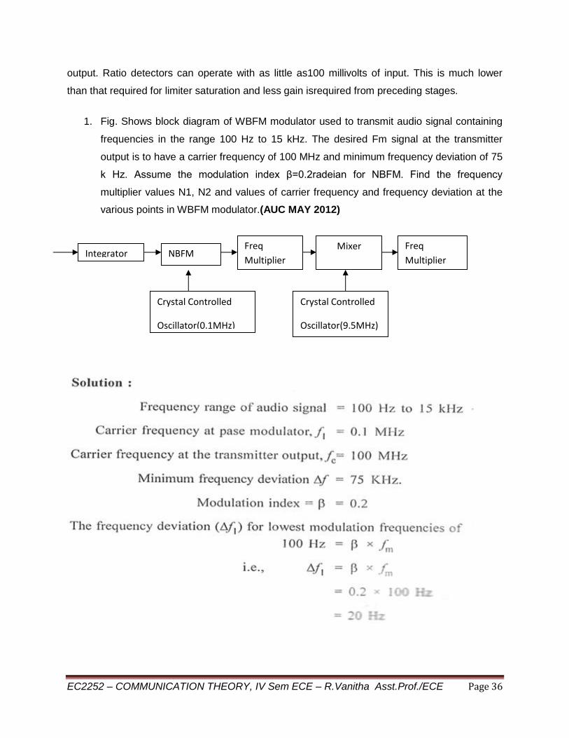
1. Fig. Shows block diagram of WBFM modulator used to transmit audio signal containing
frequencies in the range 100 Hz to 15 kHz. The desired Fm signal at the transmitter
output is to have a carrier frequency of 100 MHz and minimum frequency deviation of 75
k Hz. Assume the modulation index β=0.2radeian for NBFM. Find the frequency
multiplier values N1, N2 and values of carrier frequency and frequency deviation at the
various points in WBFM modulator.(AUC MAY 2012)
Integrator NBFM
Crystal Controlled
Oscillator(9.5MHz)
Crystal Controlled
Oscillator(0.1MHz)
Freq
Multiplier
Mixer Freq
Multiplier

EC2252 – COMMUNICATION THEORY, IV Sem ECE – R.Vanitha Asst.Prof./ECE Page 37