
Engineer-to-Engineer Note EE-394 -...
33
Engineer-to-Engineer Note EE-394 Technical notes on using Analog Devices products, processors and development tools Visit our Web resources http://www.analog.com/ee-notes and http://www.analog.com/processors or e-mail [email protected] or [email protected] for technical support. ADSP-BF70x Blackfin+ TM Processor Optimization Techniques Contributed by Li Liu Rev 1 – December 15, 2016 Copyright 2016, Analog Devices, Inc. All rights reserved. Analog Devices assumes no responsibility for customer product design or the use or application of customers’ products or for any infringements of patents or rights of others which may result from Analog Devices assistance. All trademarks and logos are property of their respective holders. Information furnished by Analog Devices applications and development tools engineers is believed to be accurate and reliable, however no responsibility is assumed by Analog Devices regarding technical accuracy and topicality of the content provided in Analog Devices Engineer-to-Engineer Notes. Introduction Analog Devices’ Blackfin+ TM processors were enhanced as compared with the previous generation Blackfin devices to provide single-cycle 32-bit multiplication or 16-bit complex math operations, dynamic branch prediction, support for misaligned data accesses, ECC/multi-parity-protected on-chip memory, and improved memory bandwidth. The Blackfin+ processors are comprised of the ADSP-BF70x products. This EE-Note describes how to optimize C/C++ applications to fully utilize these advantageous features, though most of the coding tips presented in this note are also applicable to the previous Blackfin processors as well. All of the examples in this note were implemented using an ADSP-BF707 EZ-Board® and CrossCore® Embedded Studio (CCES) 2.1.0. Please refer to Getting Started with CrossCore Embedded Studio 1.1.x (EE-372) [1] to learn how to begin development with CCES. Blackfin+ Core Overview The first step in writing efficient C/C++ code is to understand the processor on which a developer is working. This section will introduce the features of the ADSP-BF70x processor and emphasize a few that impact programming of it. First of all, Blackfin+ is a 32-bit fixed-point processor, meaning that math operations on floating-point numbers are emulated by software. In other words, the processor needs multiple cycles to complete one floating-point math operation; however, the same fixed-point math operation may only need one cycle. Similarly, 64-bit integer math operations are emulated by software. The ADSP-BF70x processor supports efficient fractional math operations (16- or 32-bit) by using the native fixed-point data types fract or accum (as defined in the stdfix.h header file) or by calling built-in functions for fractional math operations. In the latter case, fractional numbers are declared as fract16 or fract32, which are type-defined in CCES as short and int, respectively. It is important to remember that fractional numbers are different from floating-point numbers. The fractional number has a range of [-1.0, 1.0). Please refer to the Data Storage Formats section of the Compiler and Library Manual for Blackfin [2] , the Numeric Formats section of the Blackfin+ Programming Reference [3] , and the Manipulating Fractional Data section of this note for more details.
Transcript of Engineer-to-Engineer Note EE-394 -...

Engineer-to-Engineer Note EE-394
Technical notes on using Analog Devices products, processors and development tools Visit our Web resources http://www.analog.com/ee-notes and http://www.analog.com/processors or
e-mail [email protected] or [email protected] for technical support.
ADSP-BF70x Blackfin+TM Processor Optimization Techniques
Contributed by Li Liu Rev 1 – December 15, 2016
Copyright 2016, Analog Devices, Inc. All rights reserved. Analog Devices assumes no responsibility for customer product design or the use or application of
customers’ products or for any infringements of patents or rights of others which may result from Analog Devices assistance. All trademarks and logos are property of
their respective holders. Information furnished by Analog Devices applications and development tools engineers is believed to be accurate and reliable, however no
responsibility is assumed by Analog Devices regarding technical accuracy and topicality of the content provided in Analog Devices Engineer-to-Engineer Notes.
Introduction
Analog Devices’ Blackfin+TM processors were enhanced as compared with the previous generation Blackfin
devices to provide single-cycle 32-bit multiplication or 16-bit complex math operations, dynamic branch
prediction, support for misaligned data accesses, ECC/multi-parity-protected on-chip memory, and
improved memory bandwidth. The Blackfin+ processors are comprised of the ADSP-BF70x products.
This EE-Note describes how to optimize C/C++ applications to fully utilize these advantageous features,
though most of the coding tips presented in this note are also applicable to the previous Blackfin processors
as well. All of the examples in this note were implemented using an ADSP-BF707 EZ-Board® and
CrossCore® Embedded Studio (CCES) 2.1.0. Please refer to Getting Started with CrossCore Embedded
Studio 1.1.x (EE-372)[1] to learn how to begin development with CCES.
Blackfin+ Core Overview
The first step in writing efficient C/C++ code is to understand the processor on which a developer is
working. This section will introduce the features of the ADSP-BF70x processor and emphasize a few that
impact programming of it. First of all, Blackfin+ is a 32-bit fixed-point processor, meaning that math
operations on floating-point numbers are emulated by software. In other words, the processor needs multiple
cycles to complete one floating-point math operation; however, the same fixed-point math operation may
only need one cycle. Similarly, 64-bit integer math operations are emulated by software.
The ADSP-BF70x processor supports efficient fractional math operations (16- or 32-bit) by using the native
fixed-point data types fract or accum (as defined in the stdfix.h header file) or by calling built-in functions
for fractional math operations. In the latter case, fractional numbers are declared as fract16 or fract32, which
are type-defined in CCES as short and int, respectively. It is important to remember that fractional numbers
are different from floating-point numbers. The fractional number has a range of [-1.0, 1.0). Please refer to
the Data Storage Formats section of the Compiler and Library Manual for Blackfin[2], the Numeric Formats
section of the Blackfin+ Programming Reference[3], and the Manipulating Fractional Data section of this
note for more details.
ADSP-BF70x Blackfin+TM Processor Optimization Techniques (EE-394) Page 2 of 33
Enhanced Computation Capability
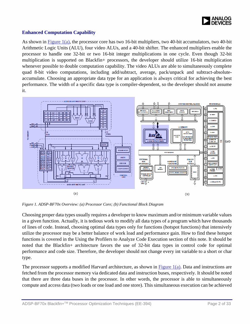
As shown in Figure 1(a), the processor core has two 16-bit multipliers, two 40-bit accumulators, two 40-bit
Arithmetic Logic Units (ALU), four video ALUs, and a 40-bit shifter. The enhanced multipliers enable the
processor to handle one 32-bit or two 16-bit integer multiplications in one cycle. Even though 32-bit
multiplication is supported on Blackfin+ processors, the developer should utilize 16-bit multiplication
whenever possible to double computation capability. The video ALUs are able to simultaneously complete
quad 8-bit video computations, including add/subtract, average, pack/unpack and subtract-absolute-
accumulate. Choosing an appropriate data type for an application is always critical for achieving the best
performance. The width of a specific data type is compiler-dependent, so the developer should not assume
it.
Figure 1. ADSP-BF70x Overview: (a) Processor Core; (b) Functional Block Diagram
Choosing proper data types usually requires a developer to know maximum and/or minimum variable values
in a given function. Actually, it is tedious work to modify all data types of a program which have thousands
of lines of code. Instead, choosing optimal data types only for functions (hotspot functions) that intensively
utilize the processor may be a better balance of work load and performance gain. How to find these hotspot
functions is covered in the Using the Profilers to Analyze Code Execution section of this note. It should be
noted that the Blackfin+ architecture favors the use of 32-bit data types in control code for optimal
performance and code size. Therefore, the developer should not change every int variable to a short or char
type.
The processor supports a modified Harvard architecture, as shown in Figure 1(a). Data and instructions are
fetched from the processor memory via dedicated data and instruction buses, respectively. It should be noted
that there are three data buses in the processor. In other words, the processor is able to simultaneously
compute and access data (two loads or one load and one store). This simultaneous execution can be achieved
ADSP-BF70x Blackfin+TM Processor Optimization Techniques (EE-394) Page 3 of 33
from C/C++ code. Following the recommendations presented in this note will significantly increase the
likelihood that the compiler generates the most efficient assembly code possible.
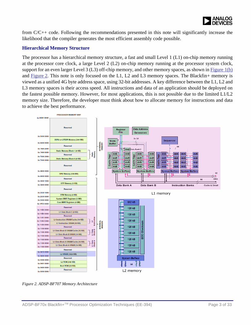
Hierarchical Memory Structure
The processor has a hierarchical memory structure, a fast and small Level 1 (L1) on-chip memory running
at the processor core clock, a large Level 2 (L2) on-chip memory running at the processor system clock,
support for an even larger Level 3 (L3) off-chip memory, and other memory spaces, as shown in Figure 1(b)
and Figure 2. This note is only focused on the L1, L2 and L3 memory spaces. The Blackfin+ memory is
viewed as a unified 4G byte address space, using 32-bit addresses. A key difference between the L1, L2 and
L3 memory spaces is their access speed. All instructions and data of an application should be deployed on
the fastest possible memory. However, for most applications, this is not possible due to the limited L1/L2
memory size. Therefore, the developer must think about how to allocate memory for instructions and data
to achieve the best performance.
Figure 2. ADSP-BF707 Memory Architecture

Copyright 2016, Analog Devices, Inc. All rights reserved. Analog Devices assumes no responsibility for customer product design or the use or application of
customers’ products or for any infringements of patents or rights of others which may result from Analog Devices assistance. All trademarks and logos are property of
their respective holders. Information furnished by Analog Devices applications and development tools engineers is believed to be accurate and reliable, however no
responsibility is assumed by Analog Devices regarding technical accuracy and topicality of the content provided in Analog Devices Engineer-to-Engineer Notes.
As manually managing L1 memory may be challenging for some developers, an alternative is to enable the
processor’s instruction and data caches. For ADSP-BF70x devices, 32 KB of L1 data memory and 16 KB
of instruction memory can be used as cache. After the caches are enabled, even if the instructions and data
of an application reside in L2/L3 memory, the processor can ultimately access a copy of them in L1 cache
at the core clock rate. This approach is also effective when an application is too complex or difficult to
distinguish hotspot functions.
The L1 and L2 memory spaces are split into several separate banks. This design is a key factor to avoid data
access conflicts. For example, if a function computes the sum of two vectors of the same length, the
application allocate the buffers to different data banks so that the processor can simultaneously access the
elements of the two vectors using different data buses.
Branch Prediction
On Blackfin+ processors, a 10-stage pipeline is used to ensure that the processor is able to execute one
instruction per cycle. However, the pipeline incurs a problem when conditional code exists (e.g., if/else,
while, for, etc.). For example, in the execution stage of the conditional code, the processor knows that it will
need the instructions of Condition A in the next cycle; however, the instructions of Condition B have been
fetched and decoded for the next cycle because these instructions are the next contiguous instructions
following the conditional code. In this case, the processor has to discard the instructions in the pipeline and
instead fetch/decode the instructions associated with Condition A, thus wasting a few precious cycles. If the
conditional code is in a loop, the performance will further degrade as the conditional code executes many
times.
To resolve this problem, the Blackfin+ processor has a dynamic branch predictor (BP) that improves the
performance of conditional code by remembering where the code vectored to the previous time it was
executed. The BP has been proven to effectively reduce a program’s execution time. For a developer,
additional actions are not required to use the BP because it has been enabled by default after coming out of
reset. Please refer to Tuning Dynamic Branch Prediction on ADSP-BF70x Blackfin+™ Processors (EE-
373)[4] for details.
Managing Processor Clocks
The core, memory and peripherals of the ADSP-BF707 processor run at different frequencies. The Dynamic
Power Management (DPM) block and the Clock Generation Unit (CGU) allow the developer to configure
the core and system frequencies. Do not assume that the processor is set to run with the highest frequency
after reset. The developer should configure the processor’s core and system frequencies to achieve the best
processor performance, especially for a custom board design. The processor core and system frequencies
can be easily managed by calling dedicated System Service and Device Driver APIs. Please refer to the
CCES On-Line Help and the System Services & Device Drivers: CrossCore® Embedded Studio on-line
training video for details.
ADSP-BF70x Blackfin+TM Processor Optimization Techniques (EE-394) Page 5 of 33
Direct Memory Access (DMA)
As mentioned, the processor has a hierarchical memory structure comprising multiple memory spaces with
different access speeds. The core is able to access data in L1 memory in one core cycle and data in L2
memory in multiple core cycles, with longer access times for L3 memory. If data are in L2/L3 memory, the
processor has to stall for multiple core cycles until the data is ready. Using cache is one way to make an
application execute efficiently. But if too many cache misses occur, the application may not achieve the
desired performance. To solve this, Direct Memory Access (DMA), can be used to allow data to be moved
between L2/L3 memory and L1 memory without core intervention.
Additionally, as was the case with core buses simultaneously accessing different banks of memory, the same
concept also holds true for the DMA channels. As the DMA engines use a dedicated bus for transfers, it
will also compete with the core for access to a targeted bank of memory. Therefore, choosing different
memory banks for receiving and sending data via DMA to remove conflicts with the core can improve the
data throughput of an application.
Trigger Routing Unit (TRU)
The Trigger Routing Unit (TRU) provides system-level event control without core intervention. The TRU
links a trigger master (the generator of an event) to a trigger slave (the receiver of the event). In this way,
the receiver can automatically respond to the sender without using a traditional interrupt, where a core is
required to pass the event to the receiver. The TRU is typically used in starting a DMA transfer when a
specific event occurs (e.g., another DMA transfer completes) or to synchronize concurrent activities.
Using the TRU, especially when an application involves an operating system, avoids the need to perform a
context switch when using traditional interrupts. The configuration of the TRU is a one-time event and is
reusable until the developer modifies the trigger masters/slaves. Please refer to Utilizing the Trigger Routing
Unit for System Level Synchronization (EE-360)[5] and the ADSP-BF70x hardware reference manual[6] for
details.
Improving Performance Using the CCES Compiler and Debug Tools
For many developers, C/C++ is the primary programming language. After coding, the compiler and its
complementary code-generation toolchain convert the source code into an executable program. Efficient
C/C++ code will make an application run faster and use less memory and power. Therefore, it is important
to use an optimizing compiler such as that provided in CCES.
Most Blackfin-based applications are currently being developed using the CCES Integrated Development
Environment (IDE), which contains tools for developing an application on an embedded platform, such as
an editor, debugger, compiler, etc. The developer should always work with the latest version of CCES for a
new project and read the compiler manual to understand the best use of the Blackfin+ compiler before
starting development. The chapter, Achieving Optimal Performance from C/C++ Source Code describes
many of the coding tips presented in this section.

ADSP-BF70x Blackfin+TM Processor Optimization Techniques (EE-394) Page 6 of 33
Using Appropriate Compiler Configurations
The first step for generating efficient assembly code is to enable optimization in the compiler. This achieves
good performance with minimum effort. To enable optimization, as shown in Figure 3, right-click the
project name in the Project Explorer window, then click Properties in the pop-up menu. Check the Enable
Optimization box in C/C++ BuildSettingsTool SettingsCrossCore Blackfin C/C++
CompilerGeneral. By default, the compiler optimizes the application for the fastest performance.
Figure 3. Enabling Compiler Optimization
For a complex application, smaller code size may be preferred versus optimal performance so that the
processor can more efficiently use the processor cache (fewer cache misses). In this case, set Optimize the
code size/speed to 0, as shown in Figure 3.
As a general principle, 80% of execution time is spent in 20% of an application’s code. Therefore, in
practice, the majority of the code should be optimized for size, whereas the hotspot functions should be
optimized for speed. To achieve this, the developer should set the project to optimize for code size in the
Project Properties but set specific source files to optimize for speed in the File Properties (right-click the
source file name instead of the project name to bring up the file-specific options). If specific functions within
a file require different optimization settings, DO NOT change the File Properties. Instead, add a pragma
before the functions that need an optimization strategy that differs from the project settings, as shown in
Listing 1. The optimize_for_speed pragma instructs the compiler to optimize the functions for maximum
speed. DO NOT forget to add #pragma optimize_as_cmd_line after the last line of the functions that need
speed optimization, otherwise the subsequent functions that are supposed to be optimized for size will be
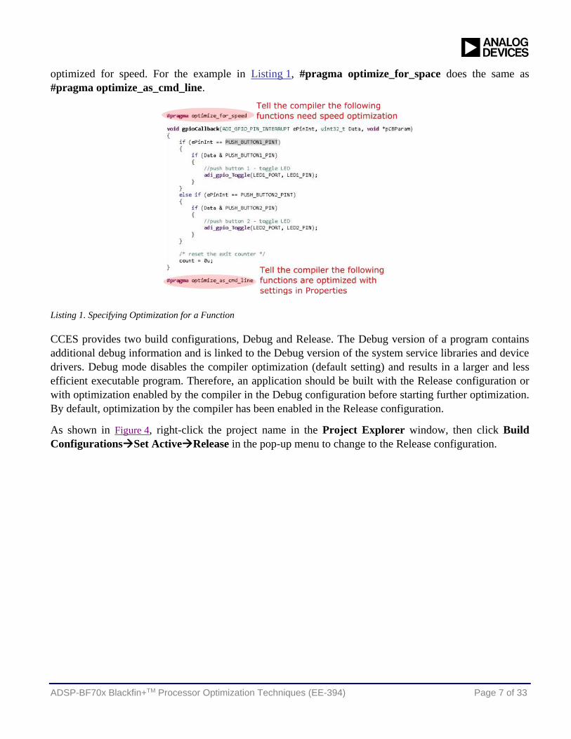
ADSP-BF70x Blackfin+TM Processor Optimization Techniques (EE-394) Page 7 of 33
optimized for speed. For the example in Listing 1, #pragma optimize_for_space does the same as
#pragma optimize_as_cmd_line.
Listing 1. Specifying Optimization for a Function
CCES provides two build configurations, Debug and Release. The Debug version of a program contains
additional debug information and is linked to the Debug version of the system service libraries and device
drivers. Debug mode disables the compiler optimization (default setting) and results in a larger and less
efficient executable program. Therefore, an application should be built with the Release configuration or
with optimization enabled by the compiler in the Debug configuration before starting further optimization.
By default, optimization by the compiler has been enabled in the Release configuration.
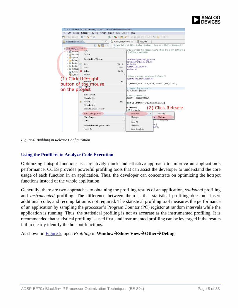
As shown in Figure 4, right-click the project name in the Project Explorer window, then click Build
ConfigurationsSet ActiveRelease in the pop-up menu to change to the Release configuration.
ADSP-BF70x Blackfin+TM Processor Optimization Techniques (EE-394) Page 8 of 33
Figure 4. Building in Release Configuration
Using the Profilers to Analyze Code Execution
Optimizing hotspot functions is a relatively quick and effective approach to improve an application’s
performance. CCES provides powerful profiling tools that can assist the developer to understand the core
usage of each function in an application. Thus, the developer can concentrate on optimizing the hotspot
functions instead of the whole application.
Generally, there are two approaches to obtaining the profiling results of an application, statistical profiling
and instrumented profiling. The difference between them is that statistical profiling does not insert
additional code, and recompilation is not required. The statistical profiling tool measures the performance
of an application by sampling the processor’s Program Counter (PC) register at random intervals while the
application is running. Thus, the statistical profiling is not as accurate as the instrumented profiling. It is
recommended that statistical profiling is used first, and instrumented profiling can be leveraged if the results
fail to clearly identify the hotspot functions.
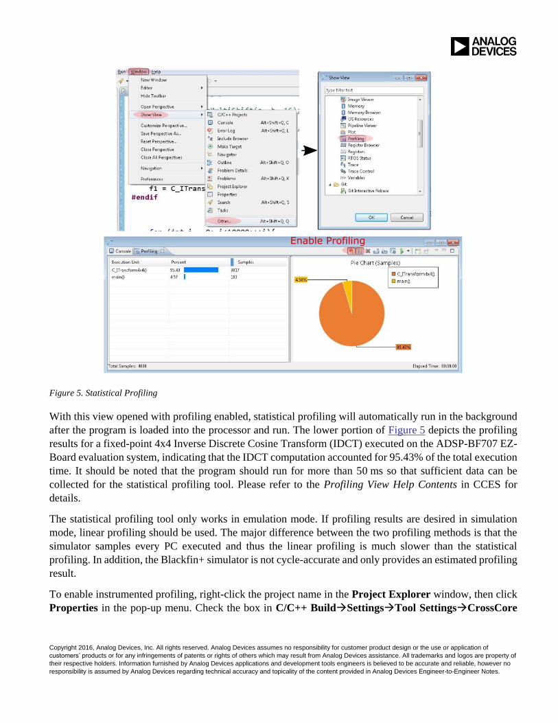
As shown in Figure 5, open Profiling in WindowShow ViewOtherDebug.
Copyright 2016, Analog Devices, Inc. All rights reserved. Analog Devices assumes no responsibility for customer product design or the use or application of
customers’ products or for any infringements of patents or rights of others which may result from Analog Devices assistance. All trademarks and logos are property of
their respective holders. Information furnished by Analog Devices applications and development tools engineers is believed to be accurate and reliable, however no
responsibility is assumed by Analog Devices regarding technical accuracy and topicality of the content provided in Analog Devices Engineer-to-Engineer Notes.
Figure 5. Statistical Profiling
With this view opened with profiling enabled, statistical profiling will automatically run in the background
after the program is loaded into the processor and run. The lower portion of Figure 5 depicts the profiling
results for a fixed-point 4x4 Inverse Discrete Cosine Transform (IDCT) executed on the ADSP-BF707 EZ-
Board evaluation system, indicating that the IDCT computation accounted for 95.43% of the total execution
time. It should be noted that the program should run for more than 50 ms so that sufficient data can be
collected for the statistical profiling tool. Please refer to the Profiling View Help Contents in CCES for
details.
The statistical profiling tool only works in emulation mode. If profiling results are desired in simulation
mode, linear profiling should be used. The major difference between the two profiling methods is that the
simulator samples every PC executed and thus the linear profiling is much slower than the statistical
profiling. In addition, the Blackfin+ simulator is not cycle-accurate and only provides an estimated profiling
result.
To enable instrumented profiling, right-click the project name in the Project Explorer window, then click
Properties in the pop-up menu. Check the box in C/C++ BuildSettingsTool SettingsCrossCore

ADSP-BF70x Blackfin+TM Processor Optimization Techniques (EE-394) Page 10 of 33
Blackfin C/C++ CompilerProcessor, as shown in Figure 6. After that, build the project and run it. In
this example, the IDCT was executed 400 times on the EZ-board evaluation system.
Figure 6. Enabling Profiling in the Compiler Configuration Settings
To create a profiling result file, click FileNewCode Analysis Report, as shown in Figure 7(a). Then,
check Instrumented Profiling, as shown in Figure 7(b). After that, select the path for the generated .prf
file (Figure 7(c)).
Figure 7. Creating the Profiling Report

ADSP-BF70x Blackfin+TM Processor Optimization Techniques (EE-394) Page 11 of 33
Figure 8 shows the instrumented profiling results.
Figure 8. Example Profiling Report
As can be seen, the IDCT accounted for 83.65% of the total execution time, and the hotspot function has
been identified. Instrumented profiling results are based on processor cycles consumed while executing the
functions. For a given function, multiple-cycle stalls incurred due to core accesses to L2/L3 memory are
accounted for in the time used by the function, even though the core is stalled. As such, the cycle count may
be bloated as a result of non-optimal memory placement as compared to the cycles required for the
computation itself, which is something that can be improved upon with strategic management of the memory
architecture when mapping code and data in the system.
Maintaining Temporary Files
In addition to the profiling tools, CCES also allows for saving of the assembly code produced by the
compiler during the project build process, which may be useful to verify if a specific function has been
optimized well by the compiler or if further hand-optimization might be possible. By default, the toolchain
discards these intermediary files, but overriding this behavior is possible via the project’s settings. Right-
click the project name in the Project Explorer window and click Properties in the pop-up menu. Check
the “Save Temporary Files” box in C/C++ BuildSettingsTool SettingsCrossCore Blackfin
C/C++ CompilerGeneral, as shown in Figure 9(a).

ADSP-BF70x Blackfin+(r) Processor Optimization Techniques (EE-394) Page 12 of 33
Figure 9. Saving Compiler-Generated Assembly Code
When the project is rebuilt with this option enabled, the generated assembly source file having the same
name as the C file but with a .s suffix, will appear in the /src folder in the debug configuration’s output
directory, as shown in Figure 9(b).
As an example where access to the intermediary assembly source file is valuable, consider a function that
computes the sum of the squared difference between two vectors, as shown in Figure 10 with the C source
at the top and the equivalent compiler-produced assembly code at the bottom:
Figure 10. C and Assembly Code for the sumsquareddiff() Function

ADSP-BF70x Blackfin+TM Processor Optimization Techniques (EE-394) Page 13 of 33
While it looks concise, the assembly code is actually not optimally efficient despite the fact that compiler
optimization is enabled. The following sections will address optimizing this example to achieve better
performance.
Helping the Compiler to Understand C/C++ Code
As mentioned previously, data types are compiler-dependent. For Blackfin+ processors, char, short and int
data types are 8-, 16-, and 32-bit, respectively. The C code in Figure 10 utilizes short and int, which can be
considered a typical implementation for this sum of squared differences routine. The corresponding
assembly code consists of four math instructions – two subtractions and two multiply-accumulates. In
practice, the result of a 16-bit multiplication is a 32-bit number. However, the assembly code uses A1:0,
two accumulators (40-bit A1 and 40-bit A0) to store the result. This is because the code implicitly uses a
32-bit multiplication, and the compiler therefore uses A1:0 (80-bit) to store a 64-bit result. In other words,
the assembly code wastes half of a valuable computing resource.
A common issue that prevents the compiler from optimizing things efficiently is that it cannot predict if an
intermediate result (such as the one from the subtraction in Figure 10) can safely inherit the operand’s data
type. If it cannot prove that such computations do not overflow, it must use the type defined by the C
standard. The subtraction result in Figure 10 will be a 32-bit number when the operands are large positive
or negative numbers. For example, for two operands, 0x6666 (26214) and 0x8001 (-32767), the result
cannot be represented by a signed 16-bit integer.
A quick way to make the compiler aware of the fact that the math operations are 16-bit is to add a temporary
16-bit variable to store the intermediate subtraction result to, as shown in Figure 11.
Figure 11. Optimized C/ASM Code for the Example
Consequently, as can be seen in the generated assembly source, the math operations are 16-bit, and the
compiler can issue two 16-bit multiplications in parallel.
ADSP-BF70x Blackfin+TM Processor Optimization Techniques (EE-394) Page 14 of 33
The purpose of this example is to remind the developer of the importance of carrying out three suggestions
while writing/optimizing C code:
1. Know the maximum or minimum values of variables.
2. Choose appropriate data types for variables.
3. Examine the generated assembly code during optimization.
Native Fixed-Point Types
As mentioned in the Introduction, Blackfin+ processors support fractional numbers, which are not defined
in standard C. Thus, in practice, fractional numbers are often stored as short (16-bit) or int (32-bit) data
type. However, a better technique for functions that involve fractional numbers is to use the native fixed-
point types supported by the compiler so that the compiler can better understand C code and has a better
chance of generating more efficient assembly code. Refer to the Compiler Manual for details about
fractional numbers.
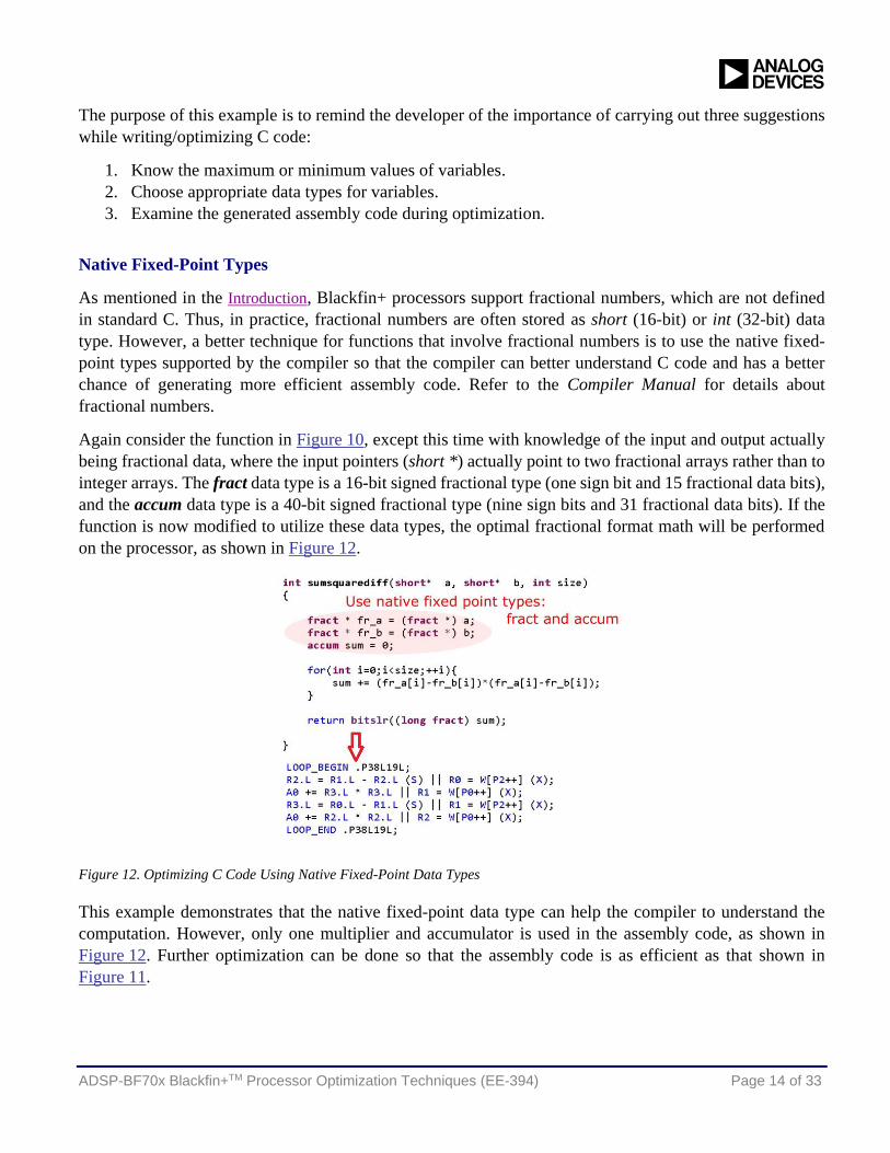
Again consider the function in Figure 10, except this time with knowledge of the input and output actually
being fractional data, where the input pointers (short *) actually point to two fractional arrays rather than to
integer arrays. The fract data type is a 16-bit signed fractional type (one sign bit and 15 fractional data bits),
and the accum data type is a 40-bit signed fractional type (nine sign bits and 31 fractional data bits). If the
function is now modified to utilize these data types, the optimal fractional format math will be performed
on the processor, as shown in Figure 12.
Figure 12. Optimizing C Code Using Native Fixed-Point Data Types
This example demonstrates that the native fixed-point data type can help the compiler to understand the
computation. However, only one multiplier and accumulator is used in the assembly code, as shown in
Figure 12. Further optimization can be done so that the assembly code is as efficient as that shown in
Figure 11.

ADSP-BF70x Blackfin+TM Processor Optimization Techniques (EE-394) Page 15 of 33
Vectorizing the Accumulation
The compiler usually does not vectorize fractional accumulations unless it is told that simultaneously using
two accumulators is safe. In other words, only using the native fixed-point types may not generate the best
assembly code. To vectorize the accumulators, saturating arithmetic (as used in fractional arithmetic) should
specifically be allowed to be reordered. This is selectable in the compiler settings by selecting the
Additional Options page of the C/C++ BuildSettingsTool SettingsCrossCore Blackfin C/C++
Compiler tree under the project properties page and keying in “-sat-associative”, as shown in Figure 13.
Figure 13. Adding Compiler Option to Vectorize the Accumulators
When the project is subsequently rebuilt, the assembly code is updated, as shown in Listing 2.
Listing 2. Optimized Assembly Code with -sat-associative Option Enabled
Note that the code in Listing 2 is not exactly the same as that in Figure 11, as the assembly instruction utilize
different instruction modifiers (suffixes), which have different meanings in the computation. Please refer to
the Instruction Set Reference pages in the Blackfin+ Programming Reference for details.
Impact of Assembly Instruction Suffixes
For Blackfin+ processors, a fractional number and a short integer, which have the same number of bits,
represent totally different values. For example, 0x1000 (16-bit) is 4096 (integer) or 0.125 (fractional). The
compiler generates assembly code based on the data types of variables and utilizes instruction suffixes to
differentiate operands’ data types. Thus, the same instruction with different suffixes yields different results.
As a comparison, the multiply-accumulate operation in Figure 11 is identical to that of the same compiler-
generated code of Listing 2 except for the suffix, as highlighted in Figure 14.

ADSP-BF70x Blackfin+TM Processor Optimization Techniques (EE-394) Page 16 of 33
Figure 14. Comparing ASM Instructions Produced By Compiler
The (IS) suffix indicates that the operands are signed integers. The difference between these two assembly
instructions is that the instruction without the suffix is multiplying two fractional numbers, which means
that the unscaled result will be in the format 2.30 (with two sign bits and 30 fractional data bits). As such,
the 1.31 fractional format output is left-shifted by one bit, thus doubling the result. This behavior lends itself
to a trick for a specific integer math operation where a multiplication is followed by a 1-bit left shift, such
as the code in Figure 15.
Figure 15. C and Assembly Code for Multiplication Followed by 1-bit Left Shift
As can be seen, the compiler automatically optimizes the C code to a single assembly instruction.
Using Built-In Functions
The compiler includes a set of built-in functions that facilitate the generation of efficient code. For example,
there is a built-in function associated with the multiply-accumulate used in Figure 11 called mult_fr1x32(),
as shown in Figure 16:

ADSP-BF70x Blackfin+TM Processor Optimization Techniques (EE-394) Page 17 of 33
Figure 16. Using Compiler Built-In Functions
As can be seen, the compiler-produced assembly code is fully optimized, as expected. Refer to the compiler
manual for details regarding all the supported built-in functions.
Built-in functions are compiler-dependent and are not portable to other platforms.
Using the Optimized DSP Run-Time Library
A number of DSP functions have been implemented and optimized for Blackfin+ processors. Before
developing an algorithm, it is good practice to first search the CCES tools installation to determine if the
basic functions of the algorithm have been included in the DSP run-time library. Using the optimized DSP
run-time functions will save lots of development time and avoid the need for time-consuming optimization.
Functions contained in the DSP run-time library include Fast Fourier Transforms, Finite/Infinite
Impulse Filters, Matrix computations, Convolution, Statistics, etc. Refer to the compiler manual for more
details.
Improve Iteration Efficiency
A common feature of many hotspot functions is that they contain loops that are iterated numerous times.
An insignificant improvement for a single loop iteration may accumulate to become a significant
opportunity for performance improvement when the iteration is executed many times. For example, if
conditional code exists in the iteration, the performance improvement resulting from such an optimization
may be more significant when considering the number of times the code is executed. Thus, conditional code
should be avoided in loop bodies, especially in inner loops.
Blackfin+ processors support two levels of zero-overhead hardware loops. This feature is utilized when the
number of iterations for a loop – or “trip count” – can be computed before the loop starts. Otherwise, the
compiler utilizes “jump” instructions to implement the loop.
ADSP-BF70x Blackfin+TM Processor Optimization Techniques (EE-394) Page 18 of 33
The C code in Figure 11 is applicable for any number of loop iterations. If the trip count is a known value
or in a range, specifying it in the C code will enable the compiler to make more reliable decisions about the
optimization strategy for the loop, such as allowing the loop to be partially unrolled or vectorized. A set of
pragmas can be used to provide the compiler with more information about a loop (refer to the compiler
manual for details). Some of the relevant pragmas are:
#pragma loop_count(min, max, modulo) – informs the compiler of the minimum and maximum
trip counts of the loop, as well as a number known to exactly divide the trip count
#pragma different_banks – informs the compiler that parallel accesses can occur concurrently
because data is in different memory banks
#pragma no_alias – informs the compiler that no load or store operation within the body of the loop
accesses the same memory
In most cases where a C function calls another function, a few lines of assembly code are required and are
inserted to store values in scratch registers before entering a sub-function and to restore the registers’ values
after returning from the sub-function. This means that extra cycles are needed to complete the required
context switch, which means that calling sub-functions inside a loop will somewhat degrade performance.
As such, the compiler will try to avoid generating a hardware loop if the loop body contains a function call.
Therefore, it will improve performance to expand small functions within loop bodies whenever possible or
to use the “inline” qualifier to tell the compiler to try to inline those functions.
Using the volatile ANSI C Extension
During optimization, the compiler assumes that variables’ values are not changed unless they are explicitly
modified in the code. This means that values can be loaded from memory in advance and reused if they are
known to be static between uses. However, for variables storing data from the peripherals, values in memory
may be written in a way that is not detectable by the compiler. Writes to such variables may also occur in
interrupt handlers, which again cannot be seen by the compiler’s optimizer. To avoid the compiler using
stale values, the volatile ANSI C extension must be used when declaring such implicitly-modified variables.
The same is true for variables such as loop counters, which can be initialized in the loop’s construct and not
modified anywhere other than in the loop definition. As the counter is not used nor modified anywhere else,
the optimizer can remove it unless instructed not to by the volatile extension. This concept, as well as several
other common issues occurring when optimization is enabled, is discussed in the FAQ entitled “Why does
my code stop working when I enable optimization?”[9] in Analog Devices’ Engineer Zone.
Avoid Division
Division on Blackfin+ processors is emulated by software and takes multiple cycles to complete (>12).
Thus, division operations should be avoided whenever possible. For binary divisors (2, 4, 8, …, 231), the
compiler replaces the division with a single-cycle shift operation. It may also replace a division by a
sequence of multiplications when the divisor is a known value.

ADSP-BF70x Blackfin+TM Processor Optimization Techniques (EE-394) Page 19 of 33
Optimizing an Application Using Blackfin+ Assembly Code
Writing assembly language should be considered to be the last resort when optimizing an application. This
technique is not recommended unless the compiler does not generate efficient enough assembly code after
the above optimization approaches have been applied. In most cases, only a small proportion of application
functions might benefit by being written in assembly code. Although this note does not cover algorithm
optimization, this should be performed prior to trying to write assembly code.
In general, there are two approaches to using assembly language in an application, either indirectly writing
assembly-like code in a C/C++ source file or directly writing assembly code in a dedicated assembly source
file. This note will only cover the former, as the latter requires a deeper understanding of Blackfin+
programming skills.
The asm() ANSI C extension allows assembly instructions to be dropped in situ into the compiler’s output
from within the structure of an otherwise fully C/C++ source file. Although this technique is easier than
directly writing a full module in assembly code, it is important to take care to avoid creating bugs at the
assembly level or within the C run-time environment, as the compiler is largely unaware of the text being
inserted inside the asm() construct. If the text inside the construct contains a syntax error, it will be flagged
as such when parsed by the assembler during the project build. However, concepts such as register
utilization, data type matching, and the C/Assembly interface must be considered when creating this code,
as the compiler is unaware of how this assembly code will behave when inserted into the compiler-generated
assembly code output.
For example, the code in Figure 17 calculates the sum of two integers.
Figure 17. Example asm() Construct
Although the variables a, b and r are declared as short int (16-bit data), the asm() construct specifies the
registers as 32-bit by using the d designator (directing the compiler to use a data register). Thus, variables
a and b occupy the whole 32-bit data registers R2 and R3 (pink ellipses). In contrast, the compiler correctly
understands the C code and utilizes only the lower 16-bit halves of the data registers (blue ellipses).
To correct this issue, the asm() construct should be written as asm("%0 = %1 +%2;":
"=H"(r):"H"(a),"H"(b));. The “H” asks the compiler to only use the lower/higher 16-bit half of a data
register rather than the whole 32-bit register. Please refer to the CCES On-Line Help Inline Assembly
Language Support Keyword (asm) topic for details about the asm() ANSI C extension syntax.

ADSP-BF70x Blackfin+TM Processor Optimization Techniques (EE-394) Page 20 of 33
Memory Optimization
To obtain a highly efficient program, optimizing algorithms/code is only a portion of the effort. Utilizing
placement of data/instructions in memory to take full advantage of the architecture also plays an important
role in improving overall application performance. As covered previously, the profiling tool should be used
to identify hotspot functions before starting memory optimization. If the compiler-generated assembly code
for those functions has been optimized to the extent where additional efforts will only gain marginal
improvement, it is time to consider optimizing the system memory map for the application. The primary
principle of memory optimization is to allocate memory for instructions and data based on their importance.
The most frequently executed instructions and accessed data should be loaded into L1 memory wherever
possible. If there is not enough space in L1 memory, L2 memory should be used next, followed lastly by
L3 memory.
Cache Management
ADSP-BF707 processors have a 64 KB region of memory for each of data and instructions, plus an 8 KB
scratchpad memory for data, as shown in Figure 2. 32KB of data memory and 16 KB of instruction
memory can be configured as cache. For a complex application, enabling both of these caches should
significantly improve its performance.
The cache can be configured in CCES by double-clicking the System Configuration (system.svc) file in
the Project Explorer. If the Startup Code/LDF tab at the bottom of the window is active, the cache
settings are accessible via the Cache Configuration tab on the left, as shown in Figure 18.
Figure 18. Enabling Cache in CCES
In most cases, the cache should be configured as depicted in Figure 18 (i.e., Enable instruction cache and
Enable data cache on banks A and B), though it is fully customizable to allow for enabling of only
instruction cache or only data cache (either both banks or just bank A).

ADSP-BF70x Blackfin+TM Processor Optimization Techniques (EE-394) Page 21 of 33
The small cache mapping size (16 KB) is preferred for most applications because a smaller mapping size
usually makes the cache work more efficiently when the size of a data block is not large. In contrast, the
larger cache mapping size will make the cache work more efficiently when the size is fairly large (e.g., >
8 MB).
The write-back mode is preferred from a system bandwidth standpoint because the write action back to the
source memory only occurs when new cache line fill replaces a cache line containing modified data, whereas
the alternative write-through cache mode causes the writes to the source memory to occur immediately
whenever data in the cache line is overwritten, which causes extra accesses to the slower external L3
memory. While better in terms of system performance, using write-back mode may lead to issues with cache
coherency. For example, if a transmit DMA sources a cacheable buffer in L3 memory, the data sent may be
stale if the core has updated the data in the cache and a write-back operation hasn’t been required due to
cache thrashing.
A quick solution to this cache coherency issue is to call the flush_data_cache()
built-in function to force the core to write the modified data back to the source
memory before a DMA transfer starts.
Using the CCES Linker for Placement of Application Data
When a new project is created, CCES adds a Startup/LDF file into it. The linker extracts code and data input
sections by name from the project’s various object (DOJ) files and maps them to defined memory segments
in the system memory map using the memory model declared in the Linker Description File (LDF). If all
the input sections get successfully resolved to the defined memory spaces, the output of the linker is the
executable (DXE) file that runs on the processor. If any portion of an input section is unresolved after all
defined system memory has been exhausted, a linker error is generated. Thus, part of the memory
optimization process is to understand how the linker works and modify the LDF file (and possibly also the
source code) to make the most effective use of the memory architecture.
The compiler generates input section information that the linker must then interpret in order to place the
application appropriately in memory, which is governed in the project’s LDF file, the relevant portions of
which are shown in Figure 19.

ADSP-BF70x Blackfin+(r) Processor Optimization Techniques (EE-394) Page 22 of 33
Figure 19. Example LDF
The memory segments (e.g. MEM_L1_DATA_C, MEM_L1_CODE, etc.) are defined at the top with a type,
address range, and width. A little further down in the LDF is where the mapping takes place, initiated by
the INPUT_SECTIONS command, where the input section names are provided as arguments directing the
linker to look for these input sections in the input object files listed and try to map all data or code associated
with that input section to the memory segment being populated. The example shown is highlighting the fact
that there are several default input section names available, a generic L1_data input section that is mapped
to both data memory banks A and B, as well as unique input section names for each of data banks A and B
– L1_data_a and L1_data_b, respectively.
Although the processor has a unified memory address space, L1/L2 memory is divided into several memory
blocks, each of which has dedicated ports connecting to the data bus (Figure 2). Referring again to the code
in Figure 15, if the a and b arrays are allocated to the same memory block, a data access conflict will prevent
the processor from executing the assembly instruction (multiplication and loading) in a single cycle, even
though the C code has been fully optimized. If the application data is not explicitly mapped, the linker will
utilize memory based on the default LDF.
To take a look at how the linker is resolving the application, a memory usage report (called a MAP file) can
be generated for all the functions in the application, as well as for all global and static local data. To generate
the MAP file, access the Project Properties and check the Generate symbol map box on the C/C++

ADSP-BF70x Blackfin+TM Processor Optimization Techniques (EE-394) Page 23 of 33
BuildSettingsTool SettingsCrossCore Blackfin C/C++ LinkerGeneral page, as shown in the
left window of Figure 20.
Figure 20. Enabling Generation of the Symbol Map
The generated XML file having a name format of ProjectName.map.xml will be found in the active debug
configuration’s output directory when the project is subsequently built, as shown in the right window in
Figure 20.
Non-static local variables are not included in the report, as they are dynamically
allocated on the system stack during application execution.
The resulting report contains an overall memory map broken down into the output memory segment names
defined in the LDF, along with their defined type/range/width and an indication of how much of the memory
is being consumed by the application, as shown in Figure 21.

ADSP-BF70x Blackfin+(r) Processor Optimization Techniques (EE-394) Page 24 of 33
Figure 21. Example Symbol Map
Beneath this overall map of the memory segments is a breakdown by input object file (.doj files) as to the
section names (e.g., data1, L1_data_a, and L1_data_b) that are being mapped to the various memory
segments (e.g., MEM_L1_DATA_A/B/C, etc.). These tables flesh out the mapped symbols along with their
size in bytes and location. As can be seen in the lower left portion of Figure 21, the linker’s default behavior
is to assign the arrays, a (at address 0x11b00648) and b (at address 0x11b00668), to the same block because
the compiler by default associates global data with the input section name data1. The default LDF maps the
data1 input section to all of the memory regions defined, and the linker will parse the LDF from top-to-
bottom and from left-to-right in terms of the order in which it will attempt to place things in memory.
In the above case, the two arrays are declared contiguously in the code, and when the linker made the pass
to map everything from the myOptimizationExample.doj object file, it was filling the MEM_L1_DATA_C
memory segment, and both arrays fit in the space available within it, so both arrays were mapped
contiguously within that segment. Had array b been too large to fit in this memory segment, the linker would
have temporarily placed it aside, parsed any remaining object files for the data1 input section, and attempted
to map that data to the MEM_L1_DATA_C segment until all of the input sections for MEM_L1_DATA_C
were completed. Once the MEM_L1_DATA_C segment was fully processed, the linker would have moved
on to the next memory segment and would again have tried to map the unresolved b array in the data1 input
section if the data1 input section were defined to be a valid input section for that memory segment.
Since the two arrays are in the same bank, extra cycles will be implicitly incurred due to access conflicts
when the data are loaded concurrently by parallel loads in a multi-issue assembly instruction. To rectify this
behavior, the linker can be directed to put the two arrays into unique memory blocks by adding #pragma
section (“L1_data_a”) and (“L1_data_b”) where the arrays are declared in the source code, as shown in
Listing 3.

ADSP-BF70x Blackfin+TM Processor Optimization Techniques (EE-394) Page 25 of 33
Listing 3. Assigning Data to Different Memory Banks
This pragma takes advantage of the alternative input section names defined in the default LDFs that are
unique to each of data banks A and B, respectively, though it is also used when the input sections are defined
by the user. When the project is subsequently rebuilt after adding these pragma statements, the output MAP
file reflects the optimized memory assignment, as highlighted in the lower right of Figure 21, where the a
and b arrays have been assigned to different blocks, MEM_L1_DATA_A (at address 0x11800000) and
MEM_L1_DATA_B (at address 0x11900000), respectively.
It should be noted that the default LDF does not specifically distinguish between the different memory sub-
blocks within the 32 KB data banks A nor B, which could be exploited to take maximal advantage of the
architecture. If the application could benefit from finer control among the sub-blocks within the bank,
further manual modifications to the LDF are necessary. For example, if the application required data bank
A to be broken down into three smaller banks, one that is 16 KB (MEM_L1_DATA_A) and two that are
8 KB each (MEM_L1_DATA_A1 and MEM_L1_DATA_A2), the memory boundaries would need to be
redefined in the memory section of the LDF, as shown in Figure 22.
Figure 22. Modifying the LDF to Define Sub-Banks in Memory

ADSP-BF70x Blackfin+TM Processor Optimization Techniques (EE-394) Page 26 of 33
Also highlighted in Figure 22 is the fact that custom input section names, “L1_data_a1” and “L1_data_a2”,
are being defined and assigned in the mapping commands for the newly created MEM_L1_DATA_A1 and
MEM_L1_DATA_A2 memory segments, respectively.
The other identifiers (e.g., L1_data, etc.) should be preserved and included
in the mapping command so that any remaining unused memory in
MEM_L1_DATA_A1 and MEM_L1_DATA_A2 can be filled by data
associated with the default input section names.
By using the modified LDF with the “L1_data_a1” and “L1_data_a2” input section names, in conjunction
with adding the pragma statements to the source code that identify these section names, the a and b arrays
get resolved to two sub-banks inside of data bank A, as shown in Figure 23.
Figure 23. New Memory Map with Data Bank A Partitioned into Sub-Banks
In addition to the above, the function in Figure 15 can be modified to add the previously mentioned
#pragma different_banks, as shown in Figure 24.
Figure 24. Adding the different_banks Pragma to the Code
As described, this added pragma ensures that the compiler can see that the a and b arrays are located in
different memory blocks, thus meaning that they can be loaded in parallel without risk of access conflicts.

ADSP-BF70x Blackfin+TM Processor Optimization Techniques (EE-394) Page 27 of 33
Stack and Heap Memory Management
Among the data that must be managed are the stack and heap for the application. The stack is used for
monitoring program flow, storing local variables in a function, argument passing, and storing register
contents for a context switch. The heap is used for runtime memory allocation for variables whose size is
often unknown at compilation and in association with dynamic memory allocation protocols such as
malloc(), calloc(), free(), etc.
By default, the LDF allocates 2 KB of memory for each of these, but this size may not be appropriate for a
given application and is configurable via the LDF tab on the Startup Code/LDF tab at the bottom of the
System Configuration Utility (system.svc), as shown in Figure 25.
Figure 25. Stack and Heap Memory Configuration
As shown, 8 KB of L1 internal memory is being allocated for the system stack, and 16 KB of L2 internal
memory is being allocated for the system heap, but these sizes can be customized based on the application’s
requirements.
Typically, the stack is located in L1 memory so that the processor doesn’t incur access penalties when
executing context switches for a subroutine or interrupt handler. For an application, it is critical to allocate
sufficient memory space for an application’s stack, otherwise the application can crash during execution.
For example, if a recursive function needs a 1 KB temporary array, the application will crash due to
insufficient stack memory when recursively executed eight times.
The heap, on the other hand, is usually allocated to L2/L3 memory. As mentioned previously, the core will
stall when directly accessing data in L2/L3 memory; thus, using cache or DMA is a common approach when
accessing heap data.
ADSP-BF70x Blackfin+TM Processor Optimization Techniques (EE-394) Page 28 of 33
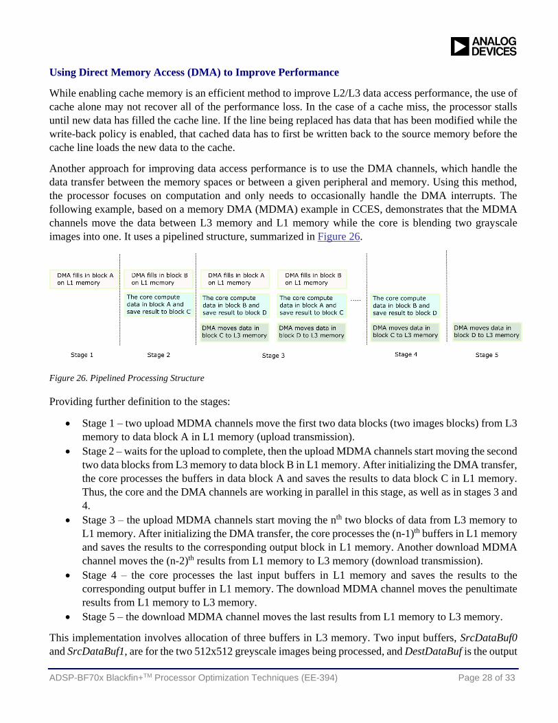
Using Direct Memory Access (DMA) to Improve Performance
While enabling cache memory is an efficient method to improve L2/L3 data access performance, the use of
cache alone may not recover all of the performance loss. In the case of a cache miss, the processor stalls
until new data has filled the cache line. If the line being replaced has data that has been modified while the
write-back policy is enabled, that cached data has to first be written back to the source memory before the
cache line loads the new data to the cache.
Another approach for improving data access performance is to use the DMA channels, which handle the
data transfer between the memory spaces or between a given peripheral and memory. Using this method,
the processor focuses on computation and only needs to occasionally handle the DMA interrupts. The
following example, based on a memory DMA (MDMA) example in CCES, demonstrates that the MDMA
channels move the data between L3 memory and L1 memory while the core is blending two grayscale
images into one. It uses a pipelined structure, summarized in Figure 26.
Figure 26. Pipelined Processing Structure
Providing further definition to the stages:
Stage 1 – two upload MDMA channels move the first two data blocks (two images blocks) from L3
memory to data block A in L1 memory (upload transmission).
Stage 2 – waits for the upload to complete, then the upload MDMA channels start moving the second
two data blocks from L3 memory to data block B in L1 memory. After initializing the DMA transfer,
the core processes the buffers in data block A and saves the results to data block C in L1 memory.
Thus, the core and the DMA channels are working in parallel in this stage, as well as in stages 3 and
4.
Stage 3 – the upload MDMA channels start moving the nth two blocks of data from L3 memory to
L1 memory. After initializing the DMA transfer, the core processes the (n-1)th buffers in L1 memory
and saves the results to the corresponding output block in L1 memory. Another download MDMA
channel moves the (n-2)th results from L1 memory to L3 memory (download transmission).
Stage 4 – the core processes the last input buffers in L1 memory and saves the results to the
corresponding output buffer in L1 memory. The download MDMA channel moves the penultimate
results from L1 memory to L3 memory.
Stage 5 – the download MDMA channel moves the last results from L1 memory to L3 memory.
This implementation involves allocation of three buffers in L3 memory. Two input buffers, SrcDataBuf0
and SrcDataBuf1, are for the two 512x512 greyscale images being processed, and DestDataBuf is the output
ADSP-BF70x Blackfin+TM Processor Optimization Techniques (EE-394) Page 29 of 33
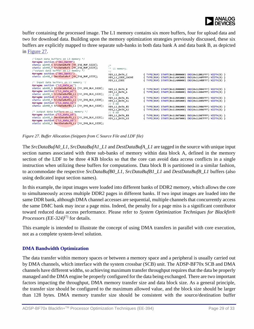
buffer containing the processed image. The L1 memory contains six more buffers, four for upload data and
two for download data. Building upon the memory optimization strategies previously discussed, these six
buffers are explicitly mapped to three separate sub-banks in both data bank A and data bank B, as depicted
in Figure 27.
Figure 27. Buffer Allocation (Snippets from C Source File and LDF file)
The SrcDataBufA0_L1, SrcDataBufA1_L1 and DestDataBufA_L1 are tagged in the source with unique input
section names associated with three sub-banks of memory within data block A, defined in the memory
section of the LDF to be three 4 KB blocks so that the core can avoid data access conflicts in a single
instruction when utilizing these buffers for computations. Data block B is partitioned in a similar fashion,
to accommodate the respective SrcDataBufB0_L1, SrcDataBufB1_L1 and DestDataBufB_L1 buffers (also
using dedicated input section names).
In this example, the input images were loaded into different banks of DDR2 memory, which allows the core
to simultaneously access multiple DDR2 pages in different banks. If two input images are loaded into the
same DDR bank, although DMA channel accesses are sequential, multiple channels that concurrently access
the same DMC bank may incur a page miss. Indeed, the penalty for a page miss is a significant contributor
toward reduced data access performance. Please refer to System Optimization Techniques for Blackfin®
Processors (EE-324)[7] for details.
This example is intended to illustrate the concept of using DMA transfers in parallel with core execution,
not as a complete system-level solution.
DMA Bandwidth Optimization
The data transfer within memory spaces or between a memory space and a peripheral is usually carried out
by DMA channels, which interface with the system crossbar (SCB) unit. The ADSP-BF70x SCB and DMA
channels have different widths, so achieving maximum transfer throughput requires that the data be properly
managed and the DMA engine be properly configured for the data being exchanged. There are two important
factors impacting the throughput, DMA memory transfer size and data block size. As a general principle,
the transfer size should be configured to the maximum allowed value, and the block size should be larger
than 128 bytes. DMA memory transfer size should be consistent with the source/destination buffer

ADSP-BF70x Blackfin+TM Processor Optimization Techniques (EE-394) Page 30 of 33
alignment in memory, otherwise an Address Alignment Error will occur during data transfer. The alignment
of the start address of the buffer must be a multiple of 2, 4, 8, or 16 bytes if the transfer size is set to 2, 4, 8,
or 16 bytes (respectively).
Another important factor that determines DMA bandwidth is the priority scheme for concurrent DMA
channels, which establishes which channel gains access to the bus. While the processor has a default priority
defined for all DMA channels, it is configurable so that important DMA channels can be assigned higher
priority, per the application’s requirements. Please refer to ADSP-BF70x Blackfin+™ Processor System
Optimization Techniques (EE-376)[8] for details.
Manipulating Fractional Data
The fractional numbers supported by Blackfin+ processors range from [-1.0,1.0), though this range may not
be sufficient. In practice, the range can be somewhat extended with the trade-off being some degree of loss
of fractional precision. For example, the least significant bit of a 1.15 (one sign bit and 15 fractional data
bits) fractional number represents 2-15, whereas the least significant bit of a 3.13 fractional number only
represents 2-13. The 16-bit hex number 0x3C0F represents 0.469208 when treated as a 1.15 fractional
number. This very same value interpreted as a 3.13 number is 1.219208, and it is up to the application as to
how to interpret the hex value. From the perspective of the Blackfin+ processor, 0x3C0F is either a 1.15
fractional number or a 16.0 integer when performing computations. This section will illustrate the
manipulation of fractional data by implementing a 16-bit positive integer base-10 logarithm.
The logarithm function provided by the DSP runtime library is designed for floating-point numbers and is
emulated by software. If the logarithm is to be performed on an integer, the integer must first be cast as a
floating-point number, and the result is also a floating-point number. The issue here is that the software-
emulated floating-point logarithm takes many cycles for one calculation and may result in a bottleneck for
some applications that require thousands of logarithm operations. If an application only needs a positive
integer logarithm, an alternative approach is to create an offline lookup table containing pre-calculated log
values, and then perform online interpolation to do the logarithm. This section uses 16-bit unsigned integers
as an example.
Any positive integer can be viewed as a combination of a high byte and a low byte. The high byte can be
used as an index into the pre-calculated log value look-up table, and then the low byte can be used with the
obtained log value to compute the true log value by using an interpolative approach. This method actually
divides integers into multiple groups, each consisting of 256 integers. For small integers, the groups can be
iteratively sub-divided into smaller groups until an acceptable precision is reached. Listing 4 shows python
code that is one example that of how to create the look-up table.
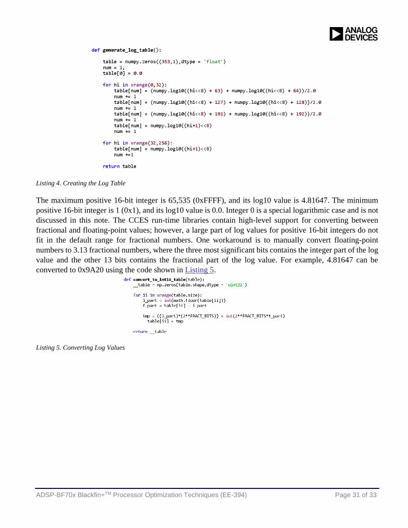
ADSP-BF70x Blackfin+TM Processor Optimization Techniques (EE-394) Page 31 of 33
Listing 4. Creating the Log Table
The maximum positive 16-bit integer is 65,535 (0xFFFF), and its log10 value is 4.81647. The minimum
positive 16-bit integer is 1 (0x1), and its log10 value is 0.0. Integer 0 is a special logarithmic case and is not
discussed in this note. The CCES run-time libraries contain high-level support for converting between
fractional and floating-point values; however, a large part of log values for positive 16-bit integers do not
fit in the default range for fractional numbers. One workaround is to manually convert floating-point
numbers to 3.13 fractional numbers, where the three most significant bits contains the integer part of the log
value and the other 13 bits contains the fractional part of the log value. For example, 4.81647 can be
converted to 0x9A20 using the code shown in Listing 5.
Listing 5. Converting Log Values

ADSP-BF70x Blackfin+TM Processor Optimization Techniques (EE-394) Page 32 of 33
The integer logarithm on Blackfin+ is implemented with linear Newton’s method, as shown in Listing 6.
Listing 6. Calculating Log Values with Interpolation
As discussed, the same hex number can be interpreted as different values when considered as a 2.14, 3.13,
or 4.12 fractional number. However, for Blackfin+ processors, there is no difference in computation because
the hex number itself never changes. For example, using the following look-up function, the log value of
the decimal number 6421 (0x1915) comes out to 0x79D7, which represents 3.807495. This result is quite
close to the log10 value calculated using Matlab (3.807603).
Summary
A key factor in optimization is to understand the capabilities of the compiler and processor. Following the
recommendations presented in this EE-note will increase the potential for achieving efficient assembly code
and improved system performance. The optimization process can be summarized in several steps and is an
iterative process that may need to be repeated until desired application performance is reached:
1. Run the profiling tool to locate hotspot functions.
2. Analyze root causes that degrade the functions’ performance.
a. If the root cause is inefficient memory access:
i. Enable processor cache (instruction and data).
ii. Optimize data memory placement in the LDF.
iii. Utilize DMA to move data between L1 memory and the L2/L3 memory spaces.
b. If the root cause is inefficient assembly code:
i. Enable the compiler optimizer.
ii. Optimize algorithms using built-in functions or DSP library functions.
iii. Optimize instruction memory usage in the LDF.
iv. Refine the data types.
v. Optimize loop bodies in the hotspot functions.
ADSP-BF70x Blackfin+TM Processor Optimization Techniques (EE-394) Page 33 of 33
3. Check whether the desired performance has been reached, and repeat the above sequence until the
desired performance goals have been achieved.
References
[1] Getting Started with CrossCore® Embedded Studio 1.1.x (EE-372). Rev 1, March 2015. Analog Devices, Inc.
[2] CrossCore® Embedded Studio 2.2.0 C/C++ Compiler and Library Manual for Blackfin Processors. Rev 1.6, February
2016. Analog Devices, Inc.
[3] ADSP-BF70x Blackfin+® Processor Programming Reference. Rev 0.2, May 2014. Analog Devices, Inc.
[4] Tuning Dynamic Branch Prediction on ADSP-BF70x Blackfin+® Processors (EE-373). Rev 1, July 2015. Analog
Devices, Inc.
[5] Utilizing the Trigger Routing Unit for System Level Synchronization (EE-360). Rev 1, October 2013. Analog Devices, Inc.
[6] ADSP-BF70x Blackfin+® Processor Hardware Reference. Rev 0.2, May 2014. Analog Devices, Inc.
[7] System Optimization Techniques for Blackfin® Processors (EE-324). Rev 1, July 2007. Analog Devices, Inc.
[8] ADSP-BF70x Blackfin+® Processor System Optimization Techniques (EE-376). Rev 1, January 2016. Analog Devices,
Inc.
[9] FAQ: Why does my code stop working when I enable optimization? (https://ez.analog.com/docs/DOC-1094). July 2009.
Analog Devices’ Engineer Zone.
Document History
Revision Description
Rev 1 – December 15th 2016
by Li Liu
Initial Release.