Energy-Efficient Value Based Selective Refresh for...
34
Energy-Efficient Value Based Selective Refresh for Embedded DRAMS Kimish Patel 1 *, Enrico Macii 1 , Massimo Poncino 1 , Luca Benini 2 1 Politecnico di Torino, Torino, Italy, 10129, {kimish.patel,enrico.macii, massimo.poncino}@polito.it 2 Universita’ di Bologna, Bologna, Italy, 40136, [email protected] * corresponding author: Kimish Patel Currently At: University of Southern California Department of EE-systems, EEB-110 3740 McClintock Ave. Los Angeles, CA90089 Office : (213) 740-2247 Fax : (213) 740-9803 Email : [email protected] Date of Receiving: to be completed by the Editor Date of Acceptance: to be completed by the Editor
Transcript of Energy-Efficient Value Based Selective Refresh for...
Energy-Efficient Value Based Selective
Refresh for Embedded DRAMS
Kimish Patel1*, Enrico Macii1, Massimo Poncino1, Luca Benini2
1Politecnico di Torino, Torino, Italy, 10129, {kimish.patel,enrico.macii, massimo.poncino}@polito.it
2Universita’ di Bologna, Bologna, Italy, 40136, [email protected]
* corresponding author: Kimish Patel
Currently At:
University of Southern California
Department of EE-systems, EEB-110
3740 McClintock Ave.
Los Angeles, CA90089
Office : (213) 740-2247
Fax : (213) 740-9803
Email : [email protected]
Date of Receiving: to be completed by the Editor
Date of Acceptance: to be completed by the Editor

Energy-Efficient Value Based Selective
Refresh for Embedded DRAMS
Kimish Patel, Enrico Macii, Massimo Poncino, Luca Benini
Abstract —DRAM idle power consumption consists for a large part of the power required for the refresh operation. This is exacerbated by (i) increasing amount of memory devoted to cache, that filters out many accesses to DRAM, and (ii) increased temperature of the chips, which increase leakage and thus data retention times. The well-known structured distribution of zeros in a memory, combined with the idea that cluster of cells containing all zeros in a DRAM do not have to be refreshed, can be constructively used together to reduce the unnecessary number of required refresh operations. We propose a value-based selective refresh scheme in which both horizontal and vertical clusters of zeros are identified and used to selectively deactivated refresh of such clusters. As a result, our technique significantly achieves a net reduction of the number of refresh operations on average of 31%, evaluated on a set of typical embedded applications.
Keywords — EDRAM, Energy Consumption, Low-Power Design, Selective Refresh

1 INTRODUCTION
Embedded DRAM (EDRAM) is viewed as viable design option for applications with significant
memory requirements, tight performance constraints and limited power budgets. Compared with the
standard dual-technology approach, where DRAM and logic are on two different dies (possibly
packaged together in a multi-chip module), embedded DRAM has lower density, requires a more
expensive mask set and fabrication process, but it offers a drastically improved energy-per-access [1].
This is probably they main reason for which embedded DRAMs are very actively developed [2],[3]
and employed in market segments like embedded video and graphics ([4],[5],[6],[7]).
The energy efficiency of EDRAMs advantage may be reduced, or even worse, compromised, if
adequate countermeasures are not taken to address its idle power consumption, caused mainly by the
periodic refresh operation. Refresh is a more serious problem for EDRAMs than for standard
DRAMs for two main reasons. First, technology options to reduce cell leakage cannot be as
aggressively pursued in EDRAM as in standard DRAMs, because of cost reasons, and fundamentally
as a consequence of the tradeoff between efficient logic and efficient memory. Second, the presence
of fast switching logic on the same die causes higher-temperature operation, which increases leakage,
thereby implying an increase in refresh rate.
From the architectural viewpoint, faster refresh rates imply larger idle power for EDRAM. The
importance of idle power is magnified by the fact that DRAMs are often used with a low duty cycle
of busy periods, since DRAM accesses are filtered by the higher levels of the memory hierarchy (i.e,
fast and small SRAM based caches). For these reasons, several researchers have proposed techniques
for idle power minimization in EDRAM memories [8], which are also applicable to generic DRAMs
[9]. Most of these techniques aim at providing very low power shutdown states, either with loss of
information or with significant access time penalty. Alternative approaches aim at reducing power

less aggressively than with shutdown, while at the same time minimizing access time overhead [13]-
[15]. These techniques are fully transparent from the software power management viewpoint, and do
not require any form of external support. Moreover, they can be employed in conjunction with
shutdown, for increased overall power savings. In this paper, we propose a low-overhead refresh
power reduction technique based on the concept of selective refresh. The basic rationale of our
approach is the following: we exploit the dominance of a specific value in the data stored in DRAM
(namely, the all-zero bit vector), and we define it as a background value. We add a limited amount of
redundant storage and logic (which is the overhead in our technique) to index the memory blocks that
contain the background value and to eliminate refresh to these blocks. The background value we
consider here is ‘0’ values. Since ‘0’s inside the memory have better distribution than ‘1’s, we decide
to cluster cells containing ‘0’ values to eliminate refresh to these clusters. As a result, our technique
significantly reduces the number of refresh operations, decreasing idle power. One important design
exploration parameter is the granularity at which we apply background value detection and tagging.
In this work, we propose two alternative mechanisms, namely horizontal and vertical zero clustering
and we analyze the granularity at which they can be applied. Our results, obtained on the Mediabench
[18] benchmarks using a modified SimpleScalar simulator [17], demonstrate that significant refresh
reductions can be obtained: on average 31%, ranging from 29% to 33% depending on the chosen
granularity.
2 PREVIOUS WORK
The non-uniform distribution of values in memories have been exploited in several ways, although
this property has been mainly used in the context of caches and usually with the objective of reducing
the average access time or the total energy by reducing the cost of memory reads using the “common-
case" principle. The frequent value (FV) cache [11] is based on the analysis of application data usage,
that allows to identify few frequently accessed data values; these are stored in a small buffer, and
every time these values are accessed, instead of accessing cache the small buffer is accessed.
The experimentally observed dominance of zeros in a cache has been exploited by the value-
conscious cache [12], where a sort of hierarchical bitline scheme is used to avoid discharging of the
bitline whenever a zero value is stored. A similar approach is the dynamic zero compression (DZC)
architecture [10]. Here, zero bytes are encoded using one bit, achieving energy reduction while
reading and writing zero bytes in cache.
Concerning architectural techniques that aim at reducing the energy impact of refresh, Ohsawa et al.
[13] propose two refresh architectures. The first one, called selective refresh, is based on the
observation that data need to be retained (and thus refreshed) only for the duration of their lifetimes.
The difficulty in the implementation of this architecture lies in that it is not immediate to extract this
information, which may require some support by the compiler. The second architecture, called
variable refresh period, uses multiple refresh periods for different regions of the array, based on the
experimental observation that the data retention time of the cells is not constant. This property was
first exploited at the circuit level [14], and has been refined in [13] by employing a refresh counter
for each row, plus a register that stores the refresh period of a given row. This idea has been
elaborated into a more sophisticated scheme in [15], where the idea of variable refresh period is
applied on a granularity (a “block") smaller than a row. Since the refresh period is determined by the
cell with the shortest retention time, the use of a smaller granularity allows to reduce the length of the
refresh periods on average.
A completely different approach was proposed in [16], where the refresh period is intentionally
increased beyond the specified value, thus causing some data retention failures; the latter are then
recovered by using error correcting codes (ECCs) more powerful than standard one, yet efficient
from the performance point of view.

Other state-of-the-art schemes used to reduce refresh power in DRAMs include temperature
compensated self refresh (TCSR); this technique, using the fact that leakage is directly related to the
operating temperature, reduces the refresh power depending which temperature zone DRAM is in.
The Partial Array Refresh (PAR) is a very promising technique that avoids refreshing the blocks of
memory that are not being used; the user or program can specify the blocks of memory which are not
being used and hence they do not need to retain data. Other techniques include Enhanced Retention
Mode, power-down and deep power-down modes. These techniques have found a place in
commercial implementation of DRAM and used by many DRAM manufacturers like Micron,
Samsung, Hynix [19],[20],[21].
The technique proposed in this paper is orthogonal to the existing low power refresh architecture,
since our scheme relies on a “value-based” refresh and it works on the active region of the memory
that is currently being used. Hence our scheme can be used in conjunction with the above-mentioned
schemes.
3 VALUE BASED SELECTIVE REFRESH
3.1 Motivation
The technique proposed in this paper is motivated by the observation of two properties of DRAM
memory systems. The first one is a consequence of the fact that, since most of the memory references
are filtered out by caches, only few accesses go to main memory (normally a DRAM). This causes
the contribution of idle power consumption to become dominant, since refresh is a mandatory
operation. The plot in Figure 1 endorses this fact: it shows, for a set of benchmarks, the ratio between
refresh and access energy as a function of the refresh period, referred to a system with 16KB of L1
Cache and no L2 cache; in the figure, 100% indicates that all energy consumption is due to refresh
operations. Notice that most of the traffic towards the DRAM is filtered by higher level of memories

(in our case L1 cache), hence as we move towards larger refresh periods, the dominance of refresh
energy tends to reduce. This is because with larger refresh periods, obviously, we need to do less
often refresh than in the case with smaller refresh periods, whereas the traffic towards the DRAM
remains constant and hence relative dominance of access energy increases as we move towards
higher refresh periods. As it can be noticed, the relative importance of refresh becomes dominant for
refresh periods around few million cycles; assuming a 200MHz frequency, which could be typical of
a SoC, this figure is equivalent to a few tens of milliseconds, which is comparable to the refresh
periods of common EDRAM macros ([6],[7]). Notice that the addition of a L2 cache would make
refresh energy even more dominant.
The second property is that memories, in general, tend to exhibit structured distribution of 0's and 1's.
This also holds for DRAMs, that besides the classical high horizontal occurrence of 0's (e.g., a large
number of zero bytes), exhibit an even more relevant vertical occurrence of 0's (e.g., portion of
columns). More precisely, horizontal occurrence of zero clusters is related to the clusters in the same
row (line) of the memory whereas vertical occurrence of zero clusters is related to the clusters in the
same column. We will use the term “cluster” to denote these subsets of rows or columns. Figure 2
and Figure 3 shows the occurrence frequency of horizontal and vertical zero clusters in a DRAM,
relative to a set of benchmarks. Values are relative to different granularities (8, 16, and 32) of 0-
valued clusters. The plots show that, while the number of horizontal zero clusters decreases quite
rapidly as the cluster size increases (there are very few 32-bit horizontal clusters), vertical clusters
are more frequent and do not decrease that much for larger cluster sizes: on average, 38% of the
vertical 32-bit clusters contain all zeros.
Our idea is to use the latter property to reduce the number of refresh operations by clustering cells
containing all ‘0’s since we can avoid refreshing them as we know the value of the stored inside the
cluster. This holds true since the status of the whole cluster is known and stored in an extra cell

corresponding to each cluster. It is important to emphasize that the value stored inside the zero
cluster will tend to be destroyed because of two reasons:
1. We do not refresh these cells;
2. While doing refresh or read operation, since bitlines are precharged to Vdd/2 there exists some
leakage from bitline to cell containing ‘0’.
Our scheme is not affected by this problem, however, because the presence of a zero cluster is
signaled by means of a special extra memory cell that indicates the status of a cluster, as will be
discussed later. In other terms, we transform the operation of refresh, which it is carried out
independent of the value contained in the cell, into a value-dependent operation. From the
architectural standpoint, our value-based selective refresh consists of grouping 0's in clusters. The
information regarding the value of each cluster is stored in an extra DRAM cell. This cell stores a one
if all bits in the cluster are zero, and zero otherwise. From the observation of the data of Figure 2 and
Figure 3, clustering of zeros can be either horizontal or vertical, and hence, in this paper, we
investigate two different approaches to clusters zero cells.
3.2 Horizontal Zero Clustering (HZC)
Our approach to cluster zeros in the horizontal direction is similar to one proposed by Villa et. al.
[10], in which clustering of zeros is exploited to reduce dynamic power dissipation in caches
(SRAM). Figure 4 shows the conceptual architecture of HZC. Each word line is divided in number
of clusters each one having its Zero Indicator Bit (ZIB); the ZIBs are placed in extra columns in the
cell array, depicted as vertical gray stripes in Figure 4.
An instance of such clusters is shown Figure 5; the shaded box in the figure represents the ZIB.

Assuming that n is the cluster size we will have a total of (M/n) clusters per row. Depending on the
content of ZIB cell, the local word line of the corresponding cluster can be disconnected from the
global word line. The operations of the memory with HZC architecture can be summarized as
follows.
• Refresh: During the refresh operation, the local wordline of the cluster is connected or
disconnected from the global wordline based on the content of ZIB cell. Figure 5 shows that
refresh is not performed if the ZIB is ‘1’ (M2 is turned off, and M1 is turned on, grounding
the local word line).
• Read: Read operation similar to refresh. During read, the ZIB is read and depending on its
value, the bits in the cluster will be read or not. If ZIB stores a one, then the bits in the cluster
are not read (we know that they are all zero), whereas if it stores a zero they will be read out.
• Write: During write operation the ZIB bit has to be updated when its cluster is written. As
shown in Figure 6, the Zero Detect Circuit (ZDC) will detect if all cluster bits are zero; if so,
'1' will be produced at the output otherwise ‘0’. The output is written into the ZIBs of the
DRAM row being written. Hence the write operation is actually delayed by the amount of
delay introduced by the ZDC.
Notice that during the read and refresh operations the ZIB is read; since the read operation is
destructive, the proposed scheme imposes a small read time overhead. When the ZIB is '0', the cluster
bits have to refreshed along with ZIB, during the refresh operation. Referring to Figure 5, we notice
that, during refresh, the bitline is pre-charged to Vdd/2 thus partially charging the capacitance C of the
ZIB and hence possibly turning transistor M2 off and hence cutting off the local wordline of rest of
the n bits. If we wait to restore the value of ZIB, the local wordline will again be active and
connecting the cluster bits to their bitlines.

When the ZIB is '1', this indicates a zero cluster. This will cut off the local wordline of the cluster
during read. Thus, the sense amplifiers of the cluster's columns will remain in a meta-stable state. To
avoid this problem, the sense amplifier design has to be modified, as done in [10]. The sense
amplifiers corresponding to the column containing ZIBs will drive the sense amplifiers of the cluster
they correspond to. Hence the read out value of the ZIB, if ‘0’ will be inverted to produce ‘1’ and
will be used break the meta stable state of the sense amplifiers through a p-MOS transistor as shown
in Figure 7.
3.3 Vertical Zero Clustering(VZC)
Vertical Zero Clustering(VZC) aims at detecting and exploiting the presence of clusters of zeros in
columns of the DRAM array. Figure 8 shows the conceptual architecture for VZC. Depending on the
granularity of clustering, every n rows there will be one Zero Indicator Row (ZIR). ZIR is essentially
an extra row embedded within the normal data storage rows of DRAM. Each ZIR contains one Zero
Indicator Bit (ZIB) for each column in the DRAM array. ZIB stores the status of the cluster meaning
if all the cells in that cluster of the column are zero or not. Figure 9 shows the structure of each
column in this modified architecture of DRAM where every n cells in a column have an extra cell
(ZIB), which stores the status of the cluster (n cells).
Since we add one ZIR for n rows, we need a separate decoder for ZIRs, which will use higher-order
address bits to access it, depending on the granularity. For instance, if the cluster size is n=8 rows,
then shifting the three least significant bits of the memory read/write address to the right will give the
address for ZIR decoder.
We also add an additional column to the array, containing a set of dirty bit indicators, one for each
ZIR. These bits will be used to track writes and to ensure that the ZIB bits are correctly updated (as
discussed in detail later). Similarly to HZC, VZC also requires support circuitry for each column of

the array, denoted in Figure 8 with Selective Refresh Circuit and Zero Detect Circuit. These circuits
are replicated for each column of the memory array and are used in different moments by the
different operations on the DRAM. The Selective Refresh Circuit (Figure 11) is used to decide
whether to activate or not the refresh of the cells of the particular column it corresponds to, whereas
the Zero Detect Circuit (Figure 13, different from the one used in horizontal clustering) is used for
detecting zero clusters for the column it corresponds to. These blocks are replicated for each column,
like sense amplifiers, and therefore all the clusters of a column share these blocks. This fact is
emphasized in the block diagrams of Figure 10 for Selective Refresh Circuit block and of Figure 12
for Zero Detect Circuit.
Notice that all the support circuitries use few common signals. Besides the Read signal (which will
be ‘1’ while read is being performed), the Address Transition Detection (ATD) signal is used, during
refresh and read operations, to indicate the change of the cluster being refreshed or read. For
example, if the cluster size is 8, then after the refresh of every 8 rows the ATD signal goes to ‘1’; it
returns to ‘0’ while refreshing the first row of the cluster. ATD signal can be easily generated by
monitoring a specific bit of the refresh address used during refresh operation. During read operation
if the current address being read is not in the same cluster as of previous read address then it will
raise the ATD signal as well and goes low when actual read for that address is performed.
Memory operations in the VZC can be summarized as follows.
Read: The Read operation has to be performed essentially by two operations. First reading the
ZIR of the cluster to which the current read address belongs to and then performing the actual
read operation for that address. This is due to the fact that, since not refreshing zero clusters
might have destroyed the content of the cells, hence we can’t do the normal read for these cells
and we must know the status of the cluster. If any of the clusters to which current read belongs

to is a zero cluster than we avoid reading those clusters since we know that they store ‘0’ value.
This is done as shown in Figure 11. If the ATD signal is high, it will prompt the read of the
corresponding ZIR. If ZIB is 1 it will produce ‘0’ at the output of the storage cell putting M6
ON and hence putting M1 OFF cutting off the precharge. If the ZIB is ‘0’ then the normal read
operation for that column will be carried out. Notice that even if it apparently we need to do
two read operations (one for ZIR and another one for the corresponding read address), that is
not always required. Since the memory accesses, and especially reads, have a high degree of
spatial locality, it is likely that few consecutive reads will belong to the same cluster and the
likeliness of this increases with bigger cluster size. Hence the penalty in read operation is much
smaller than the theoretical case.
• Write: Write is done in the usual way. Notice that as long as data is just read from memory,
the status of the clusters will not change, meaning that the clusters that are zero will remain
zero. Conversely, when a datum is written into the memory, it may modify the status of the
clusters; therefore, the status of the ZIB must be changed accordingly. This may be a problem,
since, in order to change the status of the ZIB, all rows of the cluster must be read. Rather, we
avoid this overhead by postponing the ZIB update operation until the next refresh operation
by zeroing the ZIBs of the cluster corresponding to the current write address. This operation
sets the dirty bit of that ZIR by writing '1' to it. The operation signifies that the status of the
cluster is not known anymore and next refresh operation to this cluster will determine the
latest status of the cluster. Hence on the next refresh cycle the cells of this cluster will be
refreshed. Based on the value of the dirty bit, the next refresh operation for this cluster will
determine whether status of ZIB has to be updated or not.
• Refresh: Refresh operation has two modes. One is the normal refresh operation where zero
clusters are not refreshed and the other one is the ZIB update mode.
o Normal Refresh: Refresh operation is very similar to the Read operation. Since we
want to avoid the refresh of zero clusters, the status of the ZIB corresponding to that
cluster must be known. This implies reading the ZIR corresponding to that cluster,
which is done before refreshing the first row of the cluster. Reading of ZIR is
triggered by the Address Transition Detection (ATD) signal. ZIR read operation will
result in the read of all individual ZIBs for each of the column of the memory. As
explained before, the ATD signal goes to ‘1’ every n rows that are refreshed, that is,
when we cross the boundary of a cluster. The ATD signal triggers the ZIR read
operation using the ZIR decoder, shown in Figure 11. As shown in Figure 11, ATD
will turn on transistor M2 and write the value of the ZIB into the storage cell. At the
end of the read operation on ZIR, ATD will go low. If the ZIB is '1', a '0' will be
produced at the output of storage cell of Figure 11. This will put transistor M6 ON.
This, in turn, will turn the transistor M1 OFF cutting of the precharge from bitline.
Hence if the ZIB is '1' the pre-charge will be disabled for that particular column, and it
will remain disabled for the next n rows. Therefore, during row-based refresh
operation, the bits of this column belonging to the cluster will not be refreshed.
Conversely, if the ZIB is '0' this results in forcing the output of the storage cell to '1'.
This will turn M6 OFF and M1 ON, so that a normal refresh will occur.
o ZIB update mode: During the ZIB update mode, the status of the clusters has to be
determined to update the value of ZIB. This part of the circuit is shown in Figure 13.
As explained above, before starting to refresh the first row of a cluster, the content of
the ZIR for that cluster is read by raising ATD high. Reading ZIR will read the dirty
bit corresponding to that ZIR. If the dirty bit is set (i.e., the status of the ZIR is
unknown) this will turn transistor M2 on using the NAND gate. This will result in

charging the capacitance C, which will put a ‘1’ at the inverter’s input resulting in
connecting source of M1 to ground. This will, in turn, result in putting '1' at the Write
Output, through transistor M1. All these operations occur when the ZIR is read.
Assuming ZIR is reset and its dirty bit is set, the regular row-based refresh will follow
the ZIR read operation. Notice that the ATD signal will go low before the row-
based refresh starts. During refresh if any of the bits of this given column is '1', then it
will put transistor M3 on and it will ground all the charged capacitances, setting
output of the inverter to '1'. This will make Write Output to go to '0'. For those ZIRs
which have the dirty bit set, the value of Write Output will be written back to the
corresponding ZIR at the end of the refresh of all the rows of the cluster. The end is
actually detected, again, by ATD, since after the refresh of the last row of the cluster it
will move to the first row of the next cluster.
The sequence of operations occurring during refresh of the VZC DRAM is summarized in Figure 14.
When refreshing the first row of the cluster, refresh operation will be performed after ZIB update and
ZIR read. The following n – 1 row refresh operations will be normal refresh operations. Notice that
since the content of the ZIR is built based on the content of DRAM cells, it has to be refreshed as
well. This is done when reading the ZIR, and does not require an explicit refresh.
Write Impact on Refresh: In the VZC architecture, whenever a write comes, it resets the ZIR of the
cluster to which this write belongs and sets the dirty bit. Hence, on the next refresh, this cluster will
have to be refreshed. If during the same refresh period another write comes to the same cluster then it
will not change the status of ZIR since this cluster has already been declared as “dirty". Instead, if the
write goes to another cluster it results in destroying another cluster by resetting its ZIR. If many
writes are distributed over different clusters this will jeopardize the opportunities to save refresh to
these clusters. This is also strictly related to the cluster size. Figure 15 shows the distribution of

writes for a set of applications.
The y-axis plots the average percentage of zero clusters destroyed during each refresh period. As can
be seen from plots, as we move towards larger cluster sizes, the percentage of dirty clusters increases.
This is due to the fact that, even though distribution of writes to different clusters is reduced, also the
total number of clusters is reduced. In general, however, this percentage remains quite small (always
below 4%, on average less than 2%) and hence, dirty writes do not reduce significantly the impact of
VZC.
4 OVERHEAD ANALYSIS
Both HZC and VZC architectures require some overhead, in terms of area, timing, and power, for
their implementation. In this section we briefly discuss this issue, giving an approximate
quantification.
4.1 Area Overhead
Table 1 summarizes different components contributing to area overhead for HZC and VZC
architectures for different cluster granularities n. The percentage overhead is with respect to the area
of that component in a regular, non-clustered DRAM.
• Data Array: For the data array in HZC architecture every n cells we have three extra
transistors (2 n-MOS and 1 p-MOS, Figure 5), i.e., an overhead of 3/n.
In the VZC architecture we have an extra additional row for every n rows, hence an
overhead of 1/n. Notice that in HZC architecture the p-MOS transistor drives the local
wordline, and depending on the granularity of the cluster, it has to be wide enough to drive it
without introducing an extra delay in reading. In this analysis the impact of sizing is not taken
into account.

• Bitlines: In the HZC architecture, we have an extra bitline for every n bitlines, while in the
VZC architecture we have an extra wire running parallel to every bitline, as shown in Figure 6
(The one that connects transistors M5 and M6 to the gate of transistor M1). Though this wire
is not an extra bitline, for the sake of the overhead calculation we considered it as a bitline
overhead.
• Wordlines: Due to divided wordline type of architecture (Figure 5) of HZC, we have extra
local wordlines, which has total length per row approximately equal to the length of the
global wordline. In the VZC architecture we have an extra row for every n rows.
• Row Decoders: While the HZC architecture does not need an extra row decoder, the VZC
architecture has an extra row decoder for decoding ZIRs. Though the complexity of this extra
row decoder is significantly smaller than the main row decoder, its cost depends on n. As
shown in the table, with respect to the regular row decoder this extra row decoder has
marginal overhead. And its contribution to overall area overhead is very small, since the
dynamic logic based decoders themselves have complexity of 5 to 8 % with respect to data
matrix (considering transistor counts).
4.2 Timing Overhead
Delay is relatively more critical for read operations. For the HZC architecture read operation has a
slight increase in delay since the ZIB has to be read out to determine the value of the rest of the n
bits. Whereas, in case of VZC architecture, read is performed by first reading ZIR and then carrying
out the normal read. As already discussed, this two-phase read occurs very seldom; due to the spatial
locality of references, many of the consecutive memory accesses tend to fall in the same cluster, in
which case there is no overhead.. In general, considering that traffic to the DRAM is very limited, its
impact on the application will not be that large in both HZC and VZC architectures.
Concerning the write operation, in the HZC scheme during each write the zero detect circuit has to
determine if there are zero clusters or not, before committing the write to the lines. Hence there is an
increase in write time, determined by the delay of the zero detect circuit. Conversely, in the VZC
architecture, write operation is carried as normally, followed by the resetting ZIR and the setting of
dirty bit. Hence, there is no sizable delay increase during the write operation as well. Overall, the
statistics of Figure 2 seems to make VZC a more competitive architecture than HZC.
5 EXPERIMENTAL RESULTS
For our experiments we have used a modified version of the SimpleScalar-3.0/PISA [17]. All our
experiments are run using sim-outorder. We configured simulator to have separate L1 Instruction and
Data cache, both of size 16KB with 32-byte block size. While instruction cache was direct mapped,
data cache was 4-way set associative. L2 cache has been disabled, since the relatively limited
execution time of the applications did not allow to see sufficient traffic towards the DRAM. Notice
that this is an extremely conservative configuration for our analysis, since the presence of the L2
cache would reduce even more the accesses to the DRAM, as already mentioned in Section 3. During
all our experiments we have kept data retention time of a DRAM cell to be one million CPU cycles.
Assuming a 200MHz frequency of a typical SoC, this is equivalent to 5 milliseconds.
As benchmarks, we have used the MediaBench suite [18], which includes various multimedia,
networking and security related applications. Most of the benchmarks have separate encoding and
decoding applications.
Figure 16, Figure 17, Figure 18, and Figure 19 plot the percentage of refreshes avoided by two the
HZC and VZC architectures, for different granularities of cluster and for encoding and decoding the
MediaBench applications. Notice that the reported values already account for the refresh overheads
brought by HZC and VZC, according to what reported in Table 1. The overhead accounted for is in

terms of additional refresh operations to be done for extra cells introduced in each of the architecture.
In the plots, three different bars are for different clustering granularities of 8, 16 and 32 bits. As can
be seen from plots, at the byte granularity both VZC and HZC bring almost the same percentage of
savings, but as we move towards granularity of 16 and 32 bits, the dominance of VZC architecture
becomes visible. As the plots show, savings with VZC architecture for granularities of 8,16 and 32
bits are not too different, whereas in case of HZC architecture the difference is large.
The average savings for the best architectures are 26.5% for HZC (cluster size = 8) and 33% for VZC
(cluster size = 32). We can notice that vertical clustering with cluster size of 32 provides best results
overall. It is interesting to observe that although 32-bit vertical clusters are obviously less frequent
than smaller ones (as reported in Figure 1), in terms of energy efficiency they provide higher savings
than cases with smaller granularity. This is due to the larger overhead imposed by smaller clusters.
6 CONCLUSION
In this paper, we have proposed two value-conscious refresh architectures suitable for embedded
DRAMs. Based on the observation that zeros clustered together do not have to be refreshed, we
group bits into clusters in order to avoid refresh of entire cluster. We have explored clustering in both
horizontal and vertical directions, and clusters of various sizes. Our experiments show that as we
move towards higher granularity vertical clustering become more effective than horizontal one. Due
to limited overhead, for higher granularity vertical clustering offers substantial advantage.
Experimental results show that the best overall architecture, that is, vertical clustering with cluster
size of 32 provides a 33% reduction of refresh energy, evaluated on a set of embedded multimedia
applications.
REFERENCES
[1] D. Keitel-Schulz, N. Wehn, “Embedded DRAM Development: Technology, Physical Design,
and Application Issues," IEEE Design and Test, Vol. 18, No. 3, pp. 7-15, May 2001.
[2] K. Hardee, F. Jones, D. Butler, M. Parris, M. Mound, H. Calendar, G. Jones, L. Aldrich, C.
Gruenschlaeger, M. Miyabayashi, K. Taniguchi, and T. Arakawa, “A 0.6V 205MHz 19.5ns
tRC 16Mb Embedded DRAM," ISSCC'04: IEEE International Solid-State Circuits Conference,
pp. 200-522 Feb. 2004.
[3] T. Kirihata, P. Parries, D. Hanson, H. Kim, J. Golz, G. Fredeman, R. Rajeevakumar, J.
Griesmer, N. Robson, A. Cestero, M. Wordeman, and S. Iyer, “An 800MHz Embedded
DRAM with a Concurrent Refresh Mode," ISSCC'04: IEEE International Solid-State Circuits
Conference, pp. 206-523, Feb. 2004.
[4] I. Sase, N. Shimizu, T. Yoshikawa, “Multimedia LSI Accelerator with Embedded DRAM,"
IEEE Micro, Vol. 17, No. 6, pp. 49 - 54, Nov. 1997.
[5] A.K. Khan, H. Magoshi, T. Matsumoto, J. Fujita, M. Furuhashi, M. Imai, Y. Kurose, M. Sato,
K. Sato, Y. Yamashita, Kinying Kwan, Duc-Ngoc Le, J.H. Yu, Trung Nguyen, S. Yang, A.
Tsou, K. Chow, J. Shen, Min Li, Jun Li, Hong Zhao, K.Yoshida, “A 150-MHz Graphics
Rendering Processor with 256-Mb Embedded DRAM," IEEE Journal of Solid-State Circuits,
Vol. 36, No. 11, Nov. 2001 pp. 1775 - 1784.
[6] C. W. Yoon, R. Woo, J. Kook, S.J. Lee, K. Lee, and H.J. Yoo, “A 80/20MHz 160mW
Multimedia Processor integrated with Embedded DRAM MPEG-4 Accelerator and 3D
Rendering Engine for Mobile Applications," ISSCC'04: IEEE International Solid-State
Circuits Conference, pp. .202- 522, Feb. 2004.

[7] R. Woo, S. Choi, J.H. Sohn, S.J. Song, Y.D. Bae, H.J. Yoo, “A Low-Power Graphics LSI
integrating 29Mb Embedded DRAM for Mobile Multimedia Applications," ASPDAC'04: Asia
and South Pacific Design Automation Conference, pp. 1758-1767, Feb. 2004.
[8] F Morishita, I. Hayashi, H. Matsuoka, K. Takahashi, K. Shigeta, T. Gyohten, M. Niiro, M.
Okamoto, A. Hachisuka, A. Amo, H. Shinkawata, T. Kasaoka, K. Dosaka, K. Arimoto, “A
312MHz 16Mb Random-Cycle Embedded DRAM Macro with 73/spl mu/W Power-Down
Mode for Mobile Applications," ISSCC'04: IEEE International Solid- State Circuits
Conference, pp. .202- 522, Feb. 2004.
[9] “Hardware and Software Techniques for Controlling DRAM Power Modes," V. Delaluz, M.
Kandemir, N. Vijaykrishnan, A. Sivasubramaniam, M.J. Irwin, IEEE Transactions on
Computers, Vol. 50, No. 11, Nov. 2001, pp. 1154 - 1173.
[10] L. Villa, M. Zhang, K. Asanoivc, “Dynamic zero compression for cache energy reduction,"
Micro-33: 33rd International Symposium on Microarchitecture, Dec. 2000, pp. 214-220.
[11] Y. Zhang, J. Yang, and R. Gupta, “Frequent Value Locality and Value-Centric Data Cache
Design," ASPLOS'00: International Conference on Architectural Support for Programming
Languages and Operating Systems, Nov. 2000, pp. 150-159.
[12] Y.J. Chang, C.L. Yang, F Lai, “Value-Conscious Cache: Simple Technique for Reducing
Cache Access Power," DATE04: Design, Automation, and Test in Europe, Feb. 2004. pp. 16-
21.
[13] T. Ohsawa, K. Kai, K. Murakami, “Optimizing the DRAM Refresh Count for Merged
DRAM/Logic LSIs," ISLPED'98: International Symposium on Low-Power Electronics and
Design, Aug. 1998, pp. 82-87.

[14] Y. Idei, K. Shimohigashi, M. Aoki, H. Noda, H. Iwai, K. Sato, T. Tachibana, “Dual-Period
Self-Refresh Scheme for Low-Power DRAMs with On-Chip PROM Mode Register," IEEE
Journal on Solid-State Circuits, Vol. 33, No. 2, Feb. 1998, pp. 253-259.
[15] J. Kim, M.C. Papaefthymiou, “Block-Based Multiperiod Dynamic Memory Design for Low
Data-Retention Power," IEEE Transactions on VLSI Systems, Vol. 11, No. 6, Dec. 2003, pp.
1006-1018.
[16] Y. Katayama, E. Stuckey, S. Morioka, Z.Wu, “Fault-tolerant refresh power reduction of
DRAMs for quasi-nonvolatile data retention," International Symposium on Defect and Fault
Tolerance VLSI Systems, 1999, pp. 311-318.
[17] SimpleScalar home page, http://www.simplescalar.com/
[18] C. Lee, M. Potkonjak, W. Mangione-Smith, “MediaBench: A Tool for Evaluating and
Synthesizing Multimedia and Communications Systems", International Symposium on
Microarchitecture, Dec. 1997, pp. 330-335.
[19] www.micron.com
[20] www.samsung.com
[21] www.hynix.com

Figure 1 Refresh/Access Energy Ratio

Figure 2. Distribution of Horizontal Zero Clusters in a DRAM.
Figure 3. Distribution of Vertical Zero Clusters in a DRAM.

Figure 4. Architecture of Horizontal Zero Clustering.
Figure 5. Zero Bit Indicator (ZIB) circuit .
ZIB
C
M2
Global WordLine
Local WordLine
ZIB BitLine
1 … n
BitLine 1 BitLine n
M1
GND M3

Figure 6. Zero Detect Circuit (ZDC) circuit.
Figure 7. Modified sense amplifiers for HZC [10].
ZIB sense Sense amplifier of a cluster’s bit

Figure 8. Architecture of Vertical Zero Clustering.
Figure 9. Structure of Cluster in VZC.
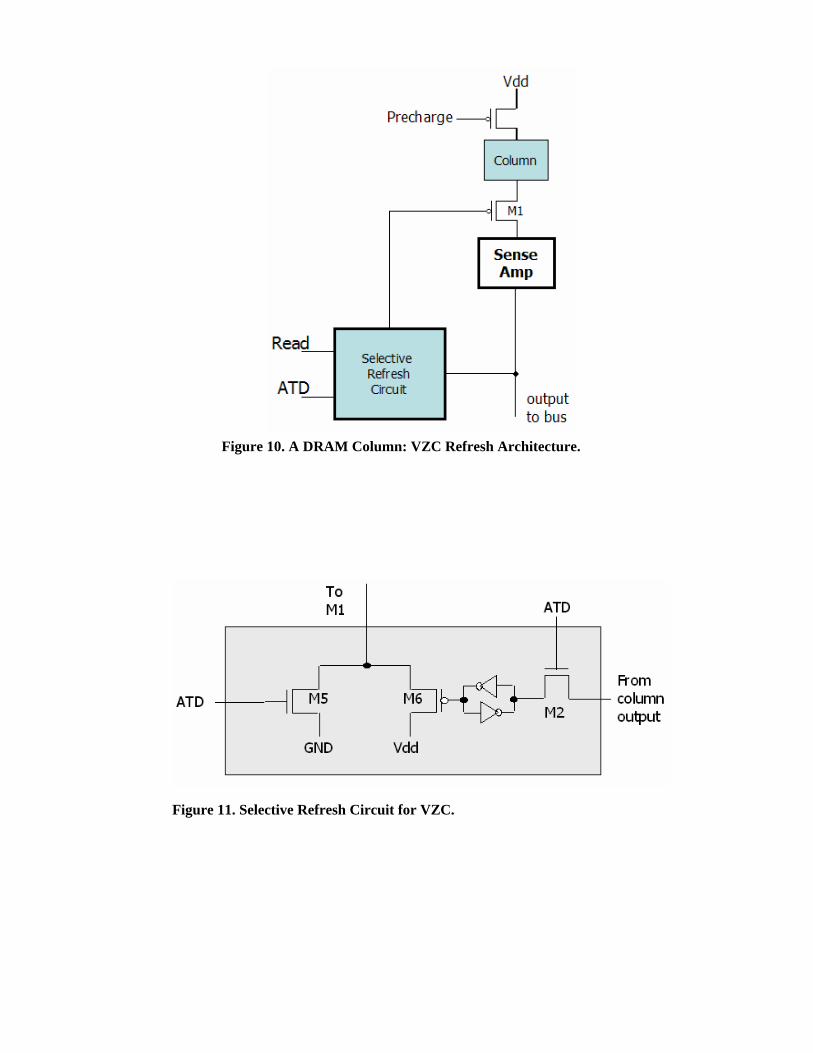
Figure 10. A DRAM Column: VZC Refresh Architecture.
Figure 11. Selective Refresh Circuit for VZC.

Figure 12. DRAM Column: VZC Update Architecture.
Figure 13. Write Circuit of Zero Indicator Bit (ZIB).

Figure 14. Operations During Refresh Period: VZC Architecture.
Figure 15. Write Analysis for MediaBench Applications
Figure 16. HZC: Relative Refresh Energy Savings in Encoding Applications
Figure 17. VZC: Relative Refresh Energy Savings in Encoding Applications

Figure 18. HZC: Relative Refresh Energy Savings in Decoding Applications
Figure 19.VZC: Relative Refresh Energy Savings in Decoding Applications

Table 1
RELATIVE PERCENTAGE AREA OVERHEAD
HZC VZC Components
n=8 n=16
n=32
n=8 n=16
n=32
Data Matrix 37.5 18.7 9.3 12.5 6.25 3.12
Bitline 12.5 6.25 3.12 100
Wordline 100 12.5 6.25 3.12 Sel. Refresh Negligible constant overhead
Row Decoder No overhead 9-10 3-4 1-2

BIOGRAPHIES
Kimish Patel has received his Bachelor’s of Engineering degree in Information Technology from
Nirma Institute of Technology, Gujarat University, India in July 2002. He is pursuing his PhD degree
in Computer Engineering at Politecnico di Torino, Italy since Jan 2004. His research interests are
mainly in low power design of memories and architecture of computer systems.
Enrico Macii (M’95, S’02, F’05) is a Professor of Electrical and Computer Engineering at
Politecnico di Torino. He holds a Dr.Eng. degree in Electrical Engineering from Politecnico di
Torino, a Dr.Sc. degree in Computer Science from Università di Torino, and a Ph.D. degree in
Computer Engineering from Politecnico di Torino. His research interests include several aspects of
the computer-aided design of digital integrated circuits and systems, with particular emphasis on
logic synthesis, optimization, and formal verification. He is Editor in Chief of the IEEE Transactions
on Computer-Aided Design of Integrated Circuits and Systems, and an Associate Editor of the ACM
Transactions on Design Automation of Electronic Systems. Prof. Macii is an Elected Member of the
Board of Governors of the IEEE Circuits and Systems Society since 2002.
Massimo Poncino (M’97) is an Associate Professor of Computer Science at Politecnico di Torino.
He received a Dr.Eng. degree in Electrical Engineering and the Ph.D. degree in Computer
Engineering, both from Politecnico di Torino. His research interests include several aspects of design
automation of digital systems, with particular emphasis on the modeling and optimization of low-
power systems. He has co-authored over 180 journal and conference papers, as well as a book on
low-power memory design. He is an Associate Editor of the IEEE Transactions on Computer-Aided
Design of Integrated Circuits and Systems, and a member of the technical program committee of

several technical conferences, including the International Symposium on Low Power Design.
Luca Benini (S’94–M’97) is an Associate Professor at the Department of Electrical Engineering and
Computer Science (DEIS) of the University of Bologna. He received a Ph.D. degree in electrical
engineering from Stanford University in 1997. He also holds visiting researcher positions at Stanford
University and the Hewlett-Packard Laboratories, Palo Alto, CA. Dr. Benini's research interests are
in computer architecture and computer-aided design of digital systems, with special emphasis on
low-power applications and SoC design. On these topics he has published more than 200 papers in
international journals and conferences and three books. He has been program chair and vice-chair of
Design Automation and Test in Europe Conference He is a member of the technical program
committee and organizing committee of several technical conferences, including the Design
Automation Conference, International Symposium on Low Power Design, the Symposiom on
Hardware-Software Codesign.