Measurement of neutron-proton capture in the SNO$+$ water ...
ENERGY DEPOSITION MECHANISMS FOR PROTON- AND
NEUTRON-INDUCED SINGLE EVENT UPSETS
IN MODERN ELECTRONIC DEVICES
By
Michael Andrew Clemens
Dissertation
Submitted to the Faculty of the
Graduate School of Vanderbilt University
in partial fulfillment of the requirements
for the degree of
DOCTOR OF PHILOSOPHY
in
Physics
May 2012
Nashville, Tennessee
Approved:
Professor Robert A. Weller
Professor Robert A. Reed
Professor Marcus H. Mendenhall
Professor Sokrates T. Pantelides
Professor Volker E. Oberacker
To my children:May you forever feel the need to discover
ii
ACKNOWLEDGMENTS
I am indebted to many people who have helped me over the course of
my graduate studies. First and foremost, I would like to express my deep
appreciation and love to my wife, Michelle, for her tremendous encouragement
and support. Without her, I certainly wouldn’t be where I am today.
Much of the experimental portion of this work was made possible by the
help and friendship of my colleague Nathaniel Dodds. From building and
debugging the pulse height analysis system, to packing equipment and ac-
companying me on numerous trips to cyclotron facilities, his assistance was
invaluable. I am also deeply appreciative of the advice and help I’ve received
from my advisor, Prof. Robert Weller, as well as Profs. Marcus Mendenhall
and Robert Reed. The assistance I’ve received from these three professors
has been selfless and essential in my scientific endeavors. I would also like to
thank Nick Hooten for his help and useful discussions. Additionally I would
like to acknowledge my colleagues from Sandia National Laboratories, Marty
Shaneyfelt, Paul Dodd, and Jim Schwank for their help in obtaining the diodes
used in this study and for useful feedback in my work. I would like to thank
Ewart Blackmore and Michael Trinczek for their help in using the facilities at
TRIUMF, and also Steve Wender for his help in my experiment at the Los
Alamos neutron beam facility. Steve went above and beyond what was re-
quired of him to make sure that I was able to obtain useful data, and I thank
him for that.
The computational part of this work was conducted through Vanderbilt
University’s Advanced Computing Center for Research and Education (AC-
CRE). Funding for this work was provided by the Defense Threat Reduction
iii
Agency under grants HDTRA 1-08-1-0033 and HDTRA 1-08-1-0034, and in
part by the NASA Electronics Parts and Packaging Program and the De-
partment of Defense Science Mathematics and Research for Transformation
(SMART) Scholarship for Service Program.
Lastly, I would like to thank my parents, Marc and Monica, for their ex-
amples of hard work and integrity, and for encouraging me throughout my life
to do my best. Much of who I am I owe to them.
iv
TABLE OF CONTENTS
DEDICATION iii
ACKNOWLEDGMENTS v
LIST OF TABLES vii
LIST OF FIGURES viii
I INTRODUCTION 1
II BACKGROUND 6Radiation Environments . . . . . . . . . . . . . . . . . . . . . . . . . . . . 6
Space . . . . . . . . . . . . . . . . . . . . . . . . . . . . . . . . . . . . 7Terrestrial Level . . . . . . . . . . . . . . . . . . . . . . . . . . . . . . 8
Single Event Upsets (SEUs) . . . . . . . . . . . . . . . . . . . . . . . . . . 9Linear Energy Transfer . . . . . . . . . . . . . . . . . . . . . . . . . . . . . 11Critical Charge . . . . . . . . . . . . . . . . . . . . . . . . . . . . . . . . . 14Monte Carlo Simulation . . . . . . . . . . . . . . . . . . . . . . . . . . . . 15Sensitive Volume Modeling for SEUs . . . . . . . . . . . . . . . . . . . . . 17Single and Multiple Bit Upsets . . . . . . . . . . . . . . . . . . . . . . . . 19Proton and Neutron-Induced SEUs - Nuclear Reactions . . . . . . . . . . . 21
IIIEXPERIMENTAL AND SIMULATION METHODS 27Charge collection measurements . . . . . . . . . . . . . . . . . . . . . . . . 27
Pulse height analysis (PHA) . . . . . . . . . . . . . . . . . . . . . . . 2716 channel PHA system . . . . . . . . . . . . . . . . . . . . . . . . . 33Diode Structures . . . . . . . . . . . . . . . . . . . . . . . . . . . . . 35
Particle Beam Experiments . . . . . . . . . . . . . . . . . . . . . . . . . . 39Proton Irradiations . . . . . . . . . . . . . . . . . . . . . . . . . . . . 39Neutron Irradiations . . . . . . . . . . . . . . . . . . . . . . . . . . . 40
Time of Flight (TOF) Measurements . . . . . . . . . . . . . . . . . . . . . 42Description of TOF setup . . . . . . . . . . . . . . . . . . . . . . . . 42TOF Calculation . . . . . . . . . . . . . . . . . . . . . . . . . . . . . 43
Monte Carlo Simulations . . . . . . . . . . . . . . . . . . . . . . . . . . . . 46Description of Simulation Tool . . . . . . . . . . . . . . . . . . . . . . 46Uses of Simulation Tool . . . . . . . . . . . . . . . . . . . . . . . . . 47Nuclear Physics Models . . . . . . . . . . . . . . . . . . . . . . . . . . 48
v
IV MECHANISMS OF PROTON-INDUCED SINGLE EVENT EF-FECTS 50Introduction . . . . . . . . . . . . . . . . . . . . . . . . . . . . . . . . . . . 50Charge Collection Measurements . . . . . . . . . . . . . . . . . . . . . . . 52Monte Carlo Simulations . . . . . . . . . . . . . . . . . . . . . . . . . . . . 57
Model Validation . . . . . . . . . . . . . . . . . . . . . . . . . . . . . 57Proton-Induced Nuclear Reactions . . . . . . . . . . . . . . . . . . . . 60
Conclusions . . . . . . . . . . . . . . . . . . . . . . . . . . . . . . . . . . . 63
V MECHANISMS OF NEUTRON-INDUCED SINGLE EVENT EF-FECTS 64Introduction . . . . . . . . . . . . . . . . . . . . . . . . . . . . . . . . . . . 64Charge Collection Measurements . . . . . . . . . . . . . . . . . . . . . . . 66SEU and MCU Simulations . . . . . . . . . . . . . . . . . . . . . . . . . . 68
Monte Carlo Simulations . . . . . . . . . . . . . . . . . . . . . . . . . 68E↵ect of W Overlayer on MCU Response . . . . . . . . . . . . . . . . 70WNR and 14 MeV Neutron Spectra Compared . . . . . . . . . . . . . 72E↵ect of Neutron Energy on MCUs . . . . . . . . . . . . . . . . . . . 78
Conclusions . . . . . . . . . . . . . . . . . . . . . . . . . . . . . . . . . . . 81
VI CONCLUSIONS 83
A LINEAR ENERGY TRANSFER 85Overview . . . . . . . . . . . . . . . . . . . . . . . . . . . . . . . . . . 85Physics of LET . . . . . . . . . . . . . . . . . . . . . . . . . . . . . . 86Accuracy of LET Theory . . . . . . . . . . . . . . . . . . . . . . . . . 89
B MRED STANDARD MODE EXAMPLE CODE 91
C MRED SINGLE EVENT MODE EXAMPLE CODE 97
BIBLIOGRAPHY 107
vi
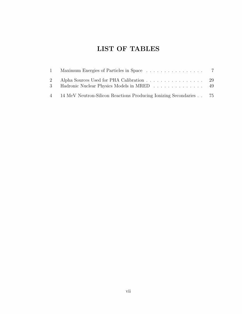
LIST OF TABLES
1 Maximum Energies of Particles in Space . . . . . . . . . . . . . . . . 7
2 Alpha Sources Used for PHA Calibration . . . . . . . . . . . . . . . . 293 Hadronic Nuclear Physics Models in MRED . . . . . . . . . . . . . . 49
4 14 MeV Neutron-Silicon Reactions Producing Ionizing Secondaries . . 75
vii
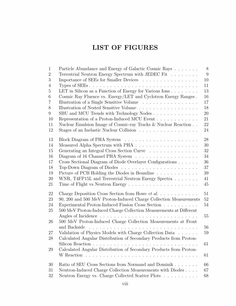
LIST OF FIGURES
1 Particle Abundance and Energy of Galactic Cosmic Rays . . . . . . . 82 Terrestrial Neutron Energy Spectrum with JEDEC Fit . . . . . . . . 93 Importance of SEEs for Smaller Devices . . . . . . . . . . . . . . . . 104 Types of SEEs . . . . . . . . . . . . . . . . . . . . . . . . . . . . . . . 115 LET in Silicon as a Function of Energy for Various Ions . . . . . . . . 136 Cosmic Ray Fluence vs. Energy/LET and Cyclotron Energy Ranges . 167 Illustration of a Single Sensitive Volume . . . . . . . . . . . . . . . . 178 Illustration of Nested Sensitive Volume . . . . . . . . . . . . . . . . . 189 SBU and MCU Trends with Technology Nodes . . . . . . . . . . . . . 2010 Representation of a Proton-Induced MCU Event . . . . . . . . . . . . 2111 Nuclear Emulsion Image of Cosmic-ray Tracks & Nuclear Reaction . . 2212 Stages of an Inelastic Nuclear Collision . . . . . . . . . . . . . . . . . 24
13 Block Diagram of PHA System . . . . . . . . . . . . . . . . . . . . . 2814 Measured Alpha Spectrum with PHA . . . . . . . . . . . . . . . . . . 3015 Generating an Integral Cross Section Curve . . . . . . . . . . . . . . 3216 Diagram of 16 Channel PHA System . . . . . . . . . . . . . . . . . . 3417 Cross Sectional Diagram of Diode Overlayer Configurations . . . . . . 3618 Top-Down Diagram of Diodes . . . . . . . . . . . . . . . . . . . . . . 3719 Picture of PCB Holding the Diodes in Beamline . . . . . . . . . . . . 3920 WNR, T4FP15L and Terrestrial Neutron Energy Spectra . . . . . . . 4121 Time of Flight vs Neutron Energy . . . . . . . . . . . . . . . . . . . . 45
22 Charge Deposition Cross Section from Howe et al. . . . . . . . . . . . 5123 90, 200 and 500 MeV Proton-Induced Charge Collection Measurements 5224 Experimental Proton-Induced Fission Cross Section . . . . . . . . . . 5425 500 MeV Proton-Induced Charge Collection Measurements at Di↵erent
Angles of Incidence . . . . . . . . . . . . . . . . . . . . . . . . . . . . 5526 500 MeV Proton-Induced Charge Collection Measurements at Front
and Backside . . . . . . . . . . . . . . . . . . . . . . . . . . . . . . . 5627 Validation of Physics Models with Charge Collection Data . . . . . . 5928 Calculated Angular Distribution of Secondary Products from Proton-
Silicon Reaction . . . . . . . . . . . . . . . . . . . . . . . . . . . . . . 6129 Calculated Angular Distribution of Secondary Products from Proton-
W Reaction . . . . . . . . . . . . . . . . . . . . . . . . . . . . . . . . 61
30 Ratio of SEU Cross Sections from Normand and Dominik . . . . . . . 6631 Neutron-Induced Charge Collection Measurements with Diodes . . . . 6732 Neutron Energy vs. Charge Collected Scatter Plots . . . . . . . . . . 68
viii
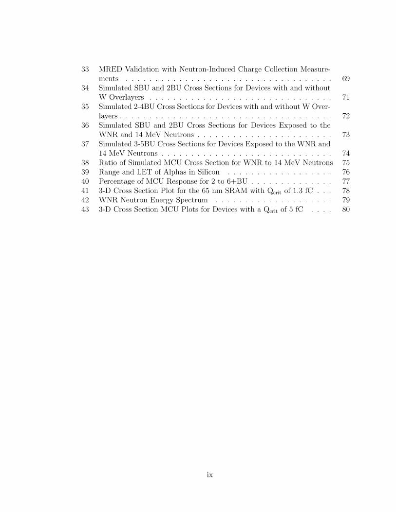
33 MRED Validation with Neutron-Induced Charge Collection Measure-ments . . . . . . . . . . . . . . . . . . . . . . . . . . . . . . . . . . . 69
34 Simulated SBU and 2BU Cross Sections for Devices with and withoutW Overlayers . . . . . . . . . . . . . . . . . . . . . . . . . . . . . . . 71
35 Simulated 2-4BU Cross Sections for Devices with and without W Over-layers . . . . . . . . . . . . . . . . . . . . . . . . . . . . . . . . . . . . 72
36 Simulated SBU and 2BU Cross Sections for Devices Exposed to theWNR and 14 MeV Neutrons . . . . . . . . . . . . . . . . . . . . . . . 73
37 Simulated 3-5BU Cross Sections for Devices Exposed to the WNR and14 MeV Neutrons . . . . . . . . . . . . . . . . . . . . . . . . . . . . . 74
38 Ratio of Simulated MCU Cross Section for WNR to 14 MeV Neutrons 7539 Range and LET of Alphas in Silicon . . . . . . . . . . . . . . . . . . 7640 Percentage of MCU Response for 2 to 6+BU . . . . . . . . . . . . . . 7741 3-D Cross Section Plot for the 65 nm SRAM with Qcrit of 1.3 fC . . . 7842 WNR Neutron Energy Spectrum . . . . . . . . . . . . . . . . . . . . 7943 3-D Cross Section MCU Plots for Devices with a Qcrit of 5 fC . . . . 80
ix
CHAPTER I
INTRODUCTION
Over the past 50+ years, computers have become increasingly powerful and ever-
present, appearing in an increasing number of modern devices. The individual com-
ponents of the integrated circuits (ICs) in computers have shrunk to sub-micron sizes
following a well-known trend known as Moore’s law [1]. While the shrinking of IC
component size has e↵ectively increased computer power, speed and lowered cost,
the decrease in feature size has not come without consequences. One of the conse-
quences for semiconducting devices has been an increased susceptibility to failure by
a mechanism that was predicted about 50 years ago.
In 1962, Wallmark and Marcus [2] published a prediction that ionizing radiation
would be able to upset the normal operation of electronic devices as their dimensions
decreased with the advance of technology. They postulated that smaller devices would
be more susceptible to cosmic ray radiation, and concluded that this would impose
a lower limit on the size of silicon-based devices (interestingly, the minimum device
volume they predicted was 10 µm3). Although it hasn’t yet restricted the practical
dimensions of electronic devices, the postulate of upset susceptibility increasing with
smaller devices has proved generally true. However, it wasn’t until the 1970’s that this
e↵ect was observed. Anomalies in orbiting communications satellites were observed
in 1975 by Binder et al. [3] who attributed the anomalies to cosmic ray radiation.
In 1979, errors were observed by May and Woods [4] in ground-based DRAMs and
CCDs which were attributed to alpha particles emitted by radioactive isotopes of
uranium and thorium in parts-per-million levels in packaging materials. Since that
1
time electronic devices have shrunk in size by many orders of magnitude (beyond
10 µm3) and the interest in radiation e↵ects has grown accordingly, particularly for
space-bound electronics.
Of the types of radiation e↵ects that plague modern-day electronic devices, single
event e↵ects (SEEs - radiation e↵ects caused by a single particle strike) have be-
come increasingly important. A subset of SEEs, the single event upset (SEU), is the
topic of this dissertation. This dissertation presents new research which furthers the
understanding of mechanisms behind SEUs in modern-day devices, both for devices
exposed to the natural space radiation environment and that of the terrestrial level.
In space, the dominant form of radiation is energetic protons. However, because
of their single electric charge, most of the energetic protons found in space do not
have a high enough linear energy transfer (LET - a measure of how much charge an
energetic particle will deposit in a material it traverses) to cause SEUs through direct
ionization. Instead, proton-induced SEUs are typically caused by secondary particles
that result from proton-nuclei collisions in materials in or near a sensitive node in
the semiconducting device. These secondary particles are either nuclei recoils from
elastic collisions, or nuclear fragments from inelastic collisions. In either case, it is the
heavy-ion secondary products that are often the mechanism of proton-induced SEUs.
Thus, accurate computer simulation of proton-induced radiation e↵ects becomes, in
part, a question of correct nuclear physics modeling, as well as particle transport and
energy deposition calculations.
The role of high atomic number (high-Z) materials found in modern-day devices,
such as tungsten (W), in proton-induced radiation e↵ects is not fully understood.
Howe et al. [5] published Monte Carlo calculations which predicted that, when irra-
diated with protons, devices containing W overlayers would have the same radiation
response as devices with similarly placed oxide layers. Conversely, Schwank et al. [6]
2
observed proton-induced radiation e↵ects in static random access memories (SRAMs)
which could not be explained by only considering proton-silicon reactions. Through
simulations, they concluded that the observed e↵ects were possibly caused by higher-
LET secondary particles from proton collisions with high-Z materials in the SRAMs.
Chapter IV of this dissertation presents new experimental and Monte Carlo sim-
ulation data which demonstrate that the presence of W in a device can significantly
increase the e↵ects of proton-induced radiation due to proton-induced fission in W.
Proton-induced fission is shown to occur in W for incident protons with su�ciently
high energy (>⇠100 MeV). It is shown that the high-LET secondaries from proton-
induced fission are su�ciently ionizing to cause the e↵ects reported by Schwank et
al. [6]. Additionally, it is found that the prediction reported by Howe et al. is inaccu-
rate due to the miscalculation of proton-induced fission in W by the nuclear physics
model used in their work. With the increasing diversity of materials found in today’s
semiconductor devices, it is apparent that nuclear physics models used for radiation
e↵ects prediction must not only model proton-silicon interactions correctly, but also
proton interactions with high-Z materials.
At a terrestrial level, one of the major causes of radiation e↵ects in electronics
is neutrons originating from cosmic-ray particles colliding with nuclei in atmospheric
atoms. Because of their neutral charge, the neutrons produced in such collisions
are able to reach the earth’s surface in a significant number spanning energies from
less than 1 eV to up to 100s of GeV [7]. In recent years, neutron-induced radiation
e↵ects have become a major concern for the reliability of modern and developing
semiconductor technologies [8,9]. While much research has been done on the subject
matter, the e↵ect that high-Z materials can have on neutron-induced SEUs has not
been investigated.
Chapter V of this dissertation presents experimental and Monte Carlo simula-
3
tion data which show that neutron-induced fission in W can increase the e↵ects of
terrestrial-level radiation. Like proton-induced fission, these events only occur for
high-energy neutrons and can also produce high-LET secondary particles. However,
the data shown here suggest that the presence of W would only significantly increase
neutron-induced SEUs only for radiation hardened devices resistant to SEUs. This is
due, in part, to the relatively small number of high energy neutrons which are able
to cause neutron-induced fission in W.
Because of the natural neutron radiation at a terrestrial level, computer chip
makers must now qualify their electronic parts that are to be used in an unshielded
environment. It is ideal to qualify parts in a radiation environment that is as similar to
the natural one as possible. There are a few facilities that provide accelerated neutron
testing with an energy spectrum similar to that of the natural terrestrial environment,
among them is the Los Alamos National Laboratories’ Weapons Nuclear Research
(WNR) facility [10]. However, due to cost and accessibility, alternative test methods
for neutron vulnerability of electronic devices have been investigated [11, 12]. One
of the more prominent alternatives is using a monoenergetic 14 MeV neutron beam
generated by a fusion reaction of deuterium and tritium [13]. How well the 14 MeV
neutron beam is able to assess radiation susceptibility of an electronic device is the
topic of much debate and research. In [12], a comparison was made of the SEU cross
sections measured using a 14 MeV neutron source and the WNR neutron spectrum. It
was observed that, for multiple static random access memories (SRAMs) from various
technology nodes, the SEU cross section measured using 14 MeV neutrons was within
a factor of two of that measured using WNR neutrons. The smallest technology node
measured in this study was 90 nm, and the analysis was only done for single bit upsets
(SBUs) and not multiple cell upsets (MCUs - when more than one bit is upset by a
single incident neutron).
4
Chapter V of this dissertation presents new Monte Carlo simulation results which
compare the SBU and MCU cross sections for a 65 nm SRAM irradiated with the
WNR neutron spectrum and 14 MeV neutrons. These results show that the SBU cross
section caused by WNR and 14 MeV neutrons in this device agree to within factor
of two, in agreement with the trend shown in [12]. However, the 14 MeV neutrons
under predict the MCU cross section when compared with the WNR neutrons, for
the device considered here. The mechanism behind the 14 MeV-neutron-induced
MCU events is investigated and shown to be secondary alpha particles from inelastic
neutron-silicon collisions. These secondary alpha particles have a high enough LET
and range to cause multiple bits to upset in the SRAM at a significant cross section.
Higher-energy neutrons in the WNR neutron spectrum are able to cause MCU events
through heavy ion secondary particles and silicon nuclei recoils. These secondaries
are able to deposit more charge over a longer range. For this reason, 14 MeV neutrons
under predict the WNR neutron MCU cross section for the device considered here.
The original research which is presented in this dissertation spanned the years
2008-2011. The results of this work have been presented at the Nuclear and Space
Radiation E↵ects Conference over the course of those years and published [14, 15] in
the peer-reviewed journal IEEE Transactions on Nuclear Science, the premier journal
for radiation e↵ects publications.
5
CHAPTER II
BACKGROUND
This chapter gives an introduction to and overview of the study of radiation e↵ects
on electronic devices, focusing on the physics and modeling techniques relevant to the
research presented in this work. All of the radiation-e↵ects-specific terms that are
used in later chapters are defined in this chapter as well. The mechanisms of proton-
and neutron-induced single event upsets, which is the topic of this document, can be
understood, and are placed in context, by the concepts discussed in this chapter.
Radiation Environments
Companies which design and make electronic components must understand the nat-
ural radiation environments which those parts will encounter during their lifetime of
use. In many cases, these companies must also test their parts by irradiation with
man-made particle accelerators. Historically, this has been more critical for parts
designed for satellites and aircraft because of the comparatively harsh radiation en-
vironment in low-earth orbit and at aircraft cruising altitudes. However, in recent
years, even parts made for use at sea level have been su�ciently sensitive to upset
that they must be qualified for that radiation environment by irradiation with neu-
trons. This section discusses the radiation environments found in space, and also at
a terrestrial level.
6
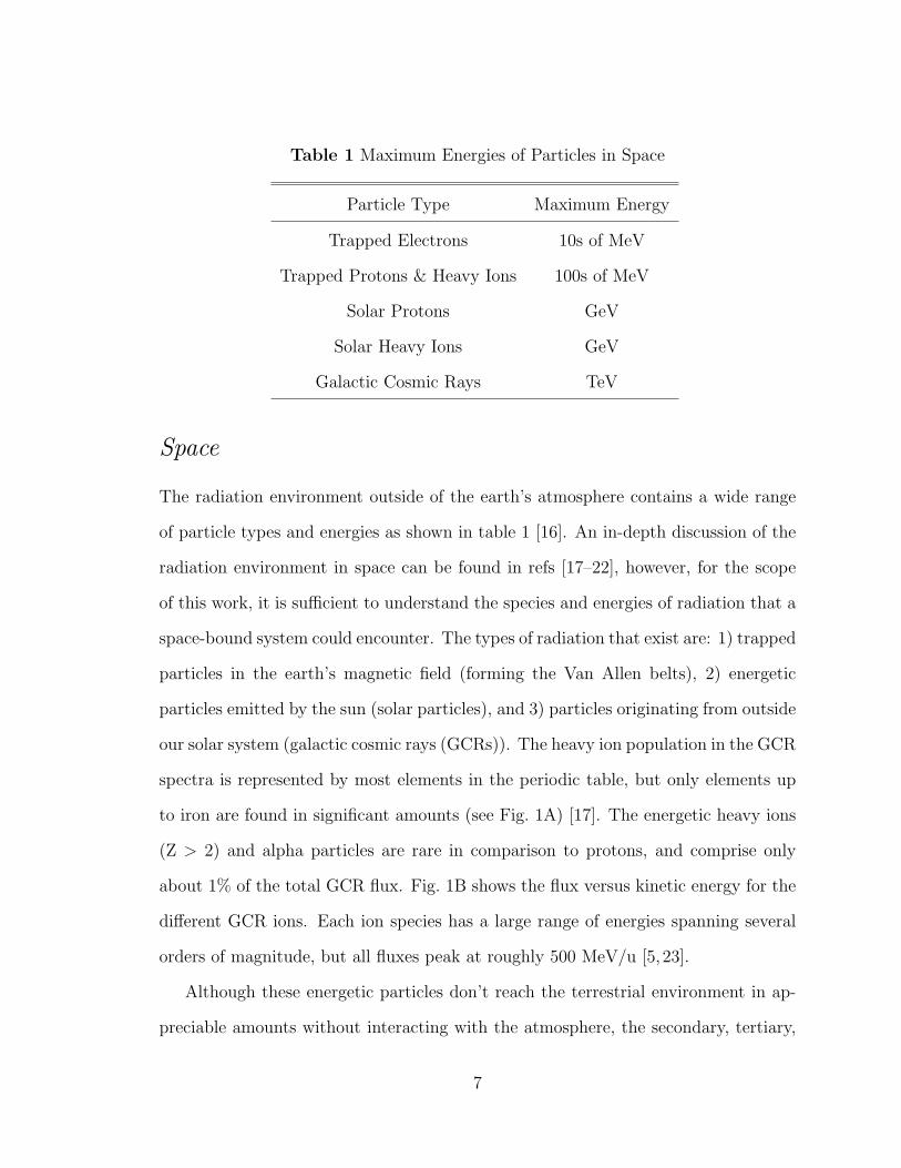
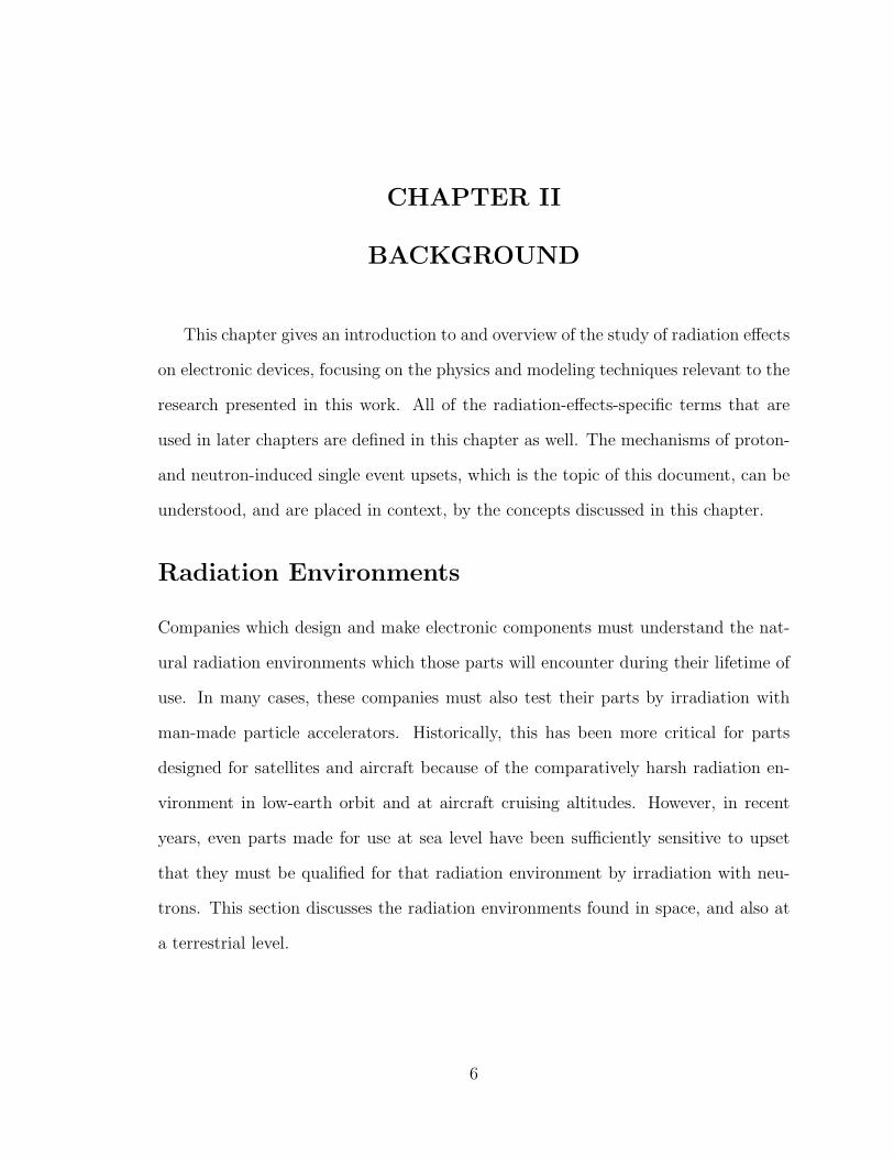
Table 1 Maximum Energies of Particles in Space
Particle Type Maximum Energy
Trapped Electrons 10s of MeV
Trapped Protons & Heavy Ions 100s of MeV
Solar Protons GeV
Solar Heavy Ions GeV
Galactic Cosmic Rays TeV
Space
The radiation environment outside of the earth’s atmosphere contains a wide range
of particle types and energies as shown in table 1 [16]. An in-depth discussion of the
radiation environment in space can be found in refs [17–22], however, for the scope
of this work, it is su�cient to understand the species and energies of radiation that a
space-bound system could encounter. The types of radiation that exist are: 1) trapped
particles in the earth’s magnetic field (forming the Van Allen belts), 2) energetic
particles emitted by the sun (solar particles), and 3) particles originating from outside
our solar system (galactic cosmic rays (GCRs)). The heavy ion population in the GCR
spectra is represented by most elements in the periodic table, but only elements up
to iron are found in significant amounts (see Fig. 1A) [17]. The energetic heavy ions
(Z > 2) and alpha particles are rare in comparison to protons, and comprise only
about 1% of the total GCR flux. Fig. 1B shows the flux versus kinetic energy for the
di↵erent GCR ions. Each ion species has a large range of energies spanning several
orders of magnitude, but all fluxes peak at roughly 500 MeV/u [5, 23].
Although these energetic particles don’t reach the terrestrial environment in ap-
preciable amounts without interacting with the atmosphere, the secondary, tertiary,
7
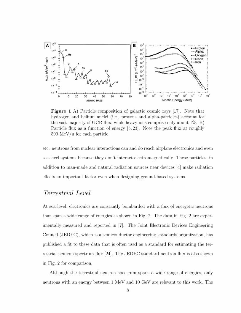
Figure 1 A) Particle composition of galactic cosmic rays [17]. Note thathydrogen and helium nuclei (i.e., protons and alpha-particles) account forthe vast majority of GCR flux, while heavy ions comprise only about 1%. B)Particle flux as a function of energy [5, 23]. Note the peak flux at roughly500 MeV/u for each particle.
etc. neutrons from nuclear interactions can and do reach airplane electronics and even
sea-level systems because they don’t interact electromagnetically. These particles, in
addition to man-made and natural radiation sources near devices [4] make radiation
e↵ects an important factor even when designing ground-based systems.
Terrestrial Level
At sea level, electronics are constantly bombarded with a flux of energetic neutrons
that span a wide range of energies as shown in Fig. 2. The data in Fig. 2 are exper-
imentally measured and reported in [7]. The Joint Electronic Devices Engineering
Council (JEDEC), which is a semiconductor engineering standards organization, has
published a fit to these data that is often used as a standard for estimating the ter-
restrial neutron spectrum flux [24]. The JEDEC standard neutron flux is also shown
in Fig. 2 for comparison.
Although the terrestrial neutron spectrum spans a wide range of energies, only
neutrons with an energy between 1 MeV and 10 GeV are relevant to this work. The
8
Figure 2 Measured terrestrial neutron energy spectrum [7] plotted with thepublished JEDEC fit to the data [24].
lower-energy neutrons (< 1 MeV) are not considered here because they do not have
su�cient energy to produce a secondary particle in a device which has a high enough
LET to cause a single event upset. The higher-energy neutrons are not considered
here because their flux is su�ciently low that e↵ects due to these neutrons are so rare
as to be negligible.
Single Event Upsets (SEUs)
Radiation e↵ects research focuses on either the sustained degradation in a device over
a long period of radiation exposure (total dose), the degradation of a device due to
displacement of atoms in the silicon lattice due to nuclear collisions (displacement
damage) or the errors due to a single strike of an energetic ion in a device (single
event e↵ects (SEEs)) [25–27]. The two e↵ects which are most commonly the subject
of research are total dose e↵ects and SEEs. Historically, total dose e↵ects have been
the most prominent radiation e↵ect in devices. However, as technology has advanced,
9
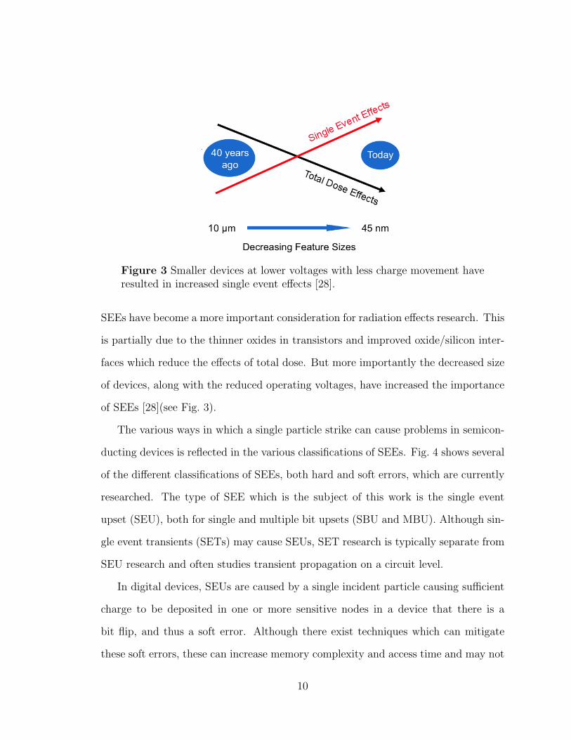
Figure 3 Smaller devices at lower voltages with less charge movement haveresulted in increased single event e↵ects [28].
SEEs have become a more important consideration for radiation e↵ects research. This
is partially due to the thinner oxides in transistors and improved oxide/silicon inter-
faces which reduce the e↵ects of total dose. But more importantly the decreased size
of devices, along with the reduced operating voltages, have increased the importance
of SEEs [28](see Fig. 3).
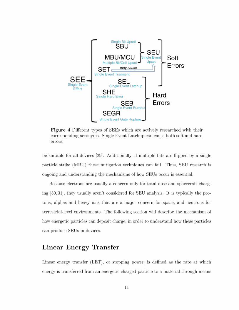
The various ways in which a single particle strike can cause problems in semicon-
ducting devices is reflected in the various classifications of SEEs. Fig. 4 shows several
of the di↵erent classifications of SEEs, both hard and soft errors, which are currently
researched. The type of SEE which is the subject of this work is the single event
upset (SEU), both for single and multiple bit upsets (SBU and MBU). Although sin-
gle event transients (SETs) may cause SEUs, SET research is typically separate from
SEU research and often studies transient propagation on a circuit level.
In digital devices, SEUs are caused by a single incident particle causing su�cient
charge to be deposited in one or more sensitive nodes in a device that there is a
bit flip, and thus a soft error. Although there exist techniques which can mitigate
these soft errors, these can increase memory complexity and access time and may not
10
SBU!
SEE!
MBU/MCU!
SET!
SEL!
SEB!SEGR!
SHE!
SEU!Soft!Errors!
Hard!Errors!
Single Event Effect
Single Bit Upset
Multiple Bit/Cell Upset
Single Event Transient
Single Event Latchup
Single Hard Error
Single Event Burnout
Single Event Gate Rupture
Single Event Upset
may cause
Figure 4 Di↵erent types of SEEs which are actively researched with theircorresponding acronyms. Single Event Latchup can cause both soft and harderrors.
be suitable for all devices [29]. Additionally, if multiple bits are flipped by a single
particle strike (MBU) these mitigation techniques can fail. Thus, SEU research is
ongoing and understanding the mechanisms of how SEUs occur is essential.
Because electrons are usually a concern only for total dose and spacecraft charg-
ing [30, 31], they usually aren’t considered for SEU analysis. It is typically the pro-
tons, alphas and heavy ions that are a major concern for space, and neutrons for
terrestrial-level environments. The following section will describe the mechanism of
how energetic particles can deposit charge, in order to understand how these particles
can produce SEUs in devices.
Linear Energy Transfer
Linear energy transfer (LET), or stopping power, is defined as the rate at which
energy is transferred from an energetic charged particle to a material through means
11
of an electromagnetic interaction between them. This happens through a series of
collisions between the incident particle and the atoms in the material. The result
is either the excitation or the ionization of the target atom, and a loss of kinetic
energy for the incident particle. The mathematical expression for LET is given by
the Bethe-Bloch equation [32]:
LET = Kz2Z
A
1
�2
⇥L0(�) + zL1(�) + z2L2(�)...
⇤(1)
where K is a constant, z is the atomic number of the incident ion, Z and A are
the atomic and mass number of the target atoms, and � is v/c for the incident ion.
The term in brackets is the expansion of the stopping number, L(�) which is actually
a function of various terms other than �. The origin of Eq. 1 is covered in depth in
Appendix A. LET is most commonly expressed in units of MeV·cm2/mg.
In semiconducting materials, charge is generated when enough energy is trans-
ferred to the material to excite electrons from the conduction band to the valence
band creating an electron-hole pair. In silicon (the semiconductor of choice for most
modern electronic devices), the average energy required to generate an electron-hole
pair is 3.6 eV [33]. Thus the conversion from energy transferred (as calculated with
Eq. 1) to charge deposited is 22.5 MeV/pC.
If the density of the material, ⇢, that the energetic particle is traversing is known,
then one can multiply LET by the density to give energy loss in units of MeV/µm.
Using this we can calculate the amount of charge per unit length that is deposited
on average in a material for a given LET. For example, a particle with an LET
of 97 MeV·cm2/mg will deposit on average 1 pC/µm in silicon (⇢ = 2.33 g·cm�3),
assuming the LET doesn’t decrease appreciably over the distance in question.
It is critical to understand that the energy deposition process is highly stochas-
12
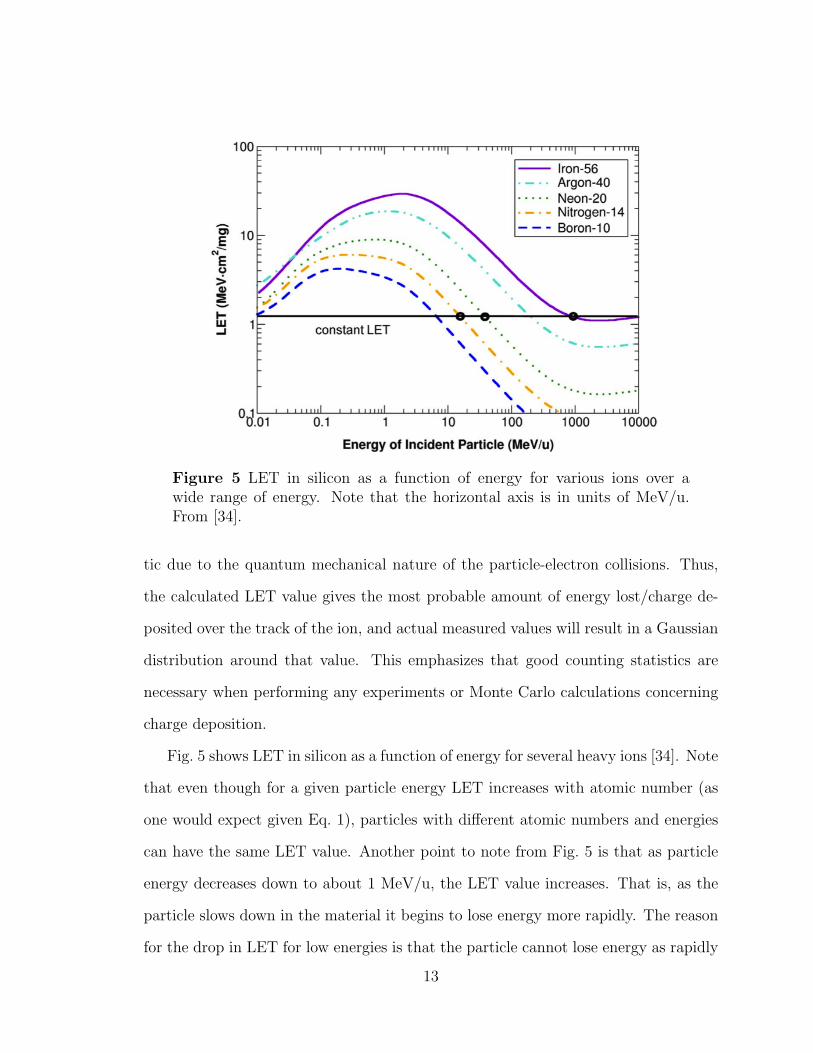
Figure 5 LET in silicon as a function of energy for various ions over awide range of energy. Note that the horizontal axis is in units of MeV/u.From [34].
tic due to the quantum mechanical nature of the particle-electron collisions. Thus,
the calculated LET value gives the most probable amount of energy lost/charge de-
posited over the track of the ion, and actual measured values will result in a Gaussian
distribution around that value. This emphasizes that good counting statistics are
necessary when performing any experiments or Monte Carlo calculations concerning
charge deposition.
Fig. 5 shows LET in silicon as a function of energy for several heavy ions [34]. Note
that even though for a given particle energy LET increases with atomic number (as
one would expect given Eq. 1), particles with di↵erent atomic numbers and energies
can have the same LET value. Another point to note from Fig. 5 is that as particle
energy decreases down to about 1 MeV/u, the LET value increases. That is, as the
particle slows down in the material it begins to lose energy more rapidly. The reason
for the drop in LET for low energies is that the particle cannot lose energy as rapidly
13
simply because it doesn’t have very much energy.
How much charge is deposited by an incident particle in a sensitive volume of a
device is dependent on the LET of the particle as it traverses the sensitive volume.
Whether or not an SEU occurs depends not only on the amount of charge deposited,
but also on the critical charge of the sensitive node. Critical charge is discussed in
the following section.
Critical Charge
When an energetic particle passes through a sensitive part of a semiconducting device
and deposits energy, it creates electron-hole pairs which can be swept away from
each other by an existing electric field in the area. These collected electrons and
holes constitute the collected charge from the single event. This collected charge
can cause a SEU in the device if the collected charge is equal to or larger than a
threshold value. This quantity is called the critical charge, Qcrit, and is dependent
only on the device, not the radiation environment [35]. Qcrit can be extracted from
experimental measurements or circuit simulation methods [36] and in practice, it is
often used as a figure of merit when comparing di↵erent devices and technologies.
In general, as devices are scaled down in size (with nothing else changed but the
size of the components), the Qcrit decreases and single event strikes that weren’t a
problem for larger devices become a serious issue for their smaller counterparts (see
Fig. 3). There are many techniques for radiation hardening of these smaller devices
that can, in e↵ect, increase the Qcrit and e↵ectively decrease the SEU rate in newer
technologies [37,38].
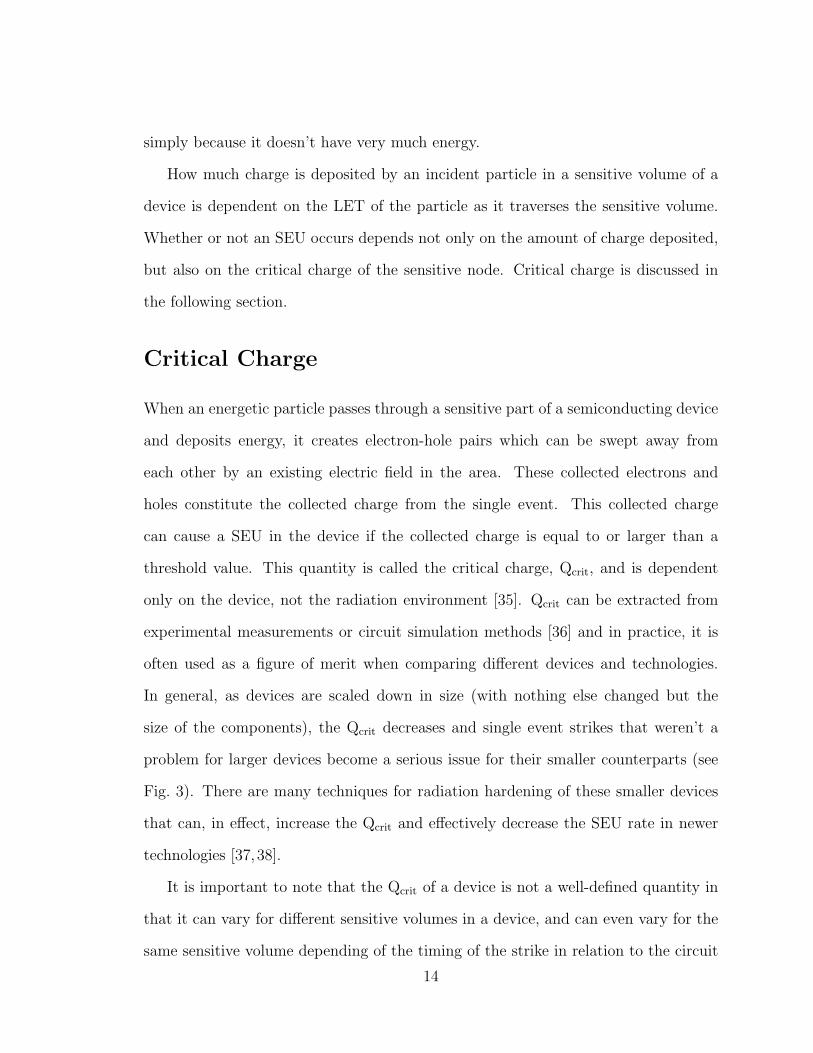
It is important to note that the Qcrit of a device is not a well-defined quantity in
that it can vary for di↵erent sensitive volumes in a device, and can even vary for the
same sensitive volume depending of the timing of the strike in relation to the circuit
14
dynamics [27]. The estimated Qcrit is then a best estimate of the amount of charge
necessary to cause an SEU. In Monte Carlo simulations of SEUs, Qcrit is necessarily
used to determine whether an incident ion causes an SEU or not. Therefore, Monte
Carlo simulation techniques shouldn’t be used without understanding the limitations
of the Qcrit value.
Monte Carlo Simulation
The high cost of putting electronics into space, only to have them fail when intro-
duced to the harsh radiation environment that exists there has led to techniques for
predicting SEE radiation susceptibility. The most predominant techniques are: 1)
testing devices at ground-based cyclotron facilities and 2) using Monte Carlo com-
puter simulations to predict SEU rates. A handful of cyclotron facilities exist that
are typically used for SEE testing, including cyclotrons located at Lawrence Berkeley
National Lab [39], Texas A&M University [40], and Indiana University [41]. While
there are a few facilities that are capable of producing beams of ions with energies
at or near the energy of galactic cosmic ray maximum flux, the beamtime at such
facilities is expensive and often not available.
Fig. 6 shows the energy range that is typically available at these facilities super-
imposed on the galactic cosmic ray spectra for iron. It is important to note that while
these facilities are only able to produce 1-100 MeV/u ions, they are in the range of
highest particle LET. It is clear from Fig. 6 that it is impossible to test parts in
the same radiation environment that they will be exposed to in space, and thus very
di�cult to predict exactly how a part will react to the harsh radiation environment
found there.
JEDEC has published guidelines for SEE testing of parts using energetic heavy ion
or proton beams at existing cyclotron facilities in order to best qualify parts [24,42].
15
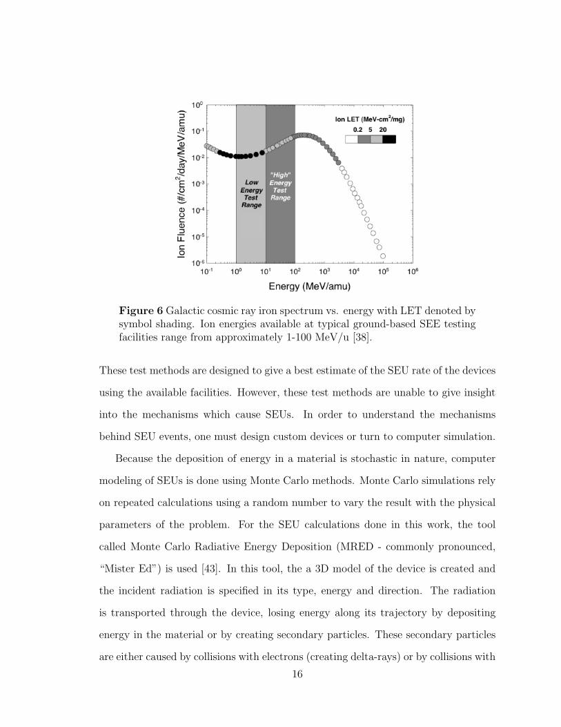
Figure 6 Galactic cosmic ray iron spectrum vs. energy with LET denoted bysymbol shading. Ion energies available at typical ground-based SEE testingfacilities range from approximately 1-100 MeV/u [38].
These test methods are designed to give a best estimate of the SEU rate of the devices
using the available facilities. However, these test methods are unable to give insight
into the mechanisms which cause SEUs. In order to understand the mechanisms
behind SEU events, one must design custom devices or turn to computer simulation.
Because the deposition of energy in a material is stochastic in nature, computer
modeling of SEUs is done using Monte Carlo methods. Monte Carlo simulations rely
on repeated calculations using a random number to vary the result with the physical
parameters of the problem. For the SEU calculations done in this work, the tool
called Monte Carlo Radiative Energy Deposition (MRED - commonly pronounced,
“Mister Ed”) is used [43]. In this tool, the a 3D model of the device is created and
the incident radiation is specified in its type, energy and direction. The radiation
is transported through the device, losing energy along its trajectory by depositing
energy in the material or by creating secondary particles. These secondary particles
are either caused by collisions with electrons (creating delta-rays) or by collisions with
16
nuclei, and these particles are also transported through the device, along a trajectory,
depositing energy. The physics models involved in MRED will not be discussed here,
but are discussed in section III. When simulations are run in MRED, the number of
incident ions must be high to obtain statically significant calculation, just like in an
experiment. An SEU is determined to occur if the amount of energy/charge deposited,
by either the incident particle or by a secondary particle, in a sensitive volume exceeds
the Qcrit of the device. The following section describes how the sensitive volumes are
defined in a device.
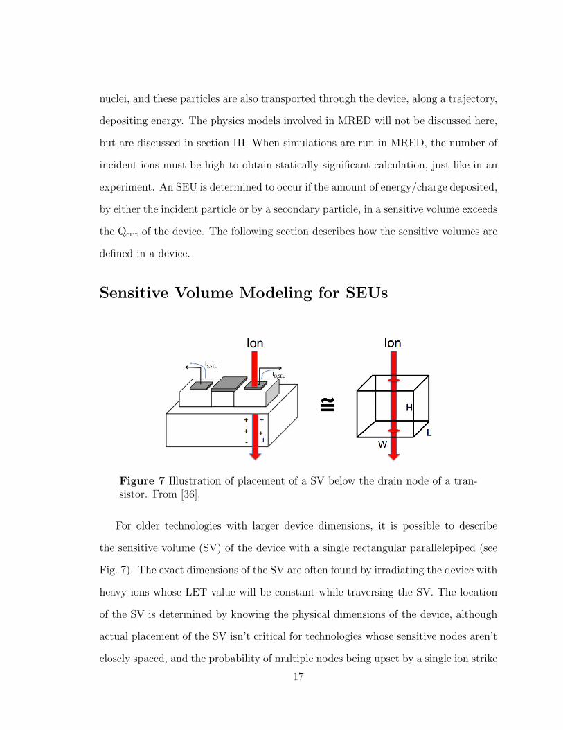
Sensitive Volume Modeling for SEUs
Figure 7 Illustration of placement of a SV below the drain node of a tran-sistor. From [36].
For older technologies with larger device dimensions, it is possible to describe
the sensitive volume (SV) of the device with a single rectangular parallelepiped (see
Fig. 7). The exact dimensions of the SV are often found by irradiating the device with
heavy ions whose LET value will be constant while traversing the SV. The location
of the SV is determined by knowing the physical dimensions of the device, although
actual placement of the SV isn’t critical for technologies whose sensitive nodes aren’t
closely spaced, and the probability of multiple nodes being upset by a single ion strike
17
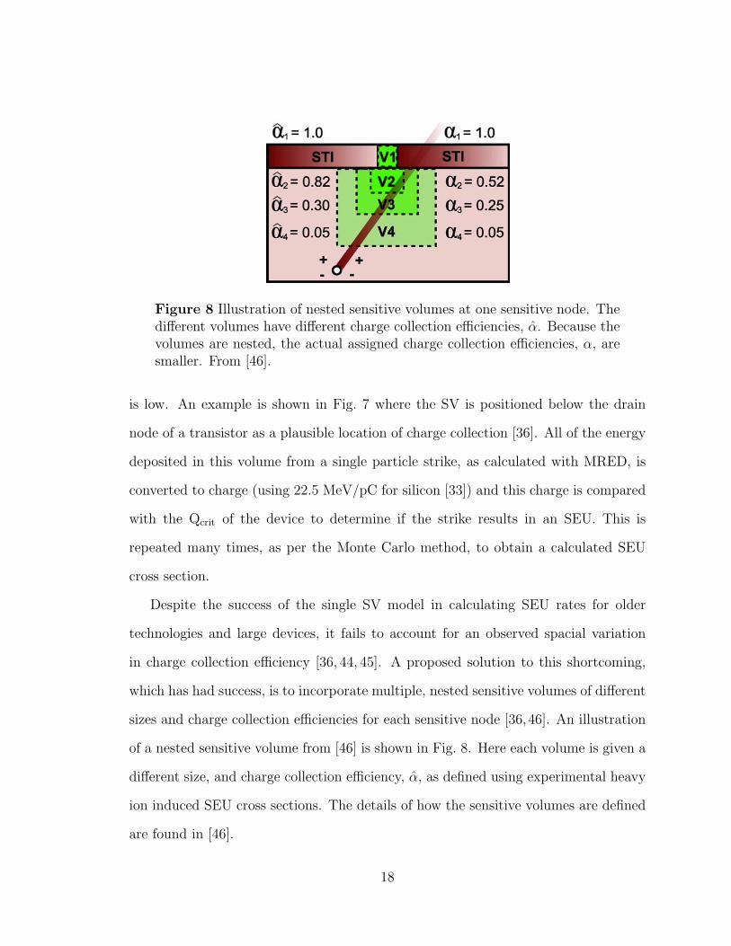
Figure 8 Illustration of nested sensitive volumes at one sensitive node. Thedi↵erent volumes have di↵erent charge collection e�ciencies, ↵̂. Because thevolumes are nested, the actual assigned charge collection e�ciencies, ↵, aresmaller. From [46].
is low. An example is shown in Fig. 7 where the SV is positioned below the drain
node of a transistor as a plausible location of charge collection [36]. All of the energy
deposited in this volume from a single particle strike, as calculated with MRED, is
converted to charge (using 22.5 MeV/pC for silicon [33]) and this charge is compared
with the Qcrit of the device to determine if the strike results in an SEU. This is
repeated many times, as per the Monte Carlo method, to obtain a calculated SEU
cross section.
Despite the success of the single SV model in calculating SEU rates for older
technologies and large devices, it fails to account for an observed spacial variation
in charge collection e�ciency [36, 44, 45]. A proposed solution to this shortcoming,
which has had success, is to incorporate multiple, nested sensitive volumes of di↵erent
sizes and charge collection e�ciencies for each sensitive node [36,46]. An illustration
of a nested sensitive volume from [46] is shown in Fig. 8. Here each volume is given a
di↵erent size, and charge collection e�ciency, ↵̂, as defined using experimental heavy
ion induced SEU cross sections. The details of how the sensitive volumes are defined
are found in [46].
18
In this dissertation, a calibrated nested sensitive volume model of a 65 nm SRAM
is used to perform MRED calculations of SEU cross section. This is done both for
single and multiple bit upset events from a single particle strike. The following section
will describe single and multiple bit upsets.
Single and Multiple Bit Upsets
As technology has scaled down, the size of a device’s SV has, in general, also de-
creased, and the spacing between two sensitive nodes in a device has decreased as
well. Additionally, the Qcrit of devices has decreased. Together, these factors have
increased the probability of an event where a single particle strike can cause su�-
cient charge to be deposited in two or more SVs to cause a coincident upset. These
coincident upsets on multiple SVs are called multiple bit upsets (MBUs) or multiple
cell upsets (MCUs). Although these two terms are sometimes used synonymously,
there is a somewhat subtle, but important, di↵erence between them. A single bit
upset (SBU) occurs when one bit/cell is upset by a single particle strike. An MCU
occurs when multiple bits/cells are upset by a single incident particle. A MBU occurs
when the multiple bits/cells that are upset are in the same data word [24, 47]. Thus
the calculated MCU cross section can be considered a worst-case MBU cross section,
depending on word bit placement. Because a Monte Carlo calculation of an MBU
cross section would necessarily make some assumptions about the word bit placement
of the device (which can vary) all of the calculations done in this work are of MCU
cross sections.
In the past, the term SEU has been used synonymously with SBU because MBU
rates were low, or nonexistent for older technologies. Thus, the terms SBU and SEU
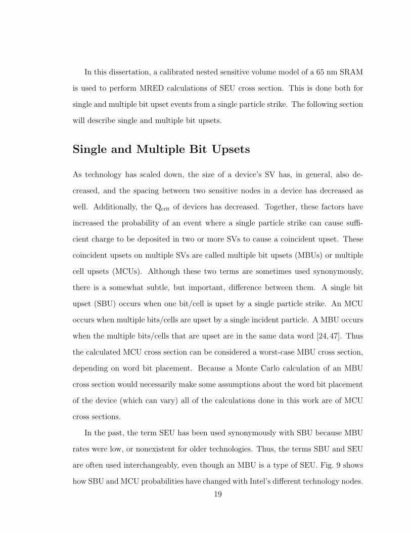
are often used interchangeably, even though an MBU is a type of SEU. Fig. 9 shows
how SBU and MCU probabilities have changed with Intel’s di↵erent technology nodes.
19
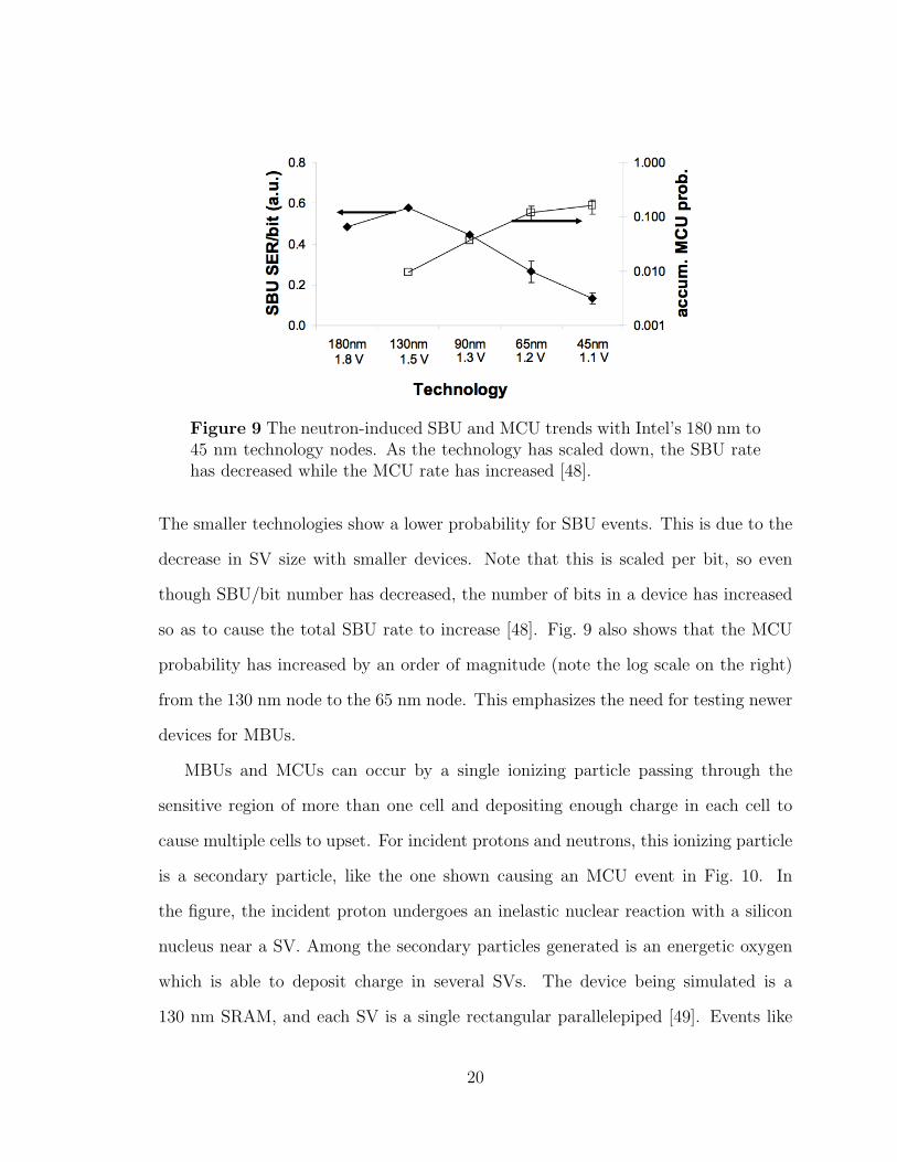
Figure 9 The neutron-induced SBU and MCU trends with Intel’s 180 nm to45 nm technology nodes. As the technology has scaled down, the SBU ratehas decreased while the MCU rate has increased [48].
The smaller technologies show a lower probability for SBU events. This is due to the
decrease in SV size with smaller devices. Note that this is scaled per bit, so even
though SBU/bit number has decreased, the number of bits in a device has increased
so as to cause the total SBU rate to increase [48]. Fig. 9 also shows that the MCU
probability has increased by an order of magnitude (note the log scale on the right)
from the 130 nm node to the 65 nm node. This emphasizes the need for testing newer
devices for MBUs.
MBUs and MCUs can occur by a single ionizing particle passing through the
sensitive region of more than one cell and depositing enough charge in each cell to
cause multiple cells to upset. For incident protons and neutrons, this ionizing particle
is a secondary particle, like the one shown causing an MCU event in Fig. 10. In
the figure, the incident proton undergoes an inelastic nuclear reaction with a silicon
nucleus near a SV. Among the secondary particles generated is an energetic oxygen
which is able to deposit charge in several SVs. The device being simulated is a
130 nm SRAM, and each SV is a single rectangular parallelepiped [49]. Events like
20
Figure 10 Representation of a MCU event in a 130 nm SRAM caused byan oxygen recoil from a proton-silicon nuclear collision. From [49].
the one shown in Fig. 10 illustrate the need to understand nuclear collisions in order
to gain insight into the underlying mechanisms of SEUs, particularly for ones caused
by protons and neutrons. The following section discusses nuclear collisions and their
role in proton- and neutron-induced SEUs.
Proton and Neutron-Induced SEUs - Nuclear Re-
actions
Eq. 1 shows that LET scales with z2, and inversely with �2. Because �2 scales
classically with energy/amu, lower-Z ions and highly energetic ions will have lower
LET values and will thus deposit less charge in materials. However, this does not
mean they can be excluded in SEU studies. Protons, neutrons, and highly energetic
heavy ions can still produce significant upset rates due to indirect interactions. These
particles can undergo inelastic nuclear collisions (see Fig. 11B) with materials in and
surrounding a device, producing heavier and/or less energetic secondary particles
that can have a higher LET than the primary ion [38, 50–53]. Fig. 11 shows charge
deposition from energetic particles as recorded by nuclear photographic emulsions.
21
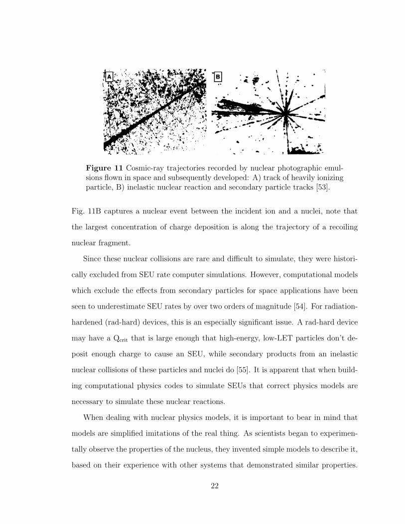
Figure 11 Cosmic-ray trajectories recorded by nuclear photographic emul-sions flown in space and subsequently developed: A) track of heavily ionizingparticle, B) inelastic nuclear reaction and secondary particle tracks [53].
Fig. 11B captures a nuclear event between the incident ion and a nuclei, note that
the largest concentration of charge deposition is along the trajectory of a recoiling
nuclear fragment.
Since these nuclear collisions are rare and di�cult to simulate, they were histori-
cally excluded from SEU rate computer simulations. However, computational models
which exclude the e↵ects from secondary particles for space applications have been
seen to underestimate SEU rates by over two orders of magnitude [54]. For radiation-
hardened (rad-hard) devices, this is an especially significant issue. A rad-hard device
may have a Qcrit that is large enough that high-energy, low-LET particles don’t de-
posit enough charge to cause an SEU, while secondary products from an inelastic
nuclear collisions of these particles and nuclei do [55]. It is apparent that when build-
ing computational physics codes to simulate SEUs that correct physics models are
necessary to simulate these nuclear reactions.
When dealing with nuclear physics models, it is important to bear in mind that
models are simplified imitations of the real thing. As scientists began to experimen-
tally observe the properties of the nucleus, they invented simple models to describe it,
based on their experience with other systems that demonstrated similar properties.
22
For example, the similarities seen between the interaction of protons and neutrons in
the nucleus of an atom and the interactions of atoms in liquids gave rise to the liquid
drop model [56] of the atomic nucleus. As experimental nuclear physics expanded
the knowledge of the nucleus, new models were created to explain the new properties
observed. For example, the shell model [57] of the nucleus.
Because models are not typically created by a rigorous derivation from first prin-
ciples, but rather based on observation and analogy, the understanding that can be
gained from models is often qualitative in nature, particularly when dealing with
many-body problems. Because nuclear reactions can involve a large number of par-
ticles and are extremely complicated in nature, models shall never achieve an exact
solution. A nuclear reaction model is thus a simpler physical system whose prop-
erties we can understand and calculate more easily, and possibly even visualize. It
is a first order approximation to the nuclear system and can be further refined to
make it approach reality [58]. However, it will not be able to reproduce all nuclear
parameters perfectly. This could only be achieved by solving the original quantum
many-body problem, which is too complicated and time consuming even for modern-
day computers. A given nuclear physics model will provide a description of the set of
properties upon which it is based. It cannot assure us an accurate description of other
properties that haven’t been experimentally observed. Thus models are in constant
need of validating, refining and perhaps even merging with alternative models which
accurately describe a separate set of properties.
There exist multiple physics models that have been developed to understand the
nuclear fragmentation process. These models vary in complexity and popularity. The
approach that has been implemented in most current computer simulation models
involves a multiple stage approach with anywhere between two and five di↵erent
stages [59, 60], and are based on experimental observation of particle emissions from
23
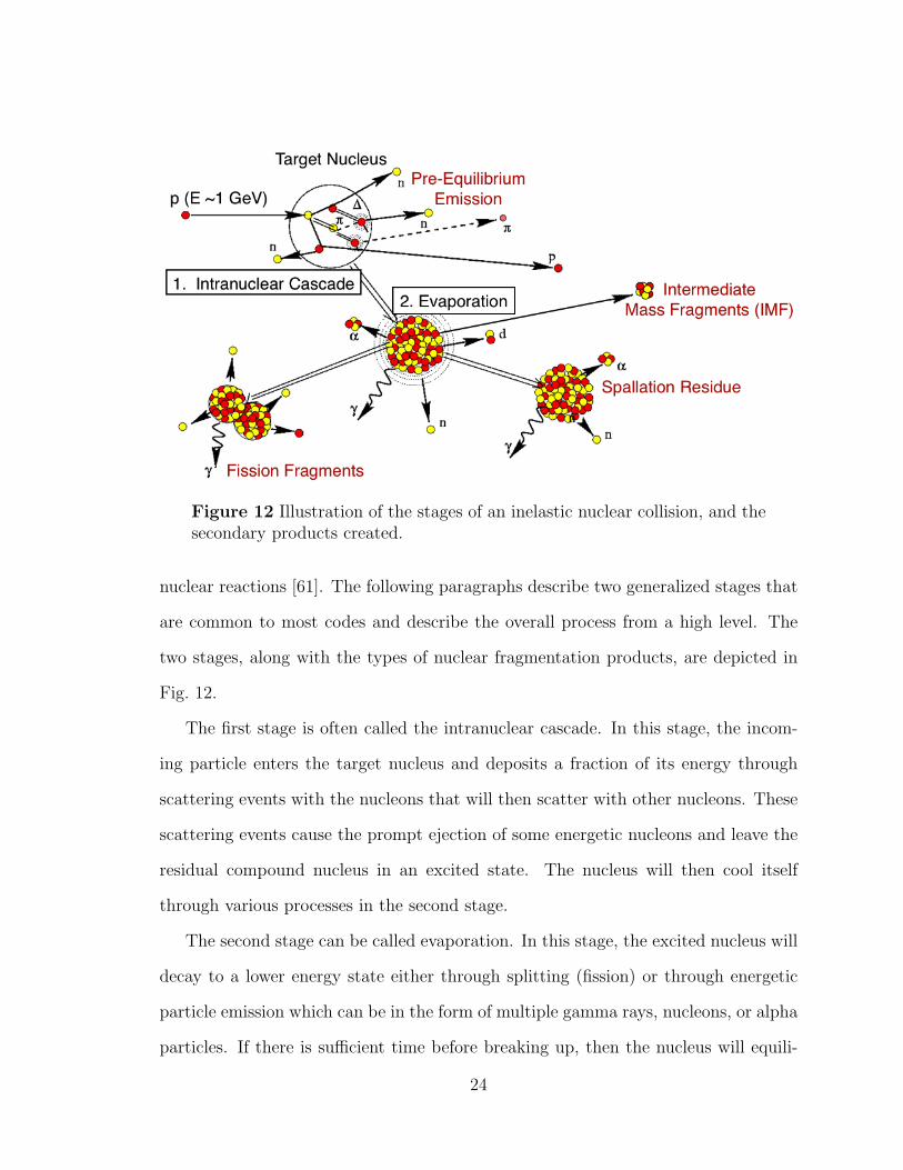
Figure 12 Illustration of the stages of an inelastic nuclear collision, and thesecondary products created.
nuclear reactions [61]. The following paragraphs describe two generalized stages that
are common to most codes and describe the overall process from a high level. The
two stages, along with the types of nuclear fragmentation products, are depicted in
Fig. 12.
The first stage is often called the intranuclear cascade. In this stage, the incom-
ing particle enters the target nucleus and deposits a fraction of its energy through
scattering events with the nucleons that will then scatter with other nucleons. These
scattering events cause the prompt ejection of some energetic nucleons and leave the
residual compound nucleus in an excited state. The nucleus will then cool itself
through various processes in the second stage.
The second stage can be called evaporation. In this stage, the excited nucleus will
decay to a lower energy state either through splitting (fission) or through energetic
particle emission which can be in the form of multiple gamma rays, nucleons, or alpha
particles. If there is su�cient time before breaking up, then the nucleus will equili-
24
brate. Fragments can form in this equilibrated nucleus and repel each other through
the Coulomb interaction leading to IMF products. Once the residual nucleus’s energy
drops below its binding energy, it will decay via pure gamma emission to a stable or
radioactive state, which is the spallation residue.
The secondary products from nuclear reactions which are of most interest from a
radiation e↵ects standpoint can then be classified into three categories [60,62,63]:
1. Spallation - A spallation reaction produces one or more secondary nucleons
and/or light ions as the excited nucleus decays leaving a heavy residual fragment
from the target nucleus. These heavy fragments have a mass typically greater
than or equal to about 2/3 of the target atom mass for incident protons and
neutrons, and often have a comparatively short range and high LET value.
2. Fission - Induced fission productions are only common for very heavy nuclei
(about Z > 65). Fragments have a mass typically about 1/2 of the target
atom mass on average. Because induced fission is an exothermic process, these
fission fragments can have a substantial amount of energy and thus a high range
compared to spallation products. Because of their high mass, they often will
have a high LET value as well.
3. Intermediate Mass Fragmentation (IMF) - IMF products are emitted from
an equilibrated compound nucleus created by the joining of the incident ion and
the target atom. IMF fragments have a mass between about Z = 3 and Z = 20.
IMF production cross section increases with incident particle mass and energy.
A variety of secondary products can be created from inelastic nuclear collisions.
Thus it is essential for a nuclear physics model to come as close to reality as pos-
sible, particularly for proton- and neutron-induced single event upset simulations.
25
An accurate nuclear physics model in a SEU simulation tool not only can allow for
SEU prediction of a device, but can give insight into the mechanisms of SEUs. In
this work, the mechanisms of proton- and neutron-induced SEUs is investigated via
experimental techniques and Monte Carlo simulation using the SEU simulation tool,
MRED. The following chapter details the experiments performed in this work, and
describes how MRED was used.
26
CHAPTER III
EXPERIMENTAL AND SIMULATION
METHODS
This chapter describes the experimental and simulation techniques and devices
used in this study. Details are given of a pulsed height analysis system with an
integrated time of flight measurement capability, which was constructed as part of
this work. A description of the diode structures which were fabricated specifically for
this study is also presented. Finally, the Monte Carlo simulation tool and its use in
this work is described.
Charge collection measurements
For the experiments performed in this work, the amount of deposited charge collected
in a the sensitive volume region of a device due to incident protons and neutrons is
measured and histogrammed. This is accomplished through pulse height analysis
(PHA). This section describes the principles of pulse height analysis and the 16 chan-
nel PHA system which was built for this study to perform the measurements [64].
Pulse height analysis (PHA)
In general, the technique of pulse height analysis (PHA) takes a radiation-induced
current pulse from a detector and converts it to a pulse whose amplitude is propor-
tional to the integrated current, which is equal to the total charge collected in the
detector. The pulse height can then be stored, and many radiation-induced events
27
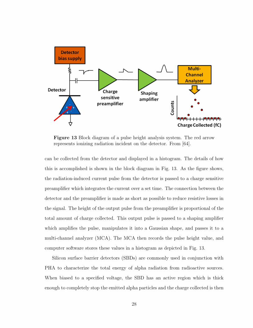
Figure 13 Block diagram of a pulse height analysis system. The red arrowrepresents ionizing radiation incident on the detector. From [64].
can be collected from the detector and displayed in a histogram. The details of how
this is accomplished is shown in the block diagram in Fig. 13. As the figure shows,
the radiation-induced current pulse from the detector is passed to a charge sensitive
preamplifier which integrates the current over a set time. The connection between the
detector and the preamplifier is made as short as possible to reduce resistive losses in
the signal. The height of the output pulse from the preamplifier is proportional of the
total amount of charge collected. This output pulse is passed to a shaping amplifier
which amplifies the pulse, manipulates it into a Gaussian shape, and passes it to a
multi-channel analyzer (MCA). The MCA then records the pulse height value, and
computer software stores these values in a histogram as depicted in Fig. 13.
Silicon surface barrier detectors (SBDs) are commonly used in conjunction with
PHA to characterize the total energy of alpha radiation from radioactive sources.
When biased to a specified voltage, the SBD has an active region which is thick
enough to completely stop the emitted alpha particles and the charge collected is then
28
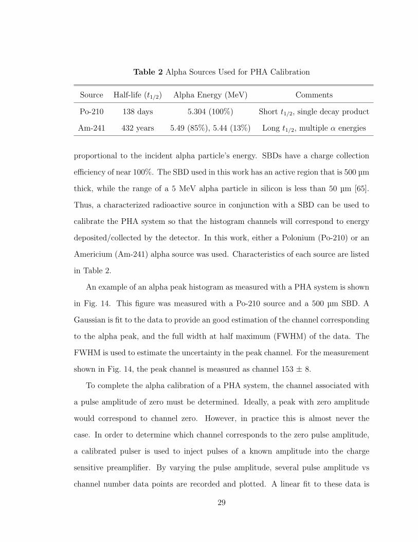
Table 2 Alpha Sources Used for PHA Calibration
Source Half-life (t1/2) Alpha Energy (MeV) Comments
Po-210 138 days 5.304 (100%) Short t1/2, single decay product
Am-241 432 years 5.49 (85%), 5.44 (13%) Long t1/2, multiple ↵ energies
proportional to the incident alpha particle’s energy. SBDs have a charge collection
e�ciency of near 100%. The SBD used in this work has an active region that is 500 µm
thick, while the range of a 5 MeV alpha particle in silicon is less than 50 µm [65].
Thus, a characterized radioactive source in conjunction with a SBD can be used to
calibrate the PHA system so that the histogram channels will correspond to energy
deposited/collected by the detector. In this work, either a Polonium (Po-210) or an
Americium (Am-241) alpha source was used. Characteristics of each source are listed
in Table 2.
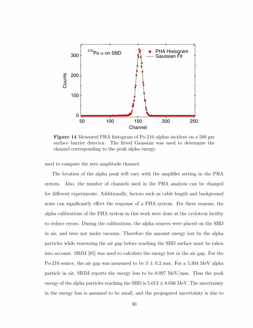
An example of an alpha peak histogram as measured with a PHA system is shown
in Fig. 14. This figure was measured with a Po-210 source and a 500 µm SBD. A
Gaussian is fit to the data to provide an good estimation of the channel corresponding
to the alpha peak, and the full width at half maximum (FWHM) of the data. The
FWHM is used to estimate the uncertainty in the peak channel. For the measurement
shown in Fig. 14, the peak channel is measured as channel 153 ± 8.
To complete the alpha calibration of a PHA system, the channel associated with
a pulse amplitude of zero must be determined. Ideally, a peak with zero amplitude
would correspond to channel zero. However, in practice this is almost never the
case. In order to determine which channel corresponds to the zero pulse amplitude,
a calibrated pulser is used to inject pulses of a known amplitude into the charge
sensitive preamplifier. By varying the pulse amplitude, several pulse amplitude vs
channel number data points are recorded and plotted. A linear fit to these data is
29
300
200
100
0
Cou
nts
25020015010050Channel
PHA Histogram Gaussian Fit
210Po _ on SBD
Figure 14 Measured PHA histogram of Po-210 alphas incident on a 500 µmsurface barrier detector. The fitted Gaussian was used to determine thechannel corresponding to the peak alpha energy.
used to compute the zero amplitude channel.
The location of the alpha peak will vary with the amplifier setting in the PHA
system. Also, the number of channels used in the PHA analysis can be changed
for di↵erent experiments. Additionally, factors such as cable length and background
noise can significantly e↵ect the response of a PHA system. For these reasons, the
alpha calibrations of the PHA system in this work were done at the cyclotron facility
to reduce errors. During the calibrations, the alpha sources were placed on the SBD
in air, and were not under vacuum. Therefore the amount energy lost by the alpha
particles while traversing the air gap before reaching the SBD surface must be taken
into account. SRIM [65] was used to calculate the energy lost in the air gap. For the
Po-210 source, the air gap was measured to be 3 ± 0.2 mm. For a 5.304 MeV alpha
particle in air, SRIM reports the energy loss to be 0.097 MeV/mm. Thus the peak
energy of the alpha particles reaching the SBD is 5.013 ± 0.036 MeV. The uncertainty
in the energy loss is assumed to be small, and the propagated uncertainty is due to
30
the uncertainty in the air gap measurement. Note that the air gap not only increases
the uncertainty in the alpha energy, but also causes the alpha energy peak to broaden
due to straggling [65].
Once the alpha peak and the zero amplitude channels are known, the conversion
from channel number to energy deposited can be calculated for the PHA system. This
is done simply by determining the linear relationship between channel number and
energy, using the two data points. For example, suppose the zero channel was found
to be channel 7, and the channel for the 5.013 ± 0.036 MeV alpha particles was found
to be 153 ± 8, as shown in Fig. 14. The slope of the line determined by these two data
points would be: (5.013�0)/(153�7) = 0.03434 ± 1.81 ⇥ 10�3 MeV/channel. The
uncertainty associated with the energy calibration is greater for higher channel num-
bers. For example, channel 2000 in this example would correspond to 68.7 ± 3.6 MeV.
It is important to take these uncertainties into account when evaluating the data taken
by a PHA system which has used the described method for energy calibration.
Energy deposited in silicon generates charge with a conversion factor of 0.0225 MeV/fC
[33]. The charge collection region of modern semiconducting devices is most often
composed of doped silicon. Thus this factor is commonly used to convert between
deposited energy and charge collected. It is used in this study to convert energy in
the PHA energy calibration to collected charge.
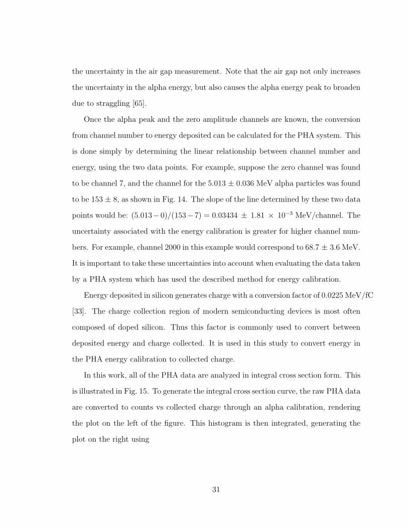
In this work, all of the PHA data are analyzed in integral cross section form. This
is illustrated in Fig. 15. To generate the integral cross section curve, the raw PHA data
are converted to counts vs collected charge through an alpha calibration, rendering
the plot on the left of the figure. This histogram is then integrated, generating the
plot on the right using
31
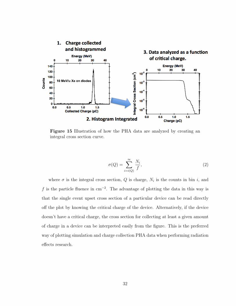
Figure 15 Illustration of how the PHA data are analyzed by creating anintegral cross section curve.
�(Q) =1X
i=i(Q)
Ni
f, (2)
where � is the integral cross section, Q is charge, Ni
is the counts in bin i, and
f is the particle fluence in cm�2. The advantage of plotting the data in this way is
that the single event upset cross section of a particular device can be read directly
o↵ the plot by knowing the critical charge of the device. Alternatively, if the device
doesn’t have a critical charge, the cross section for collecting at least a given amount
of charge in a device can be interpreted easily from the figure. This is the preferred
way of plotting simulation and charge collection PHA data when performing radiation
e↵ects research.
32
16 channel PHA system
In order to allow for parallel data collection with multiple devices, a 16 channel PHA
system was designed an built, in part, for this work. This system has the capability
of performing simultaneous charge collection measurements on up to 16 devices, al-
though for reasons stated below, only 8 devices were tested in parallel in this study.
This parallel data acquisition not only allowed for simultaneous irradiation of di↵er-
ent devices, but also redundant devices for added confidence in the measurements.
This 16 channel PHA system was used for all of the experimental data reported in
this work. Some details of this PHA system are also given in [64], but are listed here
as well for the reader.
A block diagram of the 16 channel PHA system used is shown in Fig. 16. In this 16
channel PHA system, a Mesytec MPRS-16 preamplifier/shaping amplifier is used in
conjunction with the Phillips Scientific 7164H peak sensing analog-to-digital converter
(ADC). The 7164H is a module following the Computer Automated Measurement And
Control (CAMAC) standard, so a CAMAC crate controller is needed to interface with
it. A Kinetic Systems 3988 General Purpose Interface Bus (GPIB) crate controller
was used to interface a computer with the CAMAC crate modules. In order to prevent
the long latency of the GPIB standard from reducing the PHA systems bandwidth, a
Hytec 1342 auxiliary crate controller was used in List Mode. The 1342 stored the PHA
events in a bu↵er, which was periodically read out by the 3988. The software used to
interface and control the CAMAC modules was written by Marcus Mendenhall using
the Python Laboratory Operations Toolkit. This software saves every digitization
event from each of the 16 channels along with a timestamp, which was useful for post
processing of the data.
A discriminator board was designed and built as a custom printed circuit board
33
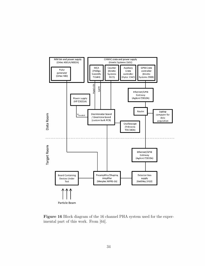
Par$cle(Beam(
Board(Containing(Devices(Under(
Test(
Figure 16 Block diagram of the 16 channel PHA system used for the exper-imental part of this work. From [64].
34
(PCB). The discriminator board detects when a shaped pulse from any of the channels
in the MPRS-16 exceeds an adjustable threshold voltage, and then triggers the 7164H
to digitize the pulse on each channel. The detailed design of the discriminator board
is given in [64]. Note that, once triggered, the 7164H digitizes the signals present
at that moment on all 16 inputs. This increases the dead time of the PHA system.
However, it also allows for the identification of anomalous events that are manifest
as large-amplitude charge collection events a↵ecting multiple channels at the same
time. These events were identified as being caused by noise spikes on the detector
bias supply power line (see Fig. 13). These events were easily identified and removed
from the pulse height spectra through post processing of the data. The dead time
of the system was measured by sampling the BUSY signal of the 7164H at 10 MHz.
The fraction of the time that BUSY was asserted was defined as the dead time, and
was determined using a Kinetic Systems 3615 Counter.
Because of the variability in the response between channels, it is necessary to
perform an energy calibration on each channel on site before device irradiation using
the alpha calibration technique described in the previous section. For the energy
calibration, the SBD was connected to the PCB which held the devices under test,
and biased using the Keithley 2410 power supply shown in Fig. 16. This PCB will be
described in the following section.
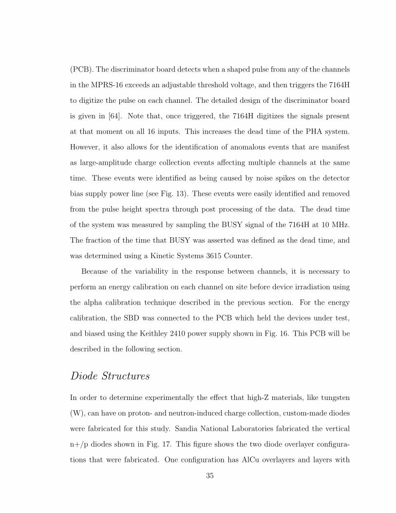
Diode Structures
In order to determine experimentally the e↵ect that high-Z materials, like tungsten
(W), can have on proton- and neutron-induced charge collection, custom-made diodes
were fabricated for this study. Sandia National Laboratories fabricated the vertical
n+/p diodes shown in Fig. 17. This figure shows the two diode overlayer configura-
tions that were fabricated. One configuration has AlCu overlayers and layers with
35
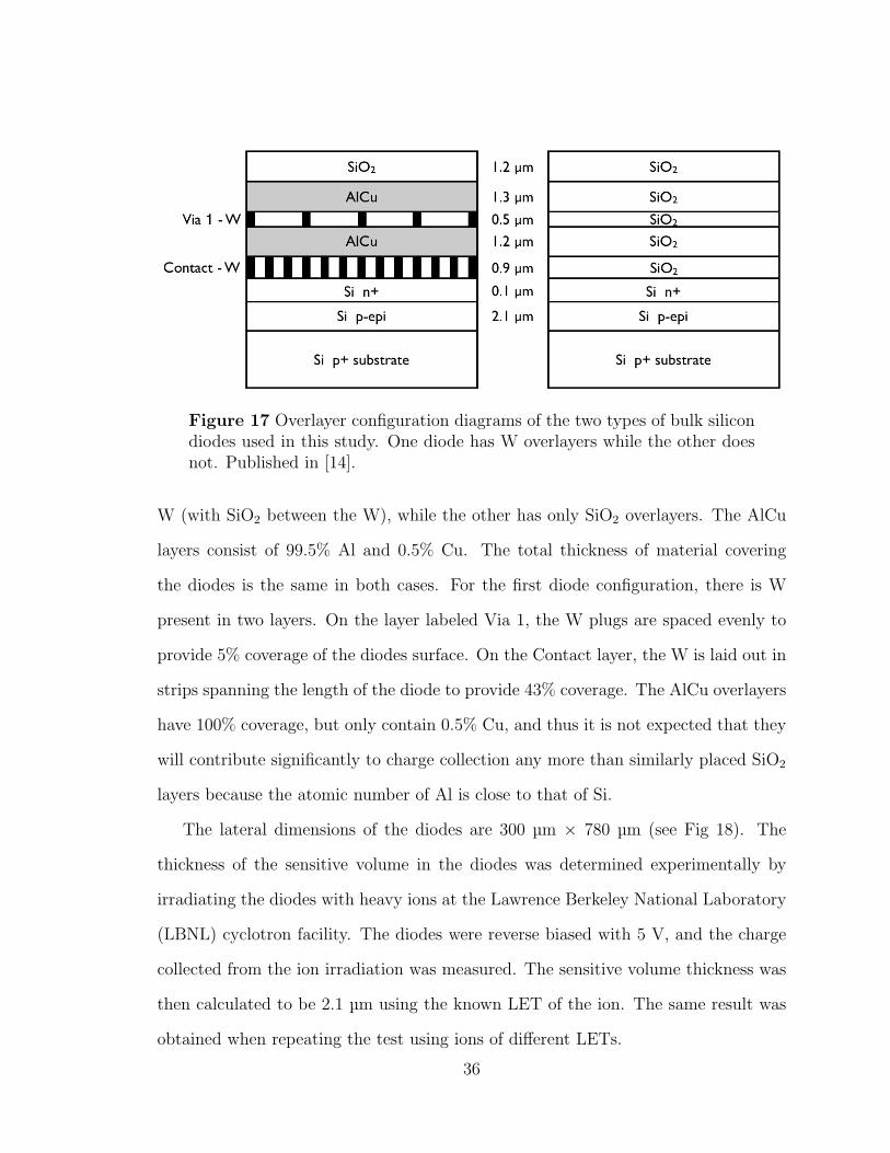
Figure 17 Overlayer configuration diagrams of the two types of bulk silicondiodes used in this study. One diode has W overlayers while the other doesnot. Published in [14].
W (with SiO2 between the W), while the other has only SiO2 overlayers. The AlCu
layers consist of 99.5% Al and 0.5% Cu. The total thickness of material covering
the diodes is the same in both cases. For the first diode configuration, there is W
present in two layers. On the layer labeled Via 1, the W plugs are spaced evenly to
provide 5% coverage of the diodes surface. On the Contact layer, the W is laid out in
strips spanning the length of the diode to provide 43% coverage. The AlCu overlayers
have 100% coverage, but only contain 0.5% Cu, and thus it is not expected that they
will contribute significantly to charge collection any more than similarly placed SiO2
layers because the atomic number of Al is close to that of Si.
The lateral dimensions of the diodes are 300 µm ⇥ 780 µm (see Fig 18). The
thickness of the sensitive volume in the diodes was determined experimentally by
irradiating the diodes with heavy ions at the Lawrence Berkeley National Laboratory
(LBNL) cyclotron facility. The diodes were reverse biased with 5 V, and the charge
collected from the ion irradiation was measured. The sensitive volume thickness was
then calculated to be 2.1 µm using the known LET of the ion. The same result was
obtained when repeating the test using ions of di↵erent LETs.
36
W SiO2
780 µm
300 µm
Figure 18 A top-down view of a pair of diodes with the two overlayer con-figurations as they were fabricated.
Initial Monte Carlo simulations using the dimensions shown in Fig. 17 for the sen-
sitive volume region revealed that the placement of the sensitive volume region with
respect to the W overlayers significantly a↵ected the calculated charge deposition.
For this reason, doping profile measurements were made on the diodes via destruc-
tive analysis and 2-D technology computer-aided design (TCAD) simulations were
performed to better understand the location and dimensions of the charge collection
region. The simulated diode structure replicated the doping profiles and geometries
of the n+, p-epi and p+ substrate regions of the diodes. Heavy ion strikes emulating
the linear energy transfer (LET) of those used in the LBNL experiments were used to
strike the n+ region of the diode. Current transients were measured at the n+ region
contacts, which were then integrated over the duration of the simulation to get the
total collected charge for a given ion strike. Device physics models activated in the
simulations were: Poisson and Fermi-Dirac statistics, Shockley-Reed-Hall and Auger
recombination, and dopant-dependent mobility models. All simulations were carried
out at room temperature settings. The TCAD simulations were done by Vishwa
Ramachandran.
The TCAD simulations showed that, under a 5 V bias, the depletion region only
extends 1.2 µm into the epitaxial layer, however, charge deposited throughout the
2.1 µm thick layer is collected. This type of charge collection from an epitaxial layer
37
is consistent with [66]. TCAD simulations that stopped the incident ion at the top
edge of the p-epi region shown in Fig. 17 revealed that charge collection from the
n+ region is negligible. Therefore, for the Monte Carlo simulations performed in this
work, the 2.1 µm thick sensitive volumes of the diodes are placed directly below the
n+ silicon region.
These test structures are unique in that they allow for isolating the influence of
W overlayers on charge collection, and also provide structures with a well-defined
sensitive volume region for Monte Carlo simulation comparison. The diodes rela-
tively large cross sectional area allows for more frequent detection of the proton-
or neutron-induced nuclear reaction events, and thus provides better statistics over
short exposure times. Also, the inclusion of larger-than-typical amounts of W in the
diode overlayers was intentional in order to make their role in charge collection more
observable than they would be in a typical device.
The diodes were fabricated in pairs with the two diode overlayer configurations
adjacent to each other as shown in Fig. 18. The diode pairs were mounted and
bonded out in 40 pin dual in-line packages (DIPs), with each DIP containing two
pairs of diodes. Only four diodes were mounted in each DIP due to the size of the
diodes. Custom PCBs which were designed to be integrated into the 16 channel PHA
system were used to mount the diodes in the beamline for the experiments. These
PCBs were designed to connect 8 channels to each of the 40 pin DIP sockets. Since
only four diodes were mounted in each DIP, only 8 out of the 16 channels were utilized
at a given time for the charge collection experiments.
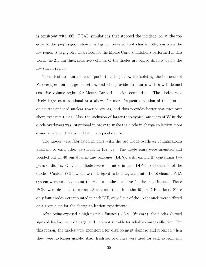
After being exposed a high particle fluence (⇠ 3⇥ 1013 cm-2), the diodes showed
signs of displacement damage, and were not suitable for reliable charge collection. For
this reason, the diodes were monitored for displacement damage and replaced when
they were no longer usable. Also, fresh set of diodes were used for each experiment.
38
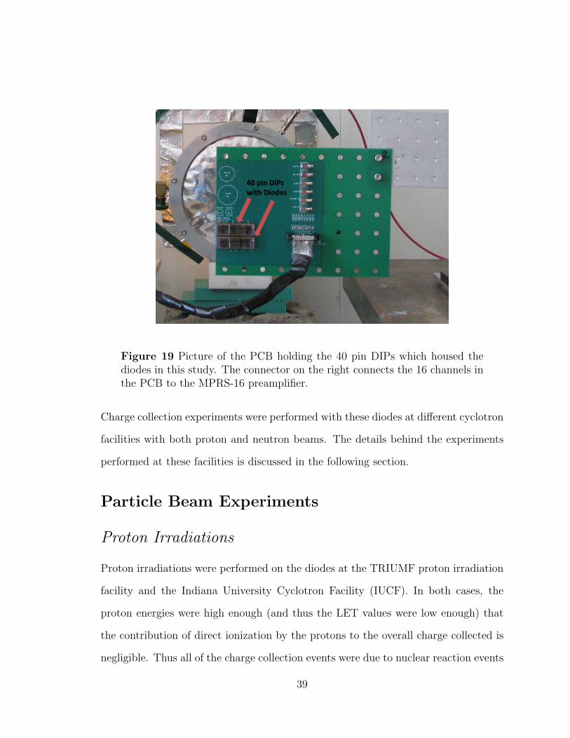
Par$cle(Beam(
Board(Containing(Devices(Under(
Test(
Figure 19 Picture of the PCB holding the 40 pin DIPs which housed thediodes in this study. The connector on the right connects the 16 channels inthe PCB to the MPRS-16 preamplifier.
Charge collection experiments were performed with these diodes at di↵erent cyclotron
facilities with both proton and neutron beams. The details behind the experiments
performed at these facilities is discussed in the following section.
Particle Beam Experiments
Proton Irradiations
Proton irradiations were performed on the diodes at the TRIUMF proton irradiation
facility and the Indiana University Cyclotron Facility (IUCF). In both cases, the
proton energies were high enough (and thus the LET values were low enough) that
the contribution of direct ionization by the protons to the overall charge collected is
negligible. Thus all of the charge collection events were due to nuclear reaction events
39
between a proton and a nucleus from the material in or surrounding the sensitive
volume. Because the cross section for proton-induced nuclear reactions is small, the
devices were exposed to a minimum fluence of 5 ⇥1012 cm-2 for each run in order to
obtain statistically significant data.
Irradiations were performed at TRIUMF using the 500 MeV beamline. Irra-
diations were performed at TRIUMF at 0°(normal incidence), 180°(backside) and
⇠85°(grazing). The IUCF irradiations were all performed at normal incidence. Sev-
eral proton energies were used at IUCF. The highest proton energy available is
198 MeV. Lower proton energy can be obtained by inserting copper degraders be-
tween the end of the beamline and the diodes. However, this does increase the
FWHM of the energy peak due to straggling. In this work, proton energies of 198,
90, 55 and 27 MeV were used. Due to the similarity of the charge collection curves for
90, 55 and 27 MeV energies, only the results from the 90 MeV protons is presented
in this document. The FWHM of the 198 and 90 MeV proton energy peaks are 1.2
and 2.5 MeV respectively.
Neutron Irradiations
Neutron irradiations were performed on the diodes at the Weapons Neutron Research
(WNR) facility at Los Alamos National Laboratory using the Target 4 Flight Path
15L (T4FP15L). This flight path is di↵erent from the ICE House (Irradiation of Chips
and Electronics), flight path 30L, which is commonly used to simulate the terrestrial
neutron environment for radiation e↵ects research. However, the neutron energy
spectrum of this flight path is similar, with a slightly higher flux of the higher energy
neutrons (see Fig. 20). In many radiation e↵ects publications, the ICE House neutron
spectrum is referred to as the WNR neutron spectrum, so this nomenclature is used
here as well.
40
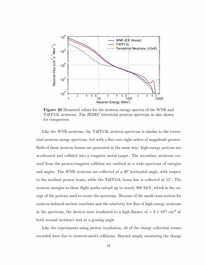
Figure 20 Measured values for the neutron energy spectra of the WNR andT4FP15L neutrons. The JEDEC terrestrial neutron spectrum in also shownfor comparison.
Like the WNR neutrons, the T4FP15L neutron spectrum is similar to the terres-
trial neutron energy spectrum, but with a flux over eight orders of magnitude greater.
Both of these neutron beams are generated in the same way: high-energy protons are
accelerated and collided into a tungsten metal target. The secondary neutrons cre-
ated from the proton-tungsten collision are emitted at a wide spectrum of energies
and angles. The WNR neutrons are collected at a 30° horizontal angle, with respect
to the incident proton beam, while the T4FP15L beam line is collected at 15°. The
neutron energies in these flight paths extend up to nearly 800 MeV, which is the en-
ergy of the protons used to create the spectrum. Because of the small cross section for
neutron-induced nuclear reactions and the relatively low flux of high energy neutrons
in the spectrum, the devices were irradiated to a high fluence of ⇠ 3 ⇥ 1012 cm-2 at
both normal incidence and at a grazing angle.
Like the experiments using proton irradiation, all of the charge collection events
recorded were due to neutron-nuclei collisions. Beyond simply measuring the charge
41
collected due to irradiation by a wide range of neutron energies, insight into the charge
collection mechanism was obtained by correlating a charge collection event with the
incident neutron energy which caused the event. This was accomplished with time of
flight measurements. The following section discusses the time of flight measurements
performed in this work with the neutrons in the T4FP15L beam line.
Time of Flight (TOF) Measurements
For the neutron irradiations done at the WNR facility, a time of flight (TOF) mea-
surement capability was integrated into the 16 channel PHA system. The facility at
WNR provided a pulse signaling the collision of the proton beam with the tungsten
target, generating the neutron beam. This allowed the time between the neutron
generation and a charge collection event to be measured. Using the measured TOF,
the neutron energy is calculated for the neutron whose nuclear collision caused the
measured charge collection in the diode structure. So for each charge collection event,
a corresponding neutron energy is recorded. This section discusses the experimental
details of the TOF setup, the energy calculation, and the limitations in the TOF
measurements.
Description of TOF setup
Because only 4 diodes were bonded out into each DIP as described in Section III,
only 8 of the 16 available channels were used for charge collection measurements.
The TOF measurements were then made by passing the signal from an Ortec 566
time-to-amplitude converter (TAC) to an unused channel in the PHA system. The
output from the TAC was connected directly to one of the channels in the discrim-
inator board (see Fig. 16), with the trigger disabled on that channel. So for every
charge collection event exceeding a given threshold, the MCA would also record a
42
corresponding pulse height from the TAC, but pulses from the TAC would never
trigger the MCA. The start pulse for the TAC is provided by the facility signaling
the time of the neutron generation. The stop pulse for the TAC was retrieved from
the NIM output of the Mesytec MPRS-16 preamplifier/shaping amplifier used for the
charge collection measurement. The amplitude of the pulse from the TAC is then
proportional to the time between neutron generation and the charge collection event.
The TAC was calibrated by connecting a pulser to the start input, while the same
signal was sent to the stop input through a cable of known delay time. The original
time window for pulse measurement on the discriminator board was 1.5 µs, while
the TAC’s full range of time measurement was 2 µs. In order to measure the full
range of time pulses from the TAC, the capacitor on the discriminator board’s timer
was changed to extend the time window for pulse measurement to 6 µs. Because the
charge collection events from the neutron beam were observed every 5-10 seconds, this
extended time window didn’t cause any deadtime or pileup problems. The calibrated
TAC had a measured bin width of 0.62 ns/channel.
Because neutrons cause charge deposition through secondary particles from nu-
clear collisions, the TOF measured includes the time after a neutron-nucleus collision,
the emission of secondary particles, and the collection of charge deposited by one or
more secondary particle. The time scale of these events is estimated to be less than
a nanosecond, and thus the e↵ect that these events have in delaying the second time
signal is considered negligible.
TOF Calculation
The setup described above is capable of measuring the time between the creation of
each neutron and the charge collection event. For the analysis of these data, it is
necessary to relate that time of flight with a particle energy with a TOF equation.
43
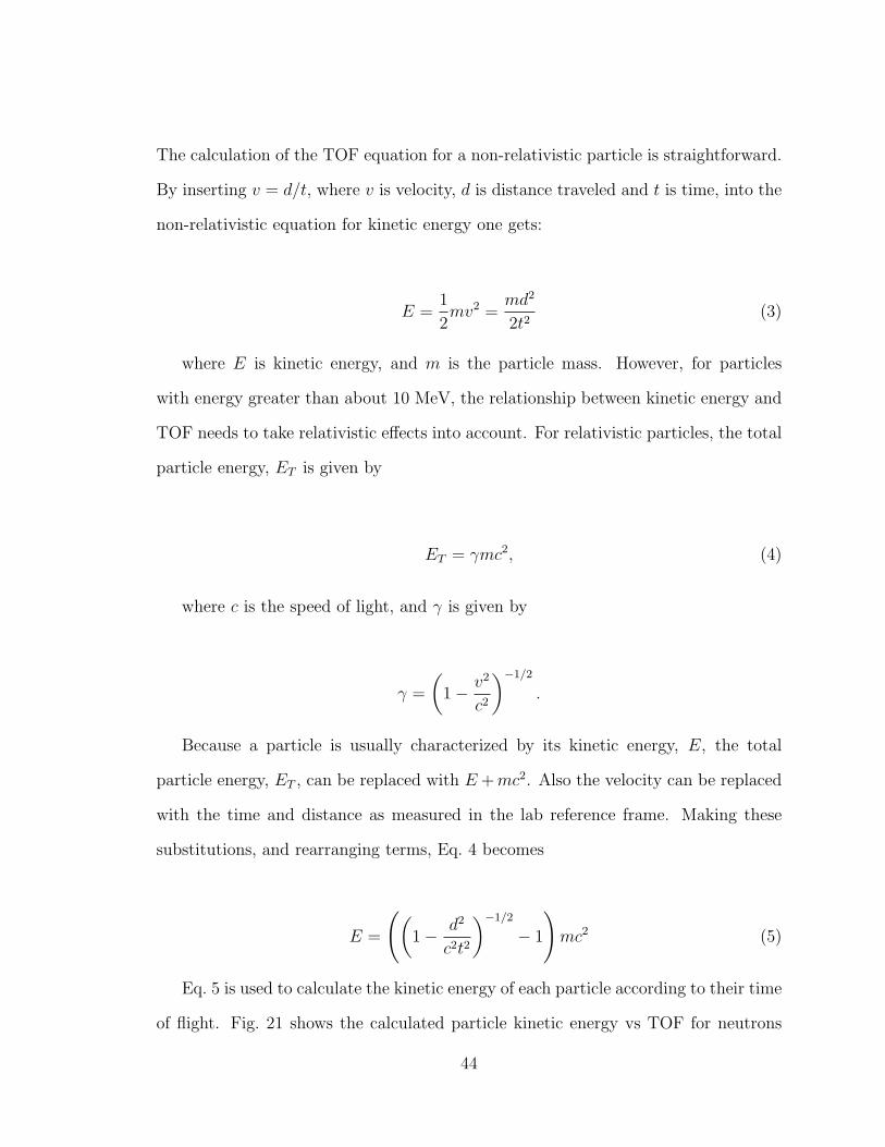
The calculation of the TOF equation for a non-relativistic particle is straightforward.
By inserting v = d/t, where v is velocity, d is distance traveled and t is time, into the
non-relativistic equation for kinetic energy one gets:
E =1
2mv2 =
md2
2t2(3)
where E is kinetic energy, and m is the particle mass. However, for particles
with energy greater than about 10 MeV, the relationship between kinetic energy and
TOF needs to take relativistic e↵ects into account. For relativistic particles, the total
particle energy, ET
is given by
ET
= �mc2, (4)
where c is the speed of light, and � is given by
� =
✓1� v2
c2
◆�1/2
.
Because a particle is usually characterized by its kinetic energy, E, the total
particle energy, ET
, can be replaced with E + mc2. Also the velocity can be replaced
with the time and distance as measured in the lab reference frame. Making these
substitutions, and rearranging terms, Eq. 4 becomes
E =
✓1� d2
c2t2
◆�1/2
� 1
!mc2 (5)
Eq. 5 is used to calculate the kinetic energy of each particle according to their time
of flight. Fig. 21 shows the calculated particle kinetic energy vs TOF for neutrons
44
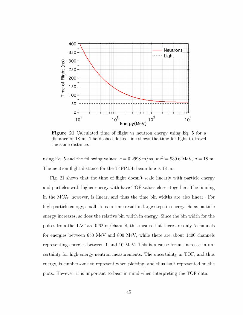
Figure 21 Calculated time of flight vs neutron energy using Eq. 5 for adistance of 18 m. The dashed dotted line shows the time for light to travelthe same distance.
using Eq. 5 and the following values: c = 0.2998 m/ns, mc2 = 939.6 MeV, d = 18 m.
The neutron flight distance for the T4FP15L beam line is 18 m.
Fig. 21 shows that the time of flight doesn’t scale linearly with particle energy
and particles with higher energy with have TOF values closer together. The binning
in the MCA, however, is linear, and thus the time bin widths are also linear. For
high particle energy, small steps in time result in large steps in energy. So as particle
energy increases, so does the relative bin width in energy. Since the bin width for the
pulses from the TAC are 0.62 ns/channel, this means that there are only 5 channels
for energies between 650 MeV and 800 MeV, while there are about 1400 channels
representing energies between 1 and 10 MeV. This is a cause for an increase in un-
certainty for high energy neutron measurements. The uncertainty in TOF, and thus
energy, is cumbersome to represent when plotting, and thus isn’t represented on the
plots. However, it is important to bear in mind when interpreting the TOF data.
45
Monte Carlo Simulations
This section includes a description of the Monte Carlo simulation tool used, as well
as how it was used in this work. A description of the simulations run as a part of this
work is also described. Finally, a list of the available nuclear physics models for the
simulations is given.
Description of Simulation Tool
Various Monte Carlo transport codes exist and are used by di↵erent research groups
in radiation e↵ect research. At Vanderbilt University, a Geant4-based [67] simulation
tool called MRED (Monte Carlo Radiative Energy Deposition) has been developed
for SEE computer simulations. MRED uses a comprehensive set of physics models
from Geant4 for the transport of radiation through matter, and associated energy
deposition. Geant4 is a library of c++ classes that was created and is maintained by
a large international collaboration [67].
MRED is unique in that it extends basic Geant4 capabilities to include additional
nuclear physics models not available in Geant4, novel cross section biasing techniques
for variance reduction [68], and several other useful tools pertinent to SEE prediction
[43]. In MRED, the nuclear physics model desired can be selected at runtime so that
a comparison of the nuclear physics codes is possible while using the same particle
transport and energy deposition routines. Interfacing with MRED is done via Python
scripts.
Monte Carlo simulations are invaluable in radiation e↵ects research due to their
potential of realistically simulating the space environment, the device structure, and
the physics of electronic and nuclear interactions between radiated particles and mat-
ter. To this end, great importance is placed on the correctness of the computational
46
physics used in these simulations, and also on understanding their limitations.
Uses of Simulation Tool
MRED can be used in two di↵erent modes for di↵erent purposes. These are referred
to in this document as “standard mode” and “single event mode”. In the either mode,
MRED is used to simulate the irradiation of a defined 3D structure with one or more
sensitive volumes. The user specifies radiation type, energy and angle of incidence and
location on the structure. The particle can be simulated from all angles, where then
the angle is chosen randomly for each particle. The incident particles are transported,
one at a time, through the 3D structure and tracked, as are any secondary particle
that are generated, and the calculated energy that is deposited in each sensitive
volume (SV) is recorded.
In standard mode, the user specifies how many incident particles are desired and
energy deposited in the SV is recorded in a weighted histogram. This weighted
histogram takes factors such as cross section biasing and geometry into consideration
for easy conversion from a weighted histogram to a cross section curve. For each run,
MRED reports a “fluence unit” variable which is used in place of fluence in Eq. 2 to
create an integral cross section curve.
An example Python script that uses MRED in standard mode is given in Ap-
pendix B. This code runs in MRED version 9.2.0. This example script was used in
this work to simulate proton radiation incident on the pair of diodes described in
section III. The incident protons are randomized over the surface of the diodes at the
specified angle of incidence, simulating the proton beamlines at TRIUMF and IU.
In single event mode, the user has access to all of the information about the
incident particle’s track, as well as any secondary particles which are created. Single
event mode can be used for various purposes. In this work it was used for replaying an
47
event by giving MRED the known random seeds, checking events for a nuclear collision
to gain information about secondary particles, and generating custom histograms to
save multiple cell upset (MCU) information.
An example Python script that uses MRED in single event mode is given in
Appendix C. This code also runs in MRED version 9.2.0. This script defines a 32⇥32
bit array of nested SVs to simulate an SRAM. The nested SV size, charge collection
e�ciency and spacing were calibrated to simulate a 4 Mbit Texas Instruments SRAM
fabricated in a commercial 65 nm Bulk CMOS process. The SV information was
provided by Brian Sierawski. The script runs MRED in single event mode and for
each particle strike, it saves the amount of charge that was deposited in each SV,
along with the weight and random seeds for that event. The data was post-processed
to obtain SEU and MCU cross sections for the device when irradiated by di↵erent
neutron energy spectra. The script was also used to replay events of interest for this
work.
Nuclear Physics Models
As stated above, MRED allows the user to choose from various available physics mod-
els at runtime. There is a di↵erent set of physics models used for simulations done for
hadrons and for heavy ions. In this work, only the hadronic nuclear physics models
are considered since all of the simulations were done with protons or neutrons. Be-
cause the conclusions drawn from the simulations rely heavily on the nuclear physics
model used, a validation was done using the experimental data collected in this work,
as well as nuclear physics experiments not discussed in this document (see [69, 70]).
These validations are done in addition to the many validations and checks that are
performed by the authors of each physics model [67, 71–73]. Table 3 shows a list of
the available physics models in MRED.
48
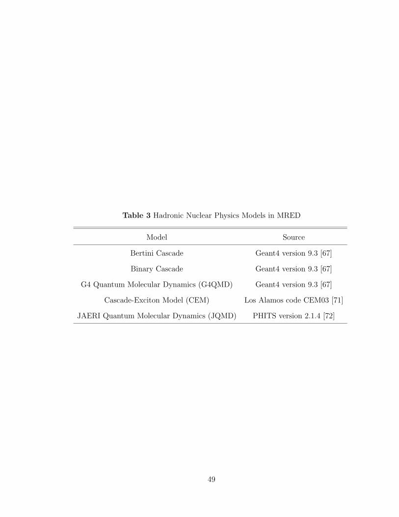
Table 3 Hadronic Nuclear Physics Models in MRED
Model Source
Bertini Cascade Geant4 version 9.3 [67]
Binary Cascade Geant4 version 9.3 [67]
G4 Quantum Molecular Dynamics (G4QMD) Geant4 version 9.3 [67]
Cascade-Exciton Model (CEM) Los Alamos code CEM03 [71]
JAERI Quantum Molecular Dynamics (JQMD) PHITS version 2.1.4 [72]
49
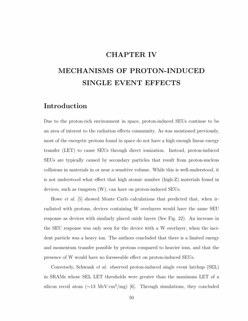
CHAPTER IV
MECHANISMS OF PROTON-INDUCED
SINGLE EVENT EFFECTS
Introduction
Due to the proton-rich environment in space, proton-induced SEUs continue to be
an area of interest to the radiation e↵ects community. As was mentioned previously,
most of the energetic protons found in space do not have a high enough linear energy
transfer (LET) to cause SEUs through direct ionization. Instead, proton-induced
SEUs are typically caused by secondary particles that result from proton-nucleus
collisions in materials in or near a sensitive volume. While this is well-understood, it
is not understood what e↵ect that high atomic number (high-Z) materials found in
devices, such as tungsten (W), can have on proton-induced SEUs.
Howe et al. [5] showed Monte Carlo calculations that predicted that, when ir-
radiated with protons, devices containing W overlayers would have the same SEU
response as devices with similarly placed oxide layers (See Fig. 22). An increase in
the SEU response was only seen for the device with a W overlayer, when the inci-
dent particle was a heavy ion. The authors concluded that there is a limited energy
and momentum transfer possible by protons compared to heavier ions, and that the
presence of W would have no foreseeable e↵ect on proton-induced SEUs.
Conversely, Schwank et al. observed proton-induced single event latchup (SEL)
in SRAMs whose SEL LET thresholds were greater than the maximum LET of a
silicon recoil atom (⇠13 MeV·cm2/mg) [6]. Through simulations, they concluded
50
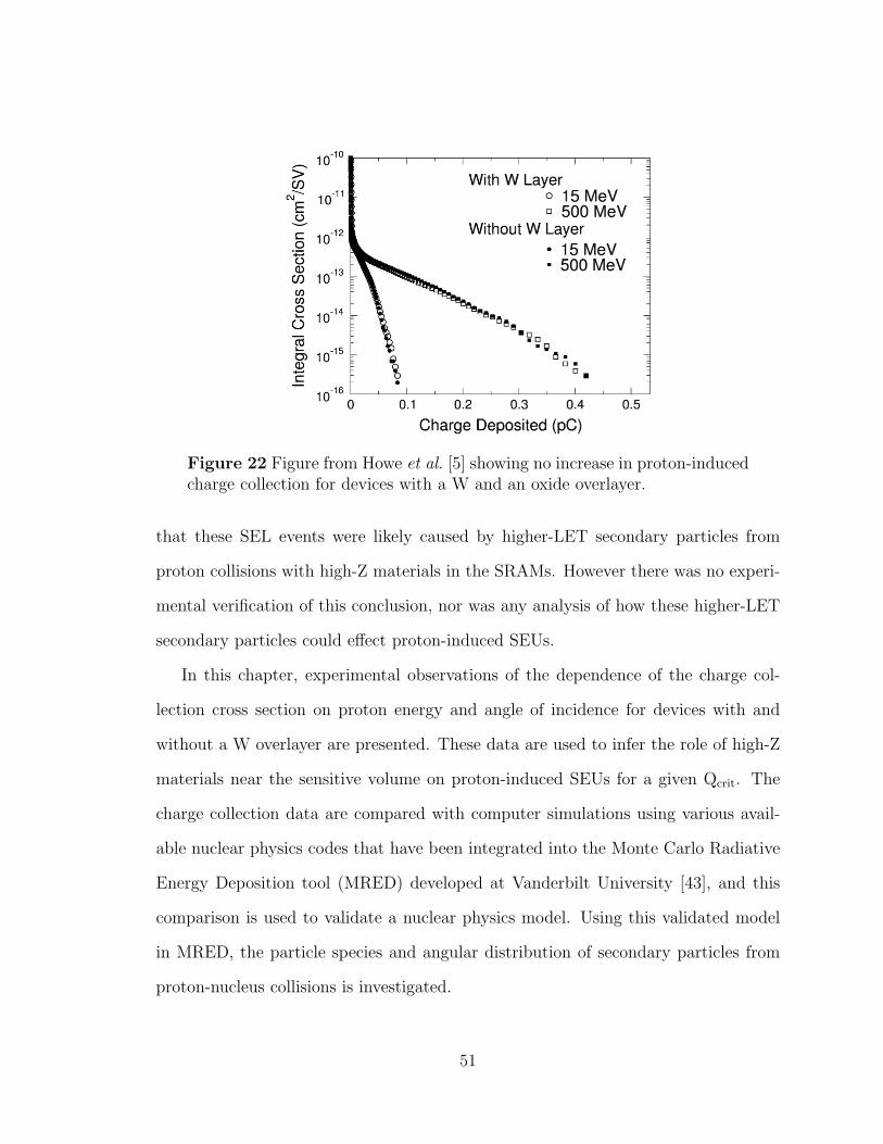
Figure 22 Figure from Howe et al. [5] showing no increase in proton-inducedcharge collection for devices with a W and an oxide overlayer.
that these SEL events were likely caused by higher-LET secondary particles from
proton collisions with high-Z materials in the SRAMs. However there was no experi-
mental verification of this conclusion, nor was any analysis of how these higher-LET
secondary particles could e↵ect proton-induced SEUs.
In this chapter, experimental observations of the dependence of the charge col-
lection cross section on proton energy and angle of incidence for devices with and
without a W overlayer are presented. These data are used to infer the role of high-Z
materials near the sensitive volume on proton-induced SEUs for a given Qcrit. The
charge collection data are compared with computer simulations using various avail-
able nuclear physics codes that have been integrated into the Monte Carlo Radiative
Energy Deposition tool (MRED) developed at Vanderbilt University [43], and this
comparison is used to validate a nuclear physics model. Using this validated model
in MRED, the particle species and angular distribution of secondary particles from
proton-nucleus collisions is investigated.
51
10-12
10-11
10-10
10-9
Inte
gral
Cro
ss S
ectio
n (c
m2 )
40302010 Energy (MeV)
2.01.51.00.5Collected Charge (pC)
90 MeV
200 MeV
500 MeV W overlayers SiO2 overlayers
Figure 23 Measured integral charge collection cross sections for both diodeconfigurations with normally incident 90, 200, and 500 MeV protons. Pub-lished in [14].
Charge Collection Measurements
The results of normally incident 90, 200 and 500 MeV proton irradiations on the
diode structures discussed in section III are shown in integral cross section form in
Fig. 23. The integral cross section is proportional to the probability that the collected
charge exceeds the charge value shown on the x-axis. Displaying the data in this form
is useful because it allows the charge collection cross section to be read directly from
the curve for a given amount of minimum charge collected, Qmin. That is, it is the
cross section for collecting at least that given amount of charge. In this way, the
dependence of the charge collection cross section on proton energy and angle can be
analyzed as a function of minimum charge collected. This charge collection cross
section is analogous to the SEU cross section of a device with the same sensitive
volume dimensions. The SEU cross section could then be read from the cross section
52
plots for a given critical charge. It is important to note that the quantitative SEU
cross section found in this way is only accurate for devices with a sensitive volume
geometry equal to that of the diodes used in this experiment. However, a qualitative
understanding of the proton-induced SEU cross section can be obtained with these
data.
As is seen in Fig. 23, the charge collection cross section increases with proton
energy for the diodes with SiO2 overlayers for any Qmin. This is possibly due to an
increased energy (and thus range) of the high-LET secondary particles. Fig. 23 also
shows that, for 200 and 500 MeV protons, the presence of W near the sensitive volume
region of a device causes a significant increase in the cross section for charge collection
events above ⇠0.5 pC. This e↵ect is even more pronounced for higher charge.
Fig. 23 shows that the impact of the W overlayer strongly depends on the energy
of the incident proton. While the data for the di↵erent diode configurations diverge at
cross sections below about 10-10 cm2 for 200 and 500 MeV protons, a similar divergence
is not seen for the 90 MeV protons until about 10-11 cm2, and the di↵erence between
the two curves after the divergence is minor. Schwank et al. [6] showed through
computer simulation that a probable cause for high-LET secondaries from a proton-
W collision is proton-induced fission. Fig. 23 is consistent with that hypothesis since
the experimental proton-induced fission cross section for W reported in [62] is <1 mb
for proton energies below 100 MeV and increases rapidly to ⇠4 mb at 200 MeV and
⇠10 mb at 500 MeV (see Fig. 24).
There is a significant di↵erence between secondary particles that originate from
proton-induced fission and those that originate from proton-induced spallation. Proton-
induced spallation fragments consist of one or more energetic nucleons and/or light
ion fragments, which typically have a long range and a low LET, and an energetic
residual nucleus, which typically has a high mass number (and thus high LET) but
53
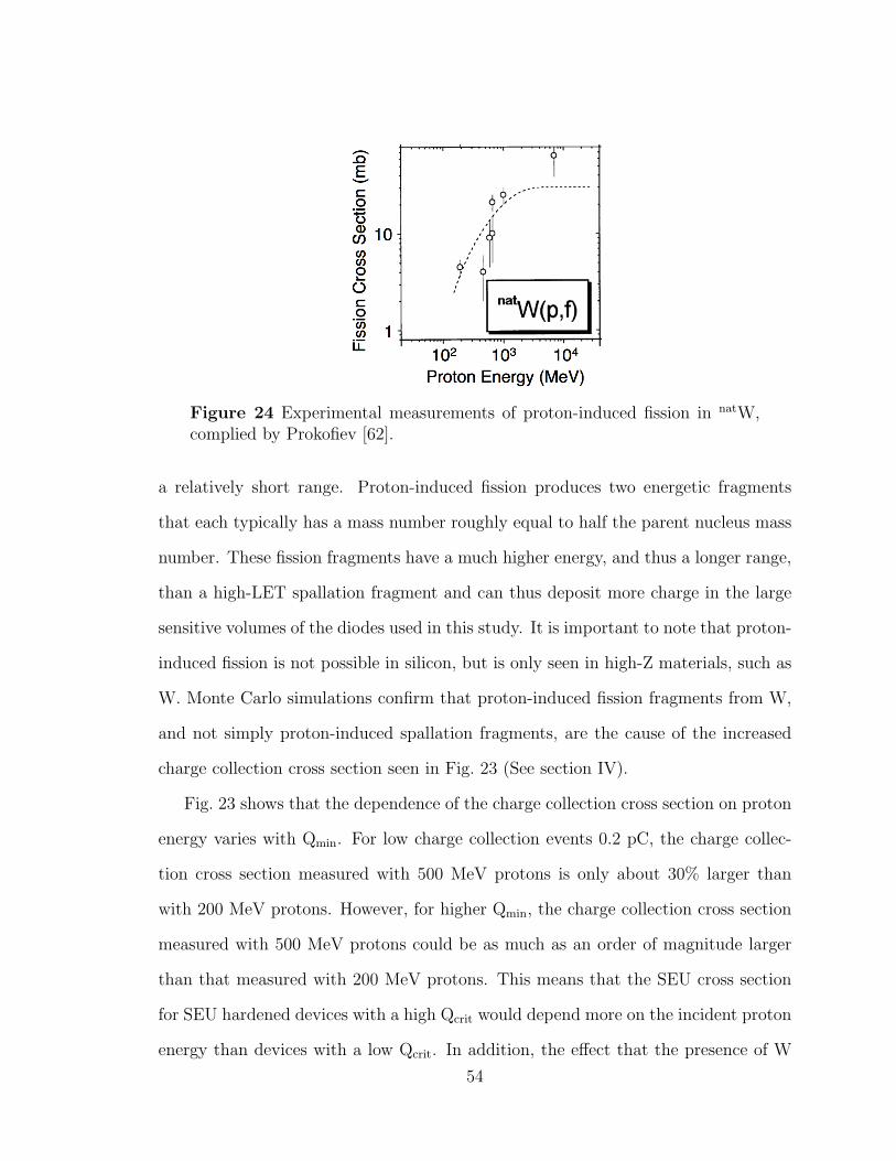
Figure 24 Experimental measurements of proton-induced fission in natW,complied by Prokofiev [62].
a relatively short range. Proton-induced fission produces two energetic fragments
that each typically has a mass number roughly equal to half the parent nucleus mass
number. These fission fragments have a much higher energy, and thus a longer range,
than a high-LET spallation fragment and can thus deposit more charge in the large
sensitive volumes of the diodes used in this study. It is important to note that proton-
induced fission is not possible in silicon, but is only seen in high-Z materials, such as
W. Monte Carlo simulations confirm that proton-induced fission fragments from W,
and not simply proton-induced spallation fragments, are the cause of the increased
charge collection cross section seen in Fig. 23 (See section IV).
Fig. 23 shows that the dependence of the charge collection cross section on proton
energy varies with Qmin. For low charge collection events 0.2 pC, the charge collec-
tion cross section measured with 500 MeV protons is only about 30% larger than
with 200 MeV protons. However, for higher Qmin, the charge collection cross section
measured with 500 MeV protons could be as much as an order of magnitude larger
than that measured with 200 MeV protons. This means that the SEU cross section
for SEU hardened devices with a high Qcrit would depend more on the incident proton
energy than devices with a low Qcrit. In addition, the e↵ect that the presence of W
54
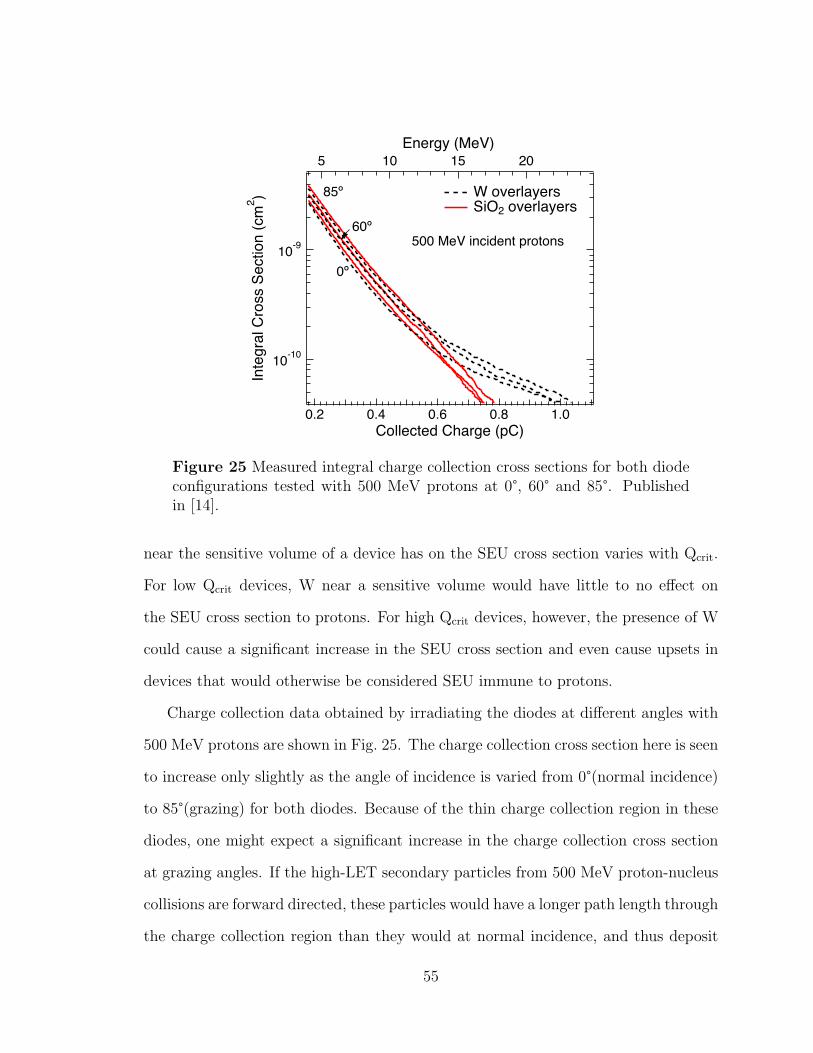
10-10
10-9In
tegr
al C
ross
Sec
tion
(cm
2 )
1.00.80.60.40.2Collected Charge (pC)
2015105Energy (MeV)
0º
85º
60º500 MeV incident protons
W overlayers SiO2 overlayers
Figure 25 Measured integral charge collection cross sections for both diodeconfigurations tested with 500 MeV protons at 0°, 60° and 85°. Publishedin [14].
near the sensitive volume of a device has on the SEU cross section varies with Qcrit.
For low Qcrit devices, W near a sensitive volume would have little to no e↵ect on
the SEU cross section to protons. For high Qcrit devices, however, the presence of W
could cause a significant increase in the SEU cross section and even cause upsets in
devices that would otherwise be considered SEU immune to protons.
Charge collection data obtained by irradiating the diodes at di↵erent angles with
500 MeV protons are shown in Fig. 25. The charge collection cross section here is seen
to increase only slightly as the angle of incidence is varied from 0°(normal incidence)
to 85°(grazing) for both diodes. Because of the thin charge collection region in these
diodes, one might expect a significant increase in the charge collection cross section
at grazing angles. If the high-LET secondary particles from 500 MeV proton-nucleus
collisions are forward directed, these particles would have a longer path length through
the charge collection region than they would at normal incidence, and thus deposit
55
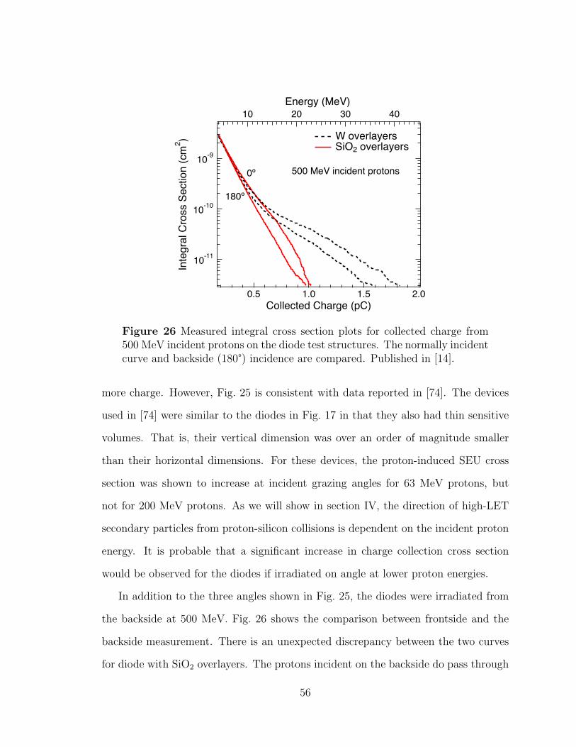
10-11
10-10
10-9
Inte
gral
Cro
ss S
ectio
n (c
m2 )
2.01.51.00.5Collected Charge (pC)
40302010Energy (MeV)
0º
180º
500 MeV incident protons
W overlayers SiO2 overlayers
Figure 26 Measured integral cross section plots for collected charge from500 MeV incident protons on the diode test structures. The normally incidentcurve and backside (180°) incidence are compared. Published in [14].
more charge. However, Fig. 25 is consistent with data reported in [74]. The devices
used in [74] were similar to the diodes in Fig. 17 in that they also had thin sensitive
volumes. That is, their vertical dimension was over an order of magnitude smaller
than their horizontal dimensions. For these devices, the proton-induced SEU cross
section was shown to increase at incident grazing angles for 63 MeV protons, but
not for 200 MeV protons. As we will show in section IV, the direction of high-LET
secondary particles from proton-silicon collisions is dependent on the incident proton
energy. It is probable that a significant increase in charge collection cross section
would be observed for the diodes if irradiated on angle at lower proton energies.
In addition to the three angles shown in Fig. 25, the diodes were irradiated from
the backside at 500 MeV. Fig. 26 shows the comparison between frontside and the
backside measurement. There is an unexpected discrepancy between the two curves
for diode with SiO2 overlayers. The protons incident on the backside do pass through
56
a few millimeters of packaging and substrate materials, however the LET (in Si)
of 500 MeV protons is ⇡ 2 ⇥ 10�3 MeV·cm2/mg, so the protons would only lose a
few MeV of energy by passing through the backside materials. Since protons inci-
dent at both angles would react with silicon nuclei to produce high-LET secondary
particles, one would expect a similar cross section curve. A possible cause of the
discrepancy would be unforeseen materials present near the diode. The secondary
products from proton interactions with these materials would likely be ranged out in
the silicon substrate, and thus be absent in the backside measurement, but would con-
tribute to the charge collection in the normally incident protons. This would account
for the larger cross section curve for the normally incident protons.
Fig. 26 also shows comparable charge collection measurements for the diodes with
W overlayers for both frontside and backside irradiations, even though W was only
present above the sensitive volume. This shows that the proton-induced fission reac-
tion products are relatively isotropic in their direction of emission, as confirmed by
computer simulations in the following section. Simulations also show that proton-
induced spallation fragments tend to be forward directed, and thus aren’t the major
cause of the high charge collection events.
Monte Carlo Simulations
Model Validation
In addition to providing insight into the role of overlayer metallization on charge
deposition in devices exposed to protons, the data from section IV also allow for vali-
dation of SEE modeling tools for proton e↵ects. The well-defined layers and sensitive
volumes of the diodes lend themselves to straightforward modeling. For the computer
simulations performed in this study, the MRED tool developed at Vanderbilt Univer-
57
sity [43] was used. The physics models used for validation against experimental data
in Fig. 27 are given in Table 3.
Simulations of protons normally incident on both diode configurations were run
with the hadronic models listed above for 90, 200, and 500 MeV protons. Fig. 27
shows these simulation results along with the experimental data. The experimental
data are represented by a band due to the uncertainty in the energy calibration of
the measurements. This error was not represented in Figs. 23-26 because each of
those data sets had the same calibration error so the data are still comparable to
one another without taking this calibration uncertainty into consideration. All of
the models except the Bertini Cascade show good agreement for the SiO2 overlayer
diode configurations for 90 and 200 MeV protons, and that the JQMD/PHITS model
significantly overpredicts the data at 500 MeV particularly for the W overlayer con-
figuration. An important observation from Fig. 27 is that the Bertini Cascade shows
almost no di↵erence in its predictions for the two di↵erent diode configurations at
any proton energy. Note that it was the Bertini Cascade model that Howe et al. [5]
used in their study which also showed no di↵erence in calculated proton-induced SEU
cross section when a W overlayer was present. Fig. 27 shows the great importance of
model validation with experimental data.
The reason for the behavior of the Geant4 Bertini Cascade model seen in Fig. 27
was investigated by looking at proton-W secondary particles with MRED. The simu-
lations showed that the Bertini Cascade was predicting high-LET secondary particles
from proton-induced fission for both 200 and 500 MeV protons, however the branch-
ing ratios for the production of these particles were one to two orders of magnitude
lower than the branching ratios calculated with the Geant4 Binary Cascade model.
Note that even though this model includes proton-induced spallation of W, it shows
no predicted di↵erence in the charge collected cross section for the device with W
58
10-12
10-11
10-10
10-9
10-8
Inte
gral
Cro
ss S
ectio
n (c
m2 )
30252015105Energy (MeV)
1.21.00.80.60.40.2Collected Charge (pC)
W overlayer: Experiment Binary Cascade PHITS Bertini G4QMD CEM
SiO2 overlayer:
Experiment Binary Cascade PHITS Bertini G4QMD CEM
90 MeV Protons
10-12
10-11
10-10
10-9
10-8
Inte
gral
Cro
ss S
ectio
n (c
m2 )
5040302010Energy (MeV)
2.01.51.00.5Collected Charge (pC)
W overlayer: Experiment Binary Cascade PHITS Bertini G4QMD CEM
SiO2 overlayer:
Experiment Binary Cascade PHITS Bertini G4QMD CEM
200 MeV Protons
10-12
10-11
10-10
10-9
10-8
Inte
gral
Cro
ss S
ectio
n (c
m2 )
5040302010Energy (MeV)
2.01.51.00.5Collected Charge (pC)
W overlayer: Experiment Binary Cascade PHITS Bertini G4QMD CEM
SiO2 overlayer:
Experiment Binary Cascade PHITS Bertini G4QMD CEM
500 MeV Protons
Figure 27 Comparison of computer simulations done with MRED callingdi↵erent hadronic physics models for 90, 200 and 500 MeV protons normallyincident on both of the diode structures shown in Fig. 17. The shaded bandsrepresenting the experimental data are plotted as such to represent the un-certainty in the energy calibration of the data. The CEM model is seen toprovide the best overall comparison with the experimental data and is thusused for the remainder of the simulations in this paper. Published in [14].
59
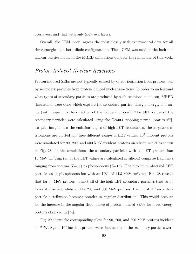
overlayers, and that with only SiO2 overlayers.
Overall, the CEM model agrees the most closely with experimental data for all
three energies and both diode configurations. Thus, CEM was used as the hadronic
nuclear physics model in the MRED simulations done for the remainder of this work.
Proton-Induced Nuclear Reactions
Proton-induced SEEs are not typically caused by direct ionization from protons, but
by secondary particles from proton-induced nuclear reactions. In order to understand
what types of secondary particles are produced by such reactions on silicon, MRED
simulations were done which capture the secondary particle charge, energy, and an-
gle (with respect to the direction of the incident proton). The LET values of the
secondary particles were calculated using the Geant4 stopping power libraries [67].
To gain insight into the emission angles of high-LET secondaries, the angular dis-
tributions are plotted for three di↵erent ranges of LET values. 105 incident protons
were simulated for 90, 200, and 500 MeV incident protons on silicon nuclei as shown
in Fig. 28. In the simulations, the secondary particles with an LET greater than
10 MeV·cm2/mg (all of the LET values are calculated in silicon) comprise fragments
ranging from sodium (Z=11) to phosphorous (Z=15). The maximum observed LET
particle was a phosphorous ion with an LET of 14.3 MeV·cm2/mg. Fig. 28 reveals
that for 90 MeV protons, almost all of the high-LET secondary particles tend to be
forward directed, while for the 200 and 500 MeV protons, the high-LET secondary
particle distribution becomes broader in angular distribution. This would account
for the increase in the angular dependence of proton-induced SEUs for lower energy
protons observed in [74].
Fig. 29 shows the corresponding plots for 90, 200, and 500 MeV protons incident
on 184W. Again, 105 incident protons were simulated and the secondary particles were
60
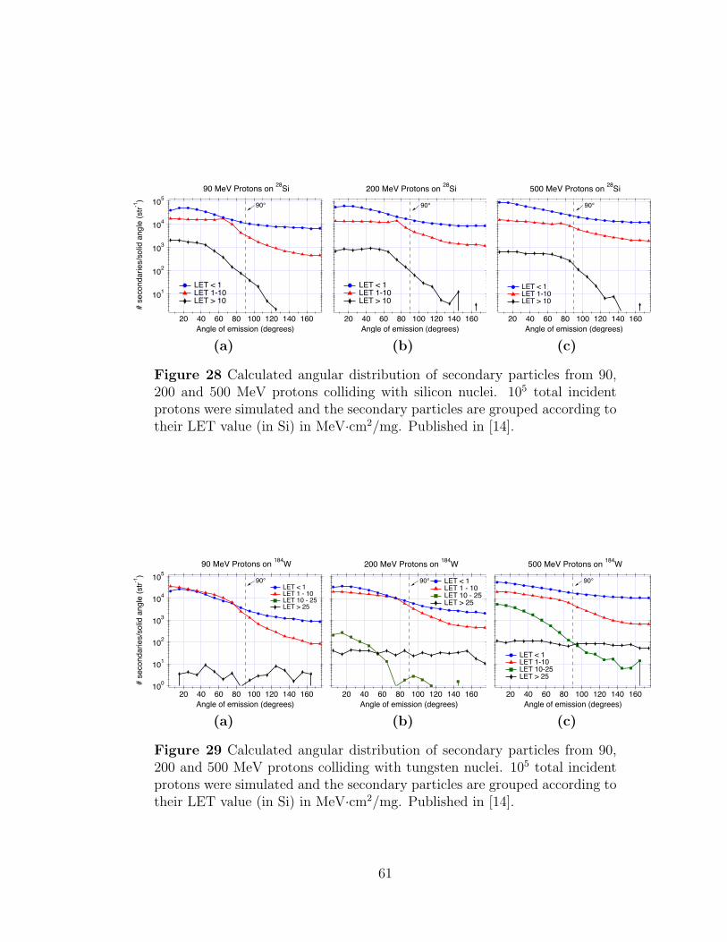
101
102
103
104
105
# s
econ
darie
s/so
lid a
ngle
(str-1
)
16014012010080604020Angle of emission (degrees)
90°
LET < 1 LET 1-10 LET > 10
90 MeV Protons on 28Si
(a)
16014012010080604020Angle of emission (degrees)
90°
LET < 1 LET 1-10 LET > 10
200 MeV Protons on 28Si
(b)
16014012010080604020Angle of emission (degrees)
90°
LET < 1 LET 1-10 LET > 10
500 MeV Protons on 28Si
(c)
Figure 28 Calculated angular distribution of secondary particles from 90,200 and 500 MeV protons colliding with silicon nuclei. 105 total incidentprotons were simulated and the secondary particles are grouped according totheir LET value (in Si) in MeV·cm2/mg. Published in [14].
100
101
102
103
104
105
# s
econ
darie
s/so
lid a
ngle
(str-1
)
16014012010080604020Angle of emission (degrees)
90° LET < 1 LET 1 - 10 LET 10 - 25 LET > 25
90 MeV Protons on 184W
(a)
16014012010080604020Angle of emission (degrees)
90° LET < 1 LET 1 - 10 LET 10 - 25 LET > 25
200 MeV Protons on 184W
(b)
16014012010080604020Angle of emission (degrees)
90°
LET < 1 LET 1-10 LET 10-25 LET > 25
500 MeV Protons on 184W
(c)
Figure 29 Calculated angular distribution of secondary particles from 90,200 and 500 MeV protons colliding with tungsten nuclei. 105 total incidentprotons were simulated and the secondary particles are grouped according totheir LET value (in Si) in MeV·cm2/mg. Published in [14].
61
grouped according to their LET values and plotted versus emission angle. In this case,
the secondaries with an LET greater than 10 MeV·cm2/mg range from sulfur (Z=16)
to rhenium (Z=75). All of the fragments with an LET greater than 25 MeV·cm2/mg
are originate from proton-induced fission. These fission fragments have a maximum
observed LET value of 42 MeV·cm2/mg, and particle species ranging from germanium
(Z=32) to tin (Z=50). The ranges of these fission products are between 4 µm and
22 µm. So sensitive volumes within ⇡20 µm of tungsten in an integrated circuit have
the potential to e↵ected by proton-induced fission products and these products have
the possibility of producing unexpected SEEs in devices [6]. In addition, two fission
fragments from a single proton-W collision, both with a long range, and a high LET,
have the potential to cause proton-induced multiple-bit upsets in devices that have
closely spaced sensitive volumes, although these events would be rare.
A comparison of Figs. 28 and 29 reveals that high-LET secondary particles (LET
> 10 MeV·cm2/mg) have a significantly more isotropic emission for proton-W re-
actions than for proton-Si reactions. In fact, the proton-induced fission fragments
with an LET > 25 MeV·cm2/mg, are seen to be almost completely isotropic in their
emission. This is because proton-induced fission of W occurs in the latter stages of
a nuclear reaction, after the reaction has reached equilibrium and the excited nu-
cleus doesn’t have a memory of the initial direction of the incident particle. For the
proton-spallation reaction (such as those depicted in Fig. 28), many of the high-LET
secondary particles are the residual nucleus after and their emission angle is somewhat
dependent on the direction of the incident proton. Thus, the high-LET secondary
particles from the proton-induced spallation reaction do show a higher probability
of being emitted in the forward direction. This is in agreement with the backside
irradiation measurements shown in Fig. 26.
62
Conclusions
Experimental data presented here show that the presence of high-Z materials, like
tungsten, can significantly increase the charge collection cross section for high in-
cident proton energies, and large charge collection events. This means that high-Z
materials can increase the proton-induced SEU cross section for high-energy protons
and high critical charge devices. The SEU cross section will increase with higher en-
ergy protons for a device with any critical charge, but the e↵ect is more dramatic for
devices with a high critical charge. Monte Carlo simulations show that the high-LET
secondary particles from a proton-W collision originate from proton-induced fission.
These fission fragments are seen to have an LET greater than 25 MeV·cm2/mg, are
emitted isotropically and have a range up to ⇡20 µm.
63
CHAPTER V
MECHANISMS OF NEUTRON-INDUCED
SINGLE EVENT EFFECTS
Introduction
Neutron-induced single event upsets (SEUs) have become a major concern for the
reliability of modern and developing semiconductor technologies [8, 9]. As device
dimensions continue to shrink, the susceptibility to neutron-induced multiple bit up-
sets (MBUs) in static random access memories (SRAMs) is increasing [75,76]. Recent
studies have shown that MBUs must be taken into account for 130 nm and smaller
technology nodes [76]. Although error correcting codes and bit interleaving can e↵ec-
tively reduce the MBU rate, they increase the memory complexity and access time,
and may not be suitable for all memories [29, 47].
Neutrons are not ionizing particles, and thus cannot directly cause SEUs. Neutron-
induced SEUs are caused by secondary particles from nuclear interactions between
energetic neutrons and the materials in and around a device. Modern semiconductor
devices are composed of many materials other than silicon, aluminum, and SiO2. It is
important for current and future technologies to understand how these materials can
a↵ect SEU susceptibility. It has been shown that high-energy protons (>100 MeV)
can trigger fission events in tungsten (W), and that the resulting fission fragments
can have a significantly higher linear energy transfer (LET) and a longer range than
silicon or oxygen recoil atoms (see Chapter IV). It is known that highly energetic
neutrons can also trigger fission events in otherwise stable W nuclei [77], but it has
64
not been assessed how significant these events are for devices in a terrestrial neutron
environment, nor has the impact of these events on MCUs/MBUs been analyzed.
It is ideal to qualify parts in a radiation environment that is as similar to the
natural one as possible. There are a few facilities that provide accelerated neutron
testing with an energy spectrum similar to that of the natural terrestrial environment
[10]. However, due to cost and accessibility, alternative test methods for neutron
vulnerability of electronic devices have been investigated [11,12].
In [12], a comparison was made of the single event upset (SEU) cross sections mea-
sured using a monoenergetic 14 MeV neutron source and the at Los Alamos National
Laboratories’ Weapons Nuclear Research (WNR) facility as shown in Fig. 30. It was
observed that, for multiple SRAMs from various technology nodes, the SEU cross
section measured using 14 MeV neutrons was within a factor of two of that measured
using WNR neutrons. Since the data in [12] were based on only measured cross sec-
tions for devices with feature sizes � 90 nm and no MBU data were available for such
devices, no MBU data were included in [12]. The results presented in this chapter
extends the work of [12] by utilizing the results calibrated Monte Carlo calculations
to obtain the SEU and multiple cell upset (MCU) responses of a prototypical 65 nm
SRAM, and comparing the responses to both 14 MeV and WNR neutron fields.
In this chapter, experimental charge collection data are presented that demon-
strate the e↵ect that high-Z materials near sensitive volumes can have on SEUs for
devices in a terrestrial neutron environment. For each charge collection event the
incident neutron’s time-of-flight (TOF) was measured, thereby showing the e↵ect
that neutron energy has on charge deposition. Through Monte Carlo simulations,
the e↵ect that high-Z materials and neutron energy can have on SEUs and MCUs is
investigated for a representative SRAM structure. Finally, we compare the simulated
SEU and MCU response of this SRAM structure when exposed to the WNR neutron
65
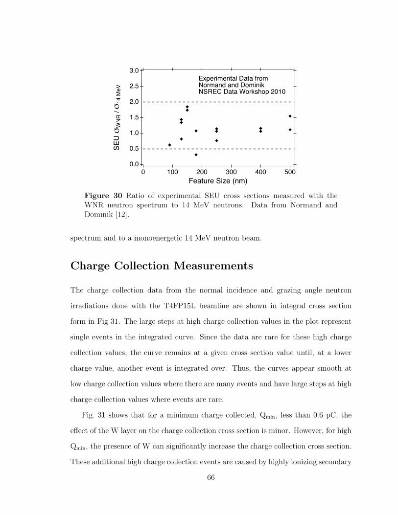
3.0
2.5
2.0
1.5
1.0
0.5
0.0
SEU
mW
NR
/ m
14 M
eV
5004003002001000Feature Size (nm)
Experimental Data from Normand and Dominik NSREC Data Workshop 2010
Figure 30 Ratio of experimental SEU cross sections measured with theWNR neutron spectrum to 14 MeV neutrons. Data from Normand andDominik [12].
spectrum and to a monoenergetic 14 MeV neutron beam.
Charge Collection Measurements
The charge collection data from the normal incidence and grazing angle neutron
irradiations done with the T4FP15L beamline are shown in integral cross section
form in Fig 31. The large steps at high charge collection values in the plot represent
single events in the integrated curve. Since the data are rare for these high charge
collection values, the curve remains at a given cross section value until, at a lower
charge value, another event is integrated over. Thus, the curves appear smooth at
low charge collection values where there are many events and have large steps at high
charge collection values where events are rare.
Fig. 31 shows that for a minimum charge collected, Qmin, less than 0.6 pC, the
e↵ect of the W layer on the charge collection cross section is minor. However, for high
Qmin, the presence of W can significantly increase the charge collection cross section.
These additional high charge collection events are caused by highly ionizing secondary
66
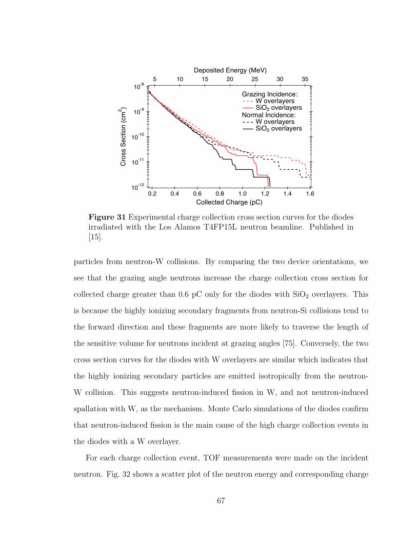
10-12
10-11
10-10
10-9
10-8
Cros
s Se
ctio
n (c
m2 )
3530252015105 Deposited Energy (MeV)
1.61.41.21.00.80.60.40.2Collected Charge (pC)
Grazing Incidence: W overlayers SiO2 overlayers
Normal Incidence: W overlayers SiO2 overlayers
Figure 31 Experimental charge collection cross section curves for the diodesirradiated with the Los Alamos T4FP15L neutron beamline. Published in[15].
particles from neutron-W collisions. By comparing the two device orientations, we
see that the grazing angle neutrons increase the charge collection cross section for
collected charge greater than 0.6 pC only for the diodes with SiO2 overlayers. This
is because the highly ionizing secondary fragments from neutron-Si collisions tend to
the forward direction and these fragments are more likely to traverse the length of
the sensitive volume for neutrons incident at grazing angles [75]. Conversely, the two
cross section curves for the diodes with W overlayers are similar which indicates that
the highly ionizing secondary particles are emitted isotropically from the neutron-
W collision. This suggests neutron-induced fission in W, and not neutron-induced
spallation with W, as the mechanism. Monte Carlo simulations of the diodes confirm
that neutron-induced fission is the main cause of the high charge collection events in
the diodes with a W overlayer.
For each charge collection event, TOF measurements were made on the incident
neutron. Fig. 32 shows a scatter plot of the neutron energy and corresponding charge
67
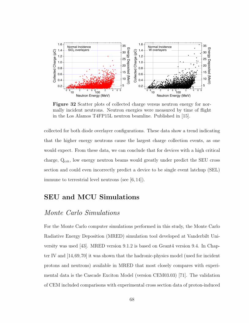
35
30
25
20
15
10
5
Energy Deposited (MeV)
6 810
2 4 6 8100
2 4 6 8
Neutron Energy (MeV)
1.6
1.4
1.2
1.0
0.8
0.6
0.4
0.2
Colle
cted
Cha
rge
(pC)
Normal Incidence SiO2 overlayers
35
30
25
20
15
10
5
Energy Deposited (M
eV)
6 810
2 4 6 8100
2 4 6 8
Neutron Energy (MeV)
1.6
1.4
1.2
1.0
0.8
0.6
0.4
0.2
Col
lect
ed C
harg
e (p
C) Normal Incidence
W overlayers
Figure 32 Scatter plots of collected charge versus neutron energy for nor-mally incident neutrons. Neutron energies were measured by time of flightin the Los Alamos T4FP15L neutron beamline. Published in [15].
collected for both diode overlayer configurations. These data show a trend indicating
that the higher energy neutrons cause the largest charge collection events, as one
would expect. From these data, we can conclude that for devices with a high critical
charge, Qcrit, low energy neutron beams would greatly under predict the SEU cross
section and could even incorrectly predict a device to be single event latchup (SEL)
immune to terrestrial level neutrons (see [6, 14]).
SEU and MCU Simulations
Monte Carlo Simulations
For the Monte Carlo computer simulations performed in this study, the Monte Carlo
Radiative Energy Deposition (MRED) simulation tool developed at Vanderbilt Uni-
versity was used [43]. MRED version 9.1.2 is based on Geant4 version 9.4. In Chap-
ter IV and [14,69,70] it was shown that the hadronic-physics model (used for incident
protons and neutrons) available in MRED that most closely compares with experi-
mental data is the Cascade Exciton Model (version CEM03.03) [71]. The validation
of CEM included comparisons with experimental cross section data of proton-induced
68
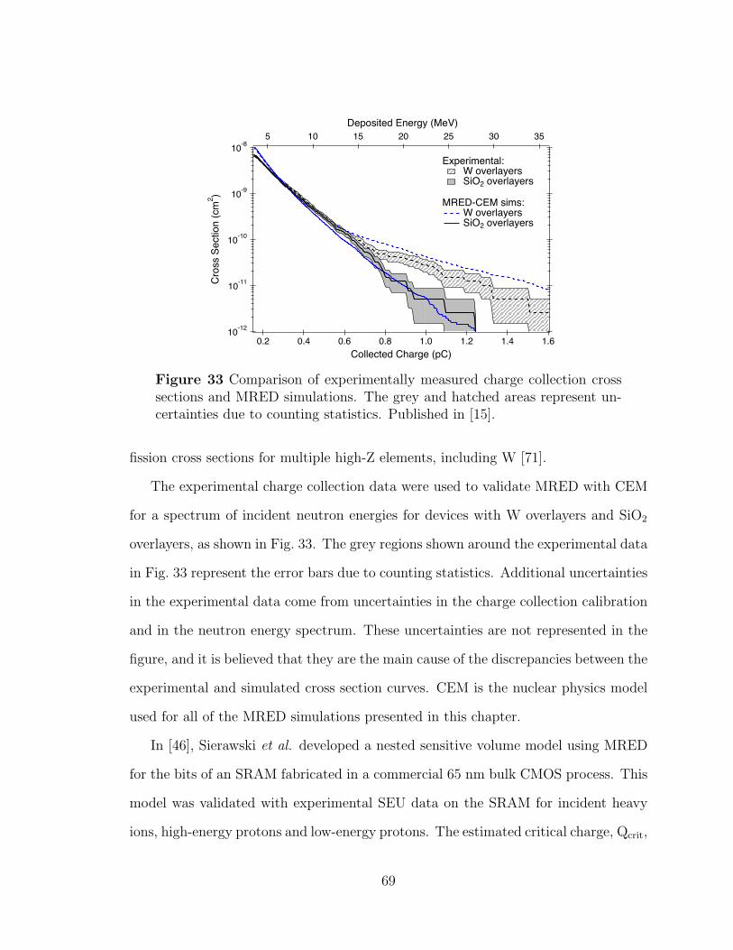
10-12
10-11
10-10
10-9
10-8
Cros
s Se
ctio
n (c
m2 )
3530252015105 Deposited Energy (MeV)
1.61.41.21.00.80.60.40.2Collected Charge (pC)
Experimental: W overlayers SiO2 overlayers
MRED-CEM sims:
W overlayers SiO2 overlayers
Figure 33 Comparison of experimentally measured charge collection crosssections and MRED simulations. The grey and hatched areas represent un-certainties due to counting statistics. Published in [15].
fission cross sections for multiple high-Z elements, including W [71].
The experimental charge collection data were used to validate MRED with CEM
for a spectrum of incident neutron energies for devices with W overlayers and SiO2
overlayers, as shown in Fig. 33. The grey regions shown around the experimental data
in Fig. 33 represent the error bars due to counting statistics. Additional uncertainties
in the experimental data come from uncertainties in the charge collection calibration
and in the neutron energy spectrum. These uncertainties are not represented in the
figure, and it is believed that they are the main cause of the discrepancies between the
experimental and simulated cross section curves. CEM is the nuclear physics model
used for all of the MRED simulations presented in this chapter.
In [46], Sierawski et al. developed a nested sensitive volume model using MRED
for the bits of an SRAM fabricated in a commercial 65 nm bulk CMOS process. This
model was validated with experimental SEU data on the SRAM for incident heavy
ions, high-energy protons and low-energy protons. The estimated critical charge, Qcrit,
69
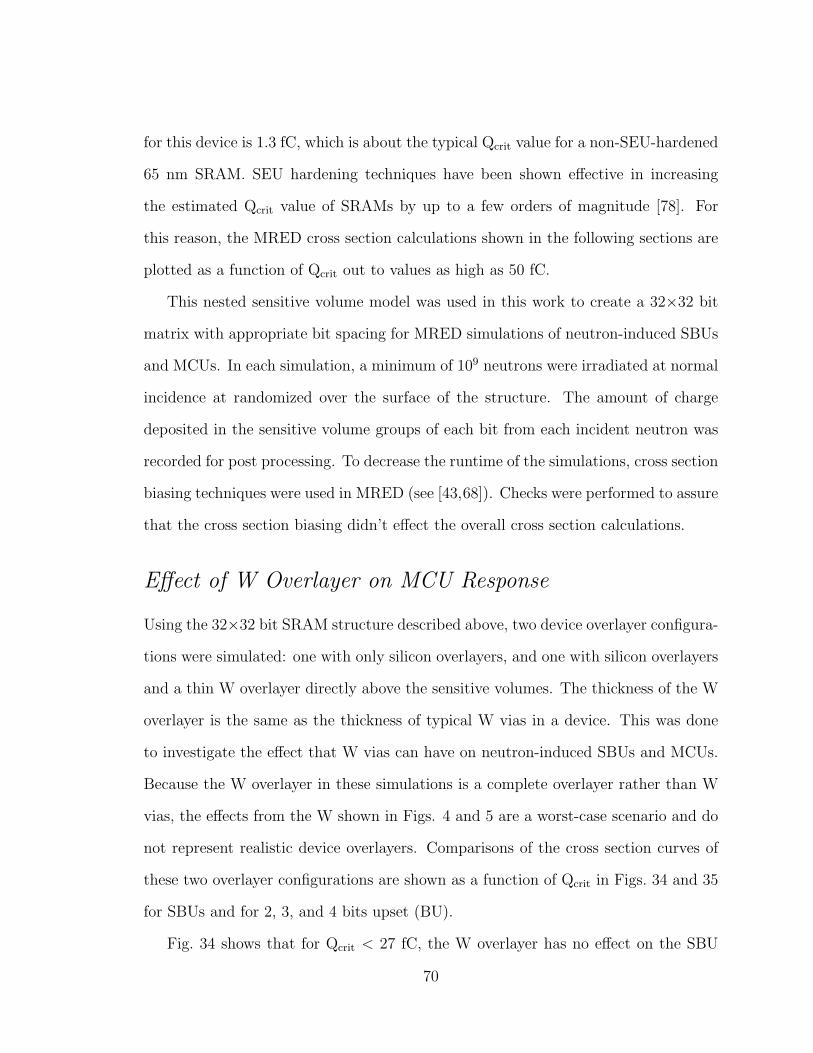
for this device is 1.3 fC, which is about the typical Qcrit value for a non-SEU-hardened
65 nm SRAM. SEU hardening techniques have been shown e↵ective in increasing
the estimated Qcrit value of SRAMs by up to a few orders of magnitude [78]. For
this reason, the MRED cross section calculations shown in the following sections are
plotted as a function of Qcrit out to values as high as 50 fC.
This nested sensitive volume model was used in this work to create a 32⇥32 bit
matrix with appropriate bit spacing for MRED simulations of neutron-induced SBUs
and MCUs. In each simulation, a minimum of 109 neutrons were irradiated at normal
incidence at randomized over the surface of the structure. The amount of charge
deposited in the sensitive volume groups of each bit from each incident neutron was
recorded for post processing. To decrease the runtime of the simulations, cross section
biasing techniques were used in MRED (see [43,68]). Checks were performed to assure
that the cross section biasing didn’t e↵ect the overall cross section calculations.
E↵ect of W Overlayer on MCU Response
Using the 32⇥32 bit SRAM structure described above, two device overlayer configura-
tions were simulated: one with only silicon overlayers, and one with silicon overlayers
and a thin W overlayer directly above the sensitive volumes. The thickness of the W
overlayer is the same as the thickness of typical W vias in a device. This was done
to investigate the e↵ect that W vias can have on neutron-induced SBUs and MCUs.
Because the W overlayer in these simulations is a complete overlayer rather than W
vias, the e↵ects from the W shown in Figs. 4 and 5 are a worst-case scenario and do
not represent realistic device overlayers. Comparisons of the cross section curves of
these two overlayer configurations are shown as a function of Qcrit in Figs. 34 and 35
for SBUs and for 2, 3, and 4 bits upset (BU).
Fig. 34 shows that for Qcrit < 27 fC, the W overlayer has no e↵ect on the SBU
70
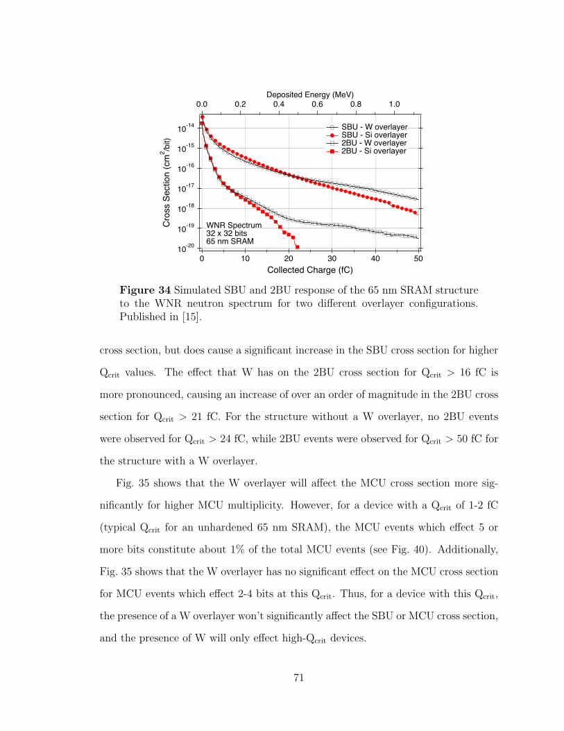
10-20
10-19
10-18
10-17
10-16
10-15
10-14
Cro
ss S
ectio
n (c
m2 /b
it)
50403020100Collected Charge (fC)
1.00.80.60.40.20.0Deposited Energy (MeV)
SBU - W overlayer SBU - Si overlayer 2BU - W overlayer 2BU - Si overlayer
WNR Spectrum32 x 32 bits65 nm SRAM
Figure 34 Simulated SBU and 2BU response of the 65 nm SRAM structureto the WNR neutron spectrum for two di↵erent overlayer configurations.Published in [15].
cross section, but does cause a significant increase in the SBU cross section for higher
Qcrit values. The e↵ect that W has on the 2BU cross section for Qcrit > 16 fC is
more pronounced, causing an increase of over an order of magnitude in the 2BU cross
section for Qcrit > 21 fC. For the structure without a W overlayer, no 2BU events
were observed for Qcrit > 24 fC, while 2BU events were observed for Qcrit > 50 fC for
the structure with a W overlayer.
Fig. 35 shows that the W overlayer will a↵ect the MCU cross section more sig-
nificantly for higher MCU multiplicity. However, for a device with a Qcrit of 1-2 fC
(typical Qcrit for an unhardened 65 nm SRAM), the MCU events which e↵ect 5 or
more bits constitute about 1% of the total MCU events (see Fig. 40). Additionally,
Fig. 35 shows that the W overlayer has no significant e↵ect on the MCU cross section
for MCU events which e↵ect 2-4 bits at this Qcrit. Thus, for a device with this Qcrit,
the presence of a W overlayer won’t significantly a↵ect the SBU or MCU cross section,
and the presence of W will only e↵ect high-Qcrit devices.
71
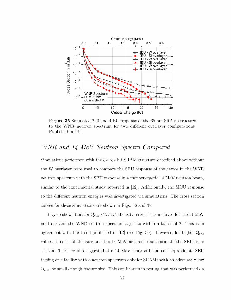
10-20
10-19
10-18
10-17
10-16
10-15
10-14
Cro
ss S
ectio
n (c
m2 /b
it)
302520151050Critical Charge (fC)
0.60.50.40.30.20.10.0Critical Energy (MeV)
2BU - W overlayer 2BU - Si overlayer 3BU - W overlayer 3BU - Si overlayer 4BU - W overlayer 4BU - Si overlayer
WNR Spectrum32 x 32 bits65 nm SRAM
Figure 35 Simulated 2, 3 and 4 BU response of the 65 nm SRAM structureto the WNR neutron spectrum for two di↵erent overlayer configurations.Published in [15].
WNR and 14 MeV Neutron Spectra Compared
Simulations performed with the 32⇥32 bit SRAM structure described above without
the W overlayer were used to compare the SBU response of the device in the WNR
neutron spectrum with the SBU response in a monoenergetic 14 MeV neutron beam,
similar to the experimental study reported in [12]. Additionally, the MCU response
to the di↵erent neutron energies was investigated via simulations. The cross section
curves for these simulations are shown in Figs. 36 and 37.
Fig. 36 shows that for Qcrit < 27 fC, the SBU cross section curves for the 14 MeV
neutrons and the WNR neutron spectrum agree to within a factor of 2. This is in
agreement with the trend published in [12] (see Fig. 30). However, for higher Qcrit
values, this is not the case and the 14 MeV neutrons underestimate the SBU cross
section. These results suggest that a 14 MeV neutron beam can approximate SEU
testing at a facility with a neutron spectrum only for SRAMs with an adequately low
Qcrit, or small enough feature size. This can be seen in testing that was performed on
72
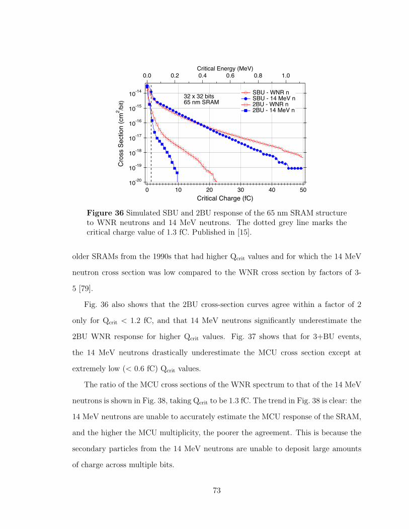
10-20
10-19
10-18
10-17
10-16
10-15
10-14
Cro
ss S
ectio
n (c
m2 /b
it)
50403020100Critical Charge (fC)
1.00.80.60.40.20.0Critical Energy (MeV)
SBU - WNR n SBU - 14 MeV n 2BU - WNR n 2BU - 14 MeV n
32 x 32 bits65 nm SRAM
Figure 36 Simulated SBU and 2BU response of the 65 nm SRAM structureto WNR neutrons and 14 MeV neutrons. The dotted grey line marks thecritical charge value of 1.3 fC. Published in [15].
older SRAMs from the 1990s that had higher Qcrit values and for which the 14 MeV
neutron cross section was low compared to the WNR cross section by factors of 3-
5 [79].
Fig. 36 also shows that the 2BU cross-section curves agree within a factor of 2
only for Qcrit < 1.2 fC, and that 14 MeV neutrons significantly underestimate the
2BU WNR response for higher Qcrit values. Fig. 37 shows that for 3+BU events,
the 14 MeV neutrons drastically underestimate the MCU cross section except at
extremely low (< 0.6 fC) Qcrit values.
The ratio of the MCU cross sections of the WNR spectrum to that of the 14 MeV
neutrons is shown in Fig. 38, taking Qcrit to be 1.3 fC. The trend in Fig. 38 is clear: the
14 MeV neutrons are unable to accurately estimate the MCU response of the SRAM,
and the higher the MCU multiplicity, the poorer the agreement. This is because the
secondary particles from the 14 MeV neutrons are unable to deposit large amounts
of charge across multiple bits.
73
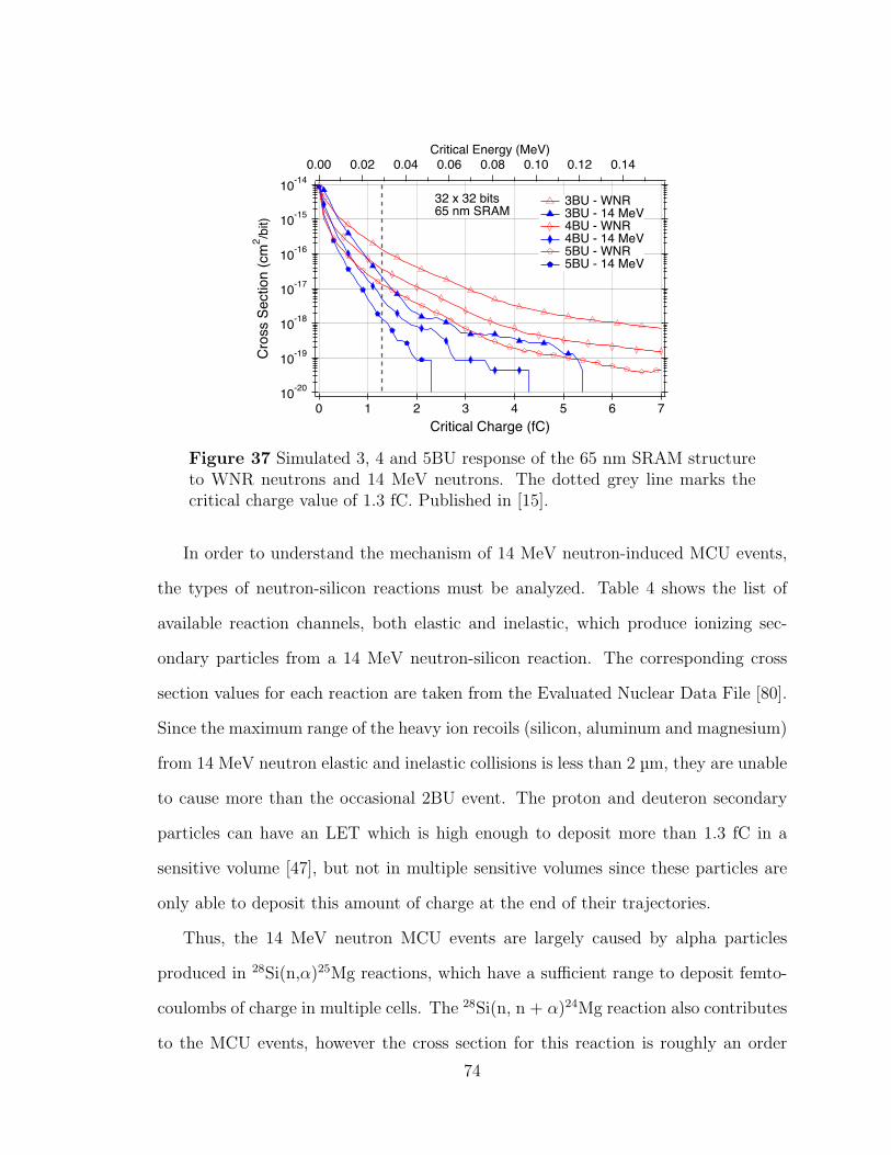
10-20
10-19
10-18
10-17
10-16
10-15
10-14
Cro
ss S
ectio
n (c
m2 /b
it)
76543210Critical Charge (fC)
0.140.120.100.080.060.040.020.00Critical Energy (MeV)
3BU - WNR 3BU - 14 MeV 4BU - WNR 4BU - 14 MeV 5BU - WNR 5BU - 14 MeV
32 x 32 bits65 nm SRAM
Figure 37 Simulated 3, 4 and 5BU response of the 65 nm SRAM structureto WNR neutrons and 14 MeV neutrons. The dotted grey line marks thecritical charge value of 1.3 fC. Published in [15].
In order to understand the mechanism of 14 MeV neutron-induced MCU events,
the types of neutron-silicon reactions must be analyzed. Table 4 shows the list of
available reaction channels, both elastic and inelastic, which produce ionizing sec-
ondary particles from a 14 MeV neutron-silicon reaction. The corresponding cross
section values for each reaction are taken from the Evaluated Nuclear Data File [80].
Since the maximum range of the heavy ion recoils (silicon, aluminum and magnesium)
from 14 MeV neutron elastic and inelastic collisions is less than 2 µm, they are unable
to cause more than the occasional 2BU event. The proton and deuteron secondary
particles can have an LET which is high enough to deposit more than 1.3 fC in a
sensitive volume [47], but not in multiple sensitive volumes since these particles are
only able to deposit this amount of charge at the end of their trajectories.
Thus, the 14 MeV neutron MCU events are largely caused by alpha particles
produced in 28Si(n,↵)25Mg reactions, which have a su�cient range to deposit femto-
coulombs of charge in multiple cells. The 28Si(n, n + ↵)24Mg reaction also contributes
to the MCU events, however the cross section for this reaction is roughly an order
74
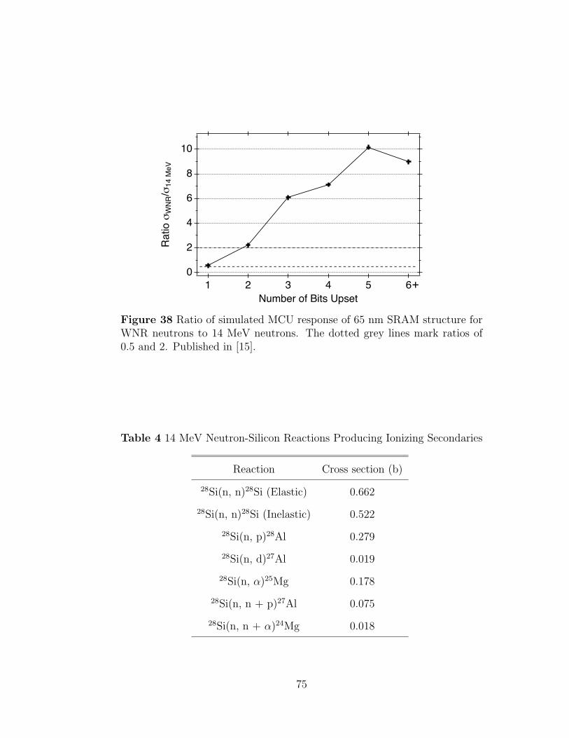
10
8
6
4
2
0
Rat
io �
WN
R/�
14 M
eV
654321Number of Bits Upset
+
Figure 38 Ratio of simulated MCU response of 65 nm SRAM structure forWNR neutrons to 14 MeV neutrons. The dotted grey lines mark ratios of0.5 and 2. Published in [15].
Table 4 14 MeV Neutron-Silicon Reactions Producing Ionizing Secondaries
Reaction Cross section (b)
28Si(n, n)28Si (Elastic) 0.662
28Si(n, n)28Si (Inelastic) 0.522
28Si(n, p)28Al 0.279
28Si(n, d)27Al 0.019
28Si(n, ↵)25Mg 0.178
28Si(n, n + p)27Al 0.075
28Si(n, n + ↵)24Mg 0.018
75
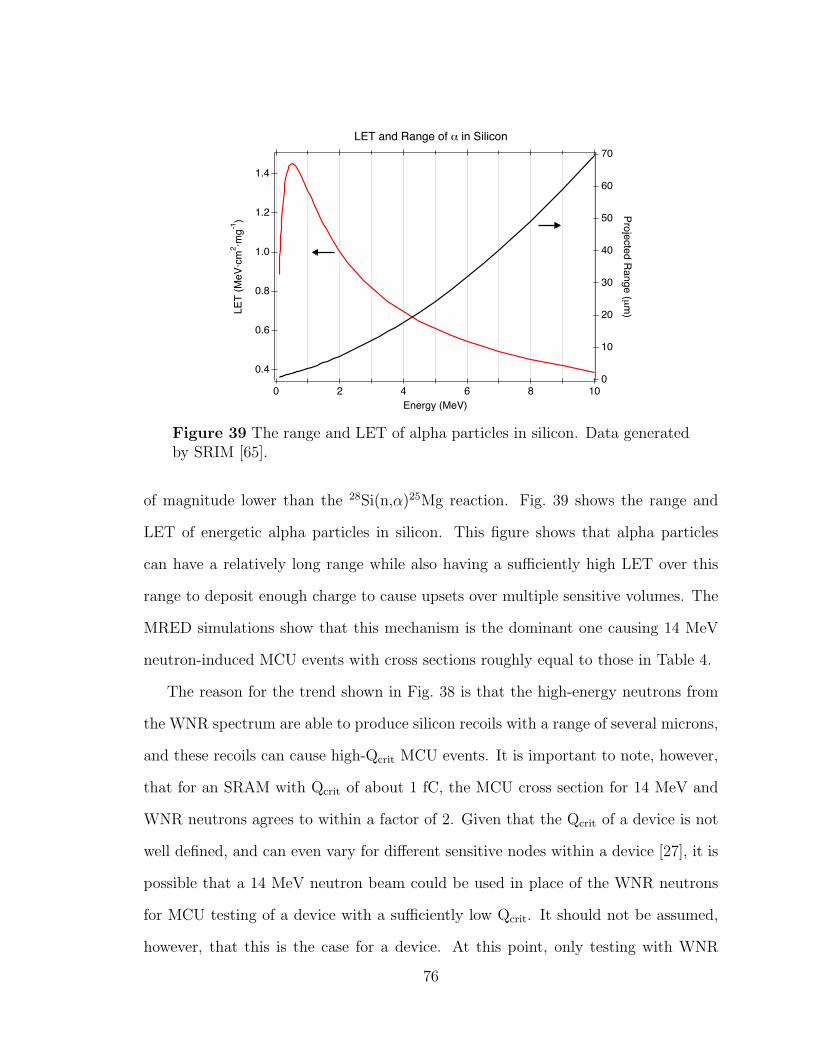
1.4
1.2
1.0
0.8
0.6
0.4
LET
(MeV
·cm
2 ·mg-1
)
1086420Energy (MeV)
70
60
50
40
30
20
10
0
Projected Range (µm
)
LET and Range of _ in Silicon
Figure 39 The range and LET of alpha particles in silicon. Data generatedby SRIM [65].
of magnitude lower than the 28Si(n,↵)25Mg reaction. Fig. 39 shows the range and
LET of energetic alpha particles in silicon. This figure shows that alpha particles
can have a relatively long range while also having a su�ciently high LET over this
range to deposit enough charge to cause upsets over multiple sensitive volumes. The
MRED simulations show that this mechanism is the dominant one causing 14 MeV
neutron-induced MCU events with cross sections roughly equal to those in Table 4.
The reason for the trend shown in Fig. 38 is that the high-energy neutrons from
the WNR spectrum are able to produce silicon recoils with a range of several microns,
and these recoils can cause high-Qcrit MCU events. It is important to note, however,
that for an SRAM with Qcrit of about 1 fC, the MCU cross section for 14 MeV and
WNR neutrons agrees to within a factor of 2. Given that the Qcrit of a device is not
well defined, and can even vary for di↵erent sensitive nodes within a device [27], it is
possible that a 14 MeV neutron beam could be used in place of the WNR neutrons
for MCU testing of a device with a su�ciently low Qcrit. It should not be assumed,
however, that this is the case for a device. At this point, only testing with WNR
76
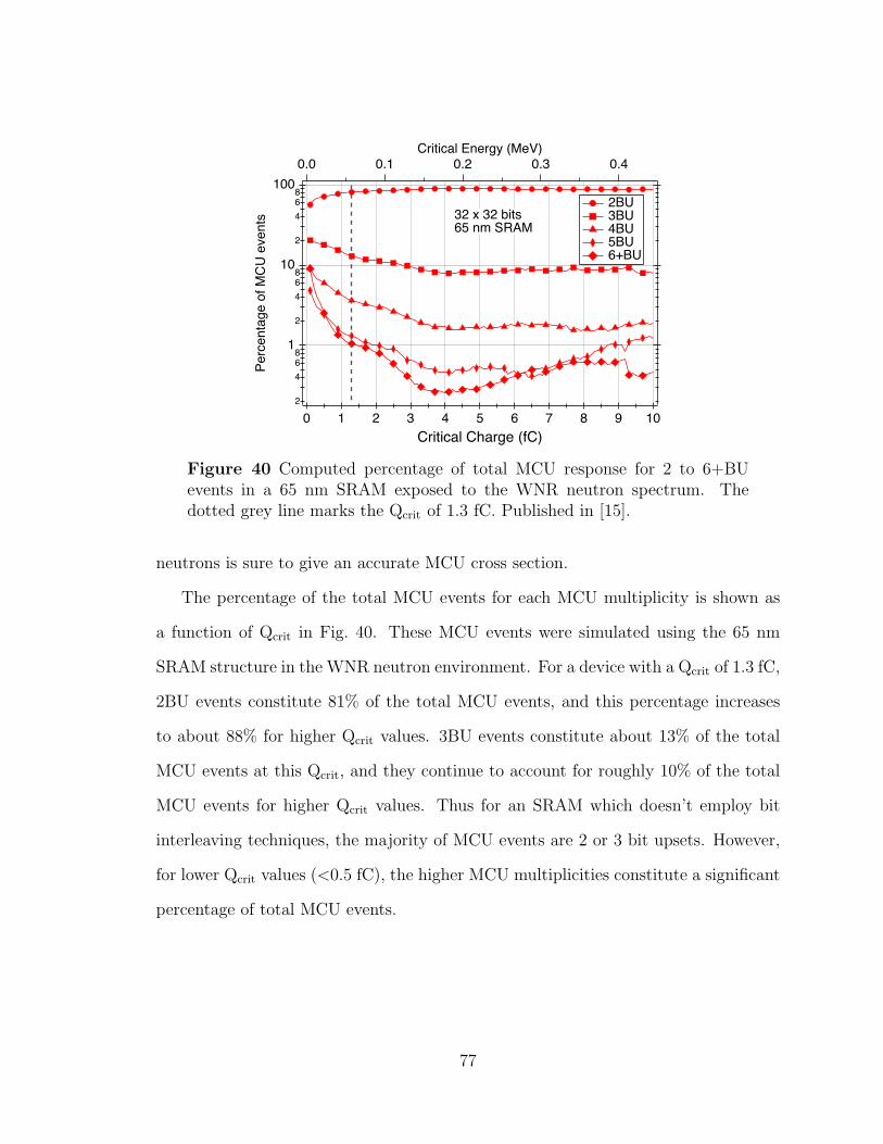
2
468
1
2
468
10
2
468
100
Perc
enta
ge o
f MC
U e
vent
s
109876543210Critical Charge (fC)
0.40.30.20.10.0Critical Energy (MeV)
2BU 3BU 4BU 5BU 6+BU
32 x 32 bits65 nm SRAM
Figure 40 Computed percentage of total MCU response for 2 to 6+BUevents in a 65 nm SRAM exposed to the WNR neutron spectrum. Thedotted grey line marks the Qcrit of 1.3 fC. Published in [15].
neutrons is sure to give an accurate MCU cross section.
The percentage of the total MCU events for each MCU multiplicity is shown as
a function of Qcrit in Fig. 40. These MCU events were simulated using the 65 nm
SRAM structure in the WNR neutron environment. For a device with a Qcrit of 1.3 fC,
2BU events constitute 81% of the total MCU events, and this percentage increases
to about 88% for higher Qcrit values. 3BU events constitute about 13% of the total
MCU events at this Qcrit, and they continue to account for roughly 10% of the total
MCU events for higher Qcrit values. Thus for an SRAM which doesn’t employ bit
interleaving techniques, the majority of MCU events are 2 or 3 bit upsets. However,
for lower Qcrit values (<0.5 fC), the higher MCU multiplicities constitute a significant
percentage of total MCU events.
77
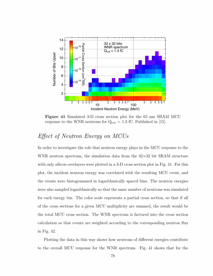
2 3 4 5 6 710
2 3 4 5 6 7100
2 3 4 5 6 7
Incident Neutron Energy (MeV)
14
12
10
8
6
4
2
Num
ber o
f Bits
Ups
et
10-18
32 x 32 bitsWNR spectrumQcrit = 1.3 fC
10-1810-19
10-20
10-21-19
-18
-17
-16
Partial Cross Section (cm
2/bit)
10-16
10-17
10-18
10-19
Figure 41 Simulated 3-D cross section plot for the 65 nm SRAM MCUresponse to the WNR neutrons for Qcrit = 1.3 fC. Published in [15].
E↵ect of Neutron Energy on MCUs
In order to investigate the role that neutron energy plays in the MCU response to the
WNR neutron spectrum, the simulation data from the 32⇥32 bit SRAM structure
with only silicon overlayers were plotted in a 3-D cross section plot in Fig. 41. For this
plot, the incident neutron energy was correlated with the resulting MCU event, and
the events were histogrammed in logarithmically spaced bins. The neutron energies
were also sampled logarithmically so that the same number of neutrons was simulated
for each energy bin. The color scale represents a partial cross section, so that if all
of the cross sections for a given MCU multiplicity are summed, the result would be
the total MCU cross section. The WNR spectrum is factored into the cross section
calculation so that events are weighted according to the corresponding neutron flux
in Fig. 42.
Plotting the data in this way shows how neutrons of di↵erent energies contribute
to the overall MCU response for the WNR spectrum. Fig. 41 shows that for the
78
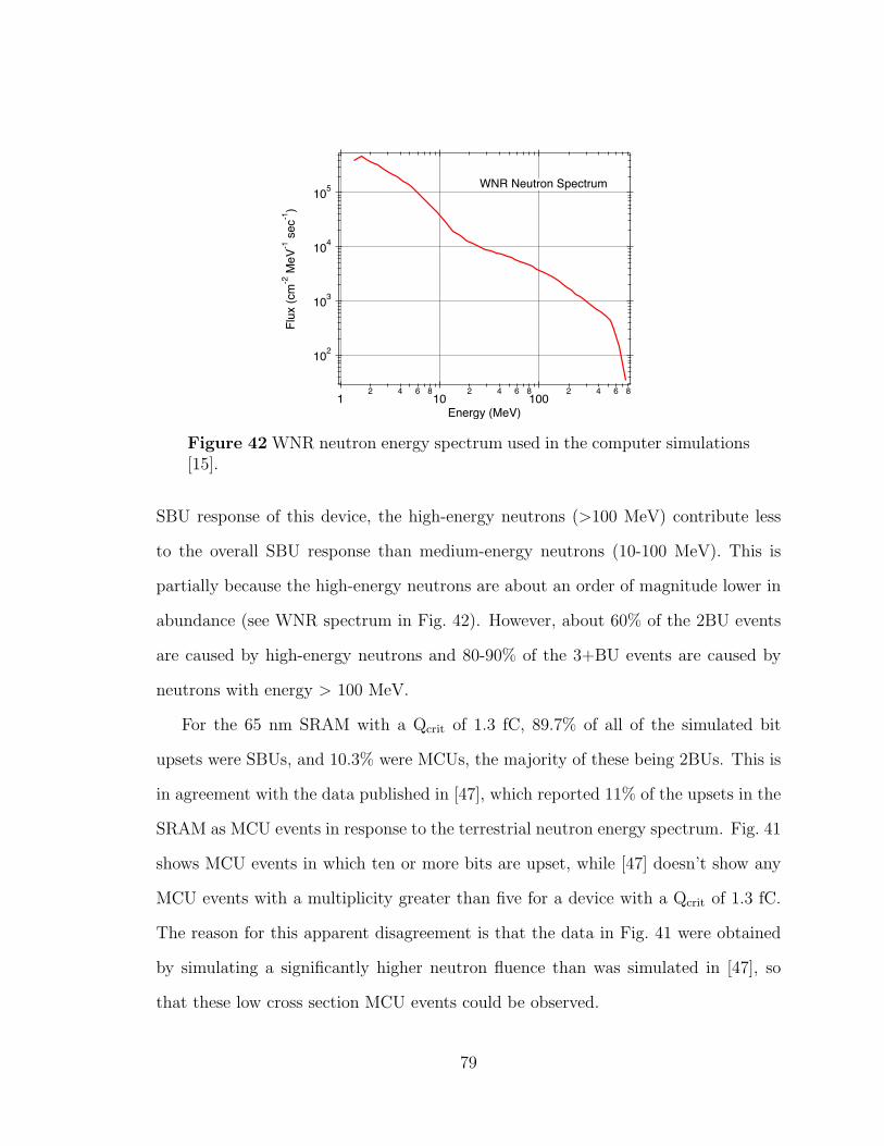
102
103
104
105
Flux
(cm
-2 M
eV-1
sec
-1)
12 4 6 8
102 4 6 8
1002 4 6 8
Energy (MeV)
WNR Neutron Spectrum
Figure 42 WNR neutron energy spectrum used in the computer simulations[15].
SBU response of this device, the high-energy neutrons (>100 MeV) contribute less
to the overall SBU response than medium-energy neutrons (10-100 MeV). This is
partially because the high-energy neutrons are about an order of magnitude lower in
abundance (see WNR spectrum in Fig. 42). However, about 60% of the 2BU events
are caused by high-energy neutrons and 80-90% of the 3+BU events are caused by
neutrons with energy > 100 MeV.
For the 65 nm SRAM with a Qcrit of 1.3 fC, 89.7% of all of the simulated bit
upsets were SBUs, and 10.3% were MCUs, the majority of these being 2BUs. This is
in agreement with the data published in [47], which reported 11% of the upsets in the
SRAM as MCU events in response to the terrestrial neutron energy spectrum. Fig. 41
shows MCU events in which ten or more bits are upset, while [47] doesn’t show any
MCU events with a multiplicity greater than five for a device with a Qcrit of 1.3 fC.
The reason for this apparent disagreement is that the data in Fig. 41 were obtained
by simulating a significantly higher neutron fluence than was simulated in [47], so
that these low cross section MCU events could be observed.
79
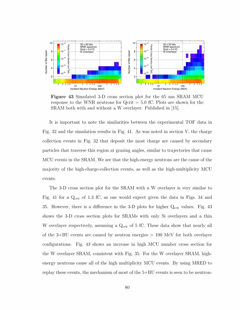
2 3 4 5 610
2 3 4 5 6100
2 3 4 5 6
Incident Neutron Energy (MeV)
10
8
6
4
2
Num
ber o
f Bits
Ups
et32 x 32 bitsWNR spectrumQcrit = 5.0 fCSi Overlayer
-20
-19
-18
-17
-16 Partial Cross Section (cm2/bit)
10-16
10-17
10-18
10-20
10-19
2 3 4 5 610
2 3 4 5 6100
2 3 4 5 6
Incident Neutron Energy (MeV)
10
8
6
4
2
Num
ber o
f Bits
Ups
et
32 x 32 bitsWNR spectrumQcrit = 5.0 fCW Overlayer
-20
-19
-18
-17
-16 Partial Cross Section (cm2/bit)
10-16
10-17
10-18
10-20
10-19
Figure 43 Simulated 3-D cross section plot for the 65 nm SRAM MCUresponse to the WNR neutrons for Qcrit = 5.0 fC. Plots are shown for theSRAM both with and without a W overlayer. Published in [15].
It is important to note the similarities between the experimental TOF data in
Fig. 32 and the simulation results in Fig. 41. As was noted in section V, the charge
collection events in Fig. 32 that deposit the most charge are caused by secondary
particles that traverse this region at grazing angles, similar to trajectories that cause
MCU events in the SRAM. We see that the high-energy neutrons are the cause of the
majority of the high-charge-collection events, as well as the high-multiplicity MCU
events.
The 3-D cross section plot for the SRAM with a W overlayer is very similar to
Fig. 41 for a Qcrit of 1.3 fC, as one would expect given the data in Figs. 34 and
35. However, there is a di↵erence in the 3-D plots for higher Qcrit values. Fig. 43
shows the 3-D cross section plots for SRAMs with only Si overlayers and a thin
W overlayer respectively, assuming a Qcrit of 5 fC. These data show that nearly all
of the 3+BU events are caused by neutron energies > 100 MeV for both overlayer
configurations. Fig. 43 shows an increase in high MCU number cross section for
the W overlayer SRAM, consistent with Fig. 35. For the W overlayer SRAM, high-
energy neutrons cause all of the high multiplicity MCU events. By using MRED to
replay these events, the mechanism of most of the 5+BU events is seen to be neutron-
80
induced fission fragments from a neutron-W collision. One of the energetic and highly
ionizing fragments is emitted at a near 90 angle and travels down a column of cells in
the SRAM, causing the MCU event. Since the neutron-induced fission cross section
is negligible for neutron energies less than 100 MeV, only high-energy neutrons are
able to produce these events.
Conclusions
Experimental data and simulations of 65 nm SRAMs presented here show that the
presence of high-Z materials, like tungsten, can only increase the SEU cross section for
high Qcrit (> 27 fC) devices and can only significantly increase the MCU cross section
for devices with a Qcrit > 16 fC when exposed to the terrestrial neutron environment.
This is due to the presence of high-energy (>100 MeV) neutrons. Simulations with
a solid W overlayer show that for an unhardened devices with a Qcrit of 1-2 fC, the
presence of W does not significantly e↵ect the SEU or MCU cross section.
Simulations show that for 65 nm SRAMs with a Qcrit < 27 fC, a monoenergetic
14 MeV neutron beam can be used to estimate the SEU response to the terrestrial
neutron environment within a factor of two, in agreement with [12]. However, a mo-
noenergetic 14 MeV neutron beam is inadequate to estimate the 2BU response to the
terrestrial neutron environment to within a factor of two, except for devices with a
very low Qcrit (< 1.2 fC). 14 MeV neutrons are not able to adequately simulate the
MCU response of devices in the terrestrial neutron environment for 3+BU events (for
the device simulated here, these events have a cross-section lower than 10-16cm2/bit
i.e. a soft error rate lower than 1.5 FIT/Mb). The experimental data and simula-
tions presented here demonstrate that 14 MeV neutrons produce far fewer high-LET
secondary particles than terrestrial neutrons. Thus, in the context of [12], MCUs are
similar to SEL in that 14 MeV neutrons should not be used as a substitute for the
81
response to a spallation neutron source; only high-energy particle beams may be used
to obtain accurate SEL and MCU responses.
While the 65 nm SRAM structure simulated in this work shows an MCU percent-
age of 10.3%, this is not representative of all 65 nm SRAMs. Previous works have
shown that the MCU percentage of 65 nm SRAMs can vary greatly and can be as
high as 50% or more [81]. Based on the good agreement between simulations and
measurements of the SRAM presented in this work and in [47], we have confidence
that the simulation can be successfully extended to other SRAMs in which the MCU
fraction is much higher.
82
CHAPTER VI
CONCLUSIONS
The research presented here gives new insights into the mechanisms of proton-
and neutron-induced single event upsets (SEUs) relevant to modern-day devices. It is
shown via experimental charge collection measurement and Monte Carlo simulations
that the presence of tungsten (W) in modern day devices can have an impact on both
proton- and neutron-induced SEUs. The mechanism for this is shown to be high-
energy proton- and neutron-induced fission in the W nuclei. These induced fission
events are seen to produce secondary particles with both a high linear energy transfer
(LET) value and a high range and can cause an increase in both the SEU and MCU
cross section of a device, depending on the critical charge, Qcrit.
The results of experimental time of flight measurements coupled with charge col-
lection measurements and Monte Carlo simulations presented here demonstrate the
e↵ect that neutron energy can have on neutron-induced SEUs and MCUs. It is shown
that high-energy neutrons are able to produce higher-LET secondary particles with
a longer range compared to 14 MeV neutrons. However, it is shown the that 14 MeV
neutrons are able to cause the same SEU and MCU cross section in an SRAM de-
vice with a su�ciently low Qcrit. The mechanism for the 14 MeV neutron-induced
MCU events is seen to be secondary alpha particles emitted from the 28Si(n,↵)25Mg
reaction.
The e↵ect of proton and neutron radiation on semiconducting devices will con-
tinue to be an important issue in the developing of new technologies. The research
presented here provides a deeper understanding of the mechanisms behind proton-
83
and neutron-induced radiation e↵ects. As semiconducting devices continue to shrink
in size, these results will provide insight which will aid in the testing of devices and
the understanding of future observations of radiation e↵ects.
84
APPENDIX A
LINEAR ENERGY TRANSFER
Overview
The physics of energy loss of particles in matter dates back to the discovery of ra-
dioactivity and scientists became interested in how these emitted particles slowed
down in matter. However, it wasn’t until the atom was better understood that this
energy loss could begin to be understood. Using the idea of an atom consisting of
a dense, charged nucleus with orbiting electrons as the basis of his derivation, Niels
Bohr presented the first unified theory of particle energy transfer, also called stopping
power [82]. In his treatment, Bohr deduced that the energy loss to electrons would
dominate over energy loss to the nucleus due to the small mass and large abundance of
electrons as compared with the nuclei. The derivation was thus of classical Coulomb
scattering between the incident ion and electrons modeled as harmonic oscillators.
A quantum mechanics treatment of the problem was done 20 years later by Hans
Bethe who solved the problem of the incident ion interacting with an atom of harmonic
oscillators in the first Born approximation [83, 84]. Later, Felix Bloch analyzed the
di↵erences between the two approaches and showed that the Bohr solution was valid
for hard, close collisions, and the Bethe solution was valid for weak scattering [85].
Bloch provided a solution that reduced to the two previous theories in their respective
limits in what is now known as the Bethe-Bloch theory. Correction terms have been
added to the Bethe-Bloch equation semi-empirically as noted in refs [32,85–87]. Newer
theoretical approaches for calculating the energy loss of ions traversing a material have
85
been published [88], but the Bethe-Bloch theory still remains as the basis for solving
for the energy loss of particles with velocities above 1 MeV/u for computer codes
such as SRIM [65,85]. This appendix briefly covers the basic physics involved in the
energy loss calculations, and the limitations of the approximations and assumptions
made.
Physics of LET
For energetic ions, the energy loss in materials falls generally along a straight track
and most of the energy lost is transferred to the electrons in the material. Thus the
use of the term linear energy transfer (LET). Although the energy lost by the ion
is not exactly the same as the energy transfered to the material, the term LET is
often used interchangeably with energy loss or stopping power. The average LET in
a material is related to the cross section for individual collisions by
LET =X
i
Ni
X
n
En,i
�n,i
(6)
where Ni
is the atomic density, and �n,i
is the cross section for the ion to raise the
atom of type i to an energy level En,i
above its ground state. The cross section for a
given atom of type i in the first order Born approximation with the electromagnetic
interaction, V , between the ion and the target atom is taken as a di↵erential with the
final momentum p0 as [83]
d�n
=2⇡
h̄v|hp0, n|V |p, 0i|2 �(E 0 + E
n
� E)dp0
h3. (7)
Here p, E, and v are the initial momentum, energy and velocity of the incident
ion and the primed variables are after the collision. The equation is better put in
terms of the momentum transfer q = p � p0, since this relates to the kinetic energy
86
of the electron, Q. With the change of variables and some manipulation, eq. 7 can
be rewritten as
d�n
=m
2⇡h̄4v2|hp0, n|V |p, 0i|2
✓1 +
Q
me
c2
◆dQ. (8)
The electromagnetic interaction contained in the Dirac brackets in eq. 8 is divided
into two terms for the charge and the spin interactions. In the Coulomb gauge,
these interactions are modeled by two terms: a static Coulomb potential, and by the
emission and absorption of a virtual photon by the incident ion at position r and
the electron at position r0. Sparing the details that can be found in ref. [86], eq. 8
becomes
d�n
=2⇡z2e4
mv2Z
|F
n
(q)|2
Q2(1 + Q/me
c2)2+
|�t
· G(q)|2
[Q(1 + Q/me
c2)� E2n
/2mc2]2
�✓1 +
Q
me
c2
◆dQ.
(9)
Fn
(q) = Z�1/2X
j
hn|e2⇡iq·rj/h̄|0i
Gn
(q) = Z�1/2X
j
hn|↵j
e2⇡iq·rj/h̄|0i
At this point, three regions are considered:
1. For low Q, Fn
(q) and Gn
(q) are evaluated by expanding the exponential and
keeping the lowest order terms. This assumes that h̄/q is much smaller than r.
2. For intermediate Q, the transverse electromagnetic term, Gn
is taken to be
negligible and the relativistic terms of order Q/mc2 are dropped.
87
3. For high Q, the binding energy of the electrons are neglected and the initial and
final states of the electrons are taken to be that of free electrons.
The theory at this point relies on the assumption that the three regions can accurately
be pieced together. Eq. 9 is then integrated over region 1 from Qmin
to Q1 and summed
with integrals over regions 2 from Q1 to Q2 and 3 from Q2 to Qmax
. The result of
which is (with corrective factors C/Z and �)
LET = NX
n
En
ZQ
max
Q
min
d�n
(10)
=4⇡z2e4
me
v2NZ
ln
✓2mv2
I
◆� ln(1� �2)� �2 � C
Z� �
2
�
where z and Z are the atomic number of the ion and the target atom respectively.
The factor I is the mean excitation energy of the atomic electrons specific to a mate-
rial. The terms v and � pertain to the incident ion. Note that the terms containing
Q1 and Q2 cancel when adding the integrals. The constants are often lumped to-
gether, with the terms containing � in the brackets, so that the equation is written
as
LET = Kz2Z
A
1
�2
f(�)� ln(I)� C
Z� �
2
�. (11)
The assumption made in region 1 (low Q) fails if the electron velocity is comparable
to the ion velocity. While this assumption holds for most electrons, it fails for some of
the more tightly bound electrons. The semi-empirical correction factor C/Z is thus
called the “inner shell correction” and is meant to correct for these failures. The
region 1 assumption that leads to the expansion of the exponentials also fails if q ·r is
not much smaller than h̄. In other words, if the material is dense and electrons from
neighboring atoms interact. This failure is corrected, also semi-empirically, with the
correction factor �.
88
The term in brackets in eq. 11 is the first term L0(�) from eq. 1, and is written
as the first term in the expansion of the stopping number L(�). The higher order
expansion terms, L1(�) and L2(�) (not appearing in eq. 11) are called the Barkas
and Bloch correction factors respectively. The Barkas correction is meant to correct
for failures of the Born approximation. Since the next factor in the Born expansion
contains a term proportional to the cube of the incident particle’s charge, charged
pions and heavy ions deviate from the predictions of eq. 11. The Bloch correction
factor originates from Bloch’s analysis of Bohr’s and Bethe’s approach to the calcu-
lation of energy loss, and the attempt to marry the two theories. L2(�) has changed
over the years to more of an empirical form [89], but remains part of the general LET
equation. The final LET equation then takes the form shown in eq. 1.
It is important to note that the calculation of LET with equation 1 yields only an
average value. Since the collisions are quantum mechanical in nature, there will exist
a statistical variation in the actual energy transferred, and the number of collisions
that take place. This variation is referred to as straggling. This is a more serious
consideration for thin volumes, since the fluctuations in energy deposited are a greater
percentage of the overall energy deposited. The origins have been investigated the-
oretically [86], however the accuracy of the theory over a wide range of thicknesses
and energies is still a subject of continued research [85,90].
Accuracy of LET Theory
Many di�culties arise in the assessment of the accuracy of the LET theory. Exper-
imental results for LET in bulk materials can di↵er between experiments by a few
percent due to di↵erences in the actual atomic structure of the materials. For thin
materials and low energies, the nuclear stopping power can become significant [90],
causing the LET to deviate from the Bethe-Bloch theory which ignores the nuclear
89
collisions.
Other aspects to consider are the semi-empirical corrections in the equation that
are fitted for certain ions, materials, and energies and then extrapolated for others.
However, it should be noted that the total contribution to the calculated LET from
the Barkas and Bloch corrections for incident protons is less than 1% for all energies
above 10 MeV and less than 0.1% for energies above 100 MeV, while at 1 MeV they are
as high as 10% [32]. So for many high energy LET calculations, these corrections are
minor. In fact, it has been seen that the Bethe-Bloch theory agrees with experimental
data from 46 di↵erent papers to about 2% on average [32].
The validation and adjustment of the correction factors in the LET theory is an
ongoing work, however the overall accuracy of the theory has been very good with an
average agreement with experimental data of less than 5% [65].
90
APPENDIX B
MRED STANDARD MODE EXAMPLE CODE
This Appendix contains an example of Python code written to interface with
MRED version 9.2.0 on ACCRE in the standard mode. The code simulates incident
particles (protons by default) of a given energy (200 MeV by default) incident on the
diodes described in section III. Certain lines of code were too long for the page width
and were split to span two or more lines.
import base64import cPickleimport sysimport os
#----------------------------------------------# Option Parsing#----------------------------------------------from optparse import OptionParser
parser=OptionParser(usage="myScript [OPTIONS]")parser.disable_interspersed_args()# Options for runparser.add_option("", "--suv", action=’store_true’, dest="enableSUV", default=False, help="Use the GEANT4OpenGL viewer")parser.add_option("", "--nIons", action=’store’, dest="nIons", type="int", default=100, help="The number ofparticles to run. Default=100")parser.add_option("", "--particle", action=’store’, dest="particle", type="str", default="proton", help="Particle species. Default=’proton’ ")parser.add_option("", "--beamE", action=’store’, dest="beamE", type="float", default=200.0, help="Beamenergy (MeV). Default=200")parser.add_option("", "--beamZ", action=’store’, dest="beamZ", type="int", default=1, help="Beam atomicnumber")parser.add_option("", "--beamA", action=’store’, dest="beamA", type="int", default=1, help="Beam atomicweight")parser.add_option("", "--runName", action=’store’, dest="runName", type="str", default="test", help="Filename to save the hdf5 file. Default=’test’ ")parser.add_option("", "--rangeCuts", action=’store’, dest="rangeCuts", type="float", default=100.0, help="Physics Range Cuts in micrometers. Default=100")parser.add_option("", "--csMult", action=’store’, dest="csMult", type="float", default=400, help="HadronicCross Section Multiplier. Default 400")parser.add_option("", "--histMin", action=’store’, dest="histMin", type="float", default=0, help="MinimumEnergy for Histogram (MeV). Default=0")parser.add_option("", "--histMax", action=’store’, dest="histMax", type="float", default=100, help="MaximumEnergy for Histogram (MeV). Default=100")parser.add_option("", "--histScale", action=’store’, dest="histScale", type="str", default=’linear’, help="Log or linear scale for histogram. Default=linear")parser.add_option("", "--gunDir", action=’store’, dest="gunDir", type="int", default=0, help="Directionof incident beam in degrees. Default=0 (normal incidence)")
91
#Physics List Optionsparser.add_option("", "--hadPhys", action=’store’, dest="hadPhys", type="str", default="CEM", help="Callsa certain hadronic physics model. Options are: ’CEM’, ’BinaryCascade’, ’BertiniCascade’, ’INCL_ABLA’,’G4QMD’, ’JQMD’ and ’PHITS’. Defaults to CEM, but goes to BertiniCascade if nothing else called.")
(options, args) = parser.parse_args(run_args[1:])
#---------------------------------------------# Define Physics#---------------------------------------------
PyG4Core.ExecuteCommand(’/control/verbose 2’)if mred.physics.list_name == ’PhysicsList’:# --------------------------------------------------------------------------# PenelopeQED is the default E&M model. Select one from the list.#mred.physics.addModule(’Standard’)mred.physics.addModule(’StandardScreened’)#mred.physics.addModule(’EmLowEnergyQED’)#mred.physics.addModule(’EmPenelopeQED’)# --------------------------------------------------------------------------# These are for elementary particles. Normally use them all.mred.physics.addModule(’HadronElastic’)mred.physics.addModule(’HadronInelastic’)mred.physics.addModule(’PiKInelastic’)#------------------------------------------------------------------# Hadronic Physics#------------------------------------------------------------------if options.hadPhys=="PHITS":
mred.physics.addModule(’NucleonHadronicPHITS’) # Experimentalelif options.hadPhys=="JQMD":
mred.physics.addModule(’NucleonHadronicJQMD’) # Experimentalelse:
mred.physics.addModule(’NucleonHadronic’)if options.hadPhys=="CEM":
mred.physics.module_dict[’NucleonHadronic’].SetUseCEM(True)else:mred.physics.module_dict[’NucleonHadronic’].SetUseCEM(False)if options.hadPhys=="BinaryCascade":
mred.physics.module_dict[’NucleonHadronic’].SetUseBinaryCascade(True)elif options.hadPhys=="G4QMD":mred.physics.module_dict[’NucleonHadronic’].SetProtonsUseQMD(True)elif options.hadPhys=="INCL_ABLA":mred.physics.module_dict[’NucleonHadronic’].SetUseInclAblaCascade(True)#mred.physics.module_dict[’NucleonHadronic’].SetInclAblaUseStrictEnergyLimit(True)else:mred.physics.module_dict[’NucleonHadronic’].SetUseBertiniCascade()if options.hadPhys != ’BertiniCascade’: print "***Hadronic Physics not valid, using Bertini Cascade***"mred.physics.module_dict[’NucleonHadronic’].SetUseHPNeutrons(True)# --------------------------------------------------------------------------# Ion Nuclear Physics#-------------------------------------------------------------------------# ’AltIonInelastic’ is the default ion-ion model## The following are for using G4QMD#mred.physics.addModule(’IonInelasticG4QMD’)# The following can be used together to pick the FRAG model to replace GEM.# This is a one-way choice. It is not possible to go back to GEM.#mred.physics.module_dict[’IonInelasticG4QMD’].GetG4QMDModel().UnUseGEM()#mred.physics.module_dict[’IonInelasticG4QMD’].GetG4QMDModel().UseFRAG()#mred.physics.addModule(’IonInelastic’)#mred.physics.addModule(’AltIonInelastic’)#mred.physics.addModule(’IonInelasticJQMD’)#mred.physics.addModule(’IonInelasticPHITS’)#mred.physics.addModule(’IonInelasticLAQGSM’)
92
#mred.physics.addModule(’IonAbrasion’)#mred.physics.addModule(’IonAbrasionEMD’)# --------------------------------------------------------------------------mred.physics.module_dict[’Decay’].SetIncludeRadioactiveDecay(False)# --------------------------------------------------------------------------# Thess can be used to turn on and set the threshold for Penelope transport.#mred.physics.module_dict[’StandardScreened’].SetUsePenelope(True)#mred.physics.module_dict[’StandardScreened’].SetPenelopeThreshold(50.*keV)# ------------------------------------------------------------------------------# These commands set up the cross section biasing wrapper. They will only have# an effect on processes defined by Geant4 reference physics lists if those# processes have been explicitly wrapped.mred.physics.use_multiplier_primary_only=Truemred.physics.use_track_weighting=Trueprint "cross_section_wrapper_info = %s" % mred.physics.cross_section_wrapper_info
#------------# Range Cuts#------------mred.physics.range_cuts = options.rangeCuts*1.0*um
#-------------------------# Cross Section Multiplier#-------------------------mred.physics.hadronic_cross_section_multiplier = options.csMult
#---------------------------------------# Device Definition#---------------------------------------
import G4Support
# Enable the necessary materials in addition to Sisio2=mred.materials.enableMaterial(’SiO2’)w=mred.materials.enableMaterial(’tungsten’)mred.materials.enableMaterial(’TiSi2’)al=mred.materials.enableMaterial(’aluminum’)
# Create an instance of a RPP deviced=mred.setDevice(’rpp’)d.wafer_material=’silicon’
waferSize=((300.+100.)*um, (2*780.+30.+100.)*um, 57.36*um)
d.wafer_size=waferSize
d.first_layer_depth=0.0*um
d.wafer_z_offset=0.0*um
#----------------# M1Layer#----------------box1=PyG4Core.G4Box("box1", 0.5*300.*um, 0.5*(2*780.+30.)*um, 0.5*1.3*um)M1layer = G4Support.LogicalVolume(box1, material=sio2, name="M1layer")nm="m1layer"b = PyG4Core.G4Box(nm, 0.5*300.*um, 0.5*780.*um, 0.5*1.3*um)lv = G4Support.LogicalVolume(b, material=al, name=nm, color=(1.,0.,0.))G4Support.Placement(lv, name=nm, parent=M1layer, pos=(0.*um, 0.5*(780.+30.)*um, 0.*um))
#---------------# PlugLayer#---------------box2=PyG4Core.G4Box("box2", 0.5*300.*um, 0.5*(2*780.+30.)*um, 0.5*0.5*um)pluglayer = G4Support.LogicalVolume(box2, material=sio2, name="pluglayer")
93
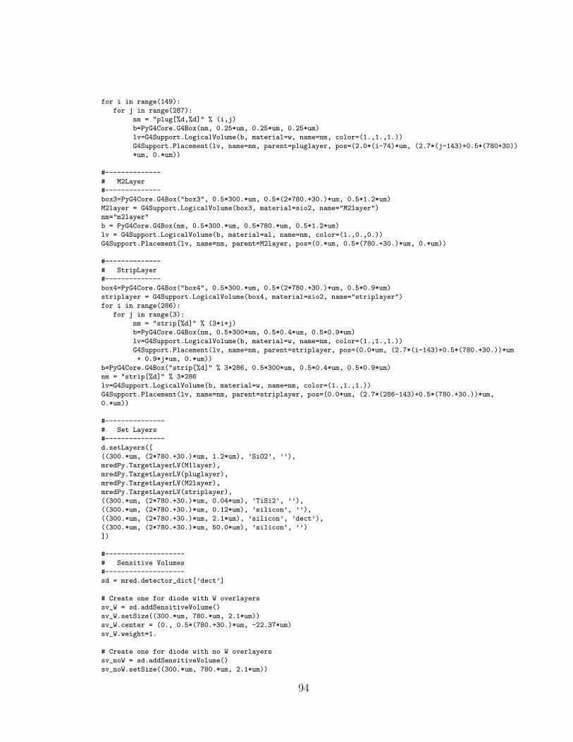
for i in range(149):for j in range(287):
nm = "plug[%d,%d]" % (i,j)b=PyG4Core.G4Box(nm, 0.25*um, 0.25*um, 0.25*um)lv=G4Support.LogicalVolume(b, material=w, name=nm, color=(1.,1.,1.))G4Support.Placement(lv, name=nm, parent=pluglayer, pos=(2.0*(i-74)*um, (2.7*(j-143)+0.5*(780+30))*um, 0.*um))
#--------------# M2Layer#--------------box3=PyG4Core.G4Box("box3", 0.5*300.*um, 0.5*(2*780.+30.)*um, 0.5*1.2*um)M2layer = G4Support.LogicalVolume(box3, material=sio2, name="M2layer")nm="m2layer"b = PyG4Core.G4Box(nm, 0.5*300.*um, 0.5*780.*um, 0.5*1.2*um)lv = G4Support.LogicalVolume(b, material=al, name=nm, color=(1.,0.,0.))G4Support.Placement(lv, name=nm, parent=M2layer, pos=(0.*um, 0.5*(780.+30.)*um, 0.*um))
#--------------# StripLayer#--------------box4=PyG4Core.G4Box("box4", 0.5*300.*um, 0.5*(2*780.+30.)*um, 0.5*0.9*um)striplayer = G4Support.LogicalVolume(box4, material=sio2, name="striplayer")for i in range(286):
for j in range(3):nm = "strip[%d]" % (3*i+j)b=PyG4Core.G4Box(nm, 0.5*300*um, 0.5*0.4*um, 0.5*0.9*um)lv=G4Support.LogicalVolume(b, material=w, name=nm, color=(1.,1.,1.))G4Support.Placement(lv, name=nm, parent=striplayer, pos=(0.0*um, (2.7*(i-143)+0.5*(780.+30.))*um+ 0.9*j*um, 0.*um))
b=PyG4Core.G4Box("strip[%d]" % 3*286, 0.5*300*um, 0.5*0.4*um, 0.5*0.9*um)nm = "strip[%d]" % 3*286lv=G4Support.LogicalVolume(b, material=w, name=nm, color=(1.,1.,1.))G4Support.Placement(lv, name=nm, parent=striplayer, pos=(0.0*um, (2.7*(286-143)+0.5*(780.+30.))*um,0.*um))
#---------------# Set Layers#---------------d.setLayers([((300.*um, (2*780.+30.)*um, 1.2*um), ’SiO2’, ’’),mredPy.TargetLayerLV(M1layer),mredPy.TargetLayerLV(pluglayer),mredPy.TargetLayerLV(M2layer),mredPy.TargetLayerLV(striplayer),((300.*um, (2*780.+30.)*um, 0.04*um), ’TiSi2’, ’’),((300.*um, (2*780.+30.)*um, 0.12*um), ’silicon’, ’’),((300.*um, (2*780.+30.)*um, 2.1*um), ’silicon’, ’dect’),((300.*um, (2*780.+30.)*um, 50.0*um), ’silicon’, ’’)])
#--------------------# Sensitive Volumes#--------------------sd = mred.detector_dict[’dect’]
# Create one for diode with W overlayerssv_W = sd.addSensitiveVolume()sv_W.setSize((300.*um, 780.*um, 2.1*um))sv_W.center = (0., 0.5*(780.+30.)*um, -22.37*um)sv_W.weight=1.
# Create one for diode with no W overlayerssv_noW = sd.addSensitiveVolume()sv_noW.setSize((300.*um, 780.*um, 2.1*um))
94
sv_noW.center = (0., -0.5*(780.+30.)*um, -22.37*um)sv_noW.weight=1.
d.register()
#------------------# Saving Histogram#------------------
mred.init()mred.accumulate_histograms=Truemred.setDefaultHistogram(options.histMin*MeV, options.histMax*MeV, 2000, options.histScale)
myFilePath = ’/home/clemenm1/SNL_Bulk_Diodes/hdf5_output/’
if batch_vars:if os.path.exists(myFilePath + batch_vars.runName):
print "\nOutput directory exists!"else:
os.mkdir(myFilePath + batch_vars.runName)print "\nOutput directory CREATED!"
mred.hdf5.file_path=str(myFilePath + batch_vars.runName)mred.hdf5.file_name=str(batch_vars.runName + "%03d.hdf5" % batch_vars.index)
else:if os.path.exists(myFilePath + options.runName):
print "\nOutput directory exists!"else:
os.mkdir(myFilePath + options.runName)print "\nOutput directory CREATED!"
mred.hdf5.file_path=str(myFilePath + options.runName)mred.hdf5.file_name=str(options.runName +’.hdf5’)
mred.hdf5.include_energies=Falsemred.hdf5.write_output_files=Truemred.hdf5.include_energies=Falsemred.hdf5.include_hits=Falsemred.hdf5.include_histograms=Truemred.hdf5.include_tracks=False
mred.gun.setParticle(options.particle)mred.gun.energy=options.beamE*MeV
mred.gun.random_spatial_sampling=’directionalFlux’mred.gun.random_use_device_radius=Falsemred.gun.random_box_size=waferSize
if options.gunDir==60:mred.gun.direction = (2,0,1)
if options.gunDir==85:mred.gun.direction = (11.43,0,1)
mred.progress_interval=options.nIons/100
if options.enableSUV:mred.suv()
mred.beamOn(options.nIons)
print "\nFluence Unit: ", mred.gun.fluence_unitprint "Beam Energy(MeV): ", options.beamEprint "Beam direction: ", options.gunDirprint "particle: ", options.particleprint "Hadronic Physics Model Selected: ", options.hadPhysprint "Hadronic Cross Section Multiplier: ", options.csMult
95

print "\n"
96
APPENDIX C
MRED SINGLE EVENT MODE EXAMPLE
CODE
This Appendix contains an example of Python code written to interface with
MRED version 9.2.0 on ACCRE in single event mode. The code simulates incident
particles (neutrons by default) incident on a 32⇥32 bit 65 nm SRAM using nested
sensitive volumes. The code records the weights SBU and MCU events to allow for
cross section calculations. Certain lines of code were too long for the page width and
were split to span two or more lines.
from PyG4Core import G4Colour as G4Colorimport base64import cPickleimport sysimport os
#----------------------------------------------# Option Parsing#----------------------------------------------from optparse import OptionParser
parser=OptionParser(usage="myScript [OPTIONS]")parser.disable_interspersed_args()# Options for runparser.add_option("", "--suv", action=’store_true’, dest="enableSUV", default=False, help="Use the GEANT4OpenGL viewer")
parser.add_option("", "--nIons", action=’store’, dest="nIons", type="int", default=100, help="The numberof particles to run. Default=100")parser.add_option("", "--particle", action=’store’, dest="particle", type="str", default="neutron", help="Particle species. Default=’neutron’ ")parser.add_option("", "--nspectrum", action=’store_true’, dest="nspectrum", default=False, help="Use the LANL neutron spectrum")parser.add_option("", "--jedecSpectrum", action=’store_true’, dest="jedecSpectrum", default=False, help="Use the JEDEC NYC neutron spectrum")parser.add_option("", "--triumfBL2C", action=’store_true’, dest="triumfBL2C", default=False, help="Usethe TRIUMF BL2C (up to 200 MeV) neutron spectrum")
parser.add_option("", "--beamE", action=’store’, dest="beamE", type="float", default=14.0, help="Beamenergy (MeV). Default=14")
parser.add_option("", "--beamZ", action=’store’, dest="beamZ", type="int", default=1, help="Beam atomicnumber")parser.add_option("", "--beamA", action=’store’, dest="beamA", type="int", default=1, help="Beam atomicweight")parser.add_option("", "--runName", action=’store’, dest="runName", type="str", default="test", help="File
97
name to save the hdf5 file. Default=’test’ ")parser.add_option("", "--rangeCuts", action=’store’, dest="rangeCuts", type="float", default=100.0, help="Physics Range Cuts in micrometers. Default=100")parser.add_option("", "--csMult", action=’store’, dest="csMult", type="float", default=400, help="HadronicCross Section Multiplier. Default 400")
parser.add_option("", "--gunDir", action=’store’, dest="gunDir", type="int", default=0, help="Direction ofincident beam in degrees. Default=0 (normal incidence)")
parser.add_option("", "--minE", action=’store’, dest="minE", type="float", default=1, help="Minimum Validtotal energy for each sd in keV. Default=1 keV")parser.add_option("", "--numRows", action=’store’, dest="numRows", type="int", default=32, help="Numberof rows in the SRAM. Default=32")
parser.add_option("", "--numCols", action=’store’, dest="numCols", type="int", default=32, help="Numberof columns in the SRAM. Default=32")parser.add_option("", "--tungsten", action=’store_true’, dest="tungsten", default=False, help="Puts a 0.3um thick W layer over the cell layer")
parser.add_option("", "--qcrit", action=’store’, dest="qcrit", type="float", default=1.0, help="Qcrit forReplay. Default 1.0 fC.")
#Physics List Optionsparser.add_option("", "--hadPhys", action=’store’, dest="hadPhys", type="str", default="CEM", help="Callsa certain hadronic physics model. Options are: ’CEM’, ’BinaryCascade’, ’BertiniCascade’, ’INCL_ABLA’,’G4QMD’, ’JQMD’ and ’PHITS’. Defaults to CEM, but goes to BertiniCascade if nothing else called.")
#Replay Optionsparser.add_option("", "--replaySeeds", action=’store’, dest="replaySeeds", type="str", default=None, help="Random Seeds for single replay")parser.add_option("", "--replayPickle", action=’store’, dest="replayPickle", type="str", default=None, help="File name for pickled list of random seeds")
(options, args) = parser.parse_args(run_args[1:])
class Device:’’’A class object representing a semiconductor device. A device consists of a name, critical energy,and a group of sensitive volumes. Each device maintains indices into an MRED sensitive volume listand its own energy deposition histogram. Although the device has an Ecrit, it does not filter eventsin the histogram. The entire energy deposition distribution is available for the user. The Ecrit isonly used to determine a coincident upset.’’’def __init__(self, name=None):
self.name=nameself.Ecrit=0.0self.sd=Noneself.group=Noneself.sv_idx_vector=[]
#---------------------------------------------# Define Physics#---------------------------------------------
PyG4Core.ExecuteCommand(’/control/verbose 2’)if mred.physics.list_name == ’PhysicsList’:# --------------------------------------------------------------------------# PenelopeQED is the default E&M model. Select one from the list.#mred.physics.addModule(’Standard’)mred.physics.addModule(’EmStandardScreened’)#mred.physics.addModule(’EmLowEnergyQED’)#mred.physics.addModule(’EmPenelopeQED’)# --------------------------------------------------------------------------# These are for elementary particles. Normally use them all.mred.physics.addModule(’HadronElastic’)mred.physics.addModule(’HadronInelastic’)mred.physics.addModule(’PiKInelastic’)#------------------------------------------------------------------# Hadronic Physics#------------------------------------------------------------------if options.hadPhys=="PHITS":
98
mred.physics.addModule(’NucleonHadronicPHITS’) # Experimentalelif options.hadPhys=="JQMD":mred.physics.addModule(’NucleonHadronicJQMD’) # Experimentalelse:mred.physics.addModule(’NucleonHadronic’)if options.hadPhys=="CEM":mred.physics.module_dict[’NucleonHadronic’].SetUseCEM(True)else:mred.physics.module_dict[’NucleonHadronic’].SetUseCEM(False)if options.hadPhys=="BinaryCascade":
mred.physics.module_dict[’NucleonHadronic’].SetUseBinaryCascade(True)elif options.hadPhys=="G4QMD":mred.physics.module_dict[’NucleonHadronic’].SetProtonsUseQMD(True)elif options.hadPhys=="INCL_ABLA":mred.physics.module_dict[’NucleonHadronic’].SetUseInclAblaCascade(True)#mred.physics.module_dict[’NucleonHadronic’].SetInclAblaUseStrictEnergyLimit(True)else:mred.physics.module_dict[’NucleonHadronic’].SetUseBertiniCascade()if options.hadPhys != ’BertiniCascade’: print "***Hadronic Physics not valid, using Bertini Cascade***"mred.physics.module_dict[’NucleonHadronic’].SetUseHPNeutrons(True)# --------------------------------------------------------------------------# Ion Nuclear Physics#-------------------------------------------------------------------------# ’AltIonInelastic’ is the default ion-ion model## The following are for using G4QMD#mred.physics.addModule(’IonInelasticG4QMD’)# The following can be used together to pick the FRAG model to replace GEM.# This is a one-way choice. It is not possible to go back to GEM.#mred.physics.module_dict[’IonInelasticG4QMD’].GetG4QMDModel().UnUseGEM()#mred.physics.module_dict[’IonInelasticG4QMD’].GetG4QMDModel().UseFRAG()#mred.physics.addModule(’IonInelastic’)#mred.physics.addModule(’AltIonInelastic’)#mred.physics.addModule(’IonInelasticJQMD’)#mred.physics.addModule(’IonInelasticPHITS’)#mred.physics.addModule(’IonInelasticLAQGSM’)#mred.physics.addModule(’IonAbrasion’)#mred.physics.addModule(’IonAbrasionEMD’)# --------------------------------------------------------------------------mred.physics.module_dict[’Decay’].SetIncludeRadioactiveDecay(False)# --------------------------------------------------------------------------# These can be used to turn on and set the threshold for Penelope transport.#mred.physics.module_dict[’StandardScreened’].SetUsePenelope(True)#mred.physics.module_dict[’StandardScreened’].SetPenelopeThreshold(50.*keV)# ------------------------------------------------------------------------------# These commands set up the cross section biasing wrapper. They will only have# an effect on processes defined by Geant4 reference physics lists if those# processes have been explicitly wrapped.mred.physics.use_multiplier_primary_only=Truemred.physics.use_track_weighting=Trueprint "cross_section_wrapper_info = %s" % mred.physics.cross_section_wrapper_info
#------------# Range Cuts#------------mred.physics.range_cuts = options.rangeCuts*1.0*um
#-------------------------# Cross Section Multiplier#-------------------------mred.physics.hadronic_cross_section_multiplier = options.csMult
################################################################################ Create a layered device
99
###############################################################################d=mred.setDevice(’rpp’)mred.materials.enableBasicElectronicMaterials()mred.materials.enableMaterial(’air’)
if options.tungsten: mred.materials.enableMaterial(’tungsten’)
# Create the layered device for an array of devices. This stack is created to# include extra material around the array. Because of this, the sensitive# detector is not the entire width of the silicon layer. I have also omitted# the oxide material for STI instead lumping it into the silicon layer. This# will hopefully avoid the boundary stepping problem with energy deposition# seen in other simulations.
# A list of semiconductor devicesdeviceList=[]
layers = []nCols=options.numColsnRows=options.numRowsscalingParameter=1
margin=20.0substrateDepth=10cellWidth=0.975*scalingParametercellLength=0.475*scalingParameterlayerWidth=(nCols * cellWidth + margin) * micrometerlayerLength=(nRows * cellLength + margin) * micrometerprint "Cell Size %g x %g" % ( cellWidth, cellLength )
#A solid block of Si with a W layer next to the sensitive volumes.if options.tungsten:layers.append(((layerWidth, layerLength, 4.19*micrometer), ’silicon’))layers.append(((layerWidth, layerLength, 0.3*micrometer), ’tungsten’))else:layers.append(((layerWidth, layerLength, 4.49*micrometer), ’silicon’))
layers.append(((nCols * cellWidth*micrometer, nRows * cellLength*micrometer, 5.0*micrometer), ’silicon’,’default’))
layers.append(((layerWidth, layerLength, substrateDepth*micrometer), ’silicon’))d.setLayers(layers)d.wafer_material=’silicon’
mred.device.register(d.g4PV())mred.init()
sd = mred.sd_vector[0]print "Configuring sensitive detector %s" % ( sd.name )mred.runAct.SetAutoGenerateHistogramsFlag(False)mred.accumulate_histograms=False
# Create each device as a group of associated sensitive volumeszoffset=(d.wafer_dimensions[2]/um / 2.0) - (substrateDepth+5.0)
# According to Jeff Black, the columns are divided into 16 groups of 32.# Each of bit in a 16-bit word is then separated by 32 columns. If a# checkerboard pattern is written to the array, there will be blocks of# 0’s and 1’s. In that sense, we are always simulated all 0’s or all 1’s.# Also, although the cells are mirrored, the sense amp polarities run the same# way therefore assume that a logic 0 results in a sensitive volume on the# left of the cell and a logic 1 results in a sensitive volume on the right.# Finally, assume that the block cells being simulated are the least# significant bit.nwellWidth=0.368*scalingParameterpwellWidth=0.607*scalingParameter
100
pattern=int(’0xAAAA’,16)for row in range(nRows):
for col in range(nCols):device=Device(’r%d_c%d’ % (row, col))device.group=sd.addSensitiveVolume(’group’)device.group.on=Truedevice.group.weight=1device.Ecrit=device.group.min_valid_total_energy=0.*keV
data=pattern&1evenRow=bool(row%2)evenCol=bool(col%2)# Calculate the extremes of the cellcellXmin = (col*cellWidth) - (nCols*cellWidth)/2.0cellXcenter = (col*cellWidth) - (nCols*cellWidth)/2.0 + cellWidth/2.0cellXmax = (col*cellWidth) - (nCols*cellWidth)/2.0 + cellWidthcellYmin = (row*cellLength) - (nRows*cellLength)/2.0cellYcenter = (row*cellLength) - (nRows*cellLength)/2.0 + cellLength/2.0cellYmax = (row*cellLength) - (nRows*cellLength)/2.0 + cellLength# Calculated the center of the sensitive volume based on data, column,# and row.if data == 0:
xoffset = cellXmin + 0.15*scalingParameterelse:
xoffset = cellXmax - 0.15*scalingParameterif evenRow:
yoffset = cellYmax - 0.237*scalingParameter # 0.2else:
yoffset = cellYmin + 0.237*scalingParameter
depth = 0.450*scalingParameter# Calibrated for TAMU N LET = 0.6 ~ 550 MeVsv=device.group.add(’rpp’)sv.setCenter(vector3d(xoffset,yoffset,zoffset+depth/2.0)*micrometer)sv.setSize(vector3d(0.110*scalingParameter,0.140*scalingParameter,depth*scalingParameter)*micrometer)sv.on=Truesv.weight=0.75 # 0.70sv.cpp_sv.SetDisplayColour(PyG4Core.G4Colour(0,1,0,min(1,sv.weight)))
# Calibrated for LBNL B LET = 0.89 ~ 105 MeVsv=device.group.add(’rpp’)sv.setCenter(vector3d(xoffset,yoffset,zoffset+depth/2.0)*micrometer)sv.setSize(vector3d(0.110*scalingParameter,0.180*scalingParameter,depth)*micrometer)sv.on=Truesv.weight=0.23 # 0.23sv.cpp_sv.SetDisplayColour(PyG4Core.G4Colour(0,1,0,min(1,sv.weight)))
# Calibrated for TAMU Ne LET = 2.8 ~ 250 MeVsv=device.group.add(’rpp’)sv.setCenter(vector3d(xoffset,cellYcenter,zoffset+depth/2.0)*micrometer)sv.setSize(vector3d(0.11*scalingParameter,cellLength+0.1,depth)*micrometer)sv.on=Truesv.weight=0.07 # 0.07sv.cpp_sv.SetDisplayColour(PyG4Core.G4Colour(0,1,0,min(1,sv.weight)))
# Guess for PMOSsv=device.group.add(’rpp’)sv.setCenter(vector3d(cellXcenter,cellYcenter,zoffset+depth/2.0)*micrometer)sv.setSize(vector3d(0.088*scalingParameter,cellLength,depth)*micrometer)sv.on=Truesv.weight=0.07 # 0.07sv.cpp_sv.SetDisplayColour(PyG4Core.G4Colour(0,1,0,min(1,sv.weight)))
101
# Pwell# 1um at 0.07 give FIT ~240, but ion is 4e-9, or 0.75um at 0.09, or 0.6 at 0.116depth2=0.475*scalingParametersv=device.group.add(’rpp’)if data == 0:
sv.setCenter(vector3d(cellXmin+0.05,cellYcenter,zoffset+depth+depth2/2.0)*micrometer)else:
sv.setCenter(vector3d(cellXmax-0.05,cellYcenter,zoffset+depth+depth2/2.0)*micrometer)sv.setSize(vector3d(pwellWidth-0.1,cellLength,depth2)*micrometer) # 0.2sv.on=Truesv.weight=0.07 # 0.10 7 0.02sv.cpp_sv.SetDisplayColour(PyG4Core.G4Colour(0,1,0,min(1,sv.weight)))
# Nwell# 1um at 0.07 give FIT ~240, but ion is 4e-9, or 0.75um at 0.09, or 0.6 at 0.116depth2=0.475*scalingParametersv=device.group.add(’rpp’)sv.setCenter(vector3d(cellXcenter,cellYcenter,zoffset+depth+depth2/2.0)*micrometer)sv.setSize(vector3d(nwellWidth,cellLength,depth2)*micrometer) # 0.2sv.on=Truesv.weight=0.07 # 0.10 7 0.02sv.cpp_sv.SetDisplayColour(PyG4Core.G4Colour(0,1,0,min(1,sv.weight)))
depth3=0.5*scalingParametersv=device.group.add(’rpp’)sv.setCenter(vector3d(cellXcenter,cellYcenter,zoffset+depth+depth2+depth3/2.0)*micrometer)sv.setSize(vector3d(cellWidth,cellLength,depth3)*micrometer) # 0.2sv.on=Truesv.weight=0.02 # 0.10 7sv.cpp_sv.SetDisplayColour(PyG4Core.G4Colour(0,1,0,min(1,sv.weight)))
deviceList.append(device)
# This is really only enabled for efficiency. We don’t want to enter the single# event callback for every particle, so putting a small, but meaningful filter# here will help a lot. If the model has been calibrated, this should be set# just below the critical energy.sd.use_weighted_as_total=Truesd.min_valid_total_energy=options.minE*keV
#-------------# Saving File#-------------
myFilePath = ’/home/clemenm1/MBU/Output/’
if batch_vars:if os.path.exists(myFilePath + batch_vars.runName):
print "\nOutput directory exists!"else:
os.mkdir(myFilePath + batch_vars.runName)print "\nOutput directory CREATED!"
file_name=str(myFilePath + batch_vars.runName + "/" + batch_vars.runName + "%03d.pickle" %batch_vars.index)text_file_name=str(myFilePath + batch_vars.runName + "/" + batch_vars.runName + "%03d.txt" %batch_vars.index)else:
if os.path.exists(myFilePath + options.runName):print "\nOutput directory exists!"
else:os.mkdir(myFilePath + options.runName)
print "\nOutput directory CREATED!"file_name=str(myFilePath + options.runName + "/" + options.runName + ".pickle")
text_file_name=str(myFilePath + options.runName + "/" + options.runName + ".txt")
102
#--------# SCU & MCU processing variables#-------
global SCU_sum, MCU2_sum, MCU3_sum, MCU4_sum, MCU5_sum, MCU6p_sumglobal SCU_num, MCU2_num, MCU3_num, MCU4_num, MCU5_num, MCu6p_num, SCU_xlistSize = int((50-0)/0.1)SCU_sum = [0]*listSize; MCU2_sum = [0]*listSize; MCU3_sum = [0]*listSize; MCU4_sum = [0]*listSize;MCU5_sum = [0]*listSize; MCU6p_sum = [0]*listSizeSCU_num = [0]*listSize; MCU2_num = [0]*listSize; MCU3_num = [0]*listSize; MCU4_num = [0]*listSize;MCU5_num = [0]*listSize; MCU6p_num = [0]*listSizeSCU_x = [0]*listSize
#-------# Particle beam#-------
mred.gun.random_energy_sampling=’uniform’mred.gun.random_spatial_sampling=’directionalFlux’mred.gun.random_use_device_radius=False
if options.nspectrum:#measured neutron flux at LANSCEmred.gun.setEnergySpectrumFile(’/usr/local/radeffects/data/environments/LANL_neutrons/nLANLENormand.dat’)elif options.jedecSpectrum:mred.gun.setEnergySpectrumFile(’/usr/local/radeffects/data/environments/NYC_neutrons/NYC_neutron_flux.dat’)elif options.triumfBL2C:#FLUKA calculation of neutron flux in BL2C beamlinemred.gun.setEnergySpectrumFile(’/home/clemenm1/local/TRIUMF_BL2C_nFlux.dat’)else:mred.gun.energy=options.beamE*MeV
mred.gun.setParticle(options.particle)
mred.gun.random_box_size=d.wafer_dimensions
if options.gunDir==60:mred.gun.direction = (2,0,1)elif options.gunDir==85:mred.gun.direction = (11.43,0,1)else:mred.gun.direction = (0,0,1)
mred.progress_interval=options.nIons/100#mred.include_particles="True"
if options.enableSUV:mred.suv()
############### Write File Headers#############
if options.replayPickle:pickOutFile = options.replayPickle + "_replayedEvents.txt"FILE = open(pickOutFile, ’w’)else:FILE = open(text_file_name, ’w’)#FILE.write("For each event - Random Seeds, SV index and Charge collected above 1 keV in a %i x %i SVmatrix with 65nm SV dim:\n" % (nCols, nRows) )
def singleEventCallback(evt):#I want to save:
103
# 1. all the charge coll events with the index of the SV.# 2. the random seeds for each event# 3. weight (variance is weight^2 so no need to record it)# 4. the processed data - pickle file
global deviceList, SCU_sum, MCU2_sum, MCU3_sum, MCU4_sum, MCU5_sum, MCU6p_sum, SCU_num, MCU2_num,MCU3_num, MCU4_num, MCU5_num, MCU6p_num
randomSeeds=mred.last_random_seedsweight = mred.evtAct.ComputeEventWeight(evt)
if (options.replaySeeds or options.replayPickle):myTrackDict = mred.evtAct.get_track_dict(evt)
for i in range(1,len(myTrackDict) + 1):particle_name = myTrackDict[i].GetParticleName()initial_kinetic_energy = myTrackDict[i].GetInitialKineticEnergy()LET = mred.LET(particle_name, ’silicon’, initial_kinetic_energy)angle = math.degrees(myTrackDict[i].GetInitialMomentumDirection().getTheta())if LET > 0.5:
if options.replayPickle:if (angle > 30):
FILE.write("\nNeutron E: %0.1f, Particle: %s, Energy:%0.1f, LET: %0.2f, angle: %0.1f "%(myTrackDict[1].GetInitialKineticEnergy(),particle_name, initial_kinetic_energy, LET, angle))
else:print "Particle #%i: %s, angle: %0.1f, Energy: %0.1f,LET: %0.2f" %(i, particle_name, angle,initial_kinetic_energy, LET)
sys.stdout.flush()
Qs=[0]*len(deviceList)aboveCharge=0for i in range(len(deviceList)):
Qs[i] = deviceList[i].group.total_energy/0.0225if Qs[i] > 0.04: # 1 keV
if options.replaySeeds:# print SV index with charge collectedprint "(%i, %.2f)," % (i,Qs[i])
else:# write SV index with charge collectedFILE.write("(%i, %.2f)," % (i,Qs[i]))
aboveCharge+=1
if aboveCharge>0:myTrackDict = mred.evtAct.get_track_dict(evt)nEnergy = initial_kinetic_energy = myTrackDict[1].GetInitialKineticEnergy()if options.replaySeeds:
print "Random Seeds: (%d, %d), weight: %0.2e, En: %0.2f" %(randomSeeds[0],randomSeeds[1], weight, nEnergy)
else:#write random seeds and weight and neutron EnergyFILE.write("(%d, %d),%0.2e,E%0.2e\n" % (randomSeeds[0], randomSeeds[1],weight, nEnergy))
qi=0qf=50qstep=0.1qloops=int((qf-qi)/qstep)
for j in xrange(qloops):good=0qcrit=j*qstep+qifor i in range(len(deviceList)):
104
if(Qs[i] > qcrit):good += 1
SCU_x[j] = qcrit
if(good == 1):SCU_sum[j] += weightSCU_num[j] += 1
elif(good == 2):MCU2_sum[j] += weightMCU2_num[j] += 1
elif(good == 3):MCU3_sum[j] += weightMCU3_num[j] += 1
elif(good == 4):MCU4_sum[j] += weightMCU4_num[j] += 1
elif(good == 5):MCU5_sum[j] += weightMCU5_num[j] += 1
elif(good > 5):MCU6p_sum[j] += weightMCU6p_num[j] += 1
sys.stdout.flush()
################################################################################# Filters################################################################################if options.particle == "neutron":
mred.filter.on=Truemred.filter.verbose=Falsemred.filter.include_particles=Truemred.filter.include_scatters=Truemred.filter.include_nuclear_elastic=Truemred.filter.include_coulomb_elastic=True
if options.replaySeeds:print "Replaying event %s" % (options.replaySeeds)mred.random_seeds=eval(options.replaySeeds)mred.runSingleEventMode(1,function=singleEventCallback)
elif options.replayPickle:print "Replaying seeds from file: %s" %(options.replayPickle)ofileName = options.replayPickle + ".pickle"ofile = open(ofileName, ’r’)pickleSeeds=cPickle.load(ofile)ofile.close()for i in range(len(pickleSeeds)):
nextSeeds=(pickleSeeds[i][0], pickleSeeds[i][1])mred.random_seeds=nextSeedsmred.runSingleEventMode(1, function=singleEventCallback)
else:mred.runSingleEventMode(options.nIons,function=singleEventCallback)
FILE.close()
print "\nFluence Unit: ", mred.gun.fluence_unitif options.nspectrum:
print "LANL neutron spectrum used"print "Spectrum Integral: ", mred.gun.energy_spectrum.spectrum.integral()
elif options.jedecSpectrum:print "JEDEC NYC neutron spectrum used"print "Spectrum Integral: ", mred.gun.energy_spectrum.spectrum.integral()
elif options.triumfBL2C:print "TRIUMF BL2C neutron spectum used"print "Spectrum Integral: ", mred.gun.energy_spectrum.spectrum.integral()
105
else:print "Beam Energy(MeV): ", options.beamE
print "Beam direction: ", options.gunDirprint "particle: ", options.particleprint "Hadronic Physics Model Selected: ", options.hadPhysprint "Hadronic Cross Section Multiplier: ", options.csMultprint "\n"
q=int(options.qcrit*10)print "SCU_sum: ", SCU_sum[q], "SCU_num: ", SCU_num[q]print "2CU_sum: ", MCU2_sum[q], "MCU2_num: ", MCU2_num[q]print "3CU_sum: ", MCU3_sum[q], "MCU3_num: ", MCU3_num[q]print "4CU_sum: ", MCU4_sum[q], "MCU4_num: ", MCU4_num[q]print "5CU_sum: ", MCU5_sum[q], "MCU5_num: ", MCU5_num[q]print "6pCU_sum: ", MCU6p_sum[q], "MCU6p_num: ", MCU6p_num[q]
data = {"SCU_sum": SCU_sum, "SCU_num": SCU_num,"MCU2_sum": MCU2_sum, "MCU2_num": MCU2_num,"MCU3_sum": MCU3_sum, "MCU3_num": MCU3_num,"MCU4_sum": MCU4_sum, "MCU4_num": MCU4_num,"MCU5_sum": MCU5_sum, "MCU5_num": MCU5_num,"MCU6p_sum": MCU6p_sum, "MCU6p_num": MCU6p_num,"SCU_x": SCU_x}
pickleFile=open(file_name, ’w’)cPickle.dump(data, pickleFile)pickleFile.close()
106
BIBLIOGRAPHY
[1] G. E. Moore, “Cramming more components onto integrated circuits,” Electron-ics, vol. 38, Apr 1965.
[2] J. Wallmark and S. Marcus, “Minimum size and maximum packing density ofnonredundant semiconductor devices,” Proc. of the IRE, vol. 50, pp. 286–298,1962.
[3] D. Binder, E. Smith, and A. Holman, “Satellite anomalies from galactic cosmicions,” IEEE Trans. on Nucl. Sci., vol. NS-22, no. 6, pp. 2675–2680, 1975.
[4] T. May and M. Woods, “Alpha-particle-induced soft errors in dynamic memo-ries,” IEEE Trans. on Elec. Dev., vol. ED-26, no. 1, pp. 2–9, 1979.
[5] C. Howe, R. Weller, R. Reed, M. Mendenhall, R. Schrimpf, K. Warren, D. Ball,L. Massengill, K. LaBel, J. Howard, and N. Haddad, “Role of heavy-ion nuclearreactions in determining on-orbit single event error rates,” Nuclear Science, IEEETransactions on, vol. 52, pp. 2182–2188, Dec 2005.
[6] J. Schwank, M. Shaneyfelt, J. Baggio, P. Dodd, J. Felix, V. Ferlet-Cavrois,P. Paillet, D. Lambert, F. Sexton, G. Hash, and E. Blackmore, “E↵ects of particleenergy on proton-induced single-event latchup,” Nuclear Science, IEEE Trans-actions on, vol. 52, pp. 2622–2629, Dec 2005.
[7] P. Goldhagen, J. M. Clem, and J. Wilson, “The energy spectrum of cosmic-rayinduced neutrons measured on an airplane over a wide range of altitude andlatitude,” Radiation Protection Dosimetry, vol. 110, pp. 387–392, Aug 2004.
[8] E. Normand, “Single event upset at ground level,” IEEE Trans. Nucl. Sci.,vol. 43, pp. 2742–2750, Dec 1996.
[9] J. Baggio, V. Ferlet-Cavrois, and D. Lambert, “Neutron and proton-inducedsingle event upsets in advanced commercial fully depleted soi srams,” NuclearScience, Jan 2006.
[10] S. P. Platt, A. V. Prokofiev, and C. X. Xiao, “Fidelity of energy spectra atneutron facilities for single-event e↵ects testing,” IEEE Inter. Rel. Phys. Symp.,pp. 411–415, May 2010.
[11] C. Dyer, A. Hands, K. Ford, A. Frydland, and P. Truscott, “Neutron-inducedsingle event e↵ects testing across a wide range of energies and facilities andimplications for standards,” IEEE Trans. Nucl. Sci., vol. 53, pp. 3596–3601, Dec2006.
107
[12] E. Normand and L. Dominik, “Cross comparison guide for results of neutronsee testing of microelectronics applicable to avionics,” Radiation E↵ects DataWorkshop (REDW), 2010 IEEE, p. 8, 2010.
[13] M. Martone, M. Angelone, and M. Pillon, “The 14 mev frascati neutron gener-ator,” J. Nucl. Mat., pp. 1661–1664, Jan 1994.
[14] M. A. Clemens, N. C. Hooten, V. Ramachandran, N. A. Dodds, R. A. Weller,M. H. Mendenhall, R. A. Reed, P. E. Dodd, M. R. Shaneyfelt, J. R. Schwank,and E. W. Blackmore, “The e↵ect of high-z materials on proton-induced chargecollection,” IEEE Trans. Nucl. Sci., vol. 57, pp. 3212–3218, Dec 2010.
[15] M. Clemens, B. Sierawski, K. Warren, M. Mendenhall, N. Dodds, R. Weller,R. Reed, P. Dodd, M. Shaneyfelt, J. Schwank, S. Wender, and R. Baumann,“The e↵ects of neutron energy and high-z materials on single event upsets andmultiple cell upsets,” IEEE Trans. Nucl. Sci., vol. 58, no. 6, pp. 2591 – 2598,2011.
[16] J. Barth, C. Dyer, and E. Stassinopoulos, “Space, atmospheric, and terrestrial ra-diation environments,” Nuclear Science, IEEE Transactions on, vol. 50, pp. 466– 482, Jun 2003.
[17] F. W. Sexton, “Measurement of single event phenomena in devices and ics,”IEEE NSREC Short Course, New Orleans, LA, 1992.
[18] E. G. Stassinopoulos, “Microelectronics for the natural radiation environmentsof space,” IEEE NSREC Short Course, 1990.
[19] J. L. Barth, “Applying computer simulation tools to radiation e↵ects problem,”IEEE NSREC Short Course, 1997.
[20] C. S. Dyer, “Radiation e↵ects in the new millennium—old realities and newissues,” IEEE NSREC Short Course, 1998.
[21] J. Mazur, “Radiation e↵ects—from particles to payloads,” IEEE NSREC ShortCourse, 2002.
[22] J. F. Ziegler, “Terrestrial cosmic rays,” IBM J. Res. Development, vol. 40, no. 1,pp. 19–39, 1996.
[23] “Creme96: Cosmic ray e↵ects on micro electronics website (1997). [online]. cur-rently available at https://creme.isde.vanderbilt.edu/.”
[24] “Measurement and reporting of alpha particle and terrestrial cosmic ray-inducedsoft errors in semiconductor devices,” JEDEC Standard - JESD89A, Oct 2006.
[25] H. Barnaby, “Total-ionizing-dose e↵ects in modern cmos technologies,” IEEETrans. Nucl. Sci., vol. 53, pp. 3103–3121, Jan 2006.
108
[26] J. Srour, C. J. Marshall, and P. W. Marshall, “Review of displacement damagee↵ects in silicon devices,” IEEE Trans. Nucl. Sci., vol. 50, pp. 653–670, Jan 2003.
[27] P. E. Dodd and L. W. Massengill, “Basic mechanisms and modeling of single-event upset in digital microelectronics,” IEEE Trans. Nucl. Sci., vol. 50, pp. 583–602, Jan 2003.
[28] T. Holman, “Radiation hardening techniques for analog and mixed-signal inte-grated circuits.” From EECE 304 class lecture, 2008.
[29] R. Baumann, “The impact of technology scaling on soft error rate performanceand limits to the e�cacy of error correction,” Proc. Int. Electron Device Meeting,pp. 329–332, 2002.
[30] R. L. Pease, “Total-dose issues for microelectronics in space systems,” IEEETrans. Nucl. Sci., vol. 43, no. 2, pp. 442–452, 1996.
[31] A. R. Frederickson, “Upsets related to spacecraft charging,” IEEE Trans. Nucl.Sci., vol. 43, no. 2, pp. 426–441, 1996.
[32] J. Ziegler, “Stopping of energetic light ions in elemental matter,” Journal ofApplied Physics, Jan 1999.
[33] W. Shockley, “Problems related to p-n junctions in silicon,” Solid State Electron,vol. 2, pp. 35–67, 1961.
[34] N. Dodds, R. Reed, M. Mendenhall, R. Weller, M. Clemens, P. Dodd,M. Shaneyfelt, G. Vizkelethy, J. Schwank, V. Ferlet-Cavrois, J. Adams,R. Schrimpf, and M. King, “Charge generation by secondary particles from nu-clear reactions in beol materials,” IEEE Trans. Nucl. Sci., vol. 56, pp. 3172 –3179, Dec 2009.
[35] L. Massengill, “Practical considerations in applying electronics to space sys-tems,” IEEE NSREC Short Course, 1992.
[36] K. Warren, “Sensitive volume models for single event upset analysis and rateprediction for space, atmospheric, and terrestrial radiation environments,” Ph.D.Dissertation, Jun 2010.
[37] R. Lacoe, “Radiation e↵ects in advanced commercial technologies: How devicescaling has a↵ected the selection of spaceborne electronics,” IEEE NSREC ShortCourse, 2003.
[38] P. Dodd, “Radiation e↵ects in the space telecom environment: Ii. basic mecha-nisms for single-event e↵ects,” IEEE NSREC Short Course, 1999.
109
[39] M. McMahan, “The berkeley accelerator space e↵ects (base) facility – a newmission for the 88-inch cyclotron at lbnl,” Nuclear Instruments and Methods inPhysics Research B, vol. 241, pp. 409–413, Nov 2005.
[40] “http://cyclotron.tamu.edu/.”
[41] C. C. Foster, S. L. Casey, A. L. Johnson, P. Miesle, N. Sifri, A. H. Skees, andK. M. Murray, “Opportunities for single event and other radiation e↵ects testingand research at the indiana university cyclotron facility,” IEEE Radiation E↵ectsData Workshop, pp. 84–87, Mar 1996.
[42] “Test procedures for the measurement of single-event e↵ects in semiconductordevices from heavy ion irradiation,” JESD57, Oct 1996.
[43] R. A. Weller, M. H. Mendenhall, R. A. Reed, R. D. Schrimpf, K. M. Warren,B. D. Sierawski, and L. W. Massengill, “Monte carlo simulation of single evente↵ects,” IEEE Trans. Nucl. Sci., vol. 57, pp. 1726–1746, Aug 2010.
[44] S. Buchner, J. Langworthy, W. Stapor, A. B. Campbell, and S. Rivet, “Impli-cations of the spatial dependence of the single-event-upset threshold in sramsmeasured with a pulsed laser,” IEEE Trans. Nucl. Sci., vol. 41, no. 6, pp. 2195– 2202, 1994.
[45] K. Warren, L. Massengill, R. Schrimpf, and H. Barnaby, “Analysis of the influ-ence of mos device geometry on predicted seu cross sections,” IEEE Trans. Nucl.Sci, vol. 46, no. 6, pp. 1363 – 1369, 1999.
[46] B. Sierawski, J. Pellish, R. Reed, R. Schrimpf, K. Warren, R. Weller, M. Menden-hall, J. Black, A. Tipton, M. Xapsos, R. Baumann, X. Deng, M. Campola,M. Friendlich, H. Kim, A. Phan, and C. Seidleck, “Impact of low-energy protoninduced upsets on test methods and rate predictions,” IEEE Trans. Nucl. Sci.,vol. 56, no. 6, pp. 3085 – 3092, 2009.
[47] B. D. Sierawski, K. M. Warren, R. A. Reed, R. A. Weller, M. M. Mendenhall,R. D. Schrimpf, R. C. Baumann, and V. Zhu, “Contribution of low-energy ( 10mev) neutrons to upset rate in a 65 nm sram,” IEEE Inter. Rel. Phys. Symp.,pp. 395 – 399, 2010.
[48] N. Seifert, B. Gill, and K. Foley. . . , “Multi-cell upset probabilities of 45nm high-k+ metal gate sram devices in terrestrial and space environments,” IEEE Inter-national Reliability Physics Symposium (IRPS), Jan 2008.
[49] A. Tipton, J. Pellish, R. Reed, R. Schrimpf, R. Weller, M. Mendenhall, B. Sier-awski, A. Sutton, R. Diestelhorst, G. Espinel, J. Cressler, P. Marshall, andG. Vizkelethy, “Multiple-bit upset in 130 nm cmos technology,” IEEE Trans.Nucl. Sci., vol. 53, no. 6, pp. 3259 – 3264, 2006.
110
[50] A. Kobayashi, D. Ball, K. Warren, R. Reed, N. Haddad, M. Mendenhall,R. Schrimpf, and R. Weller, “The e↵ect of metallization layers on single eventsusceptibility,” Nuclear Science, IEEE Transactions on, vol. 52, no. 6, pp. 2189– 2193, 2005.
[51] R. A. Reed, R. A. Weller, R. D. Schrimpf, M. H. Mendenhall, K. M. Warren,and L. W. Massengill, “Implications of nuclear reactions for single event e↵ectstest methods and analysis,” IEEE Trans. Nucl. Sci., vol. 53, pp. 3356–3362, Dec2006.
[52] P. J. McNulty, G. E. Farrell, and W. P. Tucker, “Proton-induced nuclear reac-tions in silicon,” Nuclear Science, IEEE Transactions on, vol. 28, pp. 4007–4012,Dec 1981.
[53] P. J. McNulty, “Microelectronics for the natural radiation environments ofspace,” IEEE NSREC Short Course, 1990.
[54] R. Reed, R. Weller, M. Mendenhall, J.-M. Lauenstein, K. Warren, J. Pellish,R. Schrimpf, B. Sierawski, L. Massengill, P. Dodd, M. Shaneyfelt, J. Felix,J. Schwank, N. Haddad, R. Lawrence, J. Bowman, and R. Conde, “Impact ofion energy and species on single event e↵ects analysis,” IEEE Trans. Nucl. Sci.,vol. 54, pp. 2312–2321, Dec 2007.
[55] K. Warren, B. Sierawski, R. Reed, R. Weller, C. Carmichael, A. Lesea,M. Mendenhall, P. Dodd, R. Schrimpf, L. Massengill, T. Hoang, H. Wan, J. D.Jong, R. Padovani, and J. Fabula, “Monte-carlo based on-orbit single event up-set rate prediction for a radiation hardened by design latch,” IEEE Trans. Nucl.Sci., vol. 54, pp. 2419–2425, Dec 2007.
[56] K. Pomorski and J. Dudek, “Nuclear liquid-drop model and surface-curvaturee↵ects,” Phys. Rev. C, vol. 67, p. 044316, Jan 2003.
[57] B. A. Brown and B. H. Wildenthal, “Status of the nuclear shell model,” Ann.Rev. Nucl. Part. Sci., vol. 38, pp. 29–66, Jan 1988.
[58] G. R. Satchler, “Introduction to nuclear reactions,” John Wiley & Sons, 1980.
[59] S. Mongelli, J. Maiorino, S. Anefalos, A. Deppman, and T. Carluccio, “Spallationphysics and the ads target design,” Bra. J. of Phys., vol. 35, no. 3B, pp. 894–897,2005.
[60] W. G. Lynch, “Nuclear fragmentation in proton- and heavy-ion-induced reac-tions,” Annual Review of Nuclear and Particle Science, vol. 37, no. 1, pp. 493–535, 1987.
111
[61] V. Viola, K. Kwiatkowski, L. Beaulieu, D. Bracken, H. Breuer, J. Brzychczyk,R. de Souza, D. Ginger, W.-C. Hsi, R. Korteling, T. Lefort, W. Lynch, K. Mor-ley, R. Legrain, L. Pienkowski, E. Pollacco, E. Renshaw, A. Ruangma, M. Tsang,C. Volant, G. Wang, S. Yennello, and N. Yoder, “Light-ion-induced multifrag-mentation: The isis project,” Physics Reports, vol. 434, no. 1-2, pp. 1 – 46,2006.
[62] A. V. Prokofiev, “Compilation and systematics of proton-induced fission cross-section data,” Nuclear Instruments and Methods in Physics Research SectionA: Accelerators, Spectrometers, Detectors and Associated Equipment, vol. 463,no. 3, pp. 557 – 575, 2001.
[63] V. Karnaukhov, “Nuclear multifragmentation and phase transitions in hot nu-clei,” Physics of Particles and Nuclei, Jan 2006.
[64] N. A. Dodds, “Charge generation by secondary particles from nuclear reactionsin back end of line materials,” Master’s Thesis, Dec 2009.
[65] J. Ziegler, “Srim-2003,” Nuclear Inst. and Methods in Physics Research, Jan2004.
[66] P. E. Dodd, F. W. Sexton, and P. S. Winokur, “Three-dimensional simulation ofcharge collection and multiple-bit upset in si devices,” IEEE TRANSACTIONSON NUCLEAR SCIENCE, vol. 41, pp. 2005–2017, Dec 1994.
[67] J. Allison et al., “Geant4 developments and applications,” Nuclear Science, IEEETransactions on, vol. 53, pp. 270–278, Feb 2006.
[68] M. H. Mendenhall and R. A. Weller, “A probability-conserving cross-section bi-asing mechanism for monte-carlo variance reduction with application to geant4,”Nucl. Inst. Meth. Phys. Res. A, vol. 667, pp. 38–43, Jan 2012.
[69] M. Sabra, R. Weller, M. Mendenhall, R. Reed, M. Clemens, and A. Barghouty,“Validation of nuclear reaction codes for proton-induced radiation e↵ects: Thecase for cem03,” IEEE Trans. Nucl. Sci., vol. 58, no. 6, pp. 3134 – 3138, 2011.
[70] M. S. Sabra, M. A. Clemens, R. A. Weller, M. H. Mendenhall, A. F. Bargh-outy, and F. B. Malik, “Validation of nuclear reaction models of 180mev proton-induced fragmentation of 27al,” Nucl. Inst. Meth. Phys. Res., B, vol. 269,pp. 2463–2468, Nov 2011.
[71] S. Mashnik, A. Sierk, K. Gudima, and M. Baznat, “Cem03 and laqgsm03—newmodeling tools for nuclear applications,” J. Phys: Conf. Ser., vol. 41, pp. 340–351, Jan 2006.
[72] K. Niita, T. Sato, H. Iwase, H. Nose, and H. Nakashima, “Phits—a particle andheavy ion transport code system,” Rad. Meas., vol. 41, pp. 1080–1090, Jan 2006.
112
[73] S. G. Mashnik, “Validation and verification of mcnp6 against intermediate andhigh-energy experimental data and results by other codes,” International Con-ference on Mathematics and Computational Methods Applied to Nuclear Scienceand Engineering (M&C 2011) Rio de Janeiro, RJ, Brazil, May 8-12, 2011, pp. 1–15, Nov 2011.
[74] R. A. Reed, P. W. Marshall, H. S. Kim, P. J. McNulty, B. Fodness, T. M. Jordan,R. Reedy, C. Tabbert, M. S. T. Liu, W. Heikkila, S. Buchner, R. Ladbury, andK. A. LaBel, “Evidence for angular e↵ects in proton-induced single-event upsets,”IEEE Trans. Nucl. Sci., vol. 49, pp. 3038–3044, Dec 2002.
[75] A. Tipton, X. Zhu, H. Weng, J. Pellish, P. Fleming, R. Schrimpf, R. Reed,R. Weller, and M. Mendenhall, “Increased rate of multiple-bit upset from neu-trons at large angles of incidence,” IEEE Trans. Dev. Mat. Rel., vol. 8, no. 3,pp. 565 – 570, 2008.
[76] T. Merelle, F. Saigne, B. Sagnes, G. Gasiot, P. Roche, T. Carriere, M.-C. Palau,F. Wrobel, and J.-M. Palau, “Monte-carlo simulations to quantify neutron-induced multiple bit upsets in advanced srams,” IEEE Trans. Nucl. Sci., vol. 52,pp. 1538–1544, Dec 2005.
[77] A. N. Smirnov, V. P. Eismont, N. P. Filatov, J. Blomgren, H. Conde, A. V.Prokofiev, P.-U. Renberg, and N. Olsson, “Measurements of neutron-inducedfission cross sections for 209bi, natpb, 208pb, 197au, natw, and 181ta in theintermediate energy region,” Phys. Rev. C, vol. 70, p. 054603, Nov 2004.
[78] N. F. Haddad, A. T. Kelly, R. K. Lawrence, B. Li, J. C. Rodgers, J. F. Ross,K. M. Warren, R. A. Weller, M. H. Mendenhall, and R. A. Reed, “Incrementalenhancement of seu hardened 90 nm cmos memory cell,” IEEE Trans. Nucl. Sci.,vol. 58, pp. 975–980, Jun 2011.
[79] E. Normand, “Extensions of the burst generation rate method for wider appli-cation to proton/neutron-induced single event e↵ects,” IEEE Trans. Nucl. Sci.,vol. 45, no. 6, pp. 2904 – 2914, 1998.
[80] M. Chadwick, P. Oblozinsky, M. Herman, N. Greene, R. McKnight, D. Smith,P. Young, R. MacFarlane, G. Hale, S. Frankle, A. Kahler, T. Kawano, R. Lit-tle, D. Madland, P. Moller, R. Mosteller, P. Page, P. Talou, H. Trellue,M. White, W. Wilson, R. Arcilla, C. Dunford, S. Mughabghab, B. Pritychenko,D. Rochman, A. Sonzogni, C. Lubitz, T. Trumbull, J. Weinman, D. Brown,D. Cullen, D. Heinrichs, D. McNabb, H. Derrien, M. Dunn, N. Larson, L. Leal,A. Carlson, R. Block, J. Briggs, E. Cheng, H. Huria, M. Zerkle, K. Kozier,A. Courcelle, V. Pronyaev, and S. C. vanderMarck, “Endf/b-vii.0: Next genera-tion evaluated nuclear data library for nuclear science and technology,” NuclelarData Sheets, vol. 107, pp. 2931–3060, Dec 2006.
113
[81] G. Gasiot, D. Giot, and P. Roche, “Multiple cell upsets as the key contributionto the total ser of 65 nm cmos srams and its dependence on well engineering,”IEEE Trans. Nucl. Sci., vol. 54, no. 6, pp. 2468 – 2473, 2007.
[82] N. Bohr Phil. Mag., vol. 21, p. 212, 1913.
[83] H. Bethe Ann. Physik, vol. 5, p. 325, 1930.
[84] H. Bethe Z. Phys., vol. 76, p. 293, 1932.
[85] J. F. Ziegler, J. P. Biersack, and U. Littmark, The Stopping and Range of Ionsin Solids, vol. 1. 1985.
[86] U. Fano, “Penetration of protons, alpha particles, and mesons,” Annual Reviewof Nuclear Science, Jan 1963.
[87] S. Ahlen, “Theoretical and experimental aspects of the energy loss of relativisticheavily ionizing particles,” Rev. of Mod. Phys., vol. 52, no. 1, pp. 121–173, 1980.
[88] P. Sigmund, R. Bimbot, H. Geissel, H. Paul, and A. Schinner, “Stopping of ionsheavier than helium,” ICRU Report 73. J. of the ICRU, vol. 5, pp. 1–235, 2005.
[89] H. Bishel Phys. Rev. A, vol. 41, p. 3642, 1990.
[90] F. Allegrini, D. J. McComas, D. T. Young, J.-J. Berthelier, J. Covinhes, J.-M.Illiano, J.-F. Riou, H. O. Funsten, and R. W. Harper, “Energy loss of 1-50 kevh, he, c, n, o, ne, and ar ions transmitted through thin carbon foils,” Review ofScientific Instruments, vol. 77, no. 4, p. 044501, 2006.
114