ENE 334 Microprocessors -...
36
ENE 334 Microprocessors Page 1 Lecture 7: MCS-51 Architecture I http://webstaff.kmutt.ac.th/~dejwoot.kha/ Week #07 : Dejwoot KHAWPARISUTH
Transcript of ENE 334 Microprocessors -...
ENE 334 Microprocessors
Page 1
Lecture 7:
MCS-51 Architecture I
http://webstaff.kmutt.ac.th/~dejwoot.kha/
Week #07 : Dejwoot KHAWPARISUTH

Outlines:
Page 2
➔ 8051 Microcontroller Hardware
➔ Input/Output Pins, Ports, and Circuits
➔ External Memory ➔ Counters and Timers ➔ Serial Data I/O ➔ Interrupts
Week #07 ENE 334 MCS-51 Architecture I
Reference: Textbooks
Page 3
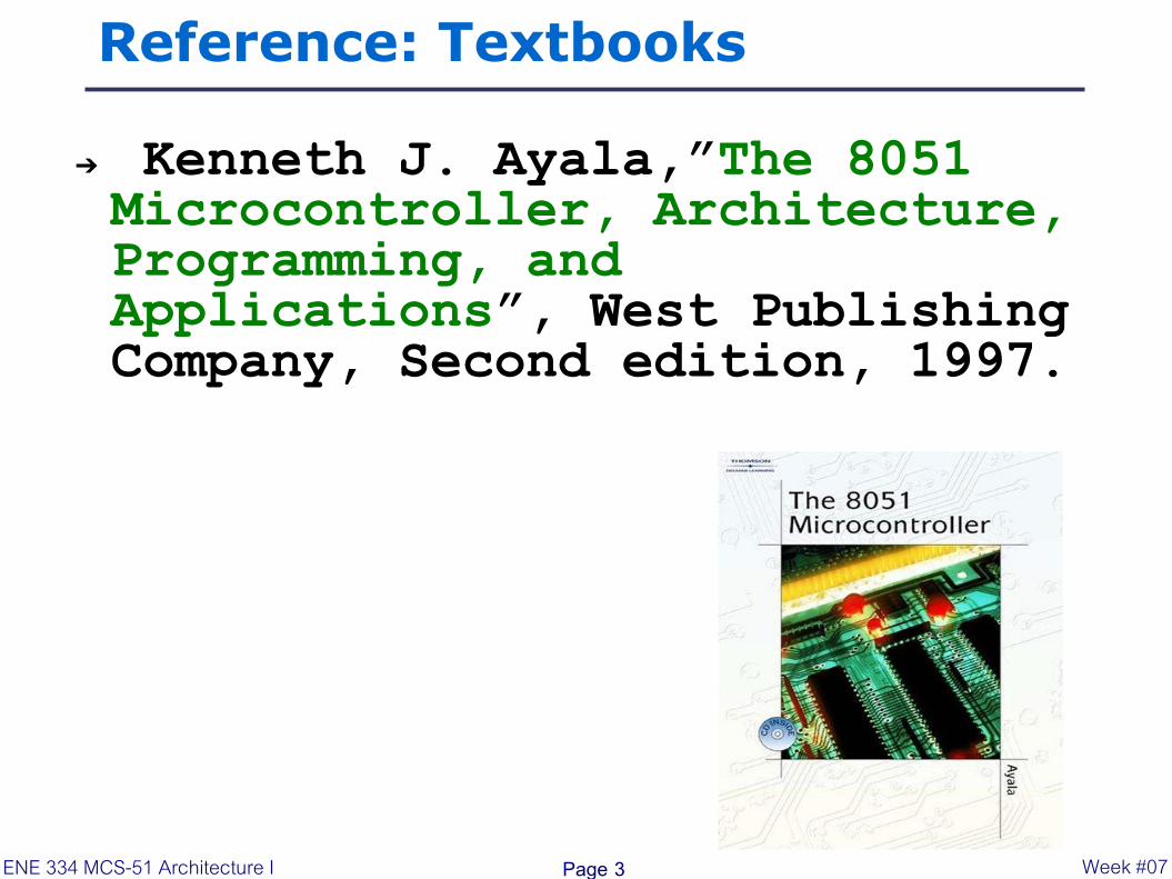
➔ Kenneth J. Ayala,”The 8051 Microcontroller, Architecture, Programming, and Applications”, West Publishing Company, Second edition, 1997.
ENE 334 MCS-51 Architecture I Week #07

Reference:
Page 4
➔ MCS@51 MICROCONTROLLER FAMILY USER’S MANUAL”, Intel, February 1994.
ENE 334 MCS-51 Architecture I Week #07
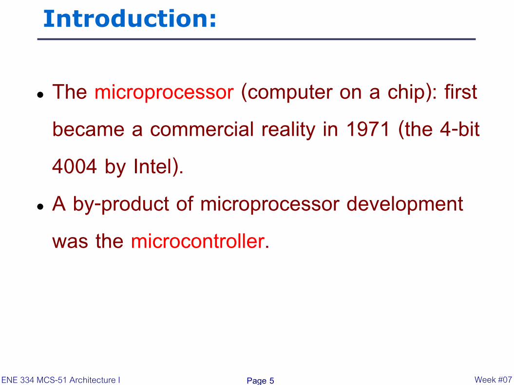
Introduction:
Page 5
● The microprocessor (computer on a chip): first became a commercial reality in 1971 (the 4-bit 4004 by Intel).
● A by-product of microprocessor development was the microcontroller.
ENE 334 MCS-51 Architecture I Week #07
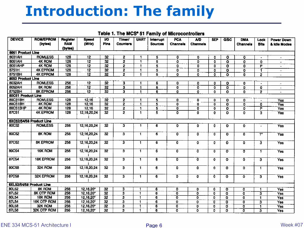
Introduction: The family
Page 6 ENE 334 MCS-51 Architecture I Week #07

Introduction: The family
Page 7 ENE 334 MCS-51 Architecture I Week #07
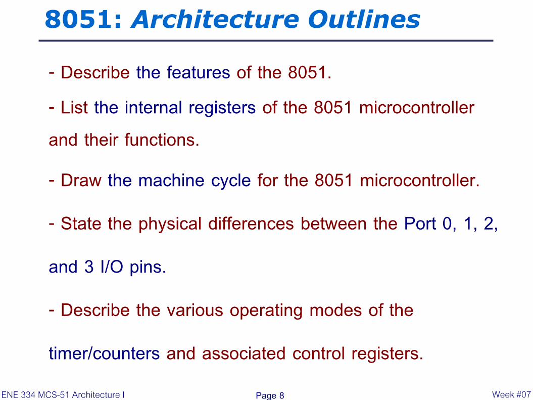
8051: Architecture Outlines
Page 8
- Describe the features of the 8051. - List the internal registers of the 8051 microcontroller and their functions.
- Draw the machine cycle for the 8051 microcontroller.
- State the physical differences between the Port 0, 1, 2,
and 3 I/O pins.
- Describe the various operating modes of the
timer/counters and associated control registers.
ENE 334 MCS-51 Architecture I Week #07

8051: Architecture Outlines
Page 9
- Describe the various operating modes of the
UART(Universal Asynchronous Recevier Transmitter), and
associated control registers.
- List the types of interrupts, the interrupt program
addresses, and the interrupt control registers.
ENE 334 MCS-51 Architecture I Week #07
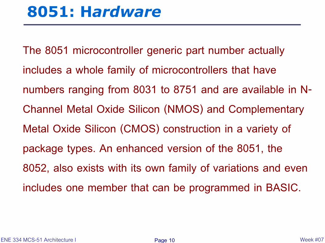
8051: Hardware
Page 10
The 8051 microcontroller generic part number actually includes a whole family of microcontrollers that have numbers ranging from 8031 to 8751 and are available in N-Channel Metal Oxide Silicon (NMOS) and Complementary Metal Oxide Silicon (CMOS) construction in a variety of package types. An enhanced version of the 8051, the 8052, also exists with its own family of variations and even includes one member that can be programmed in BASIC.
ENE 334 MCS-51 Architecture I Week #07

8051: Hardware
Page 11
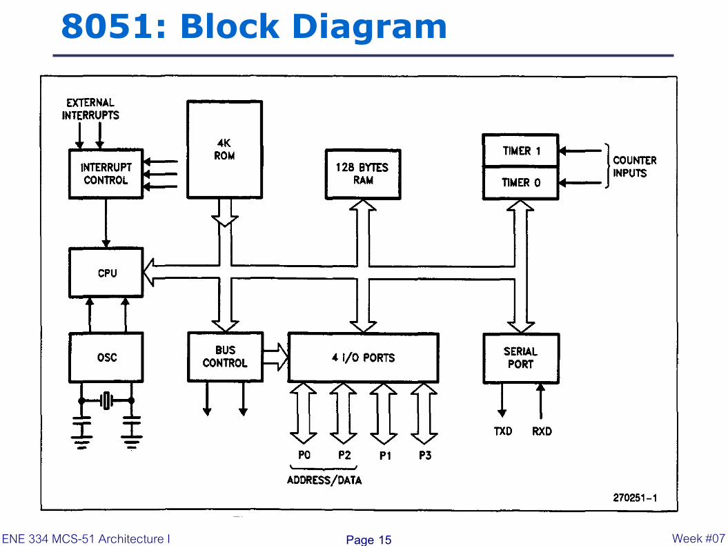
We will study a “generic” 8051, housed in a 40-pin DIP,
and direct the investigation of a particular type to the data
books. The block diagram of the 8051 in Figure shows all
of the features unique to microcontrollers:
ENE 334 MCS-51 Architecture I Week #07
8051: features
Page 12
- Eight-bit CPU optimized for control applications with registers A (the accumulator) and B - Extensive Boolean processing capabilities - Sixteen-bit program counter (PC) and data pointer (DPTR) - 64K Program Memory address space - 64K Data Memory address space - Eight-bit program status word (PSW) - Eight-bit stack pointer (SP) - Internal ROM or EPROM (8751) of 0 (8031) to 4K (8051)
ENE 334 MCS-51 Architecture I Week #07
8051: features
Page 13
- Internal RAM of 128 bytes: - Four register banks, each containing eight registers - Sixteen bytes, which may be addressed at the bit level - Eighty bytes of general-purpose data memory - Thirty-two input/output pins arranged as four 8-bit ports: P0—P3 - Two 16-bit timer/counters: T0 and T1
ENE 334 MCS-51 Architecture I Week #07

8051: features
Page 14
- Full duplex serial data receiver/transmitter: SBUF
- Control registers: TCON, TMOD, SCON, PCON, IP, and IE
- Two external and three internal interrupt sources
(6-source/5-vector interrupt structure with two prioritylevels)
- Oscillator and clock circuits (on-chip)
ENE 334 MCS-51 Architecture I Week #07
8051: Block Diagram
Page 15 ENE 334 MCS-51 Architecture I Week #07
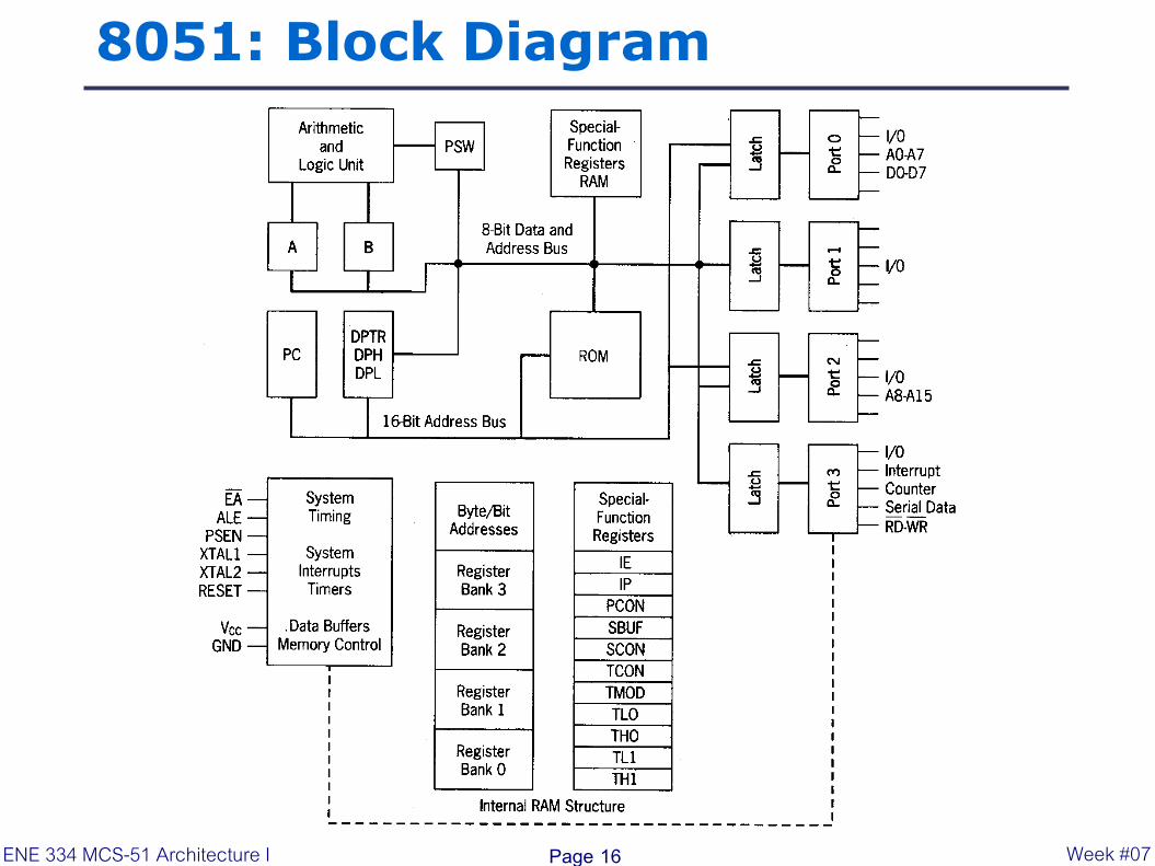
8051: Block Diagram
Page 16 ENE 334 MCS-51 Architecture I Week #07
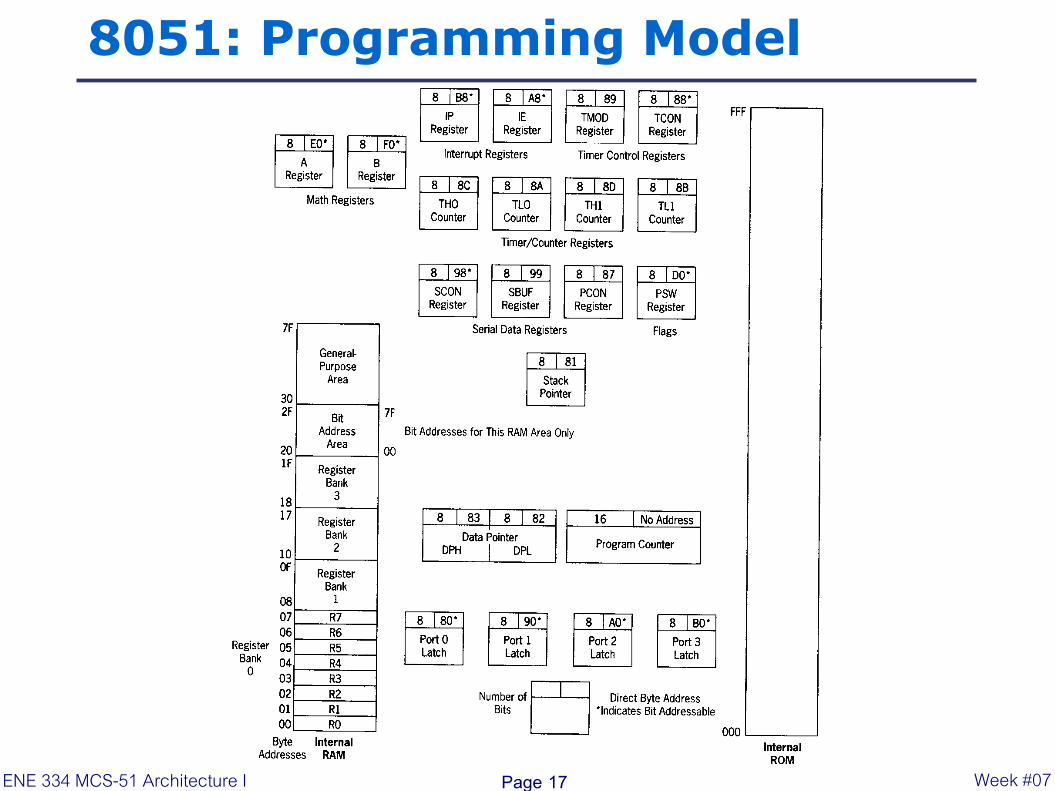
8051: Programming Model
Page 17 ENE 334 MCS-51 Architecture I Week #07
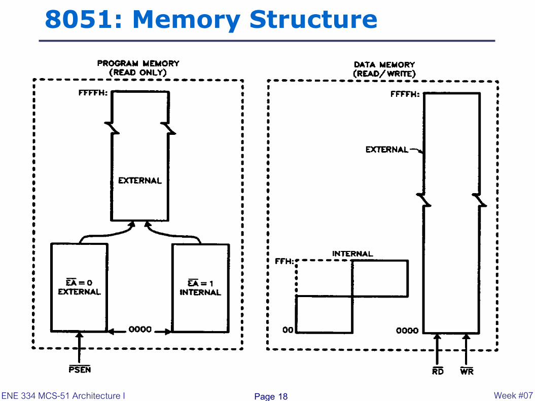
8051: Memory Structure
Page 18 ENE 334 MCS-51 Architecture I Week #07
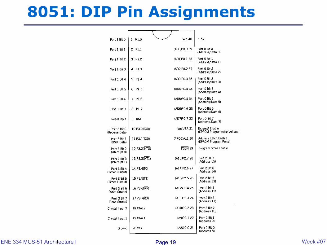
8051: DIP Pin Assignments
Page 19 ENE 334 MCS-51 Architecture I Week #07

8051: Oscillator & Timing
Page 20 ENE 334 MCS-51 Architecture I Week #07
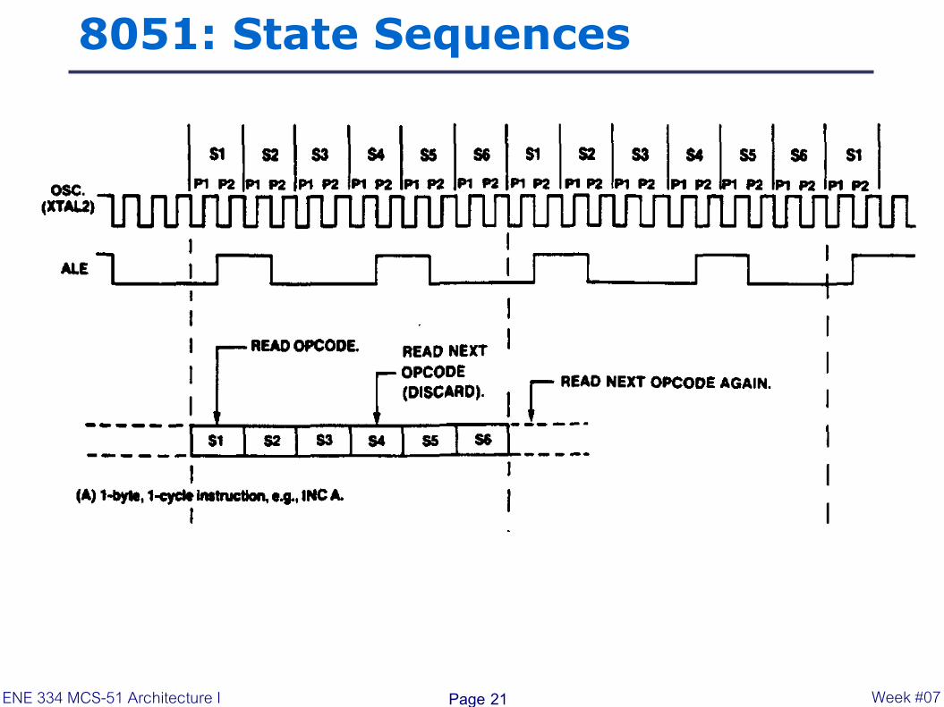
8051: State Sequences
Page 21 ENE 334 MCS-51 Architecture I Week #07

8051: State Sequences
Page 22 ENE 334 MCS-51 Architecture I Week #07
8051: Oscillator & Clock
Page 23
The manufacturers make available 8051 designs that can
run at specified maximum and minimum frequencies,
typically 1 megahertz to 16 megahertz. Minimum
frequencies imply that some internal memories are dynamic
and must always operate above a minimum frequency or
data will be lost.
ENE 334 MCS-51 Architecture I Week #07
8051: Oscillator & Clock
Page 24
The clock frequency, f, establishes the smallest interval of time within the microcontroller, called the pulse, P, time. The smallest interval of time to accomplish any simple instruction, or part of a complex instruction, however, is the machine cycle. The machine cycle is itself made up of six states. A state is the basic time interval for discrete operations of the microcontroller such as fetching an opcode byte, decoding an opcode, executing an opcode, or writing a data byte. Two oscillator pulses define each state.
ENE 334 MCS-51 Architecture I Week #07
8051: Oscillator & Clock
Page 25
Program instructions may require one, two, or four machine
cycles to be executed, depending on the type of instruction.
Instructions are fetched and executed by the
microcontroller automatically, beginning with the instruction
located at ROM memory address 0000h at the time the
microcontroller is first reset.
ENE 334 MCS-51 Architecture I Week #07
8051: Oscillator & Clock
Page 26
Note: there are two ALE pulses per machine cycle. The ALE pulse, which is primarily used as a timing pulse for external memory access, indicates when every instruction byte is fetched. Two bytes of a single instruction may thus be fetched, and executed, in one machine cycle. Single byte instructions are not executed in a half cycle, however. Single-byte instructions “throw-away” the second byte (which is the first byte of the next instruction.) The next instruction is then fetched in the following cycle.
ENE 334 MCS-51 Architecture I Week #07
8051: SFR
Page 27
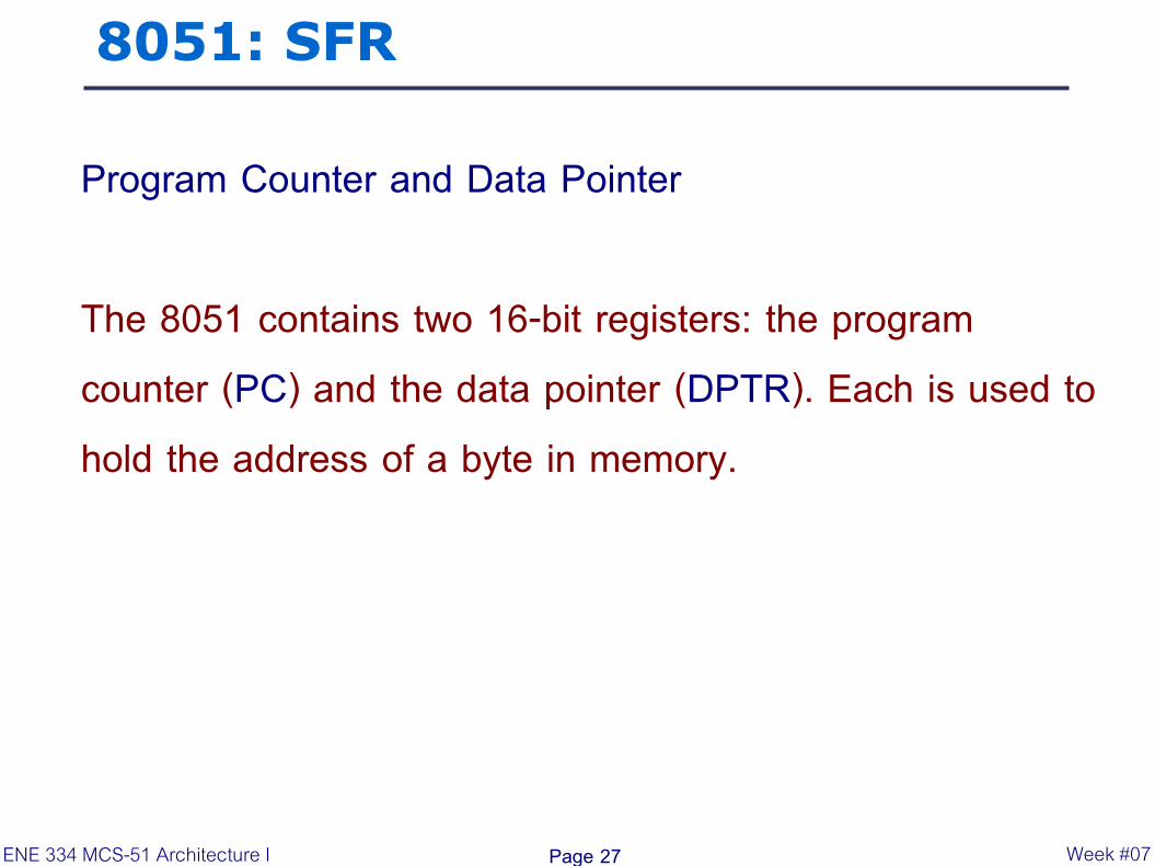
Program Counter and Data Pointer The 8051 contains two 16-bit registers: the program counter (PC) and the data pointer (DPTR). Each is used to hold the address of a byte in memory.
ENE 334 MCS-51 Architecture I Week #07

8051: SFR
Page 28
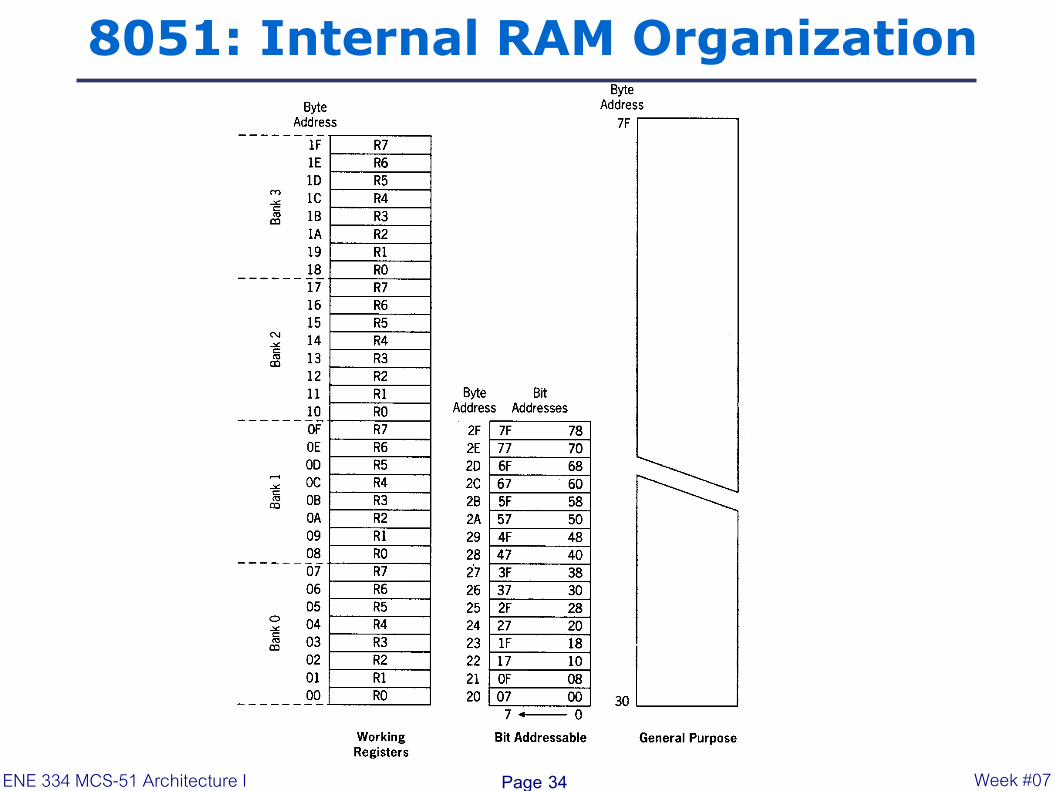
A and B CPU Registers The 8051 contains 34 general-purpose, or working, registers. Two of these, registers A and B, hold results of many instructions, particularly math and logical operations, of the 8051 central processing unit (CPU). The other 32 are arranged as part of internal RAM in four banks, B0—B3, of eight registers and comprise the mathematical core.
ENE 334 MCS-51 Architecture I Week #07
8051: SFR
Page 29
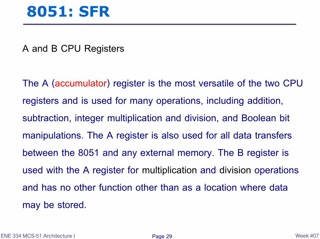
A and B CPU Registers The A (accumulator) register is the most versatile of the two CPU registers and is used for many operations, including addition, subtraction, integer multiplication and division, and Boolean bit manipulations. The A register is also used for all data transfers between the 8051 and any external memory. The B register is used with the A register for multiplication and division operations and has no other function other than as a location where data may be stored.
ENE 334 MCS-51 Architecture I Week #07

8051: SFR
Page 30
Flags and the Program Status Word (PSW) Flags are 1-bit registers provided to store the results of certain program instructions. Other instructions can test the condition of the flags and make decisions based on the flag states. In order that the flags may be conveniently addressed, they are grouped inside the program status word (PSW) and the power control (PCON) registers.
ENE 334 MCS-51 Architecture I Week #07

8051: PSW
Page 31 ENE 334 MCS-51 Architecture I Week #07

8051: PSW
Page 32
The PSW contains the math flags, user program flag F0, and the register select bits that identify which of the four general-purpose register banks is currently in use by the program. The remaining two user flags, GF0 and GF1, are stored in PCON. The math flags include Carry (C), Auxiliary Carry (AC), Overflow (OV), and Parity (P). User flags are general-purpose flags that may be used by the programmer to record some event in the program.
ENE 334 MCS-51 Architecture I Week #07
8051: SFR
Page 33
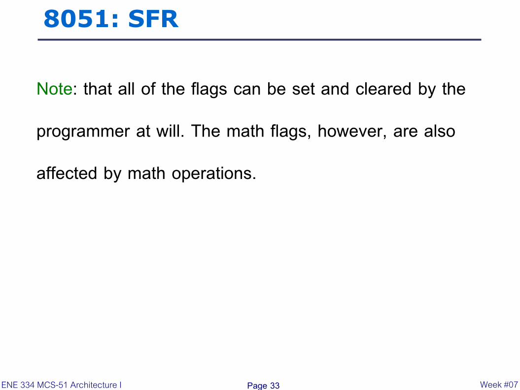
Note: that all of the flags can be set and cleared by the
programmer at will. The math flags, however, are also
affected by math operations.
ENE 334 MCS-51 Architecture I Week #07
8051: Internal RAM Organization
Page 34 ENE 334 MCS-51 Architecture I Week #07

8051: Internal RAM Organization
Page 35
Unlike microcontrollers with Von Neumann architectures,
which can use a single memory address for either program
code or data, but not for both, the 8051 has a Harvard
architecture, which uses the same address, in different
memories, for code and data. Internal circuitry accesses
the correct memory based on the nature of the operation in
progress.
ENE 334 MCS-51 Architecture I Week #07

To be continued:
Page 36 ENE 334 MCS-51 Architecture I Week #07