EN / ACS880 diode supply control program firmware …...Diode supply module Diode (or...
194
ABB industrial drives Firmware manual ACS880 diode supply control program
Transcript of EN / ACS880 diode supply control program firmware …...Diode supply module Diode (or...

ABB industrial drives
Firmware manualACS880 diode supply control program

List of related manuals
You can find manuals and other product documents in PDF format on the Internet. See section Document library on the Internet on the inside of the back cover. For manuals not available in the Document library, contact your local ABB representative.
General manuals Code (English)
Safety instructions for ACS880 multidrive cabinets and modules 3AUA0000102301
Safety instructions for ACS880 liquid-cooled multidrive cabinets and modules
3AXD50000048633
Electrical planning instructions for ACS880 multidrive cabinets and modules
3AUA0000102324
Electrical planning instructions for ACS880 liquid-cooled multidrive modules
3AXD50000048634
Mechanical installation instructions for ACS880 multidrive cabinets 3AUA0000101764
Cabinet design and construction instructions for ACS880 air-cooled and liquid-cooled multidrive modules
3AUA0000107668
Inverter module manuals and guides
ACS880-104 inverter modules hardware manual 3AUA0000104271
ACS880-104LC inverter modules hardware manual 3AXD50000045610
ACS880 primary control program firmware manual 3AUA0000085967
ACS880 primary control program quick start-up guide 3AUA0000098062
Supply module manuals
ACS880-204 IGBT supply modules hardware manual 3AUA0000131525
ACS880 IGBT supply control program firmware manual 3AUA0000131562
ACS880-304 +A003 diode supply modules hardware manual 3AUA0000102452
ACS880-304 +A018 diode supply modules hardware manual 3AXD50000010104
ACS880-304LC+A019 diode supply modules hardware manual 3AXD50000045157
ACS880 diode supply control program firmware manual 3AUA0000103295
ACS880 distributed I/O bus supplement 3AXD50000126880
ACS880-904 regenerative rectifier modules hardware manual 3AXD50000020457
ACS880 regenerative rectifier control program firmware manual 3AXD50000020827
Brake module and DC/DC converter module manuals
ACS880-604 1-phase brake chopper units as modules hardware manual
3AUA0000106244
ACS880-604 3-phase brake modules hardware manual 3AXD50000022033
ACS880 brake control program firmware manual 3AXD50000020967
ACS880-1604 DC/DC converter modules hardware manual 3AXD50000023642
ACS880 DC/DC converter control program firmware manual 3AXD50000024671
Cabinet-installed multidrive manuals
ACS880-107 inverter units hardware manual 3AUA0000102519
ACS880-207 IGBT supply units hardware manual 3AUA0000130644
ACS880-307 (+A003) diode supply units hardware manual 3AUA0000102453
ACS880-307 +A018 diode supply units hardware manual 3AXD50000011408
ACS880-607 1-phase brake units hardware manual 3AUA0000102559
ACS880-607 3-phase brake units hardware manual 3AXD50000022034
ACS880-907 regenerative rectifier units hardware manual 3AXD50000020546
ACS880-1607 DC/DC converter units hardware manual 3AXD50000023644
Option manuals and guides
ACX-AP-x assistant control panels user’s manual 3AUA0000085685

Firmware manual
ACS880 diode supply control program
3AUA0000103295 Rev FEN
EFFECTIVE: 2017-06-09
2017 ABB Oy. All Rights Reserved.
2. Start-up
Table of contents

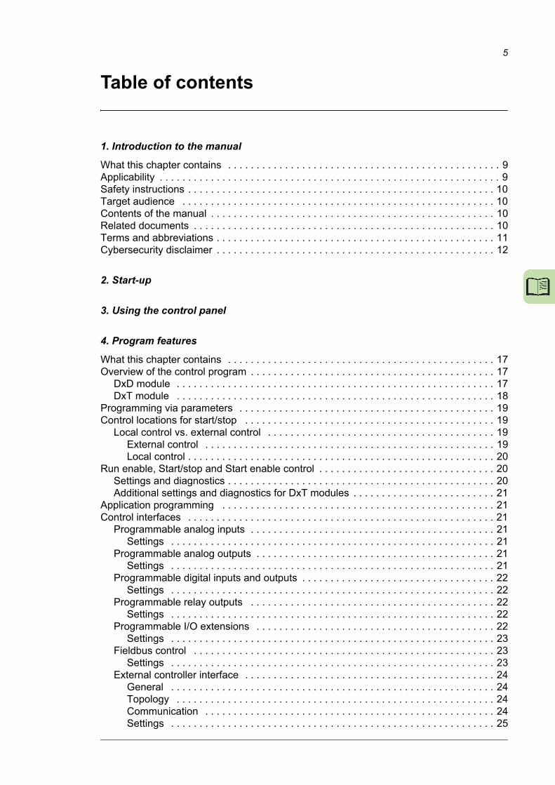
5
Table of contents
1. Introduction to the manual
What this chapter contains . . . . . . . . . . . . . . . . . . . . . . . . . . . . . . . . . . . . . . . . . . . . . . . . 9Applicability . . . . . . . . . . . . . . . . . . . . . . . . . . . . . . . . . . . . . . . . . . . . . . . . . . . . . . . . . . . . 9Safety instructions . . . . . . . . . . . . . . . . . . . . . . . . . . . . . . . . . . . . . . . . . . . . . . . . . . . . . . 10Target audience . . . . . . . . . . . . . . . . . . . . . . . . . . . . . . . . . . . . . . . . . . . . . . . . . . . . . . . 10Contents of the manual . . . . . . . . . . . . . . . . . . . . . . . . . . . . . . . . . . . . . . . . . . . . . . . . . . 10Related documents . . . . . . . . . . . . . . . . . . . . . . . . . . . . . . . . . . . . . . . . . . . . . . . . . . . . . 10Terms and abbreviations . . . . . . . . . . . . . . . . . . . . . . . . . . . . . . . . . . . . . . . . . . . . . . . . . 11Cybersecurity disclaimer . . . . . . . . . . . . . . . . . . . . . . . . . . . . . . . . . . . . . . . . . . . . . . . . . 12
2. Start-up
3. Using the control panel
4. Program features
What this chapter contains . . . . . . . . . . . . . . . . . . . . . . . . . . . . . . . . . . . . . . . . . . . . . . . 17Overview of the control program . . . . . . . . . . . . . . . . . . . . . . . . . . . . . . . . . . . . . . . . . . . 17
DxD module . . . . . . . . . . . . . . . . . . . . . . . . . . . . . . . . . . . . . . . . . . . . . . . . . . . . . . . . 17DxT module . . . . . . . . . . . . . . . . . . . . . . . . . . . . . . . . . . . . . . . . . . . . . . . . . . . . . . . . 18
Programming via parameters . . . . . . . . . . . . . . . . . . . . . . . . . . . . . . . . . . . . . . . . . . . . . 19Control locations for start/stop . . . . . . . . . . . . . . . . . . . . . . . . . . . . . . . . . . . . . . . . . . . . 19
Local control vs. external control . . . . . . . . . . . . . . . . . . . . . . . . . . . . . . . . . . . . . . . . 19External control . . . . . . . . . . . . . . . . . . . . . . . . . . . . . . . . . . . . . . . . . . . . . . . . . . . 19Local control . . . . . . . . . . . . . . . . . . . . . . . . . . . . . . . . . . . . . . . . . . . . . . . . . . . . . . 20
Run enable, Start/stop and Start enable control . . . . . . . . . . . . . . . . . . . . . . . . . . . . . . . 20Settings and diagnostics . . . . . . . . . . . . . . . . . . . . . . . . . . . . . . . . . . . . . . . . . . . . . . . 20Additional settings and diagnostics for DxT modules . . . . . . . . . . . . . . . . . . . . . . . . . 21
Application programming . . . . . . . . . . . . . . . . . . . . . . . . . . . . . . . . . . . . . . . . . . . . . . . . 21Control interfaces . . . . . . . . . . . . . . . . . . . . . . . . . . . . . . . . . . . . . . . . . . . . . . . . . . . . . . 21
Programmable analog inputs . . . . . . . . . . . . . . . . . . . . . . . . . . . . . . . . . . . . . . . . . . . 21Settings . . . . . . . . . . . . . . . . . . . . . . . . . . . . . . . . . . . . . . . . . . . . . . . . . . . . . . . . . 21
Programmable analog outputs . . . . . . . . . . . . . . . . . . . . . . . . . . . . . . . . . . . . . . . . . . 21Settings . . . . . . . . . . . . . . . . . . . . . . . . . . . . . . . . . . . . . . . . . . . . . . . . . . . . . . . . . 21
Programmable digital inputs and outputs . . . . . . . . . . . . . . . . . . . . . . . . . . . . . . . . . . 22Settings . . . . . . . . . . . . . . . . . . . . . . . . . . . . . . . . . . . . . . . . . . . . . . . . . . . . . . . . . 22
Programmable relay outputs . . . . . . . . . . . . . . . . . . . . . . . . . . . . . . . . . . . . . . . . . . . 22Settings . . . . . . . . . . . . . . . . . . . . . . . . . . . . . . . . . . . . . . . . . . . . . . . . . . . . . . . . . 22
Programmable I/O extensions . . . . . . . . . . . . . . . . . . . . . . . . . . . . . . . . . . . . . . . . . . 22Settings . . . . . . . . . . . . . . . . . . . . . . . . . . . . . . . . . . . . . . . . . . . . . . . . . . . . . . . . . 23
Fieldbus control . . . . . . . . . . . . . . . . . . . . . . . . . . . . . . . . . . . . . . . . . . . . . . . . . . . . . 23Settings . . . . . . . . . . . . . . . . . . . . . . . . . . . . . . . . . . . . . . . . . . . . . . . . . . . . . . . . . 23
External controller interface . . . . . . . . . . . . . . . . . . . . . . . . . . . . . . . . . . . . . . . . . . . . 24General . . . . . . . . . . . . . . . . . . . . . . . . . . . . . . . . . . . . . . . . . . . . . . . . . . . . . . . . . 24Topology . . . . . . . . . . . . . . . . . . . . . . . . . . . . . . . . . . . . . . . . . . . . . . . . . . . . . . . . 24Communication . . . . . . . . . . . . . . . . . . . . . . . . . . . . . . . . . . . . . . . . . . . . . . . . . . . 24Settings . . . . . . . . . . . . . . . . . . . . . . . . . . . . . . . . . . . . . . . . . . . . . . . . . . . . . . . . . 25

6
DDCS communication with inverter unit . . . . . . . . . . . . . . . . . . . . . . . . . . . . . . . . . . . . 26Settings and diagnostics . . . . . . . . . . . . . . . . . . . . . . . . . . . . . . . . . . . . . . . . . . . . . . 26
Data storage parameters . . . . . . . . . . . . . . . . . . . . . . . . . . . . . . . . . . . . . . . . . . . . . . . . 26Settings . . . . . . . . . . . . . . . . . . . . . . . . . . . . . . . . . . . . . . . . . . . . . . . . . . . . . . . . . 26
Programmable protection functions . . . . . . . . . . . . . . . . . . . . . . . . . . . . . . . . . . . . . . . . 27External events (parameters 131.01…131.10) . . . . . . . . . . . . . . . . . . . . . . . . . . . . . 27Local control loss detection (parameter 149.05) . . . . . . . . . . . . . . . . . . . . . . . . . . . . 27Earth leakage fault source selection (parameter 131.28) . . . . . . . . . . . . . . . . . . . . . 27External earth leakage action selection (parameter 131.29) . . . . . . . . . . . . . . . . . . . 27Fuse trip fault source (parameter 131.38) . . . . . . . . . . . . . . . . . . . . . . . . . . . . . . . . . 27Brake chopper fault source (parameter 131.39) . . . . . . . . . . . . . . . . . . . . . . . . . . . . 27Counting the number of charging attempts (DxD modules only) . . . . . . . . . . . . . . . 27
Settings and diagnostics . . . . . . . . . . . . . . . . . . . . . . . . . . . . . . . . . . . . . . . . . . . . 27Automatic fault resets . . . . . . . . . . . . . . . . . . . . . . . . . . . . . . . . . . . . . . . . . . . . . . . . 27
Settings . . . . . . . . . . . . . . . . . . . . . . . . . . . . . . . . . . . . . . . . . . . . . . . . . . . . . . . . . 27Optional overvoltage and undervoltage protections of DxD module . . . . . . . . . . . . . . . 28
Settings and diagnostics . . . . . . . . . . . . . . . . . . . . . . . . . . . . . . . . . . . . . . . . . . . . . . 28Temperature supervision . . . . . . . . . . . . . . . . . . . . . . . . . . . . . . . . . . . . . . . . . . . . . . . . 28
Settings and diagnostics . . . . . . . . . . . . . . . . . . . . . . . . . . . . . . . . . . . . . . . . . . . . . . 28Additional settings and diagnostics for DxT modules . . . . . . . . . . . . . . . . . . . . . . . . 29
Maintenance timers and counters . . . . . . . . . . . . . . . . . . . . . . . . . . . . . . . . . . . . . . . . . 29Settings . . . . . . . . . . . . . . . . . . . . . . . . . . . . . . . . . . . . . . . . . . . . . . . . . . . . . . . . . . . 29
Load analyzer . . . . . . . . . . . . . . . . . . . . . . . . . . . . . . . . . . . . . . . . . . . . . . . . . . . . . . . . 30Peak value logger . . . . . . . . . . . . . . . . . . . . . . . . . . . . . . . . . . . . . . . . . . . . . . . . . . . 30Amplitude loggers . . . . . . . . . . . . . . . . . . . . . . . . . . . . . . . . . . . . . . . . . . . . . . . . . . . 30Settings . . . . . . . . . . . . . . . . . . . . . . . . . . . . . . . . . . . . . . . . . . . . . . . . . . . . . . . . . . . 30
Default I/O connection diagram for DxD modules (ZCU) . . . . . . . . . . . . . . . . . . . . . . . . 31Default I/O connection diagram for DxT modules (BCU) . . . . . . . . . . . . . . . . . . . . . . . . 33Charging of DxD supply unit . . . . . . . . . . . . . . . . . . . . . . . . . . . . . . . . . . . . . . . . . . . . . 35
Settings and diagnostics . . . . . . . . . . . . . . . . . . . . . . . . . . . . . . . . . . . . . . . . . . . . . . 36Charging of DxT supply unit . . . . . . . . . . . . . . . . . . . . . . . . . . . . . . . . . . . . . . . . . . . . . 37
Settings and diagnostics . . . . . . . . . . . . . . . . . . . . . . . . . . . . . . . . . . . . . . . . . . . . . . 37Reduced run function . . . . . . . . . . . . . . . . . . . . . . . . . . . . . . . . . . . . . . . . . . . . . . . . . . . 38
6-pulse diode supply unit . . . . . . . . . . . . . . . . . . . . . . . . . . . . . . . . . . . . . . . . . . . . . 3812-pulse diode supply unit . . . . . . . . . . . . . . . . . . . . . . . . . . . . . . . . . . . . . . . . . . . . 38Activation of the reduced run function . . . . . . . . . . . . . . . . . . . . . . . . . . . . . . . . . . . . 39Settings and diagnostics . . . . . . . . . . . . . . . . . . . . . . . . . . . . . . . . . . . . . . . . . . . . . . 39
User lock . . . . . . . . . . . . . . . . . . . . . . . . . . . . . . . . . . . . . . . . . . . . . . . . . . . . . . . . . . . . 40Settings . . . . . . . . . . . . . . . . . . . . . . . . . . . . . . . . . . . . . . . . . . . . . . . . . . . . . . . . . . . 40
5. Parameters
What this chapter contains . . . . . . . . . . . . . . . . . . . . . . . . . . . . . . . . . . . . . . . . . . . . . . 41Terms and abbreviations . . . . . . . . . . . . . . . . . . . . . . . . . . . . . . . . . . . . . . . . . . . . . . . . 41Reserved digital inputs and relay outputs . . . . . . . . . . . . . . . . . . . . . . . . . . . . . . . . . . . 42Summary of parameter groups . . . . . . . . . . . . . . . . . . . . . . . . . . . . . . . . . . . . . . . . . . . 42Parameter listing . . . . . . . . . . . . . . . . . . . . . . . . . . . . . . . . . . . . . . . . . . . . . . . . . . . . . . 44
101 Actual values . . . . . . . . . . . . . . . . . . . . . . . . . . . . . . . . . . . . . . . . . . . . . . . . . . . 44104 Warnings and faults . . . . . . . . . . . . . . . . . . . . . . . . . . . . . . . . . . . . . . . . . . . . . . 45105 Diagnostics . . . . . . . . . . . . . . . . . . . . . . . . . . . . . . . . . . . . . . . . . . . . . . . . . . . . . 46106 Control and status words . . . . . . . . . . . . . . . . . . . . . . . . . . . . . . . . . . . . . . . . . . 47107 System info . . . . . . . . . . . . . . . . . . . . . . . . . . . . . . . . . . . . . . . . . . . . . . . . . . . . 53110 Standard DI, RO . . . . . . . . . . . . . . . . . . . . . . . . . . . . . . . . . . . . . . . . . . . . . . . . . 53111 Standard DIO, FI, FO . . . . . . . . . . . . . . . . . . . . . . . . . . . . . . . . . . . . . . . . . . . . . 58

7
112 Standard AI . . . . . . . . . . . . . . . . . . . . . . . . . . . . . . . . . . . . . . . . . . . . . . . . . . . . . 60113 Standard AO . . . . . . . . . . . . . . . . . . . . . . . . . . . . . . . . . . . . . . . . . . . . . . . . . . . . 63114 Extension I/O module 1 . . . . . . . . . . . . . . . . . . . . . . . . . . . . . . . . . . . . . . . . . . . . 66115 Extension I/O module 2 . . . . . . . . . . . . . . . . . . . . . . . . . . . . . . . . . . . . . . . . . . . . 81116 Extension I/O module 3 . . . . . . . . . . . . . . . . . . . . . . . . . . . . . . . . . . . . . . . . . . . . 85119 Operation mode . . . . . . . . . . . . . . . . . . . . . . . . . . . . . . . . . . . . . . . . . . . . . . . . . . 88120 Start/stop . . . . . . . . . . . . . . . . . . . . . . . . . . . . . . . . . . . . . . . . . . . . . . . . . . . . . . . 89121 Start/stop mode . . . . . . . . . . . . . . . . . . . . . . . . . . . . . . . . . . . . . . . . . . . . . . . . . . 94131 Fault functions . . . . . . . . . . . . . . . . . . . . . . . . . . . . . . . . . . . . . . . . . . . . . . . . . . . 94133 Generic timer & counter . . . . . . . . . . . . . . . . . . . . . . . . . . . . . . . . . . . . . . . . . . . 101136 Load analyzer . . . . . . . . . . . . . . . . . . . . . . . . . . . . . . . . . . . . . . . . . . . . . . . . . . 106147 Data storage . . . . . . . . . . . . . . . . . . . . . . . . . . . . . . . . . . . . . . . . . . . . . . . . . . . 109149 Panel port communication . . . . . . . . . . . . . . . . . . . . . . . . . . . . . . . . . . . . . . . . . 110150 FBA . . . . . . . . . . . . . . . . . . . . . . . . . . . . . . . . . . . . . . . . . . . . . . . . . . . . . . . . . . 111151 FBA A settings . . . . . . . . . . . . . . . . . . . . . . . . . . . . . . . . . . . . . . . . . . . . . . . . . . 114152 FBA A data in . . . . . . . . . . . . . . . . . . . . . . . . . . . . . . . . . . . . . . . . . . . . . . . . . . . 116153 FBA A data out . . . . . . . . . . . . . . . . . . . . . . . . . . . . . . . . . . . . . . . . . . . . . . . . . . 116154 FBA B settings . . . . . . . . . . . . . . . . . . . . . . . . . . . . . . . . . . . . . . . . . . . . . . . . . . 116155 FBA B data in . . . . . . . . . . . . . . . . . . . . . . . . . . . . . . . . . . . . . . . . . . . . . . . . . . . 117156 FBA B data out . . . . . . . . . . . . . . . . . . . . . . . . . . . . . . . . . . . . . . . . . . . . . . . . . 118160 DDCS communication . . . . . . . . . . . . . . . . . . . . . . . . . . . . . . . . . . . . . . . . . . . . 118161 DDCS transmit . . . . . . . . . . . . . . . . . . . . . . . . . . . . . . . . . . . . . . . . . . . . . . . . . . 119162 DDCS receive . . . . . . . . . . . . . . . . . . . . . . . . . . . . . . . . . . . . . . . . . . . . . . . . . . 123190 Additional actual values . . . . . . . . . . . . . . . . . . . . . . . . . . . . . . . . . . . . . . . . . . . 126192 Additional actual values 2 . . . . . . . . . . . . . . . . . . . . . . . . . . . . . . . . . . . . . . . . . 127195 HW configuration . . . . . . . . . . . . . . . . . . . . . . . . . . . . . . . . . . . . . . . . . . . . . . . . 128196 System . . . . . . . . . . . . . . . . . . . . . . . . . . . . . . . . . . . . . . . . . . . . . . . . . . . . . . . . 131206 I/O bus configuration . . . . . . . . . . . . . . . . . . . . . . . . . . . . . . . . . . . . . . . . . . . . . 135207 I/O bus service . . . . . . . . . . . . . . . . . . . . . . . . . . . . . . . . . . . . . . . . . . . . . . . . . . 135208 I/O bus diagnostics . . . . . . . . . . . . . . . . . . . . . . . . . . . . . . . . . . . . . . . . . . . . . . 135209 I/O bus fan identification . . . . . . . . . . . . . . . . . . . . . . . . . . . . . . . . . . . . . . . . . . 135
6. Additional parameter data
What this chapter contains . . . . . . . . . . . . . . . . . . . . . . . . . . . . . . . . . . . . . . . . . . . . . . 137Terms and abbreviations . . . . . . . . . . . . . . . . . . . . . . . . . . . . . . . . . . . . . . . . . . . . . . . . 137Fieldbus addresses . . . . . . . . . . . . . . . . . . . . . . . . . . . . . . . . . . . . . . . . . . . . . . . . . . . . 138Parameter groups 101…107 . . . . . . . . . . . . . . . . . . . . . . . . . . . . . . . . . . . . . . . . . . . . . 139Parameter groups 110…209 . . . . . . . . . . . . . . . . . . . . . . . . . . . . . . . . . . . . . . . . . . . . . 141
7. Fault tracing
What this chapter contains . . . . . . . . . . . . . . . . . . . . . . . . . . . . . . . . . . . . . . . . . . . . . . 159Safety . . . . . . . . . . . . . . . . . . . . . . . . . . . . . . . . . . . . . . . . . . . . . . . . . . . . . . . . . . . . . . 159Indications . . . . . . . . . . . . . . . . . . . . . . . . . . . . . . . . . . . . . . . . . . . . . . . . . . . . . . . . . . . 160
Warnings and faults . . . . . . . . . . . . . . . . . . . . . . . . . . . . . . . . . . . . . . . . . . . . . . . . . 160Editable messages . . . . . . . . . . . . . . . . . . . . . . . . . . . . . . . . . . . . . . . . . . . . . . . . . . 160
Warning/fault history and analysis . . . . . . . . . . . . . . . . . . . . . . . . . . . . . . . . . . . . . . . . 160Event logs . . . . . . . . . . . . . . . . . . . . . . . . . . . . . . . . . . . . . . . . . . . . . . . . . . . . . . . . . 160
Auxiliary codes . . . . . . . . . . . . . . . . . . . . . . . . . . . . . . . . . . . . . . . . . . . . . . . . . . . 160Factory data logger . . . . . . . . . . . . . . . . . . . . . . . . . . . . . . . . . . . . . . . . . . . . . . . 160
Other data loggers . . . . . . . . . . . . . . . . . . . . . . . . . . . . . . . . . . . . . . . . . . . . . . . . . . 161User data logger . . . . . . . . . . . . . . . . . . . . . . . . . . . . . . . . . . . . . . . . . . . . . . . . . 161PSL2 data logger . . . . . . . . . . . . . . . . . . . . . . . . . . . . . . . . . . . . . . . . . . . . . . . . . 161

8
Parameters that contain warning/fault information . . . . . . . . . . . . . . . . . . . . . . . . . 161Warning messages . . . . . . . . . . . . . . . . . . . . . . . . . . . . . . . . . . . . . . . . . . . . . . . . . . . 162Fault messages . . . . . . . . . . . . . . . . . . . . . . . . . . . . . . . . . . . . . . . . . . . . . . . . . . . . . . 170
8. Fieldbus control through a fieldbus adapter
What this chapter contains . . . . . . . . . . . . . . . . . . . . . . . . . . . . . . . . . . . . . . . . . . . . . 181System overview . . . . . . . . . . . . . . . . . . . . . . . . . . . . . . . . . . . . . . . . . . . . . . . . . . . . . 182Basics of the fieldbus control interface . . . . . . . . . . . . . . . . . . . . . . . . . . . . . . . . . . . . 183
Control word and Status word . . . . . . . . . . . . . . . . . . . . . . . . . . . . . . . . . . . . . . . . . 183Actual values . . . . . . . . . . . . . . . . . . . . . . . . . . . . . . . . . . . . . . . . . . . . . . . . . . . . . . 183Contents of the fieldbus Control word . . . . . . . . . . . . . . . . . . . . . . . . . . . . . . . . . . . 184Contents of the fieldbus Status word . . . . . . . . . . . . . . . . . . . . . . . . . . . . . . . . . . . 186The state diagram . . . . . . . . . . . . . . . . . . . . . . . . . . . . . . . . . . . . . . . . . . . . . . . . . . 187
Setting up the diode supply unit for fieldbus control . . . . . . . . . . . . . . . . . . . . . . . . . . 188Setting up the communication between DSU and inverter unit . . . . . . . . . . . . . . . . . . 189
9. Drive-to-drive link
Further informationProduct and service inquiries . . . . . . . . . . . . . . . . . . . . . . . . . . . . . . . . . . . . . . . . . . . . 193Product training . . . . . . . . . . . . . . . . . . . . . . . . . . . . . . . . . . . . . . . . . . . . . . . . . . . . . . 193Providing feedback on ABB manuals . . . . . . . . . . . . . . . . . . . . . . . . . . . . . . . . . . . . . 193Document library on the Internet . . . . . . . . . . . . . . . . . . . . . . . . . . . . . . . . . . . . . . . . . 193

Introduction to the manual 9
1
Introduction to the manual
What this chapter containsThis chapter describes the contents of the manual. It also contains information on the compatibility, safety and intended audience.
ApplicabilityThis manual applies to the ACS880 diode supply control program (ADILX v2.5x or later).
There are three kinds of ACS880 diode supply modules:
1. ACS880-304 +A003 is an air-cooled diode-diode module which is equipped with six diodes. The DC busbar of the module is charged through charging resistors. The resistors are located inside the inverter modules or in an external charging circuit controlled by the control unit.
2. ACS880-304LC +A019 is a liquid-cooled diode-diode module which is equipped with six diodes. Charging is similar to ACS880-304 +A003.
3. ACS880-304 +A018 is an air-cooled, half-controlled diode-thyristor module which is equipped with three thyristors in upper legs and three diodes in lower legs of the six pulse bridge. The DC busbar of the module is charged by decreasing the firing angle of the thyristors. ACS880-304 +A018 modules can also be connected parallel if more power is needed.
The control program described in this manual is used with cabinet-installed diode supply unit of types ACS880-307 / ACS880-307LC, diode supply module of types ACS880-304 / ACS880-304LC, and the diode supply unit included in drive of types ACS880-07 / ACS880-07CLC.

10 Introduction to the manual
Safety instructionsFollow all safety instructions delivered with the supply unit.• Read the complete safety instructions before you install, commission, use or
service the supply unit. The complete safety instructions are given in the Hardware manual of your supply unit and in Safety instructions for ACS880 multidrive cabinets and modules (3AUA0000102301 [English]) for air-cooled modules, and in Safety instructions for ACS880 liquid-cooled multidrive cabinets and modules (3AXD50000048633 [English]) for liquid-cooled modules.
• Read the software function specific warnings and notes before changing the default settings of the function. For each function, the warnings and notes are given in the section describing the related user-adjustable parameters.
• Read task specific safety instructions before starting the task. See the section describing the task.
Target audienceThis manual is intended for people who operate, commission, set parameters, monitor or troubleshoot diode supply units and modules. The reader is expected to know the fundamentals of electricity, wiring, electrical components and electrical schematic symbols.
Contents of the manualThe chapters of this manual are briefly described below.
Start-up refers to where the start-up procedure of the supply unit is described.
Using the control panel provides the basic instructions for use of the control panel.
Program features describes the program features of the diode supply control program.
Parameters lists the parameters of the diode supply control program.
Additional parameter data contains more information on the parameters.
Fault tracing lists all alarm and fault messages including possible causes and corrective actions.
Fieldbus control through a fieldbus adapter describes how the diode supply unit can be controlled by external devices over a communication network.
Drive-to-drive link describes the communication between drives connected together by the drive-to-drive (D2D) link.
Related documentsSee List of related manuals on the inside of the front cover.

Introduction to the manual 11
Terms and abbreviationsTerm/abbreviation Definition
ACS-AP-I Types of control panel used with ACS880 drives
ACS-AP-W
AI Analog input; interface for analog input signals
AO Analog output; interface for analog output signals
BCU Type of a control unit used in ACS880 drives that consists of a BCON board built into a metal housing. BCU control unit is used with DxT diode supply modules.
DC link DC circuit between rectifier and inverter
DDCS Distributed drives communication system; a protocol used in optical fiber communication
DI Digital input; interface for digital input signals
DIO Digital input/output; interface that can be used as a digital input or output
Diode supply module Diode (or diode-thyristor) rectifier and related components enclosed inside a metal frame or enclosure. Intended for cabinet installation.
Diode supply unit Diode supply modules under control of one control board, and related components. See Diode supply module.
DSU Diode supply unit
DxD Diode supply module with uncontrolled six pulse diode bridge
DxT Diode supply module with half-controlled six pulse diode-thyristor bridge
EFB Embedded fieldbus
FAIO-01 Optional analog I/O extension module
FBA Fieldbus adapter
FIO-01 Optional digital I/O extension module
FIO-11 Optional analog I/O extension module
FCAN-0x Optional CANopen® adapter
FCNA-0x Optional ControlNet™ adapter
FDCO-0x Optional DDCS communication module
FDIO-01 Optional digital I/O extension module
FDNA-0x Optional DeviceNet™ adapter
FEA-03 Optional I/O extension adapter
FECA-01 Optional EtherCAT® adapter
FENA-11 Optional EtherNet/IP™, Modbus/TCP® and PROFINET IO® adapter
FENA-21 Optional dual-port EtherNet/IP, Modbus/TCP and PROFINET IO adapter
FEPL-0x Optional Ethernet POWERLINK adapter
FPBA-0x Optional PROFIBUS DP® adapter
FSCA-0x Optional Modbus® adapter
I/O Input/Output
MCB Main circuit breaker
Parameter User-adjustable operation instruction to the diode supply unit, or signal measured or calculated by the diode supply unit
PLC Programmable logic controller
RDCO Optional DDCS communication module used with BCU control unit
RO Relay output; interface for a digital output signal. Implemented with a relay.
STO Safe torque off
ZCU Type of control unit used in ACS880 drives that consists of a ZCON board built into a plastic housing. ZCU control unit is used with DxD diode supply modules.

12 Introduction to the manual
Cybersecurity disclaimerThis product is designed to be connected to and to communicate information and data via a network interface. It is Customer's sole responsibility to provide and continuously ensure a secure connection between the product and Customer network or any other network (as the case may be). Customer shall establish and maintain any appropriate measures (such as but not limited to the installation of firewalls, application of authentication measures, encryption of data, installation of anti-virus programs, etc) to protect the product, the network, its system and the interface against any kind of security breaches, unauthorized access, interference, intrusion, leakage and/or theft of data or information. ABB and its affiliates are not liable for damages and/or losses related to such security breaches, any unauthorized access, interference, intrusion, leakage and/or theft of data or information.
See also section User lock (page 40).

Start-up 13
2
Start-up
In case of DxT diode supply module, the user needs to set the parameter 195.01 Supply voltage before start-up. In case of DxD diode supply module, the parameter 195.01 Supply voltage must be set only if optional charging resistor control is used. See the appropriate supply unit hardware manual, or drive hardware manual for the hardware-related tasks to be done at the start-up.
If the supply unit consists of more than one DxT diode supply module, set parameters 195.30 Parallel type list filter and 195.31 Parallel connection rating id. Save the settings with parameter 196.07 Parameter save manually, and reboot the control unit with parameter 196.08 Control board boot.
If the supply unit is equipped with an optional fieldbus adapter, the commission engineer must check and tune the related parameters at start-up. See chapter Fieldbus control through a fieldbus adapter.

14 Start-up

Using the control panel 15
3
Using the control panel
Refer to ACS-AP-x assistant control panels user’s manual (3AUA0000085685 [English]).

16 Using the control panel

Program features 17
4
Program features
What this chapter containsThis chapter describes the features and I/O interface of the diode supply control program.
Overview of the control programACS880 diode supply control program can be used to control either DxD supply module (air-cooled module of type ACS880-304 +A003, and liquid-cooled module of type ACS880-304LC +A019), or DxT supply module (air-cooled module of type ACS880-304 +A018).
DxD module
The control program of diode-diode module runs on a ZCU control unit. The control of the DxD supply unit is simple. The DxD module does not need any control pulses but it operates automatically whenever the bridge is connected to the input power line. Thus the primary function of the program is the main contactor on/off control. In addition, the control program protects the unit against overtemperature, DC overvoltage and DC undervoltage. If there is an external DC link charging circuit, the control program controls the charging circuit on and off at the power up. DC voltage protections are applicable only when the optional DC voltage measurement function is used. See section Optional overvoltage and undervoltage protections of DxD module on page 28.

18 Program features
DxT module
The control program of diode-thyristor module runs on a BCU control unit. The control program controls the main contactor or breaker and the firing pulses of the thyristors. The control program can control:• 6-pulse diode supply unit with one or parallel-connected DxT modules
• 12-pulse diode supply unit with two or more DxT modules.
In 6-pulse parallel-connected diode supply unit, all modules have equal firing pulses for the thyristors. In 12-pulse diode supply unit, there is 30 degree difference between the firing pulses for different windings, because 12-pulse transformer has 30 degree phase shift between windings.
After start command, the control program closes the main contactor or breaker (MCB) and controls the DC link charging by controlling the thyristor firing angle. Thus there is no need for separate charging circuit. When the DC link is charged, the thyristors are fired with 120 degrees pulses and the bridge is in diode mode.
There are, for example, following additional measurements compared to DxD module:• phase currents,
• DC voltage,
• grid main voltages,
• module temperature measurement,
• ambient temperature measurement.
There are following additional protections compared to DxD module:• DC busbar short circuit,
• overcurrent,
• grid overvoltage,
• grid undervoltage,
• phase lost,
• DC busbar undervoltage,
• current asymmetry,
• thyristor overtemperature,
• module overtemperature.
There are following additional protections in parallel-connected DxT modules:• phase current difference between parallel modules,
• DC voltage difference between parallel modules,
• grid main voltage difference between parallel modules,
• monitoring of temperature difference between parallel modules.
There are following additional protections in 12-pulse diode supply unit:• total current difference of the DC busbar between the modules connected to different
windings of 12-pulse transformer,
• monitoring of running status difference between the modules for each windings.

Program features 19
Programming via parametersParameters can be set via• the control panel, as described in chapter Using the control panel
• the Drive composer PC tool, or
• the fieldbus interface, as described in chapter Fieldbus control through a fieldbus adapter.
All parameter settings are stored automatically to the permanent memory of the diode supply unit. However, if an internal +24 V DC power supply is used for the control unit, it is highly recommended to force a save by using parameter 196.07 Parameter save manually before powering down the control unit after any parameter changes.
If necessary, the default parameter values can be restored by parameter 196.06 Parameter restore.
Control locations for start/stop
Local control vs. external control
The ACS880 has two main control locations: external and local. The control location is selected with the Loc/Rem key on the control panel or in the PC tool.
External control
When the supply unit is in external control, start/stop commands are given through the I/O terminals (digital and analog inputs), fieldbus interface (via an optional fieldbus adapter module), optional I/O extension modules or the drive-to-drive link.
Two external control locations, EXT1 and EXT2, are available. The user can select control signals (eg. start and stop) and control modes for both external control locations. Depending on the user selection, either EXT1 or EXT2 is active at a time. Selection between EXT1/EXT2 is done via any binary source such as a digital input or fieldbus control word.
Control panel or Drive composer PC tool (optional)
1) Extra inputs/outputs can be added by installing optional I/O extension modules (FIO-xx) in the option slots of the control unit.
PLC (= Programmable logic controller)
I/O 1)
Drive-to-drive (D2D) link or Embedded fieldbus interface
External control
Local control
Diode supply unit
Fieldbus adapter (Fxxx) or DDCS communication module

20 Program features
Local control
The start/stop commands are given from the control panel keypad or from a PC equipped with Drive composer when the supply unit is in local control.
Local control is mainly used during commissioning and maintenance. When switched to local control, the control panel Start and Stop keys override the external Start/Stop source defined for the control program. However, to control the supply unit on and off by the panel, you must still have the Run enable and Start enable commands on in the control program. See section Run enable, Start/stop and Start enable control on page 20. Changing the control location to local can be disabled by parameter 119.17 Local ctrl disable.
The user can select by a parameter (149.05 Communication loss action) how the supply unit reacts to a control panel or PC tool communication break.
Run enable, Start/stop and Start enable controlThe user controls the operation of the diode supply unit with the Run enable command, Start/Stop command and Start enable command. When all commands are on in the control program, it controls the main contactor of the supply unit on with a relay output (relay output RO3 by default). The contactor connects the diode bridge to the power line and the diode supply unit starts rectifying. If the Start/stop command or the Run enable command is off, the control program de-energizes the relay output and the main contactor switches off.
There is a parameter in the control program for defining the value or source for each of the commands. By default, the parameters define the command values or sources as follows:• Control program reads the Run enable command from digital input DI2.
• Control program reads the Start/Stop command from digital input DI2.
• Start enable is set on constantly.
Typically, DI2 is connected to the operating switch installed on the cabinet door. When the switch is on, the control program receives both the Run enable and Start/Stop commands via DI2. If the external charging feature is enabled in the control program, it will perform a separate charging sequence before closing the main contactor (see section Charging of DxD supply unit on page 35).
Note: When you switch the control panel to local control, the control program starts reading the Start/Stop from the panel (Start and Stop keys). The parameter-defined Start/Stop source is not valid until you switch the panel back to remote control. The Loc/Rem key of the panel selects between local and remote control.
WARNING! Do not change the parameter settings related to Run enable, Start/Stop or Start enable unless you are absolutely sure what you are doing. The parameter settings and I/O wirings of the cabinet-installed multidrive,
ACS880-307 or ACS880-307LC, are done at the factory according to the application requirements.
Settings and diagnostics
Control panel key: Loc/Rem
Parameters: parameter group 119 Operation mode, 120.01 Ext1 commands…120.09 Ext2 in2, 120.12 Run enable 1, 120.19 Enable start signal
Faults: 5E06 Main contactor fault

Program features 21
Additional settings and diagnostics for DxT modules
Parameters: 195.01 Supply voltage
Warnings: AE61 Overvoltage, AE62 Undervoltage, AE69 Synchronization, AE6B Input phase lost,
Faults: 2E00 Overcurrent, 2E09 DC short circuit, 3E05 DC link undervoltage, 3E06 BU DC link difference, 3E07 BU voltage difference, 3E0F Synchronization, 5E17 Running fault of 12 pulse, 8E00 Overvoltage
Application programmingNote: This feature is not supported by the current firmware version.
The functions of the firmware program can be extended with application programming. (A standard drive delivery does not include an application program.) Application programs can be built out of function blocks based on the IEC-61131 standard. Some parameters are used as firmware function block inputs and can therefore be modified also via the application program.
Control interfaces
Programmable analog inputs
The control unit has two programmable analog inputs. Each of the inputs can be independently set as a voltage (0/2 … 10 V or -10 … 10 V) or current (0/4 … 20 mA) input by a jumper or a switch on the control unit. Each input can be filtered, inverted and scaled. The number of analog inputs can be increased by using FIO-11 or FAIO-01 I/O extensions.
Analog input signal(s) can be in use in following cases of the DxD bridge:
1. If the DxD bridge DC link voltage monitoring function is activated in the control program, by default the program reads the measured voltage through analog input AI2 as current signal (optional). See parameter 195.40 DC voltage source. Parameter 195.01 Supply voltage activates the function in case of diode-diode bridge.
2. If the DxD supply unit is equipped with a charging circuit, the DC link voltage measurement is connected to AI2 by default. See parameter 195.40 DC voltage source. For details, see the delivery-specific circuit diagrams and section Charging of DxD supply unit on page 35.
3. A special application program can use the analog inputs. There is no application program as standard but the customer can build one himself/herself. See section Application programming on page 21 for more information.
Settings
Parameter group 112 Standard AI (page 60).
Programmable analog outputs
The control unit has two current (0 … 20 mA) analog outputs. Each output can be filtered, inverted and scaled. The number of analog outputs can be increased by using FIO-11 or FAIO-01 I/O extensions.
Settings
Parameter group 113 Standard AO (page 63).

22 Program features
Programmable digital inputs and outputs
The control unit has six digital inputs, a digital start interlock input, and two digital input/outputs.
Digital input/output DIO1 can be used as a digital input, digital output or frequency input, DIO2 as a digital input or digital output.
The number of digital inputs/outputs can be increased by installing FIO-01, FIO-11 or FDIO-01 I/O extensions (see Programmable I/O extensions below).
Note: Do not change the settings of the reserved digital inputs (or outputs, if any). See subsection Reserved digital inputs and relay outputs on page 42.
Settings
Parameter groups 110 Standard DI, RO (page 53) and 111 Standard DIO, FI, FO (page 58).
Programmable relay outputs
The control unit has three relay outputs. Relay outputs can be added by installing FIO-01 or FDIO-01 I/O extensions.
Note: Do not change the settings of the reserved relay outputs. See subsection Reserved digital inputs and relay outputs on page 42.
Settings
Parameter group 110 Standard DI, RO (page 53).
Programmable I/O extensions
The number of inputs and outputs can be increased by using I/O extension modules. The I/O configuration parameters include the maximum number of DI, DIO, AI, AO and RO that can be in use with different I/O extension module combinations. Slots can be added by connecting an FEA-0x I/O extension adapter.
The table below shows the possible I/O combinations.
Three I/O extension modules can be activated and configured using parameter groups 114 Extension I/O module 1…116 Extension I/O module 3.
Note: Each configuration parameter group contains parameters that display the values of the inputs on that particular extension module. These parameters are the only way of utilizing the inputs on I/O extension modules as signal sources. To connect to an input, choose the setting Other in the source selector parameter, then specify the appropriate value parameter (and bit, for digital signals) in group 114, 115 or 116.
LocationDigital inputs
(DI)
Digital I/Os
(DIO)
Analog inputs
(AI)
Analog outputs
(AO)
Relay outputs
(RO)
Control unit 7 2 2 2 3
FIO-01 - 4 - - 2
FIO-11 - 2 3 1 -
FAIO-01 - - 2 2 -
FDIO-01 3 - - - 2

Program features 23
Settings
Parameter groups 114 Extension I/O module 1 (page 66), 115 Extension I/O module 2 (page 81), 116 Extension I/O module 3 (page 85) and 112 Standard AI (page 60).
Fieldbus control
The diode supply unit can be connected to an overriding control system via an optional fieldbus adapter. See chapter Fieldbus control through a fieldbus adapter (page 181).
Settings
Parameter groups 150 FBA (page 111), 151 FBA A settings (page 114), 152 FBA A data in (page 116), 153 FBA A data out (page 116), 154 FBA B settings (page 116), 155 FBA B data in (page 117), and 156 FBA B data out (page 118).

24 Program features
External controller interface
General
The diode supply unit can be connected to an external controller (such as the ABB AC 800M) using either fiber optic or twisted-pair cable. The ACS880 is compatible with both the ModuleBus and DriveBus connections. Note that some features of DriveBus (such as BusManager) are not supported.
Topology
An example connection with either a ZCU-based or BCU-based diode supply unit using fiber optic cables is shown below.
Diode supply units with a ZCU control unit require an additional FDCO DDCS communication module; diode supply units with a BCU control unit require an RDCO or FDCO module. The BCU has a dedicated slot for the RDCO – an FDCO module can also be used with a BCU control unit but it will reserve one of the three universal option module slots. Ring and star configurations are also possible much in the same way as with the master/follower link; the notable difference is that the external controller connects to channel CH0 on the RDCO module instead of CH2. The channel on the FDCO communication module can be freely selected.
The external controller can also be wired to the D2D (RS-485) connector using shielded, twisted-pair cable. The selection of the connection is made by parameter 160.51 DDCS controller comm port.
Communication
The communication between the controller and the diode supply unit consists of data sets of three 16-bit words each. The controller sends a data set to the diode supply unit, which returns the next data set to the controller.
The communication uses data sets 10…33. The contents of the data sets are freely configurable, but data set 10 typically contains the control word, while data set 11 returns the status word and selected actual values.
The word that is defined as the control word is internally connected to the logic; the coding of the bits is as presented in section Contents of the fieldbus Control word (page 184). Likewise, the coding of the status word is as shown in section Contents of the fieldbus Status word (page 186).
T = Transmitter; R = Receiver
ACS880
(BCU) Control unit
RDCO
CH0
Controller
RT RT
ACS880
(ZCU) Control unit
FDCO
RT

Program features 25
By default, data sets 32 and 33 are dedicated for the mailbox service, which enables the setting or inquiry of parameter values as follows:
By parameter 160.64 Mailbox dataset selection, data sets 24 and 25 can be selected instead of data sets 32 and 33.
The update intervals of the data sets are as follows:• Data sets 10…11: 2 ms
• Data sets 12…13: 4 ms
• Data sets 14…17: 10 ms
• Data sets 18…25, 32, 33: 100 ms.
Settings
Parameter groups 160 DDCS communication (page 118), 161 DDCS transmit (page 119) and 162 DDCS receive (page 123).
�
� � � � � � �
�
� � � � � � �
�
� � � � � � �
�
� � � � � � �
�
� � � � � � �
�
� � � � � � �
� � � � � � � �
�
� � � � � � �
�
�
�
�
�
�
�
�
�
�
�
�
Data set
Data set
Data set
Data set
Data set
Data set
Par. Value
Parameter write to DSU
Parameter read from DSU
Transmit addressValue = 37653*Transmit dataValue = 1234Transmit addressfeedbackValue = 37653*
Inquire addressValue = 37654**Inquired dataValue = 4300Inquire addressfeedbackValue = 37654**
Controller ACS880
*147.21 -> 93h.15h -> 9315h -> 37653
**147.22 -> 93h.16h -> 9316h -> 37654
147.21
147.22

26 Program features
DDCS communication with inverter unitDDCS communication is used for transferring data between supply unit and inverter unit. The inverter unit can give charging and start commands for the supply unit via DDCS communication links. If the supply unit receives a start or charging command, it closes the main contactor of the supply unit and starts rectifying.
The DSU control program supports the DDCS communication protocol. The DDCS communication can be used in data transfer between the supply and inverter units. With the DDCS communication, it is possible to control and monitor the inverter and the diode supply unit through one fieldbus adapter (in the inverter unit).
For the supply modules, the system integrator can acquire the necessary cables and adapters for the physical link of the DDCS communication from ABB and install and set up the link on his/her own. Consult ABB for more information.
The supply unit control program have parameters for setting up the DDCS communication. The commission engineer can define the data that the supply unit sends to inverter units and reads from them, etc. For information on the DDCS communication, see section Setting up the communication between DSU and inverter unit on page 189.
Settings and diagnostics
Parameters: parameter groups 160 DDCS communication, 161 DDCS transmit, 162 DDCS receive
Warnings: AE6D DDCS controller comm loss
Faults: 7E11 DDCS controller comm loss
Data storage parametersTwenty-four (sixteen 32-bit, eight 16-bit) parameters are reserved for data storage. These parameters are unconnected and can be used for linking, testing and commissioning purposes. They can be written to and read from using other parameters’ source or target selections.
Settings
Parameter group 147 Data storage (page 109).

Program features 27
Programmable protection functions
External events (parameters 131.01…131.10)
An external event signal can be connected to a selectable input. When the signal is lost, an external event (fault, warning, or a mere log entry) is generated.
Local control loss detection (parameter 149.05)
The parameter selects how the diode supply unit reacts to a control panel or PC tool communication break.
Earth leakage fault source selection (parameter 131.28)
The parameter selects in which digital input or digital input/output earth leakage fault is connected.
External earth leakage action selection (parameter 131.29)
The parameter selects how the diode supply unit reacts when an external earth leakage is detected.
Fuse trip fault source (parameter 131.38)
The parameter selects in which digital input or digital input/output fuse trip fault is connected.
Brake chopper fault source (parameter 131.39)
The parameter selects in which digital input or digital input/output brake chopper fault is connected.
Counting the number of charging attempts (DxD modules only)
The control program monitors charging attempts to prevent charging circuit overheating.
Settings and diagnostics
Parameters: 120.50 Charging overload event sel
Warnings: AE85 Charging count
Faults: 3E09 Charging count
Automatic fault resets
The diode supply unit can automatically reset itself after overvoltage, undervoltage and external faults. The user can also specify a fault that is automatically reset.
By default, automatic resets are off and must be specifically activated by the user.
Settings
Parameters 131.12…131.16 (page 97).

28 Program features
Optional overvoltage and undervoltage protections of DxD moduleThe control program activates the DC voltage monitoring function automatically when it detects that the user-defined supply voltage value (parameter 195.01 Supply voltage) is set. When the function is activated, it monitors the actual DC voltage value through analog input AI2 by default (see parameter 195.40 DC voltage source). The DC link charging logic uses the measured voltage value in the on/off control of the additional charging circuit during the power up. The monitoring function also detects possible overvoltage and undervoltage situations: if the measured voltage exceeds the overvoltage limit or goes below the undervoltage limit, the control program trips to a fault and opens the main contactor/breaker.
Note: The DC voltage monitoring (or the related measurement circuit) is not in use in the cabinet-installed, air-cooled supply units of type ACS880-307 (+A003). These units are only sold with ABB inverters that already have their own DC link charging circuits. Therefore no common charging circuit in the supply unit is needed, and no voltage monitoring is needed either. For the same reason, no voltage monitoring is needed in a typical supply module installation either. See also section Charging of DxD supply unit on page 35.
Note: By default, analog input AI2 is reserved for the voltage measurement when the monitoring function is active. The parameters that define the processing of the AI2 signal have ready-set default values for the monitoring function as follows:
0 … 20 mA signal range connected to AI2 corresponds to the actual DC voltage range of 0 … 1920 V DC in the control program.
Settings and diagnostics
Parameters: 195.01 Supply voltage, 195.40 DC voltage source
Faults: 3E04 DC link overvoltage, 3E05 DC link undervoltage
Temperature supervisionThermal switches supervise the temperature inside the diode supply module. The switches are connected in series and wired to a digital input (DI) of the control unit (1 = OK, 0 = overtemperature). In case of an overtemperature, a switch opens and the control program generates first a warning, and then, if the overtemperature indication remains over a pre-defined delay, trips the supply unit to a fault. The user can adjust the delay time with a parameter 110.06 DI1 OFF delay.
A temperature sensor integrated into the ZCU and BCU control unit supervises the ambient temperature of the control board. BCU control unit also supervises several other temperature sensors inside the DxT module.
Settings and diagnostics
Parameters: 110.06 DI1 OFF delay
Warnings: AE60 Control board temperature
Fault: 4E06 Cabinet temperature fault, 4E07 Control board temperature

Program features 29
Additional settings and diagnostics for DxT modules
Parameters: 101.31 Ambient temperature, 105.11 Converter temperature %
Warnings: AE14 Excess temperature, AE15 Excess temperature difference, AE60 Control board temperature, AE6C Semiconductor temperature
Faults: 4E03 Excess temperature, 4E04 Excess temperature difference, 4E07 Control board temperature, 4E08 Semiconductor temperature
Maintenance timers and countersThe program has six different maintenance timers or counters that can be configured to generate a warning when a pre-defined limit is reached. The contents of the message can be edited on the control panel by selecting Settings – Edit texts.
The timer/counter can be set to monitor any parameter. This feature is especially useful as a service reminder.
There are three types of counters:• On-time timers. Measures the time a binary source (for example, a bit in a status
word) is on.
• Signal edge counters. The counter is incremented whenever the monitored binary source changes state.
• Value counters. The counter calculates its actual value by integrating the monitored value with respect to time. For example, if you monitor the actual power with a value counter, the value counter calculates and displays the cumulative energy. You can also define limits and select indication messages for the counter.
Settings
Parameter group 133 Generic timer & counter (page 101).

30 Program features
Load analyzer
Peak value logger
The user can select a signal to be monitored by a peak value logger. The logger records the peak value of the signal along with the time the peak occurred, as well as line current, DC voltage and power at the time of the peak. The peak value is sampled at 2 ms intervals.
Amplitude loggers
The control program has two amplitude loggers.
For amplitude logger 2, the user can select a signal to be sampled at 200 ms intervals, and specify a value that corresponds to 100%. The collected samples are sorted into 10 read-only parameters according to their amplitude. Each parameter represents an amplitude range 10 percentage points wide, and displays the percentage of the collected samples that have fallen within that range.
Amplitude logger 1 is fixed to AC current (101.02 Line current), and cannot be reset. With amplitude logger 1, 100% corresponds to the maximum current of the drive. The measured current is logged continuously. The distribution of samples is shown by parameters 136.20…136.29.
Settings
Parameter group 136 Load analyzer (page 106).
Per
cent
age
of s
ampl
es
0…10
%
10…
20%
20…
30%
30…
40%
40…
50%
50…
60%
60…
70%
70…
80%
80…
90%
>90
%
Amplitude ranges (parameters 136.40…136.49)

Program features 31
Default I/O connection diagram for DxD modules (ZCU)Relay outputs XRO1…XRO3
XRO1: Running 1) (energized = running)250 V AC / 30 V DC2 A
NO 3COM 2NC 1
XRO2: Fault (-1) 2) (energized = indicates no fault)250 V AC / 30 V DC2 A
NO 3COM 2NC 1
XRO3: MCB ctrl 2) (energized = main contactor closed)250 V AC / 30 V DC2 A
NO 3COM 2NC 1
Power supply XPOW
24 V DC, 2 AGND 2+24VI 1
Reference voltage and analog inputs J1, J2, XAI
AI1/AI2 current/voltage selectionAI1: U AI2: UAI1: I AI2: I
Not in use by default0(4) … 20 mA, Rin = 100 ohm 3)
AI2- 7AI2+ 6
Not in use by default0(2) … 10 V, Rin > 200 kohm 4)
AI1- 5AI1+ 4
Ground AGND 3-10 V DC, RL 1 … 10 kohm -VREF 210 V DC, RL 1 … 10 kohm +VREF 1Analog outputs XAO
Zero 2) 0 … 20 mA, RL < 500 ohmAGND 4AO2 3
Zero 2) 0 … 20 mA, RL < 500 ohmAGND 2AO1 1
Drive-to-drive link (not connected by default) J3, XD2DDrive-to-drive link termination 5) ON OFF
Drive-to-drive link
Shield 4BGND 3
A 2B 1
XSTO connector XSTO
XSTO connector. Both circuits (power module, control unit) must be closed to enable running or start of the supply unit. (IN1 and IN2 must be connected to OUT.) 9)
IN2 4IN1 3
SGND 2OUT 1
Digital inputs XDIReset 2) (0 -> 1 = fault reset) DI6 6Not in use by default. The earth fault monitoring option uses DI5. DI5 5Auxiliary circuit breaker fault 2) DI4 4MCB fb 6) (1 = main breaker/contactor closed) DI3 3Run / enable 2) (1 = run / enable) DI2 2Temp fault 2) (0 = overtemperature) DI1 1Digital input/outputs XDIONot in use by default DIO2 2Not in use by default DIO1 1Ground selection 7)
Auxiliary voltage output, digital input interlock XD24Digital input/output ground DIOGND 5+24 V DC 200 mA 8) +24VD 4Digital input ground (common) DICOM 3+24 V DC 200 mA 8) +24VD 2Not in use by default DIIL 1Safety functions module connection (not in use in supply units) X12Control panel connection X13Memory unit connection X205

32 Program features
Notes:Wire sizes and tightening torques: 0.5 … 2.5 mm2 (24 … 12 AWG) and 0.5 N·m (5 lbf·in) for both stranded and solid wiring.
As the very same control program is in use with different diode supply types, the default connections are not applicable with them all. For example, some units have the DC link charging, some do not have it. The default parameter settings and I/O connection are valid for the version without the charging circuit.
By activating bit 15 of parameter 195.20 HW options word 1 the I/O defaults can be changed to an optimized setting for liquid-cooled ACS880 single drive. I/O connections for this setting are shown in the example circuit diagrams.
1) Use of the signal in the control program. When parameter 120.30 External charge enable has value Yes, the control program reserves this I/O terminal for external charging circuit control and monitoring, and parameters 110.24 RO1 source and 110.30 RO3 source are write-protected. If the value is No, you can use the I/O terminal for other purposes.
2) Default use of the signal in the control program. The use can be changed by a parameter. For the delivery-specific use, see the delivery-specific circuit diagrams.
3) Current [0(4) … 20 mA, Rin = 100 ohm] or voltage [0(2) … 10 V, Rin > 200 kohm] input selected by jumper
J1. Change of setting requires reboot of control unit. Note: When parameter 195.01 Supply voltage has the default value (Not given), analog input AI2 is not in use. With other values of the parameter, the control program reads the measured DC voltage through AI1 or AI2. See the delivery-specific circuit diagrams or consult ABB for the wirings and components of the measurement circuit.
4) Current [0(4) … 20 mA, Rin = 100 ohm] or voltage [0(2) … 10 V, Rin > 200 kohm] input selected by jumper
J2. Change of setting requires reboot of control unit.
5) Must be set to ON when the drive is the first or last unit on the drive-to-drive (D2D) link.
6) Use of the signal in the control program. The use is fixed and it cannot be changed by a parameter.
7) Determines whether DICOM is separated from DIOGND (ie. common reference for digital inputs floats).DICOM connected to DIOGND. DICOM and DIOGND separate.
8) Total load capacity of these outputs is 4.8 W (200 mA / 24 V) minus the power taken by DIO1 and DIO2.
9) This input is used in inverter units only, not in supply units. This input only acts as a true Safe torque off input in control units controlling an inverter unit. In other applications (such as a supply or brake unit), de-energizing the IN1 and/or IN2 terminal will stop the unit but not constitute a true safety function.

Program features 33
Default I/O connection diagram for DxT modules (BCU)
XD2D Drive-to-drive link1 B
Drive-to-drive link (not in use by default)2 A3 BGND4 ShieldX485 RS485 connection5 B
Not in use (not in use by default)6 A7 BGND8 ShieldXRO1…XRO3 Relay outputs11 NC XRO1: Running 2) (energized = running)
250 V AC / 30 V DC / 2 A12 COM13 NO21 NC XRO2: Fault(-1) 2) (Energized = no fault)
250 V AC / 30 V DC / 2 A22 COM23 NO31 NC XRO3: MCB ctrl 1) (Energized = closes main contactor/breaker)
250 V AC / 30 V DC / 2 A32 COM33 NOXSTO XSTO connector1 OUT XSTO connector. Both circuits (power module, control unit) must be closed to
enable running or start of the supply unit. (IN1 and IN2 must be connected to OUT.) 8)
2 SGND3 IN14 IN25 IN1
Not in use6 SGND7 IN28 SGNDXDI Digital inputs1 DI1 Temp fault 2) (0 = overtemperature)2 DI2 Run / enable 2) (1 = run / enable)3 DI3 MCB fb 1) (0 = main contactor/breaker open)4 DI4 Auxiliary circuit breaker fault 2)
5 DI5 Not in use by default. Can be used for eg. earth fault monitoring.6 DI6 Reset 2) (0 -> 1 = fault reset)7 DIIL Not in use by default. Can be used for eg. emergency stop.XDIO Digital input/outputs1 DIO1 Not in use by default2 DIO2 Not in use by default3 DIOGND Digital input/output ground4 DIOGND Digital input/output groundXD24 Auxiliary voltage output5 +24VD +24 V DC 200 mA 6)
6 DICOM Digital input ground7 +24VD +24 V DC 200 mA 6)
8 DIOGND Digital input/output groundDICOM=DIOGND Ground selection switch 7)
XAI Analog inputs, reference voltage output1 +VREF 10 V DC, RL 1…10 kohm2 -VREF -10 V DC, RL 1…10 kohm3 AGND Ground4 AI1+ Not in use by default.
0(2)…10 V, Rin > 200 kohm 3)5 AI1-6 AI2+ Not in use by default.
0(4)…20 mA, Rin = 100 ohm 4)7 AI2-XAO Analog outputs1 AO1
Zero 2) 0…20 mA, RL < 500 ohm2 AGND3 AO2
Zero 2) 0…20 mA, RL < 500 ohm4 AGNDXPOW External power input1 +24VI
24 V DC, 2.05 A2 GND3 +24VI4 GNDX12 Safety functions module connection (not in use in supply units)X13 Control panel connectionX205 Memory unit connection

34 Program features
The table above shows the control connections of the supply unit, and the default meaning or use of the signals in the supply unit control program.
There are additional fiber optics connections from the BCU control unit to DxT modules.
Notes:Wire sizes and tightening torques: 0.5 … 2.5 mm2 (24…12 AWG) and 0.5 N·m (5 lbf·in) for both stranded and solid wiring.
As the very same control program is in use with different diode supply types, the default connections are not applicable with them all. For example, some units have the DC link charging, some do not have it. The default parameter settings and I/O connection are valid for the version without the charging circuit.
1) Use of the signal in the control program. The use is fixed and it cannot be changed by a parameter.
2) Default use of the signal in the control program. The use can be changed by a parameter. For the delivery-specific use, see the delivery-specific circuit diagrams.
3) Current [0(4)…20 mA, Rin = 100 ohm] or voltage [0(2)…10 V, Rin > 200 kohm] input selected by switch AI1.
Change of setting requires reboot of control unit.
4) Current [0(4)…20 mA, Rin = 100 ohm] or voltage [0(2)…10 V, Rin > 200 kohm] input selected by switch AI2.
Change of setting requires reboot of control unit.
5) Must be set to ON when the drive is the first or last unit on the drive-to-drive (D2D) link.
6) Total load capacity of these outputs is 4.8 W (200 mA at 24 V) minus the power taken by DIO1 and DIO2.
7) Determines whether DICOM is separated from DIOGND (ie. common reference for digital inputs floats).DICOM = DIOGND ON: DICOM connected to DIOGND. OFF: DICOM and DIOGND separate.
8) This input is used in inverter units only, not in supply units. This input only acts as a true Safe torque off input in control units controlling an inverter unit. In other applications (such as a supply or brake unit), de-energizing the IN1 and/or IN2 terminal will stop the unit but not constitute a true safety function.

Program features 35
Charging of DxD supply unitThe charging is always needed to power up the drive DC link capacitors smoothly. In other words: you may not connect the discharged capacitors to full supply voltage but you must increase the voltage gradually until the capacitors are charged and ready for normal use.
The control program has a function for controlling an additional charging circuit in the supply unit. The charging function is inactive as standard. Cabinet-installed, air-cooled supply unit of type ACS880-307 (+A003) does not have or need an additional charging circuit because it is only used with frame R1i to R7i inverter modules which charge their DC link capacitors by themselves.
The rectifier bridge in ACS880-304 +A003 and ACS880-304LC +A019 supply module is uncontrolled: it cannot control the DC link voltage and limit the charging current of the DC link capacitors at the power up. Therefore you can only use the bridge with inverters that have internal charging circuits, or you must equip the supply unit with a separate, external charging circuit. The control program allows the use of an external charging circuit.
In air-cooled diode supply units, DC voltage measurement signal must be connected to AI2. In liquid-cooled diode supply units, the inverter unit measures DC voltage of the drive DC link and sends the value to the diode supply unit either through its analog input AI2, or a fiber optic link. DC voltage source is selected with parameter 195.40 DC voltage source. Selection AI2 scaled value (default value) is typically used with air-cooled diode supply units, and selection External measurement signal with liquid-cooled diode supply units. If the diode supply unit recognizes overvoltage or undervoltage situations, it trips the main contactor/breaker.
Charging is ready when the DC voltage > 120.25 MCB closing level and the DC voltage dU/dt < 120.26 Maximum dU/dt. If charging takes more time than 120.23 Max DC charging time, the supply unit trips on fault 3E08 LSU charging.
The control program monitors charging attempts to prevent charging circuit overheating. If there are more than two attempts in five minutes to charge the DC link externally, start inhibit is set (106.18 Start inhibit status word, bit 9). After five minutes from the first charging attempt the start inhibit is removed. The supply unit also generates an event selected with parameter 120.50 Charging overload event sel.
If the supply unit is used in a drive system where the charging must be done by the supply unit, you must install an additional charging circuit, and activate and tune the charging function in the supply control program. If you need more information on wiring the components and tuning the parameters, consult your local ABB representative.

36 Program features
Settings and diagnostics
Parameters: 110.24 RO1 source, 120.21 Delay for MCB DI3 supervision, 120.23 Max DC charging time, 120.25 MCB closing level, 120.26 Maximum dU/dt, 120.28 MCB relay timing, 120.30 External charge enable, 120.50 Charging overload event sel, 120.60 DC voltage external unscaled, 120.61 External DC voltage scale, 195.01 Supply voltage, 195.40 DC voltage source
Faults: 3E08 LSU charging
Charging contactor closing command
MCB closing command
DI3 status
DC voltage
#ON = 1#Charging = 1
#ON = 1
#ON = 1#Ready run = 1#Ready ref = 1#Operating = 1#ON = 1Only starting procedure related bits of parameter
106.11 Main status word are shown here. Other valuesof Main status word are possible depending on thecontrol location etc. (eg. bit 9 Remote).
1
3
2
Udc 100% of nominal
120.25 MCB closing level80% default,
range 75 … 100%
120.26 Maximum dU/dt, 50 V/s default, range 0 … 200 V/s
Charging ready (conditions 1, 2 and 3 passed)
Udc 0% of nominal
106.11 Main status word
Command ON/OFF orcommand START from the
active control location
110.24 RO1 sourceCharging
MCB (RO3)
MCB feedback
Charging ready state cannot be reached before this time has been passed.
120.23 Max DC charging time3 s default, range 0 … 10 s
If the charging ready state is not reached before this time has elapsed, fault 3E08 LSU charging is generated.
If feedback is missing after a supervision delay, fault 5E06 Main contactor fault is generated.
Delay if parameter 120.28 MCB relay timing > 00 s default, range -6 … 6 s
Delay if parameter 120.28 MCB relay timing < 00 s default, range -6 … 6 s
Delay if parameter 120.28 MCB relay timing > 00 s default, range -6 … 6 s

Program features 37
Charging of DxT supply unitThe main difference between the ordinary diode-diode bridge and the controlled diode-thyristor bridge is the controllability. You cannot control the operation of the diodes but you can control the thyristors: thyristor can be kept blocked or controlled conductive in forward direction. By controlling the thyristors, you can limit the AC current of the drive at the power up without additional charging circuit in the supply unit or in inverter units.
The control program charges the DC link by decreasing the firing angle after closing of main contactor/breaker. If the peak of the charging current is above 30% of the nominal current, the charging ramp is stopped. After ramping the supply changes from charging mode to diode mode with 120 degree firing pulses.
Settings and diagnostics
Note: Normally, there is no need to set any other parameters than 195.01 Supply voltage.
Parameters: 120.21 Delay for MCB DI3 supervision, 195.01 Supply voltage
Warnings: AE61 Overvoltage, AE62 Undervoltage, AE69 Synchronization, AE6B Input phase lost
Faults: 2E00 Overcurrent, 2E09 DC short circuit, 3E05 DC link undervoltage, 3E06 BU DC link difference, 3E07 BU voltage difference, 3E0F Synchronization, 5E06 Main contactor fault, 5E17 Running fault of 12 pulse, 8E00 Overvoltage

38 Program features
Reduced run function
Reduced run function is available for diode supply units consisting of parallel-connected diode supply modules. The function makes it possible to continue operation with limited current even if one (or more) module is out of service, for example, because of maintenance work. In principle, reduced run is possible with only one module, but in practice, the modules in service must be able to provide enough current for running the inverter modules.
The number of removed diode supply modules is restricted. The following tables list the allowed configurations.
Note: When diode supply modules are removed, the corresponding AC fuses need to be removed too.
6-pulse diode supply unit
12-pulse diode supply unit
Note: Reduced run function is not supported at the time of publication in 12-pulse diode supply units.
With 12-pulse diode supply unit, both secondary windings of the 12-pulse transformer must have the same number of diode supply modules. When using reduced run function with 12-pulse diode supply unit, two diode supply modules are removed at a time.
Original configuration Allowed configurations when using reduced run function
2×DSU module 1×DSU module
3×DSU 2×DSU or 1×DSU
4×DSU 3×DSU or 2×DSU or 1×DSU
5×DSU 4×DSU or 3×DSU or 2×DSU or 1×DSU
6×DSU 5×DSU or 4×DSU or 3×DSU or 2×DSU or 1×DSU
Original configuration Allowed configurations when using reduced run function
4×DSU 2×DSU
6×DSU 4×DSU or 2×DSU

Program features 39
Activation of the reduced run function
Note: For cabinet-built drives, the wiring accessories and the air baffle needed during the procedure are available from ABB, and are included in the delivery.
WARNING! Follow the safety instructions provided for the diode supply unit in question.
1. Disconnect the supply voltage and all other sources that can supply the DC bus (eg. DC/DC converter) from the diode supply unit.
2. If the control unit of the diode supply unit is powered from the faulty module, install an extension to the wiring and connect it to one of the remaining modules.
3. Remove the module to be serviced from its bay. See the appropriate hardware manual for instructions.
4. Install an air baffle to the top module guide to block the airflow through the empty module bay.
5. Switch on the power to the diode supply unit.
6. Enter the number of diode supply modules present into parameter 195.13 Reduced run mode.
7. Reset all faults and start the diode supply unit. The maximum current is now automatically limited according to the new configuration. A mismatch between the number of detected modules and the value set in 195.13 will generate a fault (5E0E Reduced run).
After all modules have been reinstalled, parameter 195.13 Reduced run mode must be reset to 0 to disable the reduced run function.
Settings and diagnostics
Parameters: 195.13 Reduced run mode, 195.14 Connected modules
Faults: 5E0E Reduced run

40 Program features
User lockFor better cybersecurity, it is highly recommended that you set a master pass code to prevent eg. the changing of parameter values and/or the loading of firmware and other files.
WARNING! ABB will not be liable for damages or losses caused by the failure to activate the user lock using a new pass code. See Cybersecurity disclaimer (page 12).
To activate the user lock for the first time, enter the default pass code, 10000000, into 196.02 Pass code. This will make parameters 196.100…196.102 visible. Then enter a new pass code into 196.100 Change user pass code, and confirm the code in 196.101 Confirm user pass code. In 196.102 User lock functionality, define the actions that you want to prevent (we recommend you select all the actions unless otherwise required by the application).
To close the user lock, enter an invalid pass code into 196.02 Pass code, activate 196.08 Control board boot, or cycle the power. With the lock closed, parameters 196.100…196.102 are hidden.
To reopen the lock, enter your pass code into 196.02 Pass code. This will again make parameters 196.100…196.102 visible.
Settings
Parameters 196.02 (page 131) and 196.100…196.102 (page 134).

Parameters 41
5
Parameters
What this chapter containsThe chapter describes the parameters, including actual signals, of the control program.
Terms and abbreviationsTerm Definition
Actual signal Type of parameter that is the result of a measurement or calculation by the supply unit, or contains status information.
Def (In the following table, shown on the same row as the parameter name.)
Default value of a Parameter for the Factory macro.
FbEq16 (In the following table, shown on the same row as the parameter range, or for each selection.)
16-bit fieldbus equivalent. Scaling between the value shown on the panel and the integer used in fieldbus communication when a 16-bit value is selected for transmission to an external system.
Dash (-) indicates that the parameter is not accessible in 16-bit format.
Corresponding 32-bit scalings are listed in chapter Additional parameter data (page 137).
Other The value is taken from another parameter.Choosing “Other” displays a parameter list in which the user can specify the source parameter.Note: The source parameter must be a 32-bit real (floating point) number. To use a 16-bit integer (for example, received from an external device in data sets) as the source, data storage parameters 147.01…147.08 (page 109) can be used.
Other [bit] Value is taken from a specific bit in another parameter. Choosing “Other” displays a parameter list in which the user can specify the source parameter and bit.
Parameter Either an user-adjustable operating instruction for the diode supply unit, or an actual signal.
p.u. Per unit

42 Parameters
Reserved digital inputs and relay outputs Do not change the settings of the reserved digital inputs or relay outputs. For the cabinet-installed multidrive, ACS880-307 or ACS880-307LC, digital inputs and relay outputs are typically defined in use and connected to the appropriate control circuits already at the factory. See the delivery-specific circuit diagrams and subsections Default I/O connection diagram for DxD modules (ZCU) on page 31, and Default I/O connection diagram for DxT modules (BCU) on page 33.
Summary of parameter groupsGroup Contents Page
101 Actual values Basic signals for monitoring of the supply unit. 44
104 Warnings and faults Information on warnings and faults that occurred last. 45
105 Diagnostics Various run-time-type counters and measurements related to diode supply unit maintenance.
46
106 Control and status words Control and status words. 47
107 System info Hardware and firmware information. 53
110 Standard DI, RO Configuration of digital inputs and relay outputs. 53
111 Standard DIO, FI, FO Configuration of digital input/outputs and frequency inputs/outputs. 58
112 Standard AI Configuration of analog inputs. 60
113 Standard AO Configuration of analog outputs. 63
114 Extension I/O module 1 Configuration of I/O extension module 1. 66
115 Extension I/O module 2 Configuration of I/O extension module 2. 81
116 Extension I/O module 3 Configuration of I/O extension module 3. 85
119 Operation mode Selection of external control location sources and operating modes.
88
120 Start/stop Start/stop and run/start enable signal source selection; charging settings.
89
121 Start/stop mode Start and stop modes; emergency stop mode and signal source selection.
94
131 Fault functions Settings that define the behavior of the supply unit upon fault situations.
94
133 Generic timer & counter Configuration of maintenance timers/counters. 101
136 Load analyzer Peak value and amplitude logger settings. 106
147 Data storage Parameters that can be written to and read from by using source and target settings of other parameters.
109
149 Panel port communication Communication settings for the control panel port on the supply unit.
110
150 FBA General settings for fieldbus communication configuration. 111
151 FBA A settings Fieldbus adapter A configuration. 114
152 FBA A data in Selection of data to be transferred from supply unit to fieldbus controller through fieldbus adapter A.
116
153 FBA A data out Selection of data to be transferred from fieldbus controller to supply unit through fieldbus adapter A.
116
154 FBA B settings Fieldbus adapter B configuration. 116
155 FBA B data in Selection of data to be transferred from the diode supply unit to fieldbus controller through fieldbus adapter B.
117
156 FBA B data out Selection of data to be transferred from fieldbus controller to supply unit through fieldbus adapter B.
118
160 DDCS communication DDCS communication configuration. 118
161 DDCS transmit Defines the data sent to the DDCS link. 119
162 DDCS receive Mapping of data received through the DDCS link. 123

Parameters 43
190 Additional actual values Additional actual values of 6-pulse diode-thyristor bridge or modules connected to first winding of 12-pulse diode supply unit.
126
192 Additional actual values 2 Additional actual values of modules connected to second winding of 12-pulse diode supply unit.
127
195 HW configuration Various hardware-related settings. 128
196 System Language selection; pass code; parameter save and restore; control unit reboot; user lock.
131
206 I/O bus configuration Basic configuration of the distributed I/O bus. 135
207 I/O bus service Distributed I/O bus service. 135
208 I/O bus diagnostics Diagnostic counters of the distributed I/O bus. 135
209 I/O bus fan identification Fan identification run on the distributed I/O bus. 135
Group Contents Page

44 Parameters
Parameter listing
WARNING! Do not change any parameter settings unless you are absolutely sure what you are doing. The parameter settings and I/O wirings of the cabinet-installed multidrive are done at the factory according to the application
requirements.
No. Name/Value Description Def/FbEq16
101101 Actual values Basic signals for monitoring of the supply unit.
101.01 DC voltage Measured intermediate circuit voltage [V].
DxD modules only:Note: This signal is activated when the optional DC voltage measurement is enabled.
-
0.00…2000.00 V Intermediate circuit voltage. 1 = 1 V
101.02 Line current DxT modules only: Average rms value of phase currents [A]. -
0.00…30000.00 A Phase current. 1 = 1 A
101.03 Line current % DxT modules only: Average rms value of phase currents [%]. -
0.0…1000.0% Phase current in percent of nominal current. 1 = 1%
101.08 Frequency DxT modules only: Grid frequency [Hz]. -
0.00…100.00 Hz Grid frequency. 100 = 1 Hz
101.09 Grid voltage DxT modules only: Average rms value of grid main voltages [V].
-
0.00…2000.00 V Grid main voltage. 1 = 1 V
101.12 Power DxT modules only: Power [kW]. -
-30000.00… 30000.00 kW
Power. 1 = 1 kW
101.13 Power % DxT modules only: Power in percent of nominal [%]. -
-1000.0…1000.0% Power in percent of nominal. 1 = 1 %
101.22 kWh supply DxT modules only: Counts the net kWh. -
-1000…1000 kWh kWh value. 10 = 1 kWh
101.23 MWh supply DxT modules only: Counts the net MWh. -
-1000…1000 MWh MWh value. 1 = 1 MWh
101.24 GWh supply DxT modules only: Counts the net GWh. -
-32768… 32767 GWh
GWh value. 1 = 1 GWh
101.31 Ambient temperature
DxT modules only: Temperature of module incoming air [°C]. -
-30000.0… 30000.0 °C
Ambient temperature. 1 = 1 °C
101.61 Nominal supply voltage
DxT modules only: Nominal supply voltage of the converter [V].
-
0…2000 V Nominal supply voltage. 1 = 1 V
101.62 Nominal DC voltage DxT modules only: Nominal DC voltage of the converter [V]. -
0…2000 V Nominal DC voltage. 1 = 1 V
101.63 Nominal current DxT modules only: Nominal current of the converter [A]. -
0…30000 A Nominal current. 1 = 1 A
101.64 Nominal power DxT modules only: Nominal power of the converter [kW]. -
0…30000 kW Nominal power. 1 = 1 kW

Parameters 45
101.70 Ambient temperature percent
DxT modules only: Ambient temperature of supply unit in percent. 0…100% corresponds to 0…60 °C or 32…140 °F.
See also 101.31 Ambient temperature.
-
-200.00…200.00% Ambient temperature in percent. 1 = 1%
104104 Warnings and faults Information on warnings and faults that occurred last.
For explanations of individual warning and fault codes, see chapter Fault tracing.
All parameters in this group are read-only unless otherwise noted.
104.01 Tripping fault Code of the 1st active fault (the fault that caused the current trip).
-
0000h…FFFFh 1st active fault. 1 = 1
104.02 Active fault 2 Code of the 2nd active fault. -
0000h…FFFFh 2nd active fault. 1 = 1
104.03 Active fault 3 Code of the 3rd active fault. -
0000h…FFFFh 3rd active fault. 1 = 1
104.04 Active fault 4 Code of the 4th active fault. -
0000h…FFFFh 4th active fault. 1 = 1
104.05 Active fault 5 Code of the 5th active fault. -
0000h…FFFFh 5th active fault. 1 = 1
104.06 Active warning 1 Code of the 1st active warning. -
0000h…FFFFh 1st active warning. 1 = 1
104.07 Active warning 2 Code of the 2nd active warning. -
0000h…FFFFh 2nd active warning. 1 = 1
104.08 Active warning 3 Code of the 3rd active warning. -
0000h…FFFFh 3rd active warning. 1 = 1
104.09 Active warning 4 Code of the 4th active warning. -
0000h…FFFFh 4th active warning. 1 = 1
104.10 Active warning 5 Code of the 5th active warning. -
0000h…FFFFh 5th active warning. 1 = 1
104.11 Latest fault Code of the 1st stored fault. -
0000h…FFFFh 1st stored fault. 1 = 1
104.12 2nd latest fault Code of the 2nd stored fault. -
0000h…FFFFh 2nd stored fault. 1 = 1
104.13 3rd latest fault Code of the 3rd stored fault. -
0000h…FFFFh 3rd stored fault. 1 = 1
104.14 4th latest fault Code of the 4th stored fault. -
0000h…FFFFh 4th stored fault. 1 = 1
104.15 5th latest fault Code of the 5th stored fault. -
0000h…FFFFh 5th stored fault. 1 = 1
104.16 Latest warning Code of the 1st stored warning. -
0000h…FFFFh 1st stored warning. 1 = 1
No. Name/Value Description Def/FbEq16

46 Parameters
104.17 2nd latest warning Code of the 2nd stored warning. -
0000h…FFFFh 2nd stored warning. 1 = 1
104.18 3rd latest warning Code of the 3rd stored warning. -
0000h…FFFFh 3rd stored warning. 1 = 1
104.19 4th latest warning Code of the 4th stored warning. -
0000h…FFFFh 4th stored warning. 1 = 1
104.20 5th latest warning Code of the 5th stored warning. -
0000h…FFFFh 5th stored warning. 1 = 1
105105 Diagnostics Various run-time-type counters and measurements related to
diode supply unit maintenance.
All parameters in this group are read-only unless otherwise noted.
105.01 On-time counter On-time counter. The counter runs when the supply unit is powered.
-
0…65535 d On-time counter. 1 = 1 d
105.02 Run-time counter DSU run-time counter. The counter runs when the diode supply unit is running and has closed the main circuit breaker.
-
0…65535 d DSU run-time counter. 1 = 1 d
105.04 Fan on-time counter DxT modules only: Running time of the cooling fan. Can be reset on the control panel by keeping Reset depressed for over 3 seconds.
-
0…65535 d Cooling fan run-time counter. 1 = 1 d
105.11 Converter temperature %
DxT modules only: Converter semiconductor temperature in percent of the fault limit.
-
-40.0…160.0% Converter temperature in percent. 1 = 1%
105.21 MCB closing time counter
DxD modules only: Counts the closures of the main circuit breaker (MCB). This parameter can be used for maintenance purposes. Depending on application, the maintenance interval of the main circuit breaker may vary. See the maintenance instructions of the main circuit breaker.
-
0…4294967295 Count of closures of main circuit breaker. 1 = 1
No. Name/Value Description Def/FbEq16

Parameters 47
106106 Control and status words
Control and status words.
106.01 Main control word The main control word of the diode supply unit. This parameter shows the control signals as received from the selected sources (such as digital inputs, the fieldbus interfaces, etc.).
This parameter is read-only.
The bit assignments are shown in the table below. For detailed bit descriptions, see page 184.
-
0000h…FFFFh Main control word. 1 = 1
106.03 FBA A transparent control word
The unaltered control word received from the PLC through fieldbus adapter A.
This parameter is read-only.
-
00000000h … FFFFFFFFh
Control word received through fieldbus adapter A. -
106.04 FBA B transparent control word
The unaltered control word received from the PLC through fieldbus adapter B.
This parameter is read-only.
-
00000000h … FFFFFFFFh
Control word received through fieldbus adapter B. -
No. Name/Value Description Def/FbEq16
Bit Name0 ON/OFF1 Off2 control2 Off3 control3 Start4 -5 -6 -7 Reset8 -9 -10 Remote cmd11 Ext ctrl loc12 User bit 013 User bit 114 User bit 215 User bit 3

48 Parameters
106.11 Main status word Main status word of the diode supply unit.
Reflects the status of the supply unit irrespective of control source, eg. a fieldbus system, control panel (keypad), PC tool, standard I/O, application program or sequence programming, and irrespective of actual control profile which is used to control the supply unit.
This parameter is read-only.
The bit assignments are shown in the table below. For detailed bit descriptions, see page 186.
-
0000h…FFFFh Main status word. 1 = 1
106.16 Drive status word 1 Status word 1 of the supply unit.
This parameter is read-only.
-
0000h…FFFFh Status word 1. 1 = 1
No. Name/Value Description Def/FbEq16
Bit Name0 Ready to switch ON1 Ready run2 Ready ref3 Tripped4 -5 -6 -7 Warning8 Operating9 Remote10 Ready for load11 User bit 012 User bit 113 User bit 214 Charging15 User bit 3
Bit Name Description0 Enabled 1 = Run enable and start enable signals
are present1 Inhibited 1 = Start inhibited2 Reserved3 Reserved4 Reserved5 Started 1 = DSU has been started6 Reserved7 Reserved8 Local control 1 = DSU is in local control9 Network control 1 = DSU is in network control10 Ext1 active 1 = Control location Ext1 active11 Ext2 active 1 = Control location Ext2 active12 Charging 1 = Charging relay is closed13 MCB 1 = MCB relay is closed14…15 Reserved

Parameters 49
106.17 Drive status word 2 Drive status word 2.
This parameter is read-only.
-
0000h…FFFFh Drive status word 2. 1 = 1
106.18 Start inhibit status word
Start inhibit status word. -
0000h…FFFFh Start inhibit status word. 1 = 1
No. Name/Value Description Def/FbEq16
Bit Name Description0 Reserved1 Reserved2 Reserved3 Reserved4 Reserved5 Reserved6 Reserved7 Reserved8 Reserved9 Reserved10 Reserved11 Reserved12 Reduced run 1 = Reduced run active (see section Reduced run
function on page 38)13…15 Reserved
Bit Name0 Not ready run1 Ctrl location changed2 SSW inhibit3 Fault reset4 Lost start enable5 Lost run enable6 Reserved7 Reserved8 Reserved9 Charging overload10 Reserved11 Reserved12 Em Off213 Em Off314 Auto reset inhibit15 Reserved

50 Parameters
106.25 Drive inhibit status word 2
Drive inhibit status word 2. This word specifies the source of the inhibiting signal that is preventing the unit from starting.See also parameters 106.18 Start inhibit status word, and 106.16 Drive status word 1, bit 1.This parameter is read-only.
-
0000h…FFFFh Drive inhibit status word 2. 1 = 1
106.30 MSW bit 11 sel Selects a binary source whose status is transmitted as bit 11 of 106.11 Main status word.
Ext ctrl loc
False 0. 1
True 1. 2
Ext ctrl loc External control location selected. 3
Other [bit] A specific bit in another parameter. 3
106.31 MSW bit 12 sel Selects a binary source whose status is transmitted as bit 12 of 106.11 Main status word.
False
False 0. 1
True 1. 2
Other [bit] A specific bit in another parameter. 3
106.32 MSW bit 13 sel Selects a binary source whose status is transmitted as bit 13 of 106.11 Main status word.
False
False 0. 1
True 1. 2
Other [bit] A specific bit in another parameter. 3
106.33 MSW bit 15 sel Selects a binary source whose status is transmitted as bit 15 of 106.11 Main status word.
False
False 0. 1
True 1. 2
Other [bit] A specific bit in another parameter. 3
No. Name/Value Description Def/FbEq16
Bit Name Description0 Follower drive 1 = A follower is preventing the master from starting.1 Application 1 = The application program is preventing the drive from starting.2 Aux. power failure 1 = A control unit auxiliary power failure is preventing the drive from
starting.3 Reserved4 Ref source
parametrization1 = A reference source parametrization conflict is preventing the drive from starting.
5…15 Reserved

Parameters 51
106.50 User status word 1 User status word 1.
0000h…FFFFh User-defined status word. 1 = 1
106.60 User status word 1 bit 0 sel
Selects a binary source whose status is transmitted as bit 0 of 106.50 User status word 1.
False
False 0. 1
True 1. 2
Other [bit] A specific bit in another parameter. 3
106.61 User status word 1 bit 1 sel
Selects a binary source whose status is transmitted as bit 1 of 106.50 User status word 1.
False
False 0. 1
True 1. 2
Other [bit] A specific bit in another parameter. 3
106.62 User status word 1 bit 2 sel
Selects a binary source whose status is transmitted as bit 2 of 106.50 User status word 1.
False
False 0. 1
True 1. 2
Other [bit] A specific bit in another parameter. 3
106.63 User status word 1 bit 3 sel
Selects a binary source whose status is transmitted as bit 3 of 106.50 User status word 1.
False
False 0. 1
True 1. 2
Other [bit] A specific bit in another parameter. 3
106.64 User status word 1 bit 4 sel
Selects a binary source whose status is transmitted as bit 4 of 106.50 User status word 1.
False
False 0. 1
True 1. 2
Other [bit] A specific bit in another parameter. 3
106.65 User status word 1 bit 5 sel
Selects a binary source whose status is transmitted as bit 5 of 106.50 User status word 1.
False
False 0. 1
True 1. 2
Other [bit] A specific bit in another parameter. 3
No. Name/Value Description Def/FbEq16
Bit Name Description0 User status bit 0 See 106.60 User status word 1 bit 0 sel.1 User status bit 1 See 106.61 User status word 1 bit 1 sel.2 User status bit 2 See 106.62 User status word 1 bit 2 sel.3 User status bit 3 See 106.63 User status word 1 bit 3 sel.4 User status bit 4 See 106.64 User status word 1 bit 4 sel.5 User status bit 5 See 106.65 User status word 1 bit 5 sel.6 User status bit 6 See 106.66 User status word 1 bit 6 sel.7 User status bit 7 See 106.67 User status word 1 bit 7 sel.8 User status bit 8 See 106.68 User status word 1 bit 8 sel.9 User status bit 9 See 106.69 User status word 1 bit 9 sel.10 User status bit 10 See 106.70 User status word 1 bit 10 sel.11 User status bit 11 See 106.71 User status word 1 bit 11 sel.12 User status bit 12 See 106.72 User status word 1 bit 12 sel.13 User status bit 13 See 106.73 User status word 1 bit 13 sel.14 User status bit 14 See 106.74 User status word 1 bit 14 sel.15 User status bit 15 See 106.75 User status word 1 bit 15 sel.

52 Parameters
106.66 User status word 1 bit 6 sel
Selects a binary source whose status is transmitted as bit 6 of 106.50 User status word 1.
False
False 0. 1
True 1. 2
Other [bit] A specific bit in another parameter. 3
106.67 User status word 1 bit 7 sel
Selects a binary source whose status is transmitted as bit 7 of 106.50 User status word 1.
False
False 0. 1
True 1. 2
Other [bit] A specific bit in another parameter. 3
106.68 User status word 1 bit 8 sel
Selects a binary source whose status is transmitted as bit 8 of 106.50 User status word 1.
False
False 0. 1
True 1. 2
Other [bit] A specific bit in another parameter. 3
106.69 User status word 1 bit 9 sel
Selects a binary source whose status is transmitted as bit 9 of 106.50 User status word 1.
False
False 0. 1
True 1. 2
Other [bit] A specific bit in another parameter. 3
106.70 User status word 1 bit 10 sel
Selects a binary source whose status is transmitted as bit 10 of 106.50 User status word 1.
False
False 0. 1
True 1. 2
Other [bit] A specific bit in another parameter. 3
106.71 User status word 1 bit 11 sel
Selects a binary source whose status is transmitted as bit 11 of 106.50 User status word 1.
False
False 0. 1
True 1. 2
Other [bit] A specific bit in another parameter. 3
106.72 User status word 1 bit 12 sel
Selects a binary source whose status is transmitted as bit 12 of 106.50 User status word 1.
False
False 0. 1
True 1. 2
Other [bit] A specific bit in another parameter. 3
106.73 User status word 1 bit 13 sel
Selects a binary source whose status is transmitted as bit 13 of 106.50 User status word 1.
False
False 0. 1
True 1. 2
Other [bit] A specific bit in another parameter. 3
106.74 User status word 1 bit 14 sel
Selects a binary source whose status is transmitted as bit 14 of 106.50 User status word 1.
False
False 0. 1
True 1. 2
Other [bit] A specific bit in another parameter. 3
106.75 User status word 1 bit 15 sel
Selects a binary source whose status is transmitted as bit 15 of 106.50 User status word 1.
False
False 0. 1
True 1. 2
Other [bit] A specific bit in another parameter. 3
No. Name/Value Description Def/FbEq16

Parameters 53
107107 System info Hardware and firmware information.
All parameters in this group are read-only.
107.03 Drive rating id DxT modules only: Type of the diode supply unit. -
107.04 Firmware name Firmware identification. -
107.05 Firmware version Version number of the firmware. -
107.06 Loading package name
Name of the firmware loading package. -
107.07 Loading package version
Version number of the firmware loading package. -
107.08 Bootloader version Version number of the firmware bootloader. -
107.11 Cpu usage Microprocessor load in percent. -
0 … 100% Microprocessor load. 1 = 1%
107.13 PU logic version number
DxT modules only: The version number of the power unit FPGA logic.
-
110110 Standard DI, RO Configuration of digital inputs and relay outputs.
110.01 DI status Status of digital inputs DIIL and DI6…DI1.
Bits 0…5 reflect the status of DI1…DI6; bit 15 reflects the status of the DIIL input.
-
0000h…FFFFh Status of digital inputs. 1 = 1
110.02 DI delayed status Status of digital inputs DIIL and DI6…DI1 after any activation/deactivation delays.
Bits 0…5 reflect the delayed status of DI1…DI6; bit 15 reflects the delayed status of the DIIL input.
-
0000h…FFFFh Delayed status of digital inputs. 1 = 1
110.03 DI force selection Defines how the true readings of the digital inputs can be overridden for eg. testing purposes. A bit in parameter 110.04 DI force data is provided for each digital input, and its value is applied whenever the corresponding bit in this parameter is 1.
0000h
0000h…FFFFh Status of digital inputs. 1 = 1
110.04 DI force data Defines and contains the values of digital inputs that are used instead of the true readings if selected in parameter 110.03 DI force selection. Bit 0 is the forced value for DI1.
0000h
0000h…FFFFh Forced values of digital inputs. 1 = 1
No. Name/Value Description Def/FbEq16
Bit Value0 1 = Force DI1 to value of bit 0 of parameter 110.04 DI force data.1 1 = Force DI2 to value of bit 1 of parameter 110.04 DI force data.2 1 = Force DI3 to value of bit 2 of parameter 110.04 DI force data.3 1 = Force DI4 to value of bit 3 of parameter 110.04 DI force data.4 1 = Force DI5 to value of bit 4 of parameter 110.04 DI force data.5 1 = Force DI6 to value of bit 5 of parameter 110.04 DI force data.6…14 Reserved15 1 = Force DIIL to value of bit 15 of parameter 110.04 DI force data.

54 Parameters
110.05 DI1 ON delay Defines the activation delay for digital input DI1. 0.0 s
0.0 … 3000.0 s Activation delay for DI1. 10 = 1 s
110.06 DI1 OFF delay Defines the deactivation delay for digital input DI1. See parameter 110.05 DI1 ON delay.
0.0 s
0.0 … 3000.0 s Deactivation delay for DI1. 10 = 1 s
110.07 DI2 ON delay Defines the activation delay for digital input DI2. 0.0 s
0.0 … 3000.0 s Activation delay for DI2. 10 = 1 s
110.08 DI2 OFF delay Defines the deactivation delay for digital input DI2. See parameter 110.07 DI2 ON delay.
0.0 s
0.0 … 3000.0 s Deactivation delay for DI2. 10 = 1 s
110.09 DI3 ON delay Defines the activation delay for digital input DI3. 0.3 s
0.0 … 3000.0 s Activation delay for DI3. 10 = 1 s
110.10 DI3 OFF delay Defines the deactivation delay for digital input DI3. See parameter 110.09 DI3 ON delay.
0.0 s
0.0 … 3000.0 s Deactivation delay for DI3. 10 = 1 s
No. Name/Value Description Def/FbEq16
1
0
1
0
tOn tOff tOn tOff
tOn 110.05 DI1 ON delay
tOff 110.06 DI1 OFF delay
Connectedsignal status
DI status
Time
1
0
1
0
tOn tOff tOn tOff
tOn 110.07 DI2 ON delay
tOff 110.08 DI2 OFF delay
Connectedsignal status
DI status
Time
1
0
1
0
tOn tOff tOn tOff
tOn 110.09 DI3 ON delay
tOff 110.10 DI3 OFF delay
Connectedsignal status
DI status
Time

Parameters 55
110.11 DI4 ON delay Defines the activation delay for digital input DI4. 0.0 s
0.0 … 3000.0 s Activation delay for DI4. 10 = 1 s
110.12 DI4 OFF delay Defines the deactivation delay for digital input DI4. See parameter 110.11 DI4 ON delay.
0.0 s
0.0 … 3000.0 s Deactivation delay for DI4. 10 = 1 s
110.13 DI5 ON delay Defines the activation delay for digital input DI5. 0.0 s
0.0 … 3000.0 s Activation delay for DI5. 10 = 1 s
110.14 DI5 OFF delay Defines the deactivation delay for digital input DI5. See parameter 110.13 DI5 ON delay.
0.0 s
0.0 … 3000.0 s Deactivation delay for DI5. 10 = 1 s
110.15 DI6 ON delay Defines the activation delay for digital input DI6. 0.0 s
0.0 … 3000.0 s Activation delay for DI6. 10 = 1 s
110.16 DI6 OFF delay Defines the deactivation delay for digital input DI6. See parameter 110.15 DI6 ON delay.
0.0 s
0.0 … 3000.0 s Deactivation delay for DI6. 10 = 1 s
No. Name/Value Description Def/FbEq16
1
0
1
0
tOn tOff tOn tOff
tOn 110.11 DI4 ON delay
tOff 110.12 DI4 OFF delay
Connectedsignal status
DI status
Time
1
0
1
0
tOn tOff tOn tOff
tOn 110.13 DI5 ON delay
tOff 110.14 DI4 OFF delay
Connectedsignal status
DI status
Time
1
0
1
0
tOn tOff tOn tOff
tOn 110.15 DI6 ON delay
tOff 110.16 DI6 OFF delay
Connectedsignal status
DI status
Time

56 Parameters
110.21 RO status Shows the status of relay outputs RO8…RO1.
Example: 00000001 = RO1 is energized, RO2…RO8 are de-energized.
0000h…FFFFh Status of relay outputs. 1 = 1
110.24 RO1 source Selects a signal to be connected to relay output RO1.
DxD modules only: Note: This parameter is write-protected if parameter 120.30 External charge enable is set to Yes.
Note: For the cabinet-installed supply units, check the delivery-specific use from the delivery-specific circuit diagrams. Do not change the setting if relay output is in use and connected already.
Running
Not energized Relay output is not energized. 0
Energized Relay output is energized. 1
Ready Bit 0 of 106.11 Main status word (see page 48). Relay is energized when the supply unit is ready.
2
Started Bit 4 of 106.16 Drive status word 1 (see page 48). Relay is energized when the supply unit is started.
3
Running Bit 1 of 106.11 Main status word (see page 48). Relay is energized when the supply unit is running.
4
Warning Bit 7 of 106.11 Main status word (see page 48). Relay is energized when a warning is active.
5
Fault Bit 3 of 106.11 Main status word (see page 48). Relay is energized when a fault is active.
6
MCB Bit 13 of 106.16 Drive status word 1 (see page 48). Relay is energized when MCB closing command is given.
7
Charging Bit 14 of 106.16 Drive status word 1 (see page 48). Relay is energized when external charging is charging the DC link.
8
Fault (-1) Inverted bit 3 of 106.11 Main status word (see page 48). Relay is de-energized when a fault is active.
9
Other [bit] A specific bit in another parameter.
110.25 RO1 ON delay Defines the activation delay for relay output RO1. 0.0 s
0.0 … 3000.0 s Activation delay for RO1. 10 = 1 s
110.26 RO1 OFF delay Defines the deactivation delay for relay output RO1. See parameter 110.25 RO1 ON delay.
0.0 s
0.0 … 3000.0 s Deactivation delay for RO1. 10 = 1 s
No. Name/Value Description Def/FbEq16
1
0
1
0
tOn tOff tOn tOff
tOn 110.25 RO1 ON delay
tOff 110.26 RO1 OFF delay
Sourcesignal status
RO status
Time

Parameters 57
110.27 RO2 source Selects a supply unit signal to be connected to relay output RO2.
For the available selections, see parameter 110.24 RO1 source.
Note: For the cabinet-installed supply units, check the delivery-specific use from the delivery-specific circuit diagrams. Do not change the setting if relay output is in use and connected already.
Fault (-1)
110.28 RO2 ON delay Defines the activation delay for relay output RO2. 0.0 s
0.0 … 3000.0 s Activation delay for RO2. 10 = 1 s
110.29 RO2 OFF delay Defines the deactivation delay for relay output RO2. See parameter 110.28 RO2 ON delay.
0.0 s
0.0 … 3000.0 s Deactivation delay for RO2. 10 = 1 s
110.30 RO3 source Selects a signal to be connected to relay output RO3.
For the available selections, see parameter 110.24 RO1 source.
DxD modules only: Note: This parameter is write-protected if parameter 120.30 External charge enable is set to Yes.
Note: For the cabinet-installed supply units, check the delivery-specific use from the delivery-specific circuit diagrams. Do not change the setting if relay output is in use and connected already.
MCB
110.31 RO3 ON delay Defines the activation delay for relay output RO3. 0.0 s
0.0 … 3000.0 s Activation delay for RO3. 10 = 1 s
110.32 RO3 OFF delay Defines the deactivation delay for relay output RO3. See parameter 110.31 RO3 ON delay.
0.0 s
0.0 … 3000.0 s Deactivation delay for RO3. 10 = 1 s
110.51 DI filter time Defines a filtering time for parameter 110.01 DI status. 10.0 ms
0.3 … 100.0 ms Filtering time for 110.01. 10 = 1 ms
No. Name/Value Description Def/FbEq16
1
0
1
0
tOn tOff tOn tOff
tOn 110.28 RO2 ON delay
tOff 110.29 RO2 OFF delay
Sourcesignal status
RO status
Time
1
0
1
0
tOn tOff tOn tOff
tOn 110.31 RO3 ON delay
tOff 110.32 RO3 OFF delay
Status ofselected
source
RO status
Time

58 Parameters
110.99 RO/DIO control word
Storage parameter for controlling the relay outputs and digital input/outputs.To control the relay outputs (RO) and the digital input/outputs (DIO), send a control word with the bit assignments shown below as Modbus I/O data. Set the target selection parameter of that particular data. In the source selection parameter of the desired output, select the appropriate bit of this word.
0000h
0000h…FFFFh RO/DIO control word. 1 = 1
111111 Standard DIO, FI, FO Configuration of digital input/outputs and frequency inputs.
111.01 DIO status Status of digital input/outputs DIO8…DIO1.
Example: 0000001001 = DIO1 and DIO4 are on, the remainder are off.
-
0000h…FFFFh Status of digital input/outputs. 1 = 1
111.02 DIO delayed status Status of digital input/outputs DIO8…DIO1 after activation/deactivation delays.
Bit 0 reflects the delayed status of DIO1.
-
0000h…FFFFh Delayed status of digital input/outputs. 1 = 1
111.05 DIO1 function Selects whether DIO1 is used as a digital output or input. Output
Output DIO1 is used as a digital output. 0
Input DIO1 is used as a digital input. 1
Freq DIO1 is used as a frequency input. 2
111.06 DIO1 output source Selects a signal to be connected to digital input/output DIO1 when parameter 111.05 DIO1 function is set to Output.
Not energized
Not energized Output is not energized. 0
Energized Output is energized. 1
Ready Bit 0 of 106.11 Main status word (see page 48). Output is energized when the supply unit is ready.
2
Started Bit 4 of 106.16 Drive status word 1 (see page 48). Output is energized when the supply unit is started.
3
Running Bit 1 of 106.11 Main status word (see page 48). Output is energized when the supply unit is running.
4
Warning Bit 7 of 106.11 Main status word (see page 48). Output is energized when a warning is active.
5
Fault Bit 3 of 106.11 Main status word (see page 48). Output is energized when a fault is active.
6
MCB Bit 13 of 106.16 Drive status word 1 (see page 48). Output is energized when MCB closing command is given.
7
Charging Bit 14 of 106.16 Drive status word 1 (see page 48). Output is energized when external charging is charging the DC link.
8
Fault (-1) Inverted bit 3 of 106.11 Main status word (see page 48). Relay is de-energized when a fault is active.
9
Other [bit] Source selection (see Terms and abbreviations on page 41). -
No. Name/Value Description Def/FbEq16
Bit Name Description0 RO1 Source bits for relay outputs RO1…RO3 (see parameters 110.24, 110.27
and 110.30).1 RO22 RO33…7 Reserved8 DIO1 Source bits for digital input/outputs DIO1…DIO3 (see parameters 111.06
and 111.10).9 DIO210…15 Reserved

Parameters 59
111.07 DIO1 ON delay Defines the activation delay for digital input/output DIO1 when parameter 111.05 DIO1 function is set to Output.
0.0 s
0.0 … 3000.0 s Activation delay for DIO1 when set as an output. 10 = 1 s
111.08 DIO1 OFF delay Defines the deactivation delay for digital input/output DIO1 when parameter 111.05 DIO1 function is set to Output. See parameter 111.07 DIO1 ON delay.
0.0 s
0.0 … 3000.0 s Deactivation delay for DIO1 when set as an output. 10 = 1 s
111.09 DIO2 function Selects whether DIO2 is used as a digital output or input. Output
Output DIO2 is used as a digital output. 0
Input DIO2 is used as a digital input. 1
Freq Reserved. 2
111.10 DIO2 output source Selects a supply unit signal to be connected to digital input/output DIO2 when parameter 111.09 DIO2 function is set to Output.
For the available selections, see parameter 111.06 DIO1 output source.
Not energized
111.11 DIO2 ON delay Defines the activation delay for digital input/output DIO2 when parameter 111.09 DIO2 function is set to Output.
0.0 s
0.0 … 3000.0 s Activation delay for DIO2 when set as an output. 10 = 1 s
111.12 DIO2 OFF delay Defines the deactivation delay for digital input/output DIO2 when parameter 111.09 DIO2 function is set to Output. See parameter 111.11 DIO2 ON delay.
0.0 s
0.0 … 3000.0 s Deactivation delay for DIO2 when set as an output. 10 = 1 s
111.38 Freq in 1 actual value
Value of frequency input 1 before scaling. See parameter 111.42 Freq in 1 min.
-
0 … 16000 Hz Unscaled value of frequency input 1. 1 = 1 Hz
No. Name/Value Description Def/FbEq16
1
0
1
0
tOn tOff tOn tOff
tOn 111.07 DIO1 ON delay
tOff 111.08 DIO1 OFF delay
Status ofselected
signal
DIO status
Time
1
0
1
0
tOn tOff tOn tOff
tOn 111.11 DIO2 ON delay
tOff 111.12 DIO2 OFF delay
Status ofselected
signal
DIO status
Time

60 Parameters
111.39 Freq in 1 scaled Value of frequency input 1 after scaling. See parameter 111.42 Freq in 1 min.
-
-32768.000 … 32767.000
Scaled value of frequency input 1. 1 = 1
111.42 Freq in 1 min Defines the minimum input frequency for frequency input 1.
The incoming frequency signal (111.38 Freq in 1 actual value) is scaled into an internal signal (111.39 Freq in 1 scaled) by parameters 111.42…111.45 as follows:
0 Hz
0 … 16000 Hz Minimum frequency of frequency input 1. 1 = 1 Hz
111.43 Freq in 1 max Defines the maximum input frequency for frequency input 1. See parameter 111.42 Freq in 1 min.
16000 Hz
0 … 16000 Hz Maximum frequency for frequency input 1. 1 = 1 Hz
111.44 Freq in 1 at scaled min
Defines the value that corresponds to the minimum input frequency defined by parameter 111.42 Freq in 1 min. See diagram at parameter 111.42 Freq in 1 min.
0.000
-32768.000 … 32767.000
Value corresponding to minimum of frequency input 1. 1 = 1
111.45 Freq in 1 at scaled max
Defines the value that corresponds to the maximum input frequency defined by parameter 111.43 Freq in 1 max. See diagram at parameter 111.42 Freq in 1 min.
1500.000
-32768.000 … 32767.000
Value corresponding to maximum of frequency input 1. 1 = 1
111.81 DIO filter time Defines a filtering time for parameter 111.01 DIO status. The filtering time will only affect the DIOs that are in input mode.
10.0 ms
0.3 … 100.0 ms Filtering time for 111.01. 10 = 1 ms
112112 Standard AI Configuration of analog inputs.
112.03 AI supervision function
Selects how the supply unit reacts when an analog input signal moves out of the minimum and/or maximum limits specified for the input.The inputs and the limits to be observed are selected by parameter 112.04 AI supervision selection.
No action
No action No action taken. 0
Fault The supply unit trips on 8E06 AI supervision. 1
Warning The supply unit generates an AE67 AI supervision warning. 2
No. Name/Value Description Def/FbEq16
111.43
111.45
111.42
111.39
fin (111.38)
111.44

Parameters 61
112.04 AI supervision selection
Specifies the analog input limits to be supervised. See parameter 112.03 AI supervision function.
0000b
0000b…1111b Activation of analog input supervision. 1 = 1
112.11 AI1 actual value Value of analog input AI1 in mA or V (depending on whether the input is set to current or voltage by jumper J1).
-
-22.000 … 22.000 mA or V
Value of analog input AI1. 1000 = 1 mA or V
112.12 AI1 scaled value Value of analog input AI1 after scaling. See parameters 112.19 AI1 scaled at AI1 min and 112.20 AI1 scaled at AI1 max.
-
-32768.000 … 32767.000
Scaled value of analog input AI1. 1 = 1
112.15 AI1 unit selection Selects the unit for readings and settings related to analog input 1.
V
mA Milliamperes. 10
V Volts. 2
112.16 AI1 filter time Defines the filter time constant for analog input AI1.
Note: The signal is also filtered due to the signal interface hardware (approximately 0.25 ms time constant). This cannot be changed by any parameter.
0.000 s
0.000 … 30.000 s Filter time constant. 1000 = 1 s
112.17 AI1 min Defines the minimum value for analog input AI1. See the drawing at parameter 112.19 AI1 scaled at AI1 min.
0.000 V
-22.000 … 22.000 V or mA
Minimum value of AI1. 1000 = 1 V or mA
112.18 AI1 max Defines the maximum value for analog input AI1. See the drawing at parameter 112.19 AI1 scaled at AI1 min.
20.000 V
-22.000 … 22.000 V or mA
Maximum value of AI1. 1000 = 1 V or mA
No. Name/Value Description Def/FbEq16
Bit Name Description0 AI1 < MIN 1 = Minimum limit supervision of AI1 active.1 AI1 > MAX 1 = Maximum limit supervision of AI1 active.2 AI2 < MIN 1 = Minimum limit supervision of AI2 active.3 AI2 > MAX 1 = Maximum limit supervision of AI2 active.4…15 Reserved
63
%
100
Tt
O = I × (1 - e-t/T)
I = filter input (step)
O = filter output
t = time
T = filter time constant
Unfiltered signal
Filtered signal

62 Parameters
112.19 AI1 scaled at AI1 min
Defines the real value of parameter 112.12 AI1 scaled value that that corresponds to the minimum analog input AI1 value defined by parameter 112.17 AI1 min.
0.000
-32768.000 …32768.000
Real value corresponding to minimum AI1 value. 1 = 1
112.20 AI1 scaled at AI1 max
Defines the real value of parameter 112.12 AI1 scaled value that corresponds to the maximum analog input AI1 value defined by parameter 112.18 AI1 max. See the drawing at parameter 112.19 AI1 scaled at AI1 min.
1920.000
-32768.000 … 32767.000
Real value corresponding to maximum AI1 value. 1 = 1
112.21 AI2 actual value Value of analog input AI2 in mA or V (depending on whether the input is set to current or voltage by jumper J2).
-
-22.000 … 22.000 mA or V
Value of analog input AI2. 1000 = 1 mA or V
112.22 AI2 scaled value Value of analog input AI2 after scaling. See parameters 112.29 AI2 scaled at AI2 min and 112.30 AI2 scaled at AI2 max.
-
-32768.000 … 32767.000
Scaled value of analog input AI2. 1 = 1
112.25 AI2 unit selection Selects the unit for readings and settings related to analog input 2.
mA
mA Milliamperes. 10
V Volts. 2
112.26 AI2 filter time Defines the filter time constant for analog input AI2. See parameter 112.16 AI1 filter time.
0.000 s
0.000 … 30.000 s Filter time constant. 1000 = 1 s
112.27 AI2 min Defines the minimum value for analog input AI2. 0.000 mA
-22.000 … 22.000 mA or V
Minimum value of AI2. 1000 = 1 mA or V
112.28 AI2 max Defines the maximum value for analog input AI2. 20.000 mA
-22.000 … 22.000 mA or V
Maximum value of AI2. 1000 = 1 mA or V
No. Name/Value Description Def/FbEq16
112.20
112.18
112.17
112.19
112.11
112.12
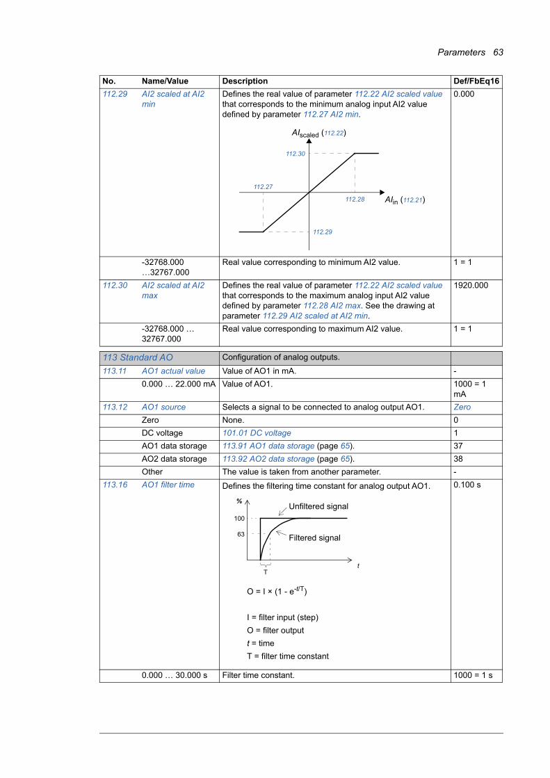
Parameters 63
112.29 AI2 scaled at AI2 min
Defines the real value of parameter 112.22 AI2 scaled value that corresponds to the minimum analog input AI2 value defined by parameter 112.27 AI2 min.
0.000
-32768.000 …32767.000
Real value corresponding to minimum AI2 value. 1 = 1
112.30 AI2 scaled at AI2 max
Defines the real value of parameter 112.22 AI2 scaled value that corresponds to the maximum analog input AI2 value defined by parameter 112.28 AI2 max. See the drawing at parameter 112.29 AI2 scaled at AI2 min.
1920.000
-32768.000 … 32767.000
Real value corresponding to maximum AI2 value. 1 = 1
113113 Standard AO Configuration of analog outputs.
113.11 AO1 actual value Value of AO1 in mA. -
0.000 … 22.000 mA Value of AO1. 1000 = 1 mA
113.12 AO1 source Selects a signal to be connected to analog output AO1. Zero
Zero None. 0
DC voltage 101.01 DC voltage 1
AO1 data storage 113.91 AO1 data storage (page 65). 37
AO2 data storage 113.92 AO2 data storage (page 65). 38
Other The value is taken from another parameter. -
113.16 AO1 filter time Defines the filtering time constant for analog output AO1. 0.100 s
0.000 … 30.000 s Filter time constant. 1000 = 1 s
No. Name/Value Description Def/FbEq16
112.30
112.28
112.27
112.29
AIin (112.21)
AIscaled (112.22)
63
%
100
Tt
O = I × (1 - e-t/T)
I = filter input (step)
O = filter output
t = time
T = filter time constant
Unfiltered signal
Filtered signal

64 Parameters
113.17 AO1 source min Defines the real value of the signal (selected by parameter 113.12 AO1 source) that corresponds to the minimum AO1 output value (defined by parameter 113.19 AO1 out at AO1 src min).
0.0
-32768.0 … 32767.0
Real signal value corresponding to minimum AO1 output value.
1 = 1
113.18 AO1 source max Defines the real value of the signal (selected by parameter 113.12 AO1 source) that corresponds to the maximum AO1 output value (defined by parameter 113.20 AO1 out at AO1 src max). See parameter 113.17 AO1 source min.
100.0
-32768.0 … 32767.0
Real signal value corresponding to maximum AO1 output value.
1 = 1
113.19 AO1 out at AO1 src min
Defines the minimum output value for analog output AO1.
See also drawing at parameter 113.17 AO1 source min.
4.000 mA
0.000 … 22.000 mA Minimum AO1 output value. 1000 = 1 mA
113.20 AO1 out at AO1 src max
Defines the maximum output value for analog output AO1.
See also drawing at parameter 113.17 AO1 source min.
20.000 mA
0.000 … 22.000 mA Maximum AO1 output value. 1000 = 1 mA
113.21 AO2 actual value Value of AO2 in mA. -
0.000 … 22.000 mA Value of AO2. 1000 = 1 mA
113.22 AO2 source Selects a signal to be connected to analog output AO2.
For the selections, see parameter 113.12 AO1 source.
Zero
113.26 AO2 filter time Defines the filtering time constant for analog output AO2. See parameter 113.16 AO1 filter time.
0.100 s
0.000 … 30.000 s Filter time constant. 1000 = 1 s
No. Name/Value Description Def/FbEq16
IAO1 (mA)
113.20
113.19
113.18 113.17
113.18113.17
113.20
113.19
Signal (real)
selected by par. 113.12
IAO1 (mA)
Signal (real)
selected by par. 113.12

Parameters 65
113.27 AO2 source min Defines the real value of the signal (selected by parameter 113.22 AO2 source) that corresponds to the minimum AO2 output value (defined by parameter 113.29 AO2 out at AO2 src min).
0.0
-32768.0 … 32767.0
Real signal value corresponding to minimum AO2 output value.
1 = 1
113.28 AO2 source max Defines the real value of the signal (selected by parameter 113.22 AO2 source) that corresponds to the maximum AO2 output value (defined by parameter 113.30 AO2 out at AO2 src max). See parameter 113.27 AO2 source min.
100.0
-32768.0 … 32767.0
Real signal value corresponding to maximum AO2 output value.
1 = 1
113.29 AO2 out at AO2 src min
Defines the minimum output value for analog output AO2.
See also drawing at parameter 113.27 AO2 source min.
4.000 mA
0.000 … 22.000 mA Minimum AO2 output value. 1000 = 1 mA
113.30 AO2 out at AO2 src max
Defines the maximum output value for analog output AO2.
See also drawing at parameter 113.27 AO2 source min.
20.000 mA
0.000 … 22.000 mA Maximum AO2 output value. 1000 = 1 mA
113.91 AO1 data storage Storage parameter for controlling analog output AO1 eg. through fieldbus.In 113.12 AO1 source, select AO1 data storage. Then set this parameter as the target of the incoming value data.
0.00
-327.68 … 327.67 Storage parameter for AO1. 100 = 1
113.92 AO2 data storage Storage parameter for controlling analog output AO2 eg. through fieldbus.In 113.22 AO2 source, select AO2 data storage. Then set this parameter as the target of the incoming value data.
0.00
-327.68 … 327.67 Storage parameter for AO2. 100 = 1
No. Name/Value Description Def/FbEq16
IAO2 (mA)
113.30
113.29
113.28 113.27
113.28113.27
113.30
113.29
Signal (real)
selected by par. 113.22
IAO2 (mA)
Signal (real)
selected by par. 113.22

66 Parameters
114114 Extension I/O module 1 Configuration of I/O extension module 1.
See also section Programmable I/O extensions (page 22).
Note: The contents of the parameter group vary according to the selected I/O extension module type.
114.01 Module 1 type Activates (and specifies the type of) I/O extension module 1. None
None Inactive. 0
FIO-01 FIO-01. 1
FIO-11 FIO-11. 2
FDIO-01 FDIO-01. 3
FAIO-01 FAIO-01. 4
114.02 Module 1 location Specifies the node number (1…3) on the control unit into which the I/O extension module is installed. (Node 1 = slot 1, node 2 = slot 2, node 3 = slot 3) Alternatively, specifies the node ID of the slot on an FEA-0x extension adapter.
Slot 1
Slot 1 Slot 1. 1
Slot 2 Slot 2. 2
Slot 3 Slot 3. 3
4…254 Node ID of the slot on the FEA-03 extension adapter. 1 = 1
114.03 Module 1 status Displays the status of I/O extension module 1. No option
No option No module detected in the specified slot. 0
No communication A module has been detected but cannot be communicated with.
1
Unknown The module type is unknown. 2
FIO-01 An FIO-01 module has been detected and is active. 3
FIO-11 An FIO-11 module has been detected and is active. 4
FAIO-01 An FAIO-01 module has been detected and is active. 24
FDIO-01 An FDIO-01 module has been detected and is active. 25
114.05 DI status (Visible when 114.01 Module 1 type = FDIO-01)Displays the status of the digital inputs on the extension module. The activation/deactivation delays (if any are specified) are ignored. A filtering time (for input mode) can be defined by parameter 114.08 DI filter time.Bit 0 indicates the status of DI1.Note: The number of active bits in this parameter depends on the number of digital input/outputs on the extension module.Example: 0101b = DI1 and DI3 are on, remainder are off.This parameter is read-only.
-
0000b…1111b Status of digital inputs. 1 = 1
114.05 DIO status (Visible when 114.01 Module 1 type = FIO-01 or FIO-11)Displays the electrical status of the digital input/outputs on the extension module. The activation/deactivation delays (if any are specified) are ignored.Bit 0 indicates the status of DIO1.Note: The number of active bits in this parameter depends on the number of digital input/outputs on the extension module.Example: 1001b = DIO1 and DIO4 are on, remainder are off.This parameter is read-only.
-
0000b…1111b Status of digital input/outputs. 1 = 1
No. Name/Value Description Def/FbEq16

Parameters 67
114.06 DI delayed status (Visible when 114.01 Module 1 type = FDIO-01)Displays the delayed status of the digital inputs on the extension module. The word is updated only after activation/deactivation delays (if any are specified).Bit 0 indicates the status of DI1.Note: The number of active bits in this parameter depends on the number of digital inputs on the extension module.Example: 0101b = DI1 and DI3 are on, remainder are off.This parameter is read-only.
-
0000b…1111b Delayed status of digital inputs. 1 = 1
114.06 DIO delayed status (Visible when 114.01 Module 1 type = FIO-01 or FIO-11)Displays the status of the digital input/outputs on the extension module. This word is updated only after activation/deactivation delays (if any are specified).Bit 0 indicates the status of DIO1.Note: The number of active bits in this parameter depends on the number of digital input/outputs on the extension module.Example: 1001b = DIO1 and DIO4 are on, remainder are off.This parameter is read-only.
-
0000b…1111b Delayed status of digital input/outputs. 1 = 1
114.08 DI filter time (Visible when 114.01 Module 1 type = FDIO-01)Defines a filtering time for parameter 114.05 DI status.
10.0 ms
0.8 … 100.0 ms Filtering time for 114.05. 10 = 1 ms
114.08 DIO filter time (Visible when 114.01 Module 1 type = FIO-01 or FIO-11)Defines a filtering time for parameter 114.05 DIO status. The filtering time will only affect the DIOs that are in input mode.
10.0 ms
0.8 … 100.0 ms Filtering time for 114.05. 10 = 1 ms
114.09 DIO1 configuration (Visible when 114.01 Module 1 type = FIO-01 or FIO-11)Selects whether DIO1 of the extension module is used as a digital input or output.
Input
Input DIO1 is used as a digital input. 0
Output DIO1 is used as a digital output. 1
114.11 DIO1 output source (Visible when 114.01 Module 1 type = FIO-01 or FIO-11)Selects a signal to be connected to digital input/output DIO1 when parameter 114.09 DIO1 configuration is set to Output.
Not energized
Not energized Output is not energized. 0
Energized Output is energized. 1
Ready Bit 0 of 106.11 Main status word (see page 48). Output is energized when the supply unit is ready.
2
Charge ready Bit 1 of 106.11 Main status word (see page 48). Output is energized when the intermediate circuit DC charging is ready.
3
Enabled Bit 0 of 106.16 Drive status word 1 (see page 48). Output is energized when the supply unit is enabled.
4
Started Bit 5 of 106.16 Drive status word 1 (see page 48). Output is energized when the supply unit is started.
5
Running Bit 4 of 106.16 Drive status word 1 (see page 48). Output is energized when the supply unit is running.
6
Warning Bit 7 of 106.11 Main status word (see page 48). Output is energized when a warning is active.
13
Fault Bit 3 of 106.11 Main status word (see page 48). Output is energized when a fault is active.
14
MCB Bit 13 of 106.16 Drive status word 1 (see page 48). Output is energized when MCB closing command is given.
15
No. Name/Value Description Def/FbEq16

68 Parameters
Charging Bit 12 of 106.16 Drive status word 1 (see page 48). Output is energized when the external charging has charged the supply unit.
16
Other A specific bit in another parameter. -
114.12 DI1 ON delay (Visible when 114.01 Module 1 type = FDIO-01)Defines the activation delay for digital input DI1.
0.00 s
tOn = 114.12 DI1 ON delaytOff = 114.13 DI1 OFF delay*Electrical status of DI or status of selected source (in output mode). Indicated by 114.05 DI status.**Indicated by 114.06 DI delayed status.
0.00 … 3000.00 s Activation delay for DI1. 10 = 1 s
114.12 DIO1 ON delay (Visible when 114.01 Module 1 type = FIO-01 or FIO-11)Defines the activation delay for digital input/output DIO1.
0.0 s
tOn = 114.12 DIO1 ON delaytOff = 114.13 DIO1 OFF delay*Electrical status of DIO (in input mode) or status of selected source (in output mode). Indicated by 114.05 DIO status.**Indicated by 114.06 DIO delayed status.
0.0 … 3000.0 s Activation delay for DIO1. 10 = 1 s
114.13 DI1 OFF delay (Visible when 114.01 Module 1 type = FDIO-01)Defines the deactivation delay for digital input DI1. See parameter 114.12 DI1 ON delay.
0.00 s
0.00 … 3000.00 s Deactivation delay for DI1. 10 = 1 s
114.13 DIO1 OFF delay (Visible when 114.01 Module 1 type = FIO-01 or FIO-11)Defines the deactivation delay for digital input/output DIO1. See parameter 114.12 DIO1 ON delay.
0.0 s
0.0 … 3000.0 s Deactivation delay for DIO1. 10 = 1 s
114.14 DIO2 configuration (Visible when 114.01 Module 1 type = FIO-01 or FIO-11)Selects whether DIO2 of the extension module is used as a digital input or output.
Input
Input DIO2 is used as a digital input. 0
Output DIO2 is used as a digital output. 1
114.16 DIO2 output source (Visible when 114.01 Module 1 type = FIO-01 or FIO-11)Selects a signal to be connected to digital input/output DIO2 when parameter 114.14 DIO2 configuration is set to Output.For the available selections, see parameter 114.11 DIO1 output source.
Not energized
No. Name/Value Description Def/FbEq16
1
0
1
0
tOn tOff tOn tOff
*DI status
**Delayed DI status
Time
1
0
1
0
tOn tOff tOn tOff
*DIO status
**Delayed DIO status
Time

Parameters 69
114.17 DI2 ON delay (Visible when 114.01 Module 1 type = FDIO-01)Defines the activation delay for digital input DI2. See parameter 114.12 DI1 ON delay.
0.00 s
0.00 … 3000.00 s Activation delay for DI2. 10 = 1 s
114.17 DIO2 ON delay (Visible when 114.01 Module 1 type = FIO-01 or FIO-11)Defines the activation delay for digital input/output DIO2.
0.0 s
tOn = 114.17 DIO2 ON delaytOff = 114.18 DIO2 OFF delay*Electrical status of DIO (in input mode) or status of selected source (in output mode). Indicated by 114.05 DIO status.**Indicated by 114.06 DIO delayed status.
0.0 … 3000.0 s Activation delay for DIO2. 10 = 1 s
114.18 DI2 OFF delay (Visible when 114.01 Module 1 type = FDIO-01)Defines the deactivation delay for digital input DI2. See parameter 114.12 DI1 ON delay.
0.00 s
0.00 … 3000.00 s Deactivation delay for DI2. 10 = 1 s
114.18 DIO2 OFF delay (Visible when 114.01 Module 1 type = FIO-01 or FIO-11)Defines the deactivation delay for digital input/output DIO2. See parameter 114.17 DIO2 ON delay.
0.0 s
0.0 … 3000.0 s Deactivation delay for DIO2. 10 = 1 s
114.19 DIO3 configuration (Visible when 114.01 Module 1 type = FIO-01)Selects whether DIO3 of the extension module is used as a digital input or output.
Input
Input DIO3 is used as a digital input. 0
Output DIO3 is used as a digital output. 1
114.19 AI supervision function
(Visible when 114.01 Module 1 type = FIO-11 or FAIO-01)Selects how the supply unit reacts when an analog input signal moves out of the minimum and/or maximum limits specified for the input.The inputs and the limits to be observed are selected by parameter 114.20 AI supervision selection.
No action
No action No action taken. 0
Fault Supply unit trips on 8E06 AI supervision. 1
Warning Supply unit generates an AE67 AI supervision warning. 2
No. Name/Value Description Def/FbEq16
1
0
1
0
tOn tOff tOn tOff
*DIO status
**Delayed DIO status
Time

70 Parameters
114.20 AI supervision selection
(Visible when 114.01 Module 1 type = FIO-11 or FAIO-01)Specifies the analog input limits to be supervised. See parameter 114.19 AI supervision function.
0000h
0000h…FFFFh Activation of analog input supervision. 1 = 1
114.21 DIO3 output source (Visible when 114.01 Module 1 type = FIO-01)Selects a signal to be connected to digital input/output DIO3 when parameter 114.19 DIO3 configuration is set to Output.For the available selections, see parameter 114.11 DIO1 output source.
Not energized
114.22 DI3 ON delay (Visible when 114.01 Module 1 type = FDIO-01)Defines the activation delay for digital input DI3. See parameter 114.12 DI1 ON delay.
0.00 s
0.00 … 3000.00 s Activation delay for DI3. 10 = 1 s
114.22 DIO3 ON delay (Visible when 114.01 Module 1 type = FIO-01)Defines the activation delay for digital input/output DIO3.
0.0 s
tOn = 114.22 DIO3 ON delaytOff = 114.23 DIO3 OFF delay*Electrical status of DIO (in input mode) or status of selected source (in output mode). Indicated by 114.05 DIO status.**Indicated by 114.06 DIO delayed status.
0.0 … 3000.0 s Activation delay for DIO3. 10 = 1 s
114.22 AI force sel (Visible when 114.01 Module 1 type = FIO-11 or FAIO-01)The true readings of the analog inputs can be overridden for eg. testing purposes. A forced value parameter is provided for each analog input, and its value is applied whenever the corresponding bit in this parameter is 1.
00000000h
00000000h … FFFFFFFFh
Forced values selector for analog inputs. 1 = 1
No. Name/Value Description Def/FbEq16
Bit Name Description0 AI1 < MIN 1 = Minimum limit supervision of AI1 active.1 AI1 > MAX 1 = Maximum limit supervision of AI1 active.2 AI2 < MIN 1 = Minimum limit supervision of AI2 active.3 AI2 > MAX 1 = Maximum limit supervision of AI2 active.4 AI3 < MIN 1 = Minimum limit supervision of AI3 active.5 AI3 > MAX 1 = Maximum limit supervision of AI3 active.6…15 Reserved
1
0
1
0
tOn tOff tOn tOff
*DIO status
**Delayed DIO status
Time
Bit Value0 1 = Force AI1 to value of parameter 114.28 AI1 force data.1 1 = Force AI2 to value of parameter 114.43 AI2 force data.2 1 = Force AI3 to value of parameter 114.58 AI3 force data.3…31 Reserved.

Parameters 71
114.23 DI3 OFF delay (Visible when 114.01 Module 1 type = FDIO-01)Defines the deactivation delay for digital input DI3. See parameter 114.12 DI1 ON delay.
0.00 s
0.00 … 3000.00 s Deactivation delay for DI3. 10 = 1 s
114.23 DIO3 OFF delay (Visible when 114.01 Module 1 type = FIO-01)Defines the deactivation delay for digital input/output DIO3. See parameter 114.22 DIO3 ON delay.
0.0 s
0.0 … 3000.0 s Deactivation delay for DIO3. 10 = 1 s
114.24 DIO4 configuration (Visible when 114.01 Module 1 type = FIO-01)Selects whether DIO4 of the I/O extension module is used as a digital input or output.
Input
Input DIO4 is used as a digital input. 0
Output DIO4 is used as a digital output. 1
114.26 DIO4 output source (Visible when 114.01 Module 1 type = FIO-01)Selects a signal to be connected to digital input/output DIO4 when parameter 114.24 DIO4 configuration is set to Output.For the available selections, see parameter 114.11 DIO1 output source.
Not energized
114.26 AI1 actual value (Visible when 114.01 Module 1 type = FIO-11 or FAIO-01)Displays the value of analog input AI1 in mA or V (depending on whether the input is set to current or voltage).This parameter is read-only.
-
-22.000 … 22.000 mA or V
Value of analog input AI1. 1000 = 1 mA or V
114.27 DIO4 ON delay (Visible when 114.01 Module 1 type = FIO-01)Defines the activation delay for digital input/output DIO4.
0.0 s
tOn = 114.27 DIO4 ON delaytOff = 114.28 DIO4 OFF delay*Electrical status of DIO (in input mode) or status of selected source (in output mode). Indicated by 114.05 DIO status.**Indicated by 114.06 DIO delayed status.
0.0 … 3000.0 s Activation delay for DIO4. 10 = 1 s
114.27 AI1 scaled value (Visible when 114.01 Module 1 type = FIO-11 or FAIO-01)Displays the value of analog input AI1 after scaling. See parameter 114.35 AI1 scaled at AI1 min.This parameter is read-only.
-
-32768.000 … 32767.000
Scaled value of analog input AI1. 1 = 1
114.28 DIO4 OFF delay (Visible when 114.01 Module 1 type = FIO-01)Defines the deactivation delay for digital input/output DIO4. See parameter 114.27 DIO4 ON delay.
0.0 s
0.0 … 3000.0 s Deactivation delay for DIO4. 10 = 1 s
114.28 AI1 force data (Visible when 114.01 Module 1 type = FIO-11 or FAIO-01)Forced value that can be used instead of the true reading of the input. See parameter 114.22 AI force sel.
-
-22.000 … 22.000 mA or V
Forced value of analog input AI1. 1000 = 1 mA or V
No. Name/Value Description Def/FbEq16
1
0
1
0
tOn tOff tOn tOff
*DIO status
**Delayed DIO status
Time

72 Parameters
114.29 AI1 HW switch pos (Visible when 114.01 Module 1 type = FIO-11 or FAIO-01)Shows the position of the hardware current/voltage selector on the I/O extension module.Note: The setting of the current/voltage selector must match the unit selection made in parameter 114.30 AI1 unit selection.
-
V Volts. 2
mA Milliamperes. 10
114.30 AI1 unit selection (Visible when 114.01 Module 1 type = FIO-11 or FAIO-01)Selects the unit for readings and settings related to analog input AI1.Note: This setting must match the corresponding hardware setting on the I/O extension module (see the manual of the I/O extension module). The hardware setting is shown by parameter 114.29 AI1 HW switch pos.
mA
V Volts. 2
mA Milliamperes. 10
114.31 RO status (Visible when 114.01 Module 1 type = FIO-01 or FDIO-01)Status of relay outputs on the I/O extension module. Example: 00000001b = RO1 is energized, RO2 is de-energized.
-
0000h…FFFFh Status of relay outputs. 1 = 1
114.31 AI1 filter gain (Visible when 114.01 Module 1 type = FIO-11 or FAIO-01)Selects a hardware filtering time for AI1.See also parameter 114.32 AI1 filter time.
No filtering
No filtering No filtering. 0
125 us 125 microseconds. 1
250 us 250 microseconds. 2
500 us 500 microseconds. 3
1 ms 1 millisecond. 4
2 ms 2 milliseconds. 5
4 ms 4 milliseconds. 6
7.9375 ms 7.9375 milliseconds. 7
114.32 AI1 filter time (Visible when 114.01 Module 1 type = FIO-11 or FAIO-01)Defines the filter time constant for analog input AI1.
Note: The signal is also filtered due to the signal interface hardware. See parameter 114.31 AI1 filter gain.
0.040 s
0.000 … 30.000 s Filter time constant. 1000 = 1 s
No. Name/Value Description Def/FbEq16
63
%
100
Tt
O = I × (1 - e-t/T)
I = filter input (step)O = filter outputt = timeT = filter time constant
Unfiltered signal
Filtered signal

Parameters 73
114.33 AI1 min (Visible when 114.01 Module 1 type = FIO-11 or FAIO-01)Defines the minimum value for analog input AI1.
0.000 mA or V
-22.000 … 22.000 mA or V
Minimum value of AI1. 1000 = 1 mA or V
114.34 RO1 source (Visible when 114.01 Module 1 type = FIO-01 or FDIO-01)Selects a signal to be connected to relay output RO1.For the available selections, see parameter 114.11 DIO1 output source.
Not energized
114.34 AI1 max (Visible when 114.01 Module 1 type = FIO-11 or FAIO-01)Defines the maximum value for analog input AI1.
10.000 mA or V
-22.000 … 22.000 mA or V
Maximum value of AI1. 1000 = 1 mA or V
114.35 RO1 ON delay (Visible when 114.01 Module 1 type = FIO-01 or FDIO-01)Defines the activation delay for relay output RO1.
0.0 s
tOn = 114.35 RO1 ON delaytOff = 114.36 RO1 OFF delay
0.0 … 3000.0 s Activation delay for RO1. 10 = 1 s
114.35 AI1 scaled at AI1 min
(Visible when 114.01 Module 1 type = FIO-11 or FAIO-01)Defines the real value that corresponds to the minimum analog input AI1 value defined by parameter 114.33 AI1 min.
0.000
-32768.000 … 32767.000
Real value corresponding to minimum AI1 value. 1 = 1
114.36 RO1 OFF delay (Visible when 114.01 Module 1 type = FIO-01 or FDIO-01)Defines the deactivation delay for relay output RO1. See parameter 114.35 RO1 ON delay.
0.0 s
0.0 … 3000.0 s Deactivation delay for RO1. 10 = 1 s
114.36 AI1 scaled at AI1 max
(Visible when 114.01 Module 1 type = FIO-11 or FAIO-01)Defines the real value that corresponds to the maximum analog input AI1 value defined by parameter 114.34 AI1 max. See the drawing at parameter 114.35 AI1 scaled at AI1 min.
1500.0
-32768.000 … 32767.000
Real value corresponding to maximum AI1 value. 1 = 1
No. Name/Value Description Def/FbEq16
1
0
1
0
tOn tOff tOn tOff
Status of selectedsource
RO status
Time
114.36
114.34
114.33
114.35
AIin (114.26)
AIscaled (114.27)

74 Parameters
114.37 RO2 source (Visible when 114.01 Module 1 type = FIO-01 or FDIO-01)Selects a signal to be connected to relay output RO2.For the available selections, see parameter 114.11 DIO1 output source.
Not energized
114.38 RO2 ON delay (Visible when 114.01 Module 1 type = FIO-01 or FDIO-01)Defines the activation delay for relay output RO2.
0.0 s
tOn = 114.38 RO2 ON delaytOff = 114.39 RO2 OFF delay
0.0 … 3000.0 s Activation delay for RO2. 10 = 1 s
114.39 RO2 OFF delay (Visible when 114.01 Module 1 type = FIO-01 or FDIO-01)Defines the deactivation delay for relay output RO1. See parameter 114.35 RO1 ON delay.
0.0 s
0.0 … 3000.0 s Deactivation delay for RO2. 10 = 1 s
114.41 AI2 actual value (Visible when 114.01 Module 1 type = FIO-11 or FAIO-01)Displays the value of analog input AI2 in mA or V (depending on whether the input is set to current or voltage).This parameter is read-only.
-
-22.000 … 22.000 mA or V
Value of analog input AI2. 1000 = 1 mA or V
114.42 AI2 scaled value (Visible when 114.01 Module 1 type = FIO-11 or FAIO-01)Displays the value of analog input AI2 after scaling. See parameter 114.50 AI2 scaled at AI2 min.This parameter is read-only.
-
-32768.000 … 32767.000
Scaled value of analog input AI2. 1 = 1
114.43 AI2 force data (Visible when 114.01 Module 1 type = FIO-11 or FAIO-01)Forced value that can be used instead of the true reading of the input. See parameter 114.22 AI force sel.
0.000 mA
-22.000 … 22.000 mA or V
Forced value of analog input AI2. 1000 = 1 mA or V
114.44 AI2 HW switch pos (Visible when 114.01 Module 1 type = FIO-11 or FAIO-01)Shows the position of the hardware current/voltage selector on the I/O extension module.Note: The setting of the current/voltage selector must match the unit selection made in parameter 114.45 AI2 unit selection.
-
V Volts. 2
mA Milliamperes. 10
114.45 AI2 unit selection (Visible when 114.01 Module 1 type = FIO-11 or FAIO-01)Selects the unit for readings and settings related to analog input AI2.Note: This setting must match the corresponding hardware setting on the I/O extension module (see the manual of the I/O extension module). The hardware setting is shown by parameter 114.44 AI2 HW switch pos.
mA
V Volts. 2
mA Milliamperes. 10
No. Name/Value Description Def/FbEq16
1
0
1
0
tOn tOff tOn tOff
Status of selectedsource
RO status
Time

Parameters 75
114.46 AI2 filter gain (Visible when 114.01 Module 1 type = FIO-11 or FAIO-01)Selects a hardware filtering time for AI2.See also parameter 114.47 AI2 filter time.
No filtering
No filtering No filtering. 0
125 us 125 microseconds. 1
250 us 250 microseconds. 2
500 us 500 microseconds. 3
1 ms 1 millisecond. 4
2 ms 2 milliseconds. 5
4 ms 4 milliseconds. 6
7.9375 ms 7.9375 milliseconds. 7
114.47 AI2 filter time (Visible when 114.01 Module 1 type = FIO-11 or FAIO-01)Defines the filter time constant for analog input AI2.
Note: The signal is also filtered due to the signal interface hardware. See parameter 114.46 AI2 filter gain.
0.100 s
0.000 … 30.000 s Filter time constant. 1000 = 1 s
114.48 AI2 min (Visible when 114.01 Module 1 type = FIO-11 or FAIO-01)Defines the minimum value for analog input AI2.
0.000 mA or V
-22.000 … 22.000 mA or V
Minimum value of AI2. 1000 = 1 mA or V
114.49 AI2 max (Visible when 114.01 Module 1 type = FIO-11 or FAIO-01)Defines the maximum value for analog input AI2.
10.000 mA or V
-22.000 … 22.000 mA or V
Maximum value of AI2. 1000 = 1 mA or V
No. Name/Value Description Def/FbEq16
63
%
100
Tt
O = I × (1 - e-t/T)
I = filter input (step)O = filter outputt = timeT = filter time constant
Unfiltered signal
Filtered signal

76 Parameters
114.50 AI2 scaled at AI2 min
(Visible when 114.01 Module 1 type = FIO-11 or FAIO-01)Defines the real value that corresponds to the minimum analog input AI2 value defined by parameter 114.48 AI2 min.
0.000
-32768.000 … 32767.000
Real value corresponding to minimum AI2 value. 1 = 1
114.51 AI2 scaled at AI2 max
(Visible when 114.01 Module 1 type = FIO-11 or FAIO-01)Defines the real value that corresponds to the maximum analog input AI2 value defined by parameter 114.49 AI2 max. See the drawing at parameter 114.50 AI2 scaled at AI2 min.
1500.0
-32768.000 … 32767.000
Real value corresponding to maximum AI2 value. 1 = 1
114.56 AI3 actual value (Visible when 114.01 Module 1 type = FIO-11)Displays the value of analog input AI3 in mA or V (depending on whether the input is set to current or voltage).This parameter is read-only.
-
-22.000 … 22.000 mA or V
Value of analog input AI3. 1000 = 1 mA or V
114.57 AI3 scaled value (Visible when 114.01 Module 1 type = FIO-11)Displays the value of analog input AI3 after scaling. See parameter 114.65 AI3 scaled at AI3 min.This parameter is read-only.
-
-32768.000 … 32767.000
Scaled value of analog input AI3. 1 = 1
114.58 AI3 force data (Visible when 114.01 Module 1 type = FIO-11)Forced value that can be used instead of the true reading of the input. See parameter 114.22 AI force sel.
0.000 mA
-22.000 … 22.000 mA or V
Forced value of analog input AI3. 1000 = 1 mA or V
114.59 AI3 HW switch pos (Visible when 114.01 Module 1 type = FIO-11)Shows the position of the hardware current/voltage selector on the I/O extension module.Note: The setting of the current/voltage selector must match the unit selection made in parameter 114.60 AI3 unit selection.
-
V Volts. 2
mA Milliamperes. 10
No. Name/Value Description Def/FbEq16
114.51
114.49
114.48
114.50
AIin (114.41)
AIscaled (114.42)

Parameters 77
114.60 AI3 unit selection (Visible when 114.01 Module 1 type = FIO-11)Selects the unit for readings and settings related to analog input AI3.Note: This setting must match the corresponding hardware setting on the I/O extension module (see the manual of the I/O extension module). The hardware setting is shown by parameter 114.59 AI3 HW switch pos.
mA
V Volts. 2
mA Milliamperes. 10
114.61 AI3 filter gain (Visible when 114.01 Module 1 type = FIO-11)Selects a hardware filtering time for AI3.See also parameter 114.62 AI3 filter time.
No filtering
No filtering No filtering. 0
125 us 125 microseconds. 1
250 us 250 microseconds. 2
500 us 500 microseconds. 3
1 ms 1 millisecond. 4
2 ms 2 milliseconds. 5
4 ms 4 milliseconds. 6
7.9375 ms 7.9375 milliseconds. 7
114.62 AI3 filter time (Visible when 114.01 Module 1 type = FIO-11)Defines the filter time constant for analog input AI3.
Note: The signal is also filtered due to the signal interface hardware. See parameter 114.61 AI3 filter gain.
0.100 s
0.000 … 30.000 s Filter time constant. 1000 = 1 s
114.63 AI3 min (Visible when 114.01 Module 1 type = FIO-11)Defines the minimum value for analog input AI3.
0.000 mA or V
-22.000 … 22.000 mA or V
Minimum value of AI3. 1000 = 1 mA or V
114.64 AI3 max (Visible when 114.01 Module 1 type = FIO-11)Defines the maximum value for analog input AI3.
10.000 mA or V
-22.000 … 22.000 mA or V
Maximum value of AI3. 1000 = 1 mA or V
No. Name/Value Description Def/FbEq16
63
%
100
Tt
O = I × (1 - e-t/T)
I = filter input (step)O = filter outputt = timeT = filter time constant
Unfiltered signal
Filtered signal

78 Parameters
114.65 AI3 scaled at AI3 min
(Visible when 114.01 Module 1 type = FIO-11)Defines the real value that corresponds to the minimum analog input AI3 value defined by parameter 114.63 AI3 min.
0.000
-32768.000 … 32767.000
Real value corresponding to minimum AI3 value. 1 = 1
114.66 AI3 scaled at AI3 max
(Visible when 114.01 Module 1 type = FIO-11)Defines the real value that corresponds to the maximum analog input AI3 value defined by parameter 114.64 AI3 max. See the drawing at parameter 114.65 AI3 scaled at AI3 min.
1500.0
-32768.000 … 32767.000
Real value corresponding to maximum AI3 value. 1 = 1
114.71 AO force selection (Visible when 114.01 Module 1 type = FIO-11 or FAIO-01)The value of the analog output can be overridden for eg. testing purposes. A forced value parameter (114.78 AO1 force data) is provided for the analog output, and its value is applied whenever the corresponding bit in this parameter is 1.
00000000h
00000000h … FFFFFFFFh
Forced values selector for analog outputs. 1 = 1
114.76 AO1 actual value (Visible when 114.01 Module 1 type = FIO-11 or FAIO-01)Displays the value of AO1 in mA.This parameter is read-only.
-
0.000 … 22.000 mA Value of AO1. 1000 = 1 mA
114.77 AO1 source (Visible when 114.01 Module 1 type = FIO-11 or FAIO-01)Selects a signal to be connected to analog output AO1. Alternatively, sets the output to excitation mode to feed a constant current to a temperature sensor.
Zero
Zero None. 0
DC voltage 101.01 DC voltage 1
Line current 101.02 Line current 2
Other The value is taken from another parameter. -
114.78 AO1 force data (Visible when 114.01 Module 1 type = FIO-11 or FAIO-01)Forced value that can be used instead of the selected output signal. See parameter 114.71 AO force selection.
0.000 mA
0.000 … 22.000 mA Forced value of analog output AI1. 1000 = 1 mA
No. Name/Value Description Def/FbEq16
114.66
114.64
114.63
114.65
AIin (114.56)
AIscaled (114.57)
Bit Value0 1 = Force AO1 to value of parameter 114.78 AO1 force data.1…31 Reserved.
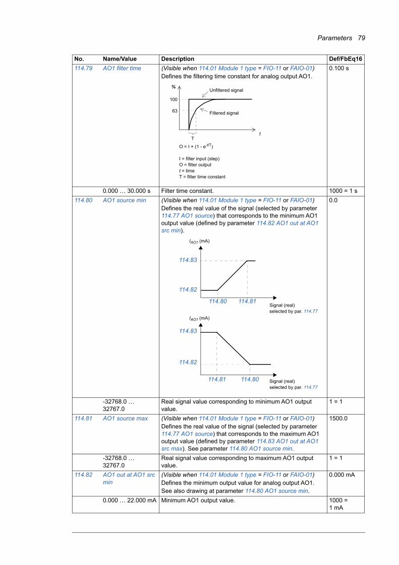
Parameters 79
114.79 AO1 filter time (Visible when 114.01 Module 1 type = FIO-11 or FAIO-01)Defines the filtering time constant for analog output AO1.
0.100 s
0.000 … 30.000 s Filter time constant. 1000 = 1 s
114.80 AO1 source min (Visible when 114.01 Module 1 type = FIO-11 or FAIO-01)Defines the real value of the signal (selected by parameter 114.77 AO1 source) that corresponds to the minimum AO1 output value (defined by parameter 114.82 AO1 out at AO1 src min).
0.0
-32768.0 … 32767.0
Real signal value corresponding to minimum AO1 output value.
1 = 1
114.81 AO1 source max (Visible when 114.01 Module 1 type = FIO-11 or FAIO-01)Defines the real value of the signal (selected by parameter 114.77 AO1 source) that corresponds to the maximum AO1 output value (defined by parameter 114.83 AO1 out at AO1 src max). See parameter 114.80 AO1 source min.
1500.0
-32768.0 … 32767.0
Real signal value corresponding to maximum AO1 output value.
1 = 1
114.82 AO1 out at AO1 src min
(Visible when 114.01 Module 1 type = FIO-11 or FAIO-01)Defines the minimum output value for analog output AO1.See also drawing at parameter 114.80 AO1 source min.
0.000 mA
0.000 … 22.000 mA Minimum AO1 output value. 1000 = 1 mA
No. Name/Value Description Def/FbEq16
63
%
100
Tt
O = I × (1 - e-t/T)
I = filter input (step)O = filter outputt = timeT = filter time constant
Unfiltered signal
Filtered signal
IAO1 (mA)
114.83
114.82
114.81 114.80
114.81114.80
114.83
114.82
Signal (real)selected by par. 114.77
IAO1 (mA)
Signal (real)selected by par. 114.77

80 Parameters
114.83 AO1 out at AO1 src max
(Visible when 114.01 Module 1 type = FIO-11 or FAIO-01)Defines the maximum output value for analog output AO1.See also drawing at parameter 114.80 AO1 source min.
20.000 mA
0.000 … 22.000 mA Maximum AO1 output value. 1000 = 1 mA
114.86 AO2 actual value (Visible when 114.01 Module 1 type = FAIO-01)Displays the value of AO2 in mA.This parameter is read-only.
-
0.000 … 22.000 mA Value of AO2. 1000 = 1 mA
114.87 AO2 source (Visible when 114.01 Module 1 type = FAIO-01)Selects a signal to be connected to analog output AO2. Alternatively, sets the output to excitation mode to feed a constant current to a temperature sensor.For the selections, see parameter 114.77 AO1 source.
Zero
114.88 AO2 force data (Visible when 114.01 Module 1 type = FAIO-01)Forced value that can be used instead of the selected output signal. See parameter 114.71 AO force selection.
0.000 mA
0.000 … 22.000 mA Forced value of analog output AO2. 1000 = 1 mA
114.89 AO2 filter time (Visible when 114.01 Module 1 type = FAIO-01)Defines the filtering time constant for analog output AO2.
0.100 s
0.000 … 30.000 s Filter time constant. 1000 = 1 s
No. Name/Value Description Def/FbEq16
63
%
100
Tt
O = I × (1 - e-t/T)
I = filter input (step)O = filter outputt = timeT = filter time constant
Unfiltered signal
Filtered signal

Parameters 81
114.90 AO2 source min (Visible when 114.01 Module 1 type = FAIO-01)Defines the real value of the signal (selected by parameter 114.87 AO2 source) that corresponds to the minimum AO2 output value (defined by parameter 114.92 AO2 out at AO2 src min).
0.0
-32768.0 … 32767.0
Real signal value corresponding to minimum AO2 output value.
1 = 1
114.91 AO2 source max (Visible when 114.01 Module 1 type = FAIO-01)Defines the real value of the signal (selected by parameter 114.87 AO2 source) that corresponds to the maximum AO2 output value (defined by parameter 114.93 AO2 out at AO2 src max). See parameter 114.90 AO2 source min.
100.0
-32768.0 … 32767.0
Real signal value corresponding to maximum AO2 output value.
1 = 1
114.92 AO2 out at AO2 src min
(Visible when 114.01 Module 1 type = FAIO-01)Defines the minimum output value for analog output AO2.See also drawing at parameter 114.90 AO2 source min.
0.000 mA
0.000 … 22.000 mA Minimum AO2 output value. 1000 = 1 mA
114.93 AO2 out at AO2 src max
(Visible when 114.01 Module 1 type = FAIO-01)Defines the maximum output value for analog output AO2.See also drawing at parameter 114.90 AO2 source min.
10.000 mA
0.000 … 22.000 mA Maximum AO2 output value. 1000 = 1 mA
115115 Extension I/O module 2 Configuration of I/O extension module 2.
See also section Programmable I/O extensions (page 22).
Note: The contents of the parameter group vary according to the selected I/O extension module type.
115.01 Module 2 type See parameter 114.01 Module 1 type. None
115.02 Module 2 location See parameter 114.02 Module 1 location. Slot 1
115.03 Module 2 status See parameter 114.03 Module 1 status. No option
115.05 DI status (Visible when 115.01 Module 2 type = FDIO-01)See parameter 114.05 DI status.
-
No. Name/Value Description Def/FbEq16
IAO2 (mA)
114.91114.90
114.93
114.92
IAO2 (mA)
Signal (real)selected by par. 114.87
114.93
114.92
114.91 114.90Signal (real)selected by par. 114.87

82 Parameters
115.05 DIO status (Visible when 115.01 Module 2 type = FIO-01 or FIO-11)See parameter 114.05 DIO status.
-
115.06 DI delayed status (Visible when 115.01 Module 2 type = FDIO-01)See parameter 114.06 DI delayed status.
-
115.06 DIO delayed status (Visible when 115.01 Module 2 type = FIO-01 or FIO-11)See parameter 114.06 DIO delayed status.
-
115.08 DI filter time (Visible when 115.01 Module 2 type = FDIO-01)See parameter 114.08 DI filter time.
10.0 ms
115.08 DIO filter time (Visible when 115.01 Module 2 type = FIO-01 or FIO-11)See parameter 114.08 DIO filter time.
10.0 ms
115.09 DIO1 configuration (Visible when 115.01 Module 2 type = FIO-01 or FIO-11)See parameter 114.09 DIO1 configuration.
Input
115.11 DIO1 output source (Visible when 115.01 Module 2 type = FIO-01 or FIO-11)See parameter 114.11 DIO1 output source.
Not energized
115.12 DI1 ON delay (Visible when 115.01 Module 2 type = FDIO-01)See parameter 114.12 DI1 ON delay.
0.00 s
115.12 DIO1 ON delay (Visible when 115.01 Module 2 type = FIO-01 or FIO-11)See parameter 114.12 DIO1 ON delay.
0.0 s
115.13 DI1 OFF delay (Visible when 115.01 Module 2 type = FDIO-01)See parameter 114.13 DI1 OFF delay.
0.00 s
115.13 DIO1 OFF delay (Visible when 115.01 Module 2 type = FIO-01 or FIO-11)See parameter 114.13 DIO1 OFF delay.
0.0 s
115.14 DIO2 configuration (Visible when 115.01 Module 2 type = FIO-01 or FIO-11)See parameter 114.14 DIO2 configuration.
Input
115.16 DIO2 output source (Visible when 115.01 Module 2 type = FIO-01 or FIO-11)See parameter 114.16 DIO2 output source.
Not energized
115.17 DI2 ON delay (Visible when 115.01 Module 2 type = FDIO-01)See parameter 114.17 DI2 ON delay.
0.00 s
115.17 DIO2 ON delay (Visible when 115.01 Module 2 type = FIO-01 or FIO-11)See parameter 114.17 DIO2 ON delay.
0.0 s
115.18 DI2 OFF delay (Visible when 115.01 Module 2 type = FDIO-01)See parameter 114.18 DI2 OFF delay.
0.00 s
115.18 DIO2 OFF delay (Visible when 115.01 Module 2 type = FIO-01 or FIO-11)See parameter 114.18 DIO2 OFF delay.
0.0 s
115.19 DIO3 configuration (Visible when 115.01 Module 2 type = FIO-01)See parameter 114.19 DIO3 configuration.
Input
115.19 AI supervision function
(Visible when 115.01 Module 2 type = FIO-11 or FAIO-01)See parameter 114.19 AI supervision function.
No action
115.20 AI supervision selection
(Visible when 115.01 Module 2 type = FIO-11 or FAIO-01)See parameter 114.20 AI supervision selection.
0000h
115.21 DIO3 output source (Visible when 115.01 Module 2 type = FIO-01)See parameter 114.21 DIO3 output source.
Not energized
115.22 DI3 ON delay (Visible when 115.01 Module 2 type = FDIO-01)See parameter 114.22 DI3 ON delay.
0.00 s
115.22 DIO3 ON delay (Visible when 115.01 Module 2 type = FIO-01)See parameter 114.22 DIO3 ON delay.
0.0 s
115.22 AI force sel (Visible when 115.01 Module 2 type = FIO-11 or FAIO-01)See parameter 114.22 AI force sel.
00000000h
115.23 DI3 OFF delay (Visible when 115.01 Module 2 type = FDIO-01)See parameter 114.23 DI3 OFF delay.
0.00 s
115.23 DIO3 OFF delay (Visible when 115.01 Module 2 type = FIO-01)See parameter 114.23 DIO3 OFF delay.
0.0 s
No. Name/Value Description Def/FbEq16

Parameters 83
115.24 DIO4 configuration (Visible when 115.01 Module 2 type = FIO-01)See parameter 114.24 DIO4 configuration.
Input
115.26 DIO4 output source (Visible when 115.01 Module 2 type = FIO-01)See parameter 114.26 DIO4 output source.
Not energized
115.26 AI1 actual value (Visible when 115.01 Module 2 type = FIO-11 or FAIO-01)See parameter 114.26 AI1 actual value.
-
115.27 DIO4 ON delay (Visible when 115.01 Module 2 type = FIO-01)See parameter 114.27 DIO4 ON delay.
0.0 s
115.27 AI1 scaled value (Visible when 115.01 Module 2 type = FIO-11 or FAIO-01)See parameter 114.27 AI1 scaled value.
-
115.28 DIO4 OFF delay (Visible when 115.01 Module 2 type = FIO-01)See parameter 114.28 DIO4 OFF delay.
0.0 s
115.28 AI1 force data (Visible when 115.01 Module 2 type = FIO-11 or FAIO-01)See parameter 114.28 AI1 force data.
-
115.29 AI1 HW switch pos (Visible when 115.01 Module 2 type = FIO-11 or FAIO-01)See parameter 114.29 AI1 HW switch pos.
-
115.30 AI1 unit selection (Visible when 115.01 Module 2 type = FIO-11 or FAIO-01)See parameter 114.30 AI1 unit selection.
mA
115.31 RO status (Visible when 115.01 Module 2 type = FIO-01 or FDIO-01)See parameter 114.31 RO status.
-
115.31 AI1 filter gain (Visible when 115.01 Module 2 type = FIO-11 or FAIO-01)See parameter 114.31 AI1 filter gain.
No filtering
115.32 AI1 filter time (Visible when 115.01 Module 2 type = FIO-11 or FAIO-01)See parameter 114.32 AI1 filter time.
0.040 s
115.33 AI1 min (Visible when 115.01 Module 2 type = FIO-11 or FAIO-01)See parameter 114.33 AI1 min.
0.000 mA or V
115.34 RO1 source (Visible when 115.01 Module 2 type = FIO-01 or FDIO-01)See parameter 114.34 RO1 source.
Not energized
115.34 AI1 max (Visible when 115.01 Module 2 type = FIO-11 or FAIO-01)See parameter 114.34 AI1 max.
10.000 mA or V
115.35 RO1 ON delay (Visible when 115.01 Module 2 type = FIO-01 or FDIO-01)See parameter 114.35 RO1 ON delay.
0.0 s
115.35 AI1 scaled at AI1 min
(Visible when 115.01 Module 2 type = FIO-11 or FAIO-01)See parameter 114.35 AI1 scaled at AI1 min.
0.000
115.36 RO1 OFF delay (Visible when 115.01 Module 2 type = FIO-01 or FDIO-01)See parameter 114.36 RO1 OFF delay.
0.0 s
115.36 AI1 scaled at AI1 max
(Visible when 115.01 Module 2 type = FIO-11 or FAIO-01)See parameter 114.36 AI1 scaled at AI1 max.
1500.0
115.37 RO2 source (Visible when 115.01 Module 2 type = FIO-01 or FDIO-01)See parameter 114.37 RO2 source.
Not energized
115.38 RO2 ON delay (Visible when 115.01 Module 2 type = FIO-01 or FDIO-01)See parameter 114.38 RO2 ON delay.
0.0 s
115.39 RO2 OFF delay (Visible when 115.01 Module 2 type = FIO-01 or FDIO-01)See parameter 114.39 RO2 OFF delay.
0.0 s
115.41 AI2 actual value (Visible when 115.01 Module 2 type = FIO-11 or FAIO-01)See parameter 114.41 AI2 actual value.
-
115.42 AI2 scaled value (Visible when 115.01 Module 2 type = FIO-11 or FAIO-01)See parameter 114.42 AI2 scaled value.
-
115.43 AI2 force data (Visible when 115.01 Module 2 type = FIO-11 or FAIO-01)See parameter 114.43 AI2 force data.
0.000 mA
115.44 AI2 HW switch pos (Visible when 115.01 Module 2 type = FIO-11 or FAIO-01)See parameter 114.44 AI2 HW switch pos.
-
No. Name/Value Description Def/FbEq16

84 Parameters
115.45 AI2 unit selection (Visible when 115.01 Module 2 type = FIO-11 or FAIO-01)See parameter 114.45 AI2 unit selection.
mA
115.46 AI2 filter gain (Visible when 115.01 Module 2 type = FIO-11 or FAIO-01)See parameter 114.46 AI2 filter gain.
No filtering
115.47 AI2 filter time (Visible when 115.01 Module 2 type = FIO-11 or FAIO-01)See parameter 114.47 AI2 filter time.
0.100 s
115.48 AI2 min (Visible when 115.01 Module 2 type = FIO-11 or FAIO-01)See parameter 114.48 AI2 min.
0.000 mA or V
115.49 AI2 max (Visible when 115.01 Module 2 type = FIO-11 or FAIO-01)See parameter 114.49 AI2 max.
10.000 mA or V
115.50 AI2 scaled at AI2 min
(Visible when 115.01 Module 2 type = FIO-11 or FAIO-01)See parameter 114.50 AI2 scaled at AI2 min.
0.000
115.51 AI2 scaled at AI2 max
(Visible when 115.01 Module 2 type = FIO-11 or FAIO-01)See parameter 114.51 AI2 scaled at AI2 max.
1500.0
115.56 AI3 actual value (Visible when 115.01 Module 2 type = FIO-11)See parameter 114.56 AI3 actual value.
-
115.57 AI3 scaled value (Visible when 115.01 Module 2 type = FIO-11)See parameter 114.57 AI3 scaled value.
-
115.58 AI3 force data (Visible when 115.01 Module 2 type = FIO-11)See parameter 114.58 AI3 force data.
0.000 mA
115.59 AI3 HW switch pos (Visible when 115.01 Module 2 type = FIO-11)See parameter 114.59 AI3 HW switch pos.
-
115.60 AI3 unit selection (Visible when 115.01 Module 2 type = FIO-11)See parameter 114.60 AI3 unit selection.
mA
115.61 AI3 filter gain (Visible when 115.01 Module 2 type = FIO-11)See parameter 114.61 AI3 filter gain.
No filtering
115.62 AI3 filter time (Visible when 115.01 Module 2 type = FIO-11)See parameter 114.62 AI3 filter time.
0.100 s
115.63 AI3 min (Visible when 115.01 Module 2 type = FIO-11)See parameter 114.63 AI3 min.
0.000 mA or V
115.64 AI3 max (Visible when 115.01 Module 2 type = FIO-11)See parameter 114.64 AI3 max.
10.000 mA or V
115.65 AI3 scaled at AI3 min
(Visible when 115.01 Module 2 type = FIO-11)See parameter 114.65 AI3 scaled at AI3 min.
0.000
115.66 AI3 scaled at AI3 max
(Visible when 115.01 Module 2 type = FIO-11)See parameter 114.66 AI3 scaled at AI3 max.
1500.0
115.71 AO force selection (Visible when 115.01 Module 2 type = FIO-11 or FAIO-01)See parameter 114.71 AO force selection.
00000000h
115.76 AO1 actual value (Visible when 115.01 Module 2 type = FIO-11 or FAIO-01)See parameter 114.76 AO1 actual value.
-
115.77 AO1 source (Visible when 115.01 Module 2 type = FIO-11 or FAIO-01)See parameter 114.77 AO1 source.
Zero
115.78 AO1 force data (Visible when 115.01 Module 2 type = FIO-11 or FAIO-01)See parameter 114.78 AO1 force data.
0.000 mA
115.79 AO1 filter time (Visible when 115.01 Module 2 type = FIO-11 or FAIO-01)See parameter 114.79 AO1 filter time.
0.100 s
115.80 AO1 source min (Visible when 115.01 Module 2 type = FIO-11 or FAIO-01)See parameter 114.80 AO1 source min.
0.0
115.81 AO1 source max (Visible when 115.01 Module 2 type = FIO-11 or FAIO-01)See parameter 114.81 AO1 source max.
1500.0
115.82 AO1 out at AO1 src min
(Visible when 115.01 Module 2 type = FIO-11 or FAIO-01)See parameter 114.82 AO1 out at AO1 src min.
0.000 mA
No. Name/Value Description Def/FbEq16

Parameters 85
115.83 AO1 out at AO1 src max
(Visible when 115.01 Module 2 type = FIO-11 or FAIO-01)See parameter 114.83 AO1 out at AO1 src max.
20.000 mA
115.86 AO2 actual value (Visible when 115.01 Module 2 type = FAIO-01)See parameter 114.86 AO2 actual value.
-
115.87 AO2 source (Visible when 115.01 Module 2 type = FAIO-01)See parameter 114.87 AO2 source.
Zero
115.88 AO2 force data (Visible when 115.01 Module 2 type = FAIO-01)See parameter 114.88 AO2 force data.
0.000 mA
115.89 AO2 filter time (Visible when 115.01 Module 2 type = FAIO-01)See parameter 114.89 AO2 filter time.
0.100 s
115.90 AO2 source min (Visible when 115.01 Module 2 type = FAIO-01)See parameter 114.90 AO2 source min.
0.0
115.91 AO2 source max (Visible when 115.01 Module 2 type = FAIO-01)See parameter 114.91 AO2 source max.
100.0
115.92 AO2 out at AO2 src min
(Visible when 115.01 Module 2 type = FAIO-01)See parameter 114.92 AO2 out at AO2 src min.
0.000 mA
115.93 AO2 out at AO2 src max
(Visible when 115.01 Module 2 type = FAIO-01)See parameter 114.93 AO2 out at AO2 src max.
10.000 mA
116116 Extension I/O module 3 Configuration of I/O extension module 3.
See also section Programmable I/O extensions (page 22).
Note: The contents of the parameter group vary according to the selected I/O extension module type.
116.01 Module 3 type See parameter 114.01 Module 1 type. None
116.02 Module 3 location See parameter 114.02 Module 1 location. Slot 1
116.03 Module 3 status See parameter 114.03 Module 1 status. No option
116.05 DI status (Visible when 116.01 Module 3 type = FDIO-01)See parameter 114.05 DI status.
-
116.05 DIO status (Visible when 116.01 Module 3 type = FIO-01 or FIO-11)See parameter 114.05 DIO status.
-
116.06 DI delayed status (Visible when 116.01 Module 3 type = FDIO-01)See parameter 114.06 DI delayed status.
-
116.06 DIO delayed status (Visible when 116.01 Module 3 type = FIO-01 or FIO-11)See parameter 114.06 DIO delayed status.
-
116.08 DI filter time (Visible when 116.01 Module 3 type = FDIO-01)See parameter 114.08 DI filter time.
10.0 ms
116.08 DIO filter time (Visible when 116.01 Module 3 type = FIO-01 or FIO-11)See parameter 114.08 DIO filter time.
10.0 ms
116.09 DIO1 configuration (Visible when 116.01 Module 3 type = FIO-01 or FIO-11)See parameter 114.09 DIO1 configuration.
Input
116.11 DIO1 output source (Visible when 116.01 Module 3 type = FIO-01 or FIO-11)See parameter 114.11 DIO1 output source.
Not energized
116.12 DI1 ON delay (Visible when 116.01 Module 3 type = FDIO-01)See parameter 114.12 DI1 ON delay.
0.00 s
116.12 DIO1 ON delay (Visible when 116.01 Module 3 type = FIO-01 or FIO-11)See parameter 114.12 DIO1 ON delay.
0.0 s
116.13 DI1 OFF delay (Visible when 116.01 Module 3 type = FDIO-01)See parameter 114.13 DI1 OFF delay.
0.00 s
116.13 DIO1 OFF delay (Visible when 116.01 Module 3 type = FIO-01 or FIO-11)See parameter 114.13 DIO1 OFF delay.
0.0 s
116.14 DIO2 configuration (Visible when 116.01 Module 3 type = FIO-01 or FIO-11)See parameter 114.14 DIO2 configuration.
Input
No. Name/Value Description Def/FbEq16

86 Parameters
116.16 DIO2 output source (Visible when 116.01 Module 3 type = FIO-01 or FIO-11)See parameter 114.16 DIO2 output source.
Not energized
116.17 DI2 ON delay (Visible when 116.01 Module 3 type = FDIO-01)See parameter 114.17 DI2 ON delay.
0.00 s
116.17 DIO2 ON delay (Visible when 116.01 Module 3 type = FIO-01 or FIO-11)See parameter 114.17 DIO2 ON delay.
0.0 s
116.18 DI2 OFF delay (Visible when 116.01 Module 3 type = FDIO-01)See parameter 114.18 DI2 OFF delay.
0.00 s
116.18 DIO2 OFF delay (Visible when 116.01 Module 3 type = FIO-01 or FIO-11)See parameter 114.18 DIO2 OFF delay.
0.0 s
116.19 DIO3 configuration (Visible when 116.01 Module 3 type = FIO-01)See parameter 114.19 DIO3 configuration.
Input
116.19 AI supervision function
(Visible when 116.01 Module 3 type = FIO-11 or FAIO-01)See parameter 114.19 AI supervision function.
No action
116.20 AI supervision selection
(Visible when 116.01 Module 3 type = FIO-11 or FAIO-01)See parameter 114.20 AI supervision selection.
0000h
116.21 DIO3 output source (Visible when 116.01 Module 3 type = FIO-01)See parameter 114.21 DIO3 output source.
Not energized
116.22 DI3 ON delay (Visible when 116.01 Module 3 type = FDIO-01)See parameter 114.22 DI3 ON delay.
0.00 s
116.22 DIO3 ON delay (Visible when 116.01 Module 3 type = FIO-01)See parameter 114.22 DIO3 ON delay.
0.0 s
116.22 AI force sel (Visible when 116.01 Module 3 type = FIO-11 or FAIO-01)See parameter 114.22 AI force sel.
00000000h
116.23 DI3 OFF delay (Visible when 116.01 Module 3 type = FDIO-01)See parameter 114.23 DI3 OFF delay.
0.00 s
116.23 DIO3 OFF delay (Visible when 116.01 Module 3 type = FIO-01)See parameter 114.23 DIO3 OFF delay.
0.0 s
116.24 DIO4 configuration (Visible when 116.01 Module 3 type = FIO-01)See parameter 114.24 DIO4 configuration.
Input
116.26 DIO4 output source (Visible when 116.01 Module 3 type = FIO-01)See parameter 114.26 DIO4 output source.
Not energized
116.26 AI1 actual value (Visible when 116.01 Module 3 type = FIO-11 or FAIO-01)See parameter 114.26 AI1 actual value.
-
116.27 DIO4 ON delay (Visible when 116.01 Module 3 type = FIO-01)See parameter 114.27 DIO4 ON delay.
0.0 s
116.27 AI1 scaled value (Visible when 116.01 Module 3 type = FIO-11 or FAIO-01)See parameter 114.27 AI1 scaled value.
-
116.28 DIO4 OFF delay (Visible when 116.01 Module 3 type = FIO-01)See parameter 114.28 DIO4 OFF delay.
0.0 s
116.28 AI1 force data (Visible when 116.01 Module 3 type = FIO-11 or FAIO-01)See parameter 114.28 AI1 force data.
-
116.29 AI1 HW switch pos (Visible when 116.01 Module 3 type = FIO-11 or FAIO-01)See parameter 114.29 AI1 HW switch pos.
-
116.30 AI1 unit selection (Visible when 116.01 Module 3 type = FIO-11 or FAIO-01)See parameter 114.30 AI1 unit selection.
mA
116.31 RO status (Visible when 116.01 Module 3 type = FIO-01 or FDIO-01)See parameter 114.31 RO status.
-
116.31 AI1 filter gain (Visible when 116.01 Module 3 type = FIO-11 or FAIO-01)See parameter 114.31 AI1 filter gain.
No filtering
116.32 AI1 filter time (Visible when 116.01 Module 3 type = FIO-11 or FAIO-01)See parameter 114.32 AI1 filter time.
0.040 s
No. Name/Value Description Def/FbEq16

Parameters 87
116.33 AI1 min (Visible when 116.01 Module 3 type = FIO-11 or FAIO-01)See parameter 114.33 AI1 min.
0.000 mA or V
116.34 RO1 source (Visible when 116.01 Module 3 type = FIO-01 or FDIO-01)See parameter 114.34 RO1 source.
Not energized
116.34 AI1 max (Visible when 116.01 Module 3 type = FIO-11 or FAIO-01)See parameter 114.34 AI1 max.
10.000 mA or V
116.35 RO1 ON delay (Visible when 116.01 Module 3 type = FIO-01 or FDIO-01)See parameter 114.35 RO1 ON delay.
0.0 s
116.35 AI1 scaled at AI1 min
(Visible when 116.01 Module 3 type = FIO-11 or FAIO-01)See parameter 114.35 AI1 scaled at AI1 min.
0.000
116.36 RO1 OFF delay (Visible when 116.01 Module 3 type = FIO-01 or FDIO-01)See parameter 114.36 RO1 OFF delay.
0.0 s
116.36 AI1 scaled at AI1 max
(Visible when 116.01 Module 3 type = FIO-11 or FAIO-01)See parameter 114.36 AI1 scaled at AI1 max.
1500.0
116.37 RO2 source (Visible when 116.01 Module 3 type = FIO-01 or FDIO-01)See parameter 114.37 RO2 source.
Not energized
116.38 RO2 ON delay (Visible when 116.01 Module 3 type = FIO-01 or FDIO-01)See parameter 114.38 RO2 ON delay.
0.0 s
116.39 RO2 OFF delay (Visible when 116.01 Module 3 type = FIO-01 or FDIO-01)See parameter 114.39 RO2 OFF delay.
0.0 s
116.41 AI2 actual value (Visible when 116.01 Module 3 type = FIO-11 or FAIO-01)See parameter 114.41 AI2 actual value.
-
116.42 AI2 scaled value (Visible when 116.01 Module 3 type = FIO-11 or FAIO-01)See parameter 114.42 AI2 scaled value.
-
116.43 AI2 force data (Visible when 116.01 Module 3 type = FIO-11 or FAIO-01)See parameter 114.43 AI2 force data.
0.000 mA
116.44 AI2 HW switch pos (Visible when 116.01 Module 3 type = FIO-11 or FAIO-01)See parameter 114.44 AI2 HW switch pos.
-
116.45 AI2 unit selection (Visible when 116.01 Module 3 type = FIO-11 or FAIO-01)See parameter 114.45 AI2 unit selection.
mA
116.46 AI2 filter gain (Visible when 116.01 Module 3 type = FIO-11 or FAIO-01)See parameter 114.46 AI2 filter gain.
No filtering
116.47 AI2 filter time (Visible when 116.01 Module 3 type = FIO-11 or FAIO-01)See parameter 114.47 AI2 filter time.
0.100 s
116.48 AI2 min (Visible when 116.01 Module 3 type = FIO-11 or FAIO-01)See parameter 114.48 AI2 min.
0.000 mA or V
116.49 AI2 max (Visible when 116.01 Module 3 type = FIO-11 or FAIO-01)See parameter 114.49 AI2 max.
10.000 mA or V
116.50 AI2 scaled at AI2 min
(Visible when 116.01 Module 3 type = FIO-11 or FAIO-01)See parameter 114.50 AI2 scaled at AI2 min.
0.000
116.51 AI2 scaled at AI2 max
(Visible when 116.01 Module 3 type = FIO-11 or FAIO-01)See parameter 114.51 AI2 scaled at AI2 max.
1500.0
116.56 AI3 actual value (Visible when 116.01 Module 3 type = FIO-11)See parameter 114.56 AI3 actual value.
-
116.57 AI3 scaled value (Visible when 116.01 Module 3 type = FIO-11)See parameter 114.57 AI3 scaled value.
-
116.58 AI3 force data (Visible when 116.01 Module 3 type = FIO-11)See parameter 114.58 AI3 force data.
0.000 mA
116.59 AI3 HW switch pos (Visible when 116.01 Module 3 type = FIO-11)See parameter 114.59 AI3 HW switch pos.
-
116.60 AI3 unit selection (Visible when 116.01 Module 3 type = FIO-11)See parameter 114.60 AI3 unit selection.
mA
No. Name/Value Description Def/FbEq16

88 Parameters
116.61 AI3 filter gain (Visible when 116.01 Module 3 type = FIO-11)See parameter 114.61 AI3 filter gain.
No filtering
116.62 AI3 filter time (Visible when 116.01 Module 3 type = FIO-11)See parameter 114.62 AI3 filter time.
0.100 s
116.63 AI3 min (Visible when 116.01 Module 3 type = FIO-11)See parameter 114.63 AI3 min.
0.000 mA or V
116.64 AI3 max (Visible when 116.01 Module 3 type = FIO-11)See parameter 114.64 AI3 max.
10.000 mA or V
116.65 AI3 scaled at AI3 min
(Visible when 116.01 Module 3 type = FIO-11)See parameter 114.65 AI3 scaled at AI3 min.
0.000
116.66 AI3 scaled at AI3 max
(Visible when 116.01 Module 3 type = FIO-11)See parameter 114.66 AI3 scaled at AI3 max.
1500.0
116.71 AO force selection (Visible when 116.01 Module 3 type = FIO-11 or FAIO-01)See parameter 114.71 AO force selection.
00000000h
116.76 AO1 actual value (Visible when 116.01 Module 3 type = FIO-11 or FAIO-01)See parameter 114.76 AO1 actual value.
-
116.77 AO1 source (Visible when 116.01 Module 3 type = FIO-11 or FAIO-01)See parameter 114.77 AO1 source.
Zero
116.78 AO1 force data (Visible when 116.01 Module 3 type = FIO-11 or FAIO-01)See parameter 114.78 AO1 force data.
0.000 mA
116.79 AO1 filter time (Visible when 116.01 Module 3 type = FIO-11 or FAIO-01)See parameter 114.79 AO1 filter time.
0.100 s
116.80 AO1 source min (Visible when 116.01 Module 3 type = FIO-11 or FAIO-01)See parameter 114.80 AO1 source min.
0.0
116.81 AO1 source max (Visible when 116.01 Module 3 type = FIO-11 or FAIO-01)See parameter 114.81 AO1 source max.
1500.0
116.82 AO1 out at AO1 src min
(Visible when 116.01 Module 3 type = FIO-11 or FAIO-01)See parameter 114.82 AO1 out at AO1 src min.
0.000 mA
116.83 AO1 out at AO1 src max
(Visible when 116.01 Module 3 type = FIO-11 or FAIO-01)See parameter 114.83 AO1 out at AO1 src max.
20.000 mA
116.86 AO2 actual value (Visible when 116.01 Module 3 type = FAIO-01)See parameter 114.86 AO2 actual value.
-
116.87 AO2 source (Visible when 116.01 Module 3 type = FAIO-01)See parameter 114.87 AO2 source.
Zero
116.88 AO2 force data (Visible when 116.01 Module 3 type = FAIO-01)See parameter 114.88 AO2 force data.
0.000 mA
116.89 AO2 filter time (Visible when 116.01 Module 3 type = FAIO-01)See parameter 114.89 AO2 filter time.
0.100 s
116.90 AO2 source min (Visible when 116.01 Module 3 type = FAIO-01)See parameter 114.90 AO2 source min.
0.0
116.91 AO2 source max (Visible when 116.01 Module 3 type = FAIO-01)See parameter 114.91 AO2 source max.
100.0
116.92 AO2 out at AO2 src min
(Visible when 116.01 Module 3 type = FAIO-01)See parameter 114.92 AO2 out at AO2 src min.
0.000 mA
116.93 AO2 out at AO2 src max
(Visible when 116.01 Module 3 type = FAIO-01)See parameter 114.93 AO2 out at AO2 src max.
10.000 mA
119119 Operation mode Selection of external control location sources and operating
modes.
119.11 Ext1/Ext2 sel Selects the external control location EXT1/EXT2. EXT1
EXT1 EXT1 selected. 0
EXT2 EXT2 selected. 1
No. Name/Value Description Def/FbEq16

Parameters 89
FBA A MCW bit 11 106.01 Main control word, bit 11 received through fieldbus interface A.
2
DI1 Digital input DI1 (as indicated by 110.02 DI delayed status, bit 0).
Note: DI1 is reserved for temperature fault in the control program. Do not select it for any other use.
3
DI2 Digital input DI2 (as indicated by 110.02 DI delayed status, bit 1).
4
DI3 Digital input DI3 (as indicated by 110.02 DI delayed status, bit 2).
Note: DI3 is reserved for main breaker/contactor fault in the control program. Do not select it for any other use.
5
DI4 Digital input DI4 (as indicated by 110.02 DI delayed status, bit 3).
Note: DI4 is reserved for auxiliary circuit breaker fault in the control program. Do not select it for any other use.
6
DI5 Digital input DI5 (as indicated by 110.02 DI delayed status, bit 4).
7
DI6 Digital input DI6 (as indicated by 110.02 DI delayed status bit 5).
8
DIO1 Digital input/output DIO1 (as indicated by 111.02 DIO delayed status, bit 0).
11
DIO2 Digital input/output DIO2 (as indicated by 111.02 DIO delayed status, bit 1).
12
Other [bit] Source selection (see Terms and abbreviations on page 41). -
119.17 Local ctrl disable Enables/disables (or selects a source that enables/disables) local control.
WARNING! Before disabling local control, ensure that the control panel is not needed for stopping the supply unit.
No
No Local control enabled. 0
Yes Local control disabled. 1
120120 Start/stop Start/stop and run/start enable signal source selection;
charging settings.
120.01 Ext1 commands Selects the source of start and stop commands for external control location 1 (EXT1).
Note: This parameter cannot be changed while the converter is running.
In1 Start
Not sel No start or stop command sources selected. 0
In1 Start The source of the start and stop commands is selected by parameter 120.03 Ext1 in1. The state transitions of the source bit are interpreted as follows:
1
No. Name/Value Description Def/FbEq16
State of source (120.03)
Command
0 -> 1 Start
1 -> 0 Stop

90 Parameters
In1P Start; In2 Stop The sources of the start and stop commands are selected by parameters 120.03 Ext1 in1 and 120.04 Ext1 in2. The state transitions of the source bits are interpreted as follows:
4
Keypad The start and stop commands are taken from the control panel (or PC connected to the control panel).
11
Fieldbus A The start and stop commands are taken from fieldbus adapter A.
12
DDCS controller The start and stop commands are taken from an external (DDCS) controller.
16
120.02 Ext1 start trigger Defines whether the start signal for external control location EXT1 is edge-triggered or level-triggered.
Note: In case the settings of parameters 120.01 and 120.02 are in conflict, the setting of parameter 120.01 takes preference.
Edge
Edge The start signal is edge-triggered. 0
Level The start signal is level-triggered. 1
120.03 Ext1 in1 Selects source 1 for external control location EXT1. See parameter 120.01 Ext1 commands.
DI2
Off 0. 0
On 1. 1
DI1 Digital input DI1 (as indicated by 110.02 DI delayed status, bit 0).
Note: DI1 is reserved for temperature fault in the control program. Do not select it for any other use.
2
DI2 Digital input DI2 (as indicated by 110.02 DI delayed status, bit 1).
3
DI3 Digital input DI3 (as indicated by 110.02 DI delayed status, bit 2).
Note: DI3 is reserved for main breaker/contactor fault in the control program. Do not select it for any other use.
4
DI4 Digital input DI4 (as indicated by 110.02 DI delayed status, bit 3).
Note: DI4 is reserved for auxiliary circuit breaker fault in the control program. Do not select it for any other use.
5
DI5 Digital input DI5 (as indicated by 110.02 DI delayed status, bit 4).
6
DI6 Digital input DI6 (as indicated by 110.02 DI delayed status bit 5).
7
DIO1 Digital input/output DIO1 (as indicated by 111.02 DIO delayed status, bit 0).
10
DIO2 Digital input /output DIO2 (as indicated by 111.02 DIO delayed status, bit 1).
11
Other [bit] Source selection (see Terms and abbreviations on page 41). -
120.04 Ext1 in2 Selects source 2 for external control location EXT1. See parameter 120.01 Ext1 commands.
For the available selections, see parameter 120.03 Ext1 in1.
DI2
No. Name/Value Description Def/FbEq16
State of source 1 (120.03)
State of source 2 (120.04)
Command
0 -> 1 1 Start
Any 1 -> 0 Stop
Any 0 Stop

Parameters 91
120.06 Ext2 commands Selects the source of start and stop commands for external control location 2 (EXT2).
Note: This parameter cannot be changed while the converter is running.
Not sel
Not sel No start or stop command sources selected. 0
In1 Start The source of the start and stop commands is selected by parameter 120.08 Ext2 in1. The state transitions of the source bit are interpreted as follows:
1
In1P Start; In2 Stop The sources of the start and stop commands are selected by parameters 120.08 Ext2 in1 and 120.09 Ext2 in2. The state transitions of the source bits are interpreted as follows:
4
Keypad The start and stop commands are taken from the control panel (or PC connected to the control panel).
11
Fieldbus A The start and stop commands are taken from fieldbus adapter A.
12
DDCS controller The start and stop commands are taken from an external (DDCS) controller.
16
120.07 Ext2 start trigger Defines whether the start signal for external control location EXT2 is edge-triggered or level-triggered.
Note: In case the settings of parameters 120.06 and 120.07 are in conflict, the setting of parameter 120.06 takes preference.
Edge
Edge The start signal is edge-triggered. 0
Level The start signal is level-triggered. 1
120.08 Ext2 in1 Selects source 1 for external control location EXT2. See parameter 120.06 Ext2 commands.
For the available selections, see parameter 120.03 Ext1 in1.
Off
120.09 Ext2 in2 Selects source 2 for external control location EXT2. See parameter 120.06 Ext2 commands.
For the available selections, see parameter 120.03 Ext1 in1.
Off
120.12 Run enable 1 Selects the source of the external run enable signal. If the run enable signal is switched off, the supply unit will not start, or stops if running.
1 = Run enable.
Note: This parameter cannot be changed while the converter is running.
DI2
Off 0. 0
On 1. 1
DI1 Digital input DI1 (as indicated by 110.02 DI delayed status, bit 0).
Note: DI1 is reserved for temperature fault in the control program. Do not select it for any other use.
2
No. Name/Value Description Def/FbEq16
State of source (120.08)
Command
0 -> 1 Start
1 -> 0 Stop
State of source 1 (120.08)
State of source 2 (120.09)
Command
0 -> 1 1 Start
Any 1 -> 0 Stop
Any 0 Stop

92 Parameters
DI2 Digital input DI2 (as indicated by 110.02 DI delayed status, bit 1).
3
DI3 Digital input DI3 (as indicated by 110.02 DI delayed status, bit 2).
Note: DI3 is reserved for main breaker/contactor fault in the control program. Do not select it for any other use.
4
DI4 Digital input DI4 (as indicated by 110.02 DI delayed status, bit 3).
Note: DI4 is reserved for auxiliary circuit breaker fault in the control program. Do not select it for any other use.
5
DI5 Digital input DI5 (as indicated by 110.02 DI delayed status, bit 4).
6
DI6 Digital input DI6 (as indicated by 110.02 DI delayed status bit 5).
7
DIO1 Digital input/output DIO1 (as indicated by 111.02 DIO delayed status, bit 0).
10
DIO2 Digital input/output DIO2 (as indicated by 111.02 DIO delayed status, bit 1).
11
DIIL DIIL input (110.02 DI delayed status, bit 15). 33
Other [bit] Source selection (see Terms and abbreviations on page 41). -
120.19 Enable start signal Selects the source for the start enable signal.
1 = Start enable.
With the signal switched off, the converter will not start. (Switching the signal off while the converter is running will not stop it.)
On
Off 0. 0
On 1. 1
DI1 Digital input DI1 (as indicated by 110.02 DI delayed status, bit 0).
Note: DI1 is reserved for temperature fault in the control program. Do not select it for any other use.
2
DI2 Digital input DI2 (as indicated by 110.02 DI delayed status, bit 1).
3
DI3 Digital input DI3 (as indicated by 110.02 DI delayed status, bit 2).
Note: DI3 is reserved for main breaker/contactor fault in the control program. Do not select it for any other use.
4
DI4 Digital input DI4 (as indicated by 110.02 DI delayed status, bit 3).
Note: DI4 is reserved for auxiliary circuit breaker fault in the control program. Do not select it for any other use.
5
DI5 Digital input DI5 (as indicated by 110.02 DI delayed status, bit 4).
6
DI6 Digital input DI6 (as indicated by 110.02 DI delayed status bit 5).
7
DIO1 Digital input/output DIO1 (as indicated by 111.02 DIO delayed status, bit 0).
10
DIO2 Digital input/output DIO2 (as indicated by 111.02 DIO delayed status, bit 1).
11
DIIL DIIL input (110.02 DI delayed status, bit 15). 30
Other [bit] Source selection (see Terms and abbreviations on page 41). -
No. Name/Value Description Def/FbEq16

Parameters 93
120.21 Delay for MCB DI3 supervision
Start and stop delay for supervision of main circuit breaker DI3 feedback. After the delay a fault is given in start and stop states if the command and the feedback do not match.
1.00 s
0.00 … 8.00 s Start and stop delay for supervision. 100 = 1 s
120.23 Max DC charging time
DxD modules only: Defines the maximum charging time for the charging function. See section Charging of DxD supply unit on page 35.
3.00 s
0.00 … 10.00 s Maximum charging time 100 = 1 s
120.25 MCB closing level DxD modules only: Defines the DC link voltage level for the charging function. When the measured DC link voltage exceeds the level, the main contactor/breaker can be closed.
80%
20 … 100% Intermediate circuit DC voltage level in percent of the nominal 1 = 1%
120.26 Maximum dU/dt DxD modules only: Defines the maximum DC link voltage change rate (dU/dt) for the charging function. When the change rate falls below this maximum change rate limit, the control program can close the main contactor/breaker. The change rate is measured in 10 ms sample interval. See section Charging of DxD supply unit on page 35.
50 V/s
0 … 200 V/s Maximum dU/dt change 1 = 1 V/s
120.27 Start delay DxD modules only: Defines the start delay that delay the setting of the charged state after the main circuit breaker has closed. Without charged state the start command is blocked from the modulator.
0.65 s
0.00 … 10.00 s Start delay. 100 = 1 s
120.28 MCB relay timing DxD modules only: Defines a contactor change-over delay time for the charging function. This is the delay between switching of the charging contactor and switching on the main contactor/breaker. The value can be positive or negative. The negative value defines the time when both contactors are closed. State ‘charged’ is set after charging contactor has opened and possible start delay parameter time has ended. See section Charging of DxD supply unit on page 35.
-0.10 s
-6.00 … 6.00 s Delay between charging contactor opening and main circuit contactor closing.
100 = 1 s
120.30 External charge enable
DxD modules only: Enables the external charging function. See section Charging of DxD supply unit on page 35.
No
No External charging disabled. 0
Yes External charging enabled. 1
120.50 Charging overload event sel
DxD modules only: Selects the event type for external charging overload event. See section Charging of DxD supply unit on page 35.
Fault
Fault The supply unit trips on fault 3E09 Charging count. 0
Warning The supply unit generates a warning AE85 Charging count. 1
No action No action taken. 2
120.60 DC voltage external unscaled
DxD modules only: Defines the unscaled external DC voltage measurement received from the DDCS interface. For example when parameter 162.51 Data set 10 data 1 selection is set to External DC meas signal. Use this as the DC voltage measurement source by setting the parameter 195.40 DC voltage source to External measurement signal.
0.00
0.00…65535.00 Unscaled external DC voltage measurement.
120.61 External DC voltage scale
DxD modules only: Defines the scaling coefficient for the external DC voltage measurement.
0.10
-100.00…100.00 Scaling coefficient for the external DC voltage measurement.
No. Name/Value Description Def/FbEq16

94 Parameters
121121 Start/stop mode Start and stop modes; emergency stop mode and signal
source selection.
121.04 Emergency stop mode
Selects the way the diode supply unit is stopped when an emergency stop command is received. The source of the emergency stop signal is selected with parameter 121.05 Emergency stop source.
Stop and warning
Stop and warning Stop the diode supply unit and show emergency stop warning.
0
Warning Show emergency stop warning but do not stop the diode supply unit.
1
Fault Stop the diode supply unit and create an emergency stop fault.
2
121.05 Emergency stop source
Selects the source of the emergency stop signal.0 = Emergency stop active1 = Normal operationNote: This parameter cannot be changed while the supply unit is running.If a cabinet-installed multidrive, ACS880-307, has an emergency stop option (+Q951/+Q952/+Q963/+Q964), this parameter has been set to DIIL at the factory.
Inactive (true)
Active (false) 0. 0
Inactive (true) 1. 1
DIIL DIIL input (110.02 DI delayed status, bit 15). 2
DI1 Digital input DI1 (110.02 DI delayed status, bit 0). 3
DI2 Digital input DI2 (110.02 DI delayed status, bit 1). 4
DI3 Digital input DI3 (110.02 DI delayed status, bit 2). 5
DI4 Digital input DI4 (110.02 DI delayed status, bit 3). 6
DI5 Digital input DI5 (110.02 DI delayed status, bit 4). 7
DI6 Digital input DI6 (110.02 DI delayed status, bit 5). 8
DIO1 Digital input/output DIO1 (111.02 DIO delayed status, bit 0). 11
DIO2 Digital input/output DIO2 (111.02 DIO delayed status, bit 1). 12
Other [bit] Source selection (see Terms and abbreviations on page 41). -
131131 Fault functions Settings that define the behavior of the supply unit upon fault
situations.
131.01 External event 1 source
Defines the source of external event 1. See also parameter 131.02 External event 1 type.
Inactive (true)
Active (false) 0 0
Inactive (true) 1 1
DIIL Digital input DIIL (as indicated by 110.02 DI delayed status, bit 15).
2
DI1 Digital input DI1 (as indicated by 110.02 DI delayed status, bit 0).
Note: DI1 is reserved for temperature fault in the control program. Do not select it for any other use.
3
DI2 Digital input DI2 (as indicated by 110.02 DI delayed status, bit 1).
4
DI3 Digital input DI3 (as indicated by 110.02 DI delayed status, bit 2).
Note: DI3 is reserved for main breaker/contactor fault in the control program. Do not select it for any other use.
5
No. Name/Value Description Def/FbEq16

Parameters 95
DI4 Digital input DI4 (as indicated by 110.02 DI delayed status, bit 3).
Note: DI4 is reserved for auxiliary circuit breaker fault in the control program. Do not select it for any other use.
6
DI5 Digital input DI5 (as indicated by 110.02 DI delayed status, bit 4).
7
DI6 Digital input DI6 (as indicated by 110.02 DI delayed status bit 5).
8
DIO1 Digital input/output DIO1 (as indicated by 111.02 DIO delayed status, bit 0).
11
DIO2 Digital input/output DIO2 (as indicated by 111.02 DIO delayed status, bit 1).
12
Other [bit] Source selection (see Terms and abbreviations on page 41). -
131.02 External event 1 type
Selects the type of external event 1. Fault
Fault The external event generates a fault. 0
Warning The external event generates a warning. 1
Warning/Fault If the diode supply unit is running, the external event generates a fault. Otherwise, the event generates a warning.
3
131.03 External event 2 source
Defines the source of external event 2. See also parameter 131.04 External event 2 type.
For the selections, see parameter 131.01 External event 1 source.
Inactive (true)
131.04 External event 2 type
Selects the type of external event 2. Fault
Fault The external event generates a fault. 0
Warning The external event generates a warning. 1
Warning/Fault If the diode supply unit is running, the external event generates a fault. Otherwise, the event generates a warning.
3
131.05 External event 3 source
Defines the source of external event 3. See also parameter 131.06 External event 3 type.
For the selections, see parameter 131.01 External event 1 source.
Inactive (true)
131.06 External event 3 type
Selects the type of external event 3. Fault
Fault The external event generates a fault. 0
Warning The external event generates a warning. 1
Warning/Fault If the diode supply unit is running, the external event generates a fault. Otherwise, the event generates a warning.
3
131.07 External event 4 source
Defines the source of external event 4. See also parameter 131.08 External event 4 type.
For the selections, see parameter 131.01 External event 1 source.
Inactive (true)
131.08 External event 4 type
Selects the type of external event 4. Fault
Fault The external event generates a fault. 0
Warning The external event generates a warning. 1
Warning/Fault If the diode supply unit is running, the external event generates a fault. Otherwise, the event generates a warning.
3
131.09 External event 5 source
Defines the source of external event 5. See also parameter 131.10 External event 5 type.
For the selections, see parameter 131.01 External event 1 source.
Inactive (true)
No. Name/Value Description Def/FbEq16

96 Parameters
131.10 External event 5 type
Selects the type of external event 5. Fault
Fault The external event generates a fault. 0
Warning The external event generates a warning. 1
Warning/Fault If the diode supply unit is running, the external event generates a fault. Otherwise, the event generates a warning.
3
131.11 Fault reset selection Selects the source of an external fault reset signal. The signal resets the supply unit after a fault trip if the cause of the fault no longer exists.
0 -> 1 = Reset
Note: A fault reset from the fieldbus interface is always observed regardless of this parameter.
DI6
Off 0 0
On 1 1
DI1 Digital input DI1 (as indicated by 110.02 DI delayed status, bit 0).
Note: DI1 is reserved for temperature fault in the control program. Do not select it for any other use.
2
DI2 Digital input DI2 (as indicated by 110.02 DI delayed status, bit 1).
3
DI3 Digital input DI3 (as indicated by 110.02 DI delayed status, bit 2).
Note: DI3 is reserved for main breaker/contactor fault in the control program. Do not select it for any other use.
4
DI4 Digital input DI4 (as indicated by 110.02 DI delayed status, bit 3).
Note: DI4 is reserved for auxiliary circuit breaker fault in the control program. Do not select it for any other use.
5
DI5 Digital input DI5 (as indicated by 110.02 DI delayed status, bit 4).
6
DI6 Digital input DI6 (as indicated by 110.02 DI delayed status bit 5).
7
DIO1 Digital input/output DIO1 (as indicated by 111.02 DIO delayed status, bit 0).
10
DIO2 Digital input/output DIO2 (as indicated by 111.02 DIO delayed status, bit 1).
11
Other [bit] Source selection (see Terms and abbreviations on page 41). -
No. Name/Value Description Def/FbEq16

Parameters 97
131.12 Autoreset selection Selects faults that are automatically reset. The parameter is a 16-bit word with each bit corresponding to a fault type. Whenever a bit is set to 1, the corresponding fault is automatically reset.
Note: The autoreset function is available in external control only.
WARNING! The supply unit starts automatically after the autoreset if Start, Run enable and Start enable signals are on and the control program detects no
fault. Before you activate the function, make sure that no dangerous situations can occur. The function resets the supply unit automatically and continues operation after a fault. If you select an external source for the start command and it is on, the supply unit will start immediately after fault reset.
The bits of the binary number correspond to the following faults:
0000h
0000h…FFFFh Automatic reset configuration word. 1 = 1
131.13 User selectable fault Defines the fault that can be automatically reset using parameter 131.12 Autoreset selection, bit 10.
The faults are listed in chapter Fault tracing.
0000h
0000h…FFFFh Fault code. See chapter Fault tracing. -
131.14 Number of trials Defines the number of automatic fault resets the supply unit performs within the time defined by parameter 131.15 Total trials time.
0
0…5 Number of automatic resets. -
131.15 Total trials time Defines the time for the automatic reset function. See parameter 131.14 Number of trials.
30
1.0 … 600.0 s Time for automatic resets. 10 = 1 s
131.16 Delay time Defines the time that the supply unit will wait after a fault before attempting an automatic reset. See parameter 131.12 Autoreset selection.
0.0 s
0.0 … 120.0 s Autoreset delay. 10 = 1 s
131.28 Ext earth leakage signal source
Defines the source of earth leakage fault indication. Signal value is decoded as follows:
0 = Earth leakage fault
1 = No earth leakage fault.
Inactive (true)
Active (false) 0. Earth leakage fault 0
Inactive (true) 1. No earth leakage fault 1
DIIL Digital input DIIL (as indicated by 110.02 DI delayed status, bit 15).
2
No. Name/Value Description Def/FbEq16
Bit Fault0 Overcurrent (2E00 Overcurrent)1 Overvoltage (3E04 DC link overvoltage)2 Undervoltage (3E05 DC link undervoltage)3…9 Reserved10 User fault (selected by parameter 131.13 User selectable fault)11 External fault 1 (from source selected by parameter 131.01 External event 1 source)12 External fault 2 (from source selected by parameter 131.03 External event 2 source)13 External fault 3 (from source selected by parameter 131.05 External event 3 source)14 External fault 4 (from source selected by parameter 131.07 External event 4 source)15 External fault 5 (from source selected by parameter 131.09 External event 5 source)

98 Parameters
DI1 Digital input DI1 (as indicated by 110.02 DI delayed status, bit 0).
Note: DI1 is reserved for temperature fault in the control program. Do not select it for any other use.
3
DI2 Digital input DI2 (as indicated by 110.02 DI delayed status, bit 1).
4
DI3 Digital input DI3 (as indicated by 110.02 DI delayed status, bit 2).
Note: DI3 is reserved for main breaker/contactor fault in the control program. Do not select it for any other use.
5
DI4 Digital input DI4 (as indicated by 110.02 DI delayed status, bit 3).
Note: DI4 is reserved for auxiliary circuit breaker fault in the control program. Do not select it for any other use.
6
DI5 Digital input DI5 (as indicated by 110.02 DI delayed status, bit 4).
7
DI6 Digital input DI6 (as indicated by 110.02 DI delayed status bit 5).
8
DIO1 Digital input/output DIO1 (as indicated by 111.02 DIO delayed status, bit 0).
11
DIO2 Digital input/output DIO2 (as indicated by 111.02 DIO delayed status, bit 1).
12
Other [bit] Source selection (see Terms and abbreviations on page 41). -
131.29 Ext earth leakage action
Selects how the diode supply unit reacts when an external earth leakage is detected.
Fault
Warning The diode supply unit generates a warning AE87 Ext earth leakage.
0
Fault The diode supply unit trips on a fault 2E08 Ext earth leakage. 1
131.32 Aux circuit breaker fault source
Defines the source for fault 5E13 Auxiliary circuit breaker fault.
0 = Fault
1 = No fault
DI4
Active (false) Auxiliary circuit breaker fault 0
Inactive (true) No auxiliary circuit breaker fault 1
DIIL Digital input DIIL (as indicated by 110.02 DI delayed status, bit 15).
2
DI1 Digital input DI1 (as indicated by 110.02 DI delayed status, bit 0).
Note: DI1 is reserved for temperature fault in the control program. Do not select it for any other use.
3
DI2 Digital input DI2 (as indicated by 110.02 DI delayed status, bit 1).
4
DI3 Digital input DI3 (as indicated by 110.02 DI delayed status, bit 2).
Note: DI3 is reserved for main breaker/contactor fault in the control program. Do not select it for any other use.
5
DI4 Digital input DI4 (as indicated by 110.02 DI delayed status, bit 3).
Note: DI4 is reserved for auxiliary circuit breaker fault in the control program. Do not select it for any other use.
6
DI5 Digital input DI5 (as indicated by 110.02 DI delayed status, bit 4).
7
DI6 Digital input DI6 (as indicated by 110.02 DI delayed status bit 5).
8
No. Name/Value Description Def/FbEq16

Parameters 99
DIO1 Digital input/output DIO1 (as indicated by 111.02 DIO delayed status, bit 0).
11
DIO2 Digital input/output DIO2 (as indicated by 111.02 DIO delayed status, bit 1).
12
Other [bit] Source selection (see Terms and abbreviations on page 41). -
131.33 Cabinet temperature fault source
Activates/inactivates the monitoring for the cabinet thermal switch, and defines the source for the monitored signal. If the monitoring detects an overtemperature, it trips the supply unit to fault 4E06 Cabinet temperature fault.
Status of the monitored signal and implication:
1 = Temperature is normal -> no fault0 = Overtemperature -> fault trip
DI1
Active (false) Monitoring function is active. 0
Inactive (true) Monitoring function is inactive. 1
DIIL Monitoring function is active and it reads the status indication through DIIL (110.02 DI delayed status, bit 15).
2
DI1 Monitoring function is active and it reads the status indication through DI1 (110.02 DI delayed status, bit 0).
3
DI2 Monitoring function is active and it reads the status indication through DI2 (110.02 DI delayed status, bit 1).
4
DI3 Monitoring function is active and it reads the status indication through DI3 (110.02 DI delayed status, bit 2).
5
DI4 Monitoring function is active and it reads the status indication through DI4 (110.02 DI delayed status, bit 3).
6
DI5 Monitoring function is active and it reads the status indication through DI5 (110.02 DI delayed status, bit 4).
7
DI6 Monitoring function is active and it reads the status indication through DI6 (110.02 DI delayed status, bit 5).
8
DIO1 Monitoring function is active and it reads the status indication through DIO1 (111.02 DIO delayed status, bit 0).
11
DIO2 Monitoring function is active and it reads the status indication through DIO2 (111.02 DIO delayed status, bit 1).
12
Other [bit] Source selection (see Terms and abbreviations on page 41). -
131.34 Cabinet temperature supervision
Selects whether there is a delay in monitoring the parameter 131.33 Cabinet temperature fault source. If this parameter is set to When modulating, the monitoring is started after the modulation has started. Otherwise there is no delay for the monitoring.
When modulating
Always There is no delay for the monitoring. 0
When modulating Cabinet temperature monitoring is started after the modulation has started.
1
131.35 Main fan fault function
Selects how the supply unit reacts when a main cooling fan fault is detected.
Fault
Fault The supply unit trips on fault 5E00 Fan. 0
Warning The supply unit generates an AE73 Fan warning. 1
No action No action taken. 2
131.38 Fuse trip fault source
Activates/inactivates the monitoring for the fuse trip, and defines the source for the monitored signal. If the monitoring detects a fuse trip, the supply unit trips to fault 5E1A Fuse trip.
Status of the monitored signal and implication:
1 = No fault0 = Fault.
Inactive (true)
Active (false) Monitoring function is active. 0
No. Name/Value Description Def/FbEq16

100 Parameters
Inactive (true) Monitoring function is inactive. 1
DIIL Monitoring function is active and it reads the status indication through DIIL (110.02 DI delayed status, bit 15).
2
DI1 Monitoring function is active and it reads the status indication through DI1 (110.02 DI delayed status, bit 0).
3
DI2 Monitoring function is active and it reads the status indication through DI2 (110.02 DI delayed status, bit 1).
4
DI3 Monitoring function is active and it reads the status indication through DI3 (110.02 DI delayed status, bit 2).
5
DI4 Monitoring function is active and it reads the status indication through DI4 (110.02 DI delayed status, bit 3).
6
DI5 Monitoring function is active and it reads the status indication through DI5 (110.02 DI delayed status, bit 4).
7
DI6 Monitoring function is active and it reads the status indication through DI6 (110.02 DI delayed status, bit 5).
8
DIO1 Monitoring function is active and it reads the status indication through DIO1 (111.02 DIO delayed status, bit 0).
11
DIO2 Monitoring function is active and it reads the status indication through DIO2 (111.02 DIO delayed status, bit 1).
12
Other Source selection (see Terms and abbreviations on page 41). -
131.39 Brake chopper fault source
Activates/inactivates the monitoring for the brake chopper fault, and defines the source for the monitored signal. If the monitoring detects a brake chopper fault, the supply unit trips to fault 5E1B Brake chopper. Monitoring is active only when the supply unit is running.
Status of the monitored signal and implication:
1 = No fault0 = Fault.
Inactive (true)
Active (false) Monitoring function is active. 0
Inactive (true) Monitoring function is inactive. 1
DIIL Monitoring function is active and it reads the status indication through DIIL (110.02 DI delayed status, bit 15).
2
DI1 Monitoring function is active and it reads the status indication through DI1 (110.02 DI delayed status, bit 0).
3
DI2 Monitoring function is active and it reads the status indication through DI2 (110.02 DI delayed status, bit 1).
4
DI3 Monitoring function is active and it reads the status indication through DI3 (110.02 DI delayed status, bit 2).
5
DI4 Monitoring function is active and it reads the status indication through DI4 (110.02 DI delayed status, bit 3).
6
DI5 Monitoring function is active and it reads the status indication through DI5 (110.02 DI delayed status, bit 4).
7
DI6 Monitoring function is active and it reads the status indication through DI6 (110.02 DI delayed status, bit 5).
8
DIO1 Monitoring function is active and it reads the status indication through DIO1 (111.02 DIO delayed status, bit 0).
11
DIO2 Monitoring function is active and it reads the status indication through DIO2 (111.02 DIO delayed status, bit 1).
12
Other Source selection (see Terms and abbreviations on page 41). -
No. Name/Value Description Def/FbEq16

Parameters 101
131.40 Disable warning messages
Selects warnings to be suppressed. The parameter is a 16-bit word with each bit corresponding to a warning. Whenever a bit is set to 1, the corresponding warning is suppressed.
The bits of this binary number correspond to the following warnings:
0000b
0000h…FFFFh Warning suppression word. 1 = 1
133133 Generic timer & counter
Configuration of maintenance timers/counters.
See also section Maintenance timers and counters (page 29).
133.01 Counter status Displays the maintenance timer/counter status word, indicating which maintenance timers/counters have exceeded their limits.This parameter is read-only.
-
0000h…FFFFh Maintenance time/counter status word. 1 = 1
133.10 On-time 1 act Reading of on-time timer 1. Can be reset from the Drive composer PC tool, or from the control panel by keeping Reset depressed for over 3 seconds.
-
0 … 4294967295 s Reading of on-time timer 1. 1 = 1 s
133.11 On-time 1 limit Sets the warning limit for on-time timer 1. 0 s
0 … 4294967295 s Warning limit for on-time counter 1. 1 = 1 s
No. Name/Value Description Def/FbEq16
Bit Name0 Reserved.1 Reserved.2 Reserved.3 Reserved.4 CU (Control unit) battery5…15 Reserved.
Bit Name Description0 Ontime1 1 = On-time timer 1 has reached its preset limit.1 Ontime2 1 = On-time timer 2 has reached its preset limit.2 Edge1 1 = Signal edge counter 1 has reached its preset limit.3 Edge2 1 = Signal edge counter 2 has reached its preset limit.4 Value1 1 = Value counter 1 has reached its preset limit.5 Value2 1 = Value counter 2 has reached its preset limit.6…15 Reserved

102 Parameters
133.12 On-time 1 func Configures on-time timer 1. This timer runs whenever the signal selected by parameter 133.13 On-time 1 src is on.After the limit set by 133.11 On-time 1 limit is reached, the warning specified by 133.14 On-time 1 warn sel is given (if enabled by this parameter), and the timer reset.The current value of the timer is readable from parameter 133.10 On-time 1 act. Bit 0 of 133.01 Counter status indicates that the time has exceeded the limit.
00b
0000h…FFFFh On-time timer 1 configuration word. 1 = 1
133.13 On-time 1 src Selects the signal to be monitored by on-time timer 1. False
False Constant 0. 0
True Constant 1. 1
RO1 Bit 0 of 110.21 RO status (page 56). 2
Other [bit] Source selection (see Terms and abbreviations on page 41). -
133.14 On-time 1 warn sel Selects the warning message for on-time timer 1. On-time 1
On-time 1 AE45 On-time 1. 0
Device clean AE4B Device clean warning. 6
Add cool fan AE4F Additional cooling fan warning. 7
Cabinet fan AE4D Cabinet fan warning. 8
DC-capacitor AE4C DC capacitor warning. 9
133.20 On-time 2 act Reading of on-time timer 2. Can be reset from the Drive composer PC tool, or from the control panel by keeping Reset depressed for over 3 seconds.
-
0 … 4294967295 s Reading of on-time timer 2. 1 = 1 s
133.21 On-time 2 limit Sets the warning limit for on-time timer 2. 0 s
0 … 4294967295 s Warning limit for on-time counter 2. 1 = 1 s
133.22 On-time 2 func Configures on-time timer 2. This timer runs whenever the signal selected by parameter 133.23 On-time 2 src is on.After the limit set by 133.21 On-time 2 limit is reached, the warning specified by 133.24 On-time 2 warn sel is given (if enabled by this parameter), and the timer reset.The current value of the timer is readable from parameter 133.20 On-time 2 act. Bit 1 of 133.01 Counter status indicates that the time has exceeded the limit.
00b
0000h…FFFFh On-time timer 2 configuration word. 1 = 1
No. Name/Value Description Def/FbEq16
Bit Function0 Counter mode
0 = Loop: If warning is enabled by bit 1, it stays active only for 10 seconds1 = Saturate: If warning is enabled by bit 1, it stays active until reset
1 Warning enable0 = Disable: No warning is given when the limit is reached1 = Enable: A warning is given when the limit is reached
2…15 Reserved

Parameters 103
133.23 On-time 2 src Selects the signal to be monitored by on-time timer 2. False
False Constant 0. 0
True Constant 1. 1
RO1 Bit 0 of 110.21 RO status (page 56). 2
Other [bit] Source selection (see Terms and abbreviations on page 41). -
133.24 On-time 2 warn sel Selects the warning message for on-time timer 2. On-time 2
On-time 2 AE46 On-time 2. 1
Device clean AE4B Device clean warning. 6
Add cool fan AE4F Additional cooling fan warning. 7
Cabinet fan AE4D Cabinet fan warning. 8
DC-capacitor AE4C DC capacitor warning. 9
133.30 Edge count 1 act Reading of signal edge counter 1. Can be reset from the Drive composer PC tool, or from the control panel by keeping Reset depressed for over 3 seconds.
-
0…4294967295 Reading of signal edge counter 1. 1 = 1
133.31 Edge count 1 limit Sets the warning limit for signal edge counter 1. 0
0…4294967295 Warning limit for signal edge counter 1. 1 = 1
133.32 Edge count 1 func Configures signal edge counter 1. This counter is incremented every time the signal selected by parameter 133.33 Edge count 1 src switches on or off (or either, depending on the setting of this parameter). A divisor may be applied to the count (see 133.34 Edge count 1 div).After the limit set by 133.31 Edge count 1 limit is reached, the warning specified by 133.35 Edge count 1 warn sel is given (if enabled by this parameter), and the counter reset.The current value of the counter is readable from parameter 133.30 Edge count 1 act. Bit 2 of 133.01 Counter status indicates that the count has exceeded the limit.
0000b
0000h…FFFFh Edge counter 1 configuration word. 1 = 1
133.33 Edge count 1 src Selects the signal to be monitored by signal edge counter 1. False
False Constant 0. 0
True Constant 1. 1
RO1 Bit 0 of 110.21 RO status (page 56). 2
Other [bit] Source selection (see Terms and abbreviations on page 41). -
133.34 Edge count 1 div Divisor for signal edge counter 1. Determines how many signal edges increment the counter by 1.
1
1…4294967295 Divisor for signal edge counter 1. 1= 1
No. Name/Value Description Def/FbEq16
Bit Function0 Counter mode
0 = Loop: If warning is enabled by bit 1, it stays active only for 10 seconds1 = Saturate: If warning is enabled by bit 1, it stays active until reset
1 Warning enable0 = Disable: No warning is given when the limit is reached1 = Enable: A warning is given when the limit is reached
2 Count rising edge0 = Disable: Rising edges are not counted1 = Enable: Rising edges are counted
3 Count falling edge0 = Disable: Falling edges are not counted1 = Enable: Falling edges are counted
4…15 Reserved

104 Parameters
133.35 Edge count 1 warn sel
Selects the warning message for signal edge counter 1. Edge count 1
Edge count 1 AE47 Edge counter 1. 2
Main contactor AE43 Main contactor warning. 11
Output relay AE40 Output relay warning. 12
Supply unit starts AE41 Supply unit starts warning. 13
Power ups AE42 Power ups warning. 14
DC-charge AE44 DC charge warning. 15
133.40 Edge count 2 act Reading of signal edge counter 2. Can be reset from the Drive composer PC tool, or from the control panel by keeping Reset depressed for over 3 seconds.
-
0…4294967295 Reading of signal edge counter 2. 1 = 1
133.41 Edge count 2 limit Sets the warning limit for signal edge counter 2. 0
0…4294967295 Warning limit for signal edge counter 2. 1 = 1
133.42 Edge count 2 func Configures signal edge counter 2. This counter is incremented every time the signal selected by parameter 133.43 Edge count 2 src switches on or off (or either, depending on the setting of this parameter). A divisor may be applied to the count (see 133.44 Edge count 2 div).After the limit set by 133.41 Edge count 2 limit is reached, the warning specified by 133.45 Edge count 2 warn sel is given (if enabled by this parameter), and the counter reset.The current value of the counter is readable from parameter 133.40 Edge count 2 act. Bit 3 of 133.01 Counter status indicates that the count has exceeded the limit.
0000b
0000h…FFFFh Edge counter 2 configuration word. 1 = 1
133.43 Edge count 2 src Selects the signal to be monitored by signal edge counter 2. False
False 0. 0
True 1. 1
RO1 Bit 0 of 110.21 RO status (page 56). 2
Other [bit] Source selection (see Terms and abbreviations on page 41). -
133.44 Edge count 2 div Divisor for signal edge counter 2. Determines how many signal edges increment the counter by 1.
1
1…4294967295 Divisor for signal edge counter 2. 1 = 1
133.45 Edge count 2 warn sel
Selects the warning message for signal edge counter 2. Edge count 2
Edge count 2 AE48 Edge counter 2. 3
Main contactor AE43 Main contactor warning. 11
Output relay AE40 Output relay warning. 12
No. Name/Value Description Def/FbEq16
Bit Function0 Counter mode
0 = Loop: If warning is enabled by bit 1, it stays active only for 10 seconds1 = Saturate: If warning is enabled by bit 1, it stays active until reset
1 Warning enable0 = Disable: No warning is given when the limit is reached1 = Enable: A warning is given when the limit is reached
2 Count rising edge0 = Disable: Rising edges are not counted1 = Enable: Rising edges are counted
3 Count falling edge0 = Disable: Falling edges are not counted1 = Enable: Falling edges are counted
4…15 Reserved

Parameters 105
Supply unit starts AE41 Supply unit starts warning. 13
Power ups AE42 Power ups warning. 14
DC-charge AE44 DC charge warning. 15
133.50 Value count 1 act Reading of value counter 1. Can be reset from the Drive composer PC tool, or from the control panel by keeping Reset depressed for over 3 seconds.
-
-2147483008 … 2147483008
Reading of value counter 1. 1 = 1
133.51 Value count 1 limit Sets the warning limit for value counter 1. 0
-2147483008 … 2147483008
Warning limit for value counter 1. 1 = 1
133.52 Value count 1 func Configures value counter 1. The counter calculates its actual value (133.53) by integrating the monitored value (133.xx) with respect to time. A divisor may be applied to the count (see 133.54 Value count 1 div).When the actual value exceeds the limit set by parameter 133.51 Value count 1 limit, the warning specified by 133.55 Value count 1 warn sel is given (if enabled by this parameter).The signal is sampled at 1-second intervals. Note that the scaled (see the “Def/FbEq16” column at the signal in question) value is used.The current value of the counter is readable from parameter 133.50 Value count 1 act. Bit 4 of 133.01 Counter status indicates that the count has exceeded the limit.
0000b
0000h…FFFFh Value counter 1 configuration word. 1 = 1
133.53 Value count 1 src Selects the signal to be monitored by value counter 1. Not selected
Not selected None. 0
Other [bit] Source selection (see Terms and abbreviations on page 41). -
133.54 Value count 1 div Divisor for value counter 1. The value of the monitored signal is divided by this value before integration.
1.000
0.001 … 2147483.000
Divisor for value counter 1. 1 = 1
133.55 Value count 1 warn sel
Selects the warning message for value counter 1. Value 1
Value 1 AE49 Value counter 1. 4
133.60 Value count 2 act Reading of value counter 2. Can be reset from the Drive composer PC tool, or from the control panel by keeping Reset depressed for over 3 seconds.
-
-2147483008 … 2147483008
Reading of value counter 2. 1 = 1
133.61 Value count 2 limit Sets the warning limit for value counter 2. 0
-2147483008 … 2147483008
Warning limit for value counter 2. 1 = 1
No. Name/Value Description Def/FbEq16
Bit Function0 Counter mode
0 = Loop: If warning is enabled by bit 1, it stays active only for 10 seconds1 = Saturate: If warning is enabled by bit 1, it stays active until reset
1 Warning enable0 = Disable: No warning is given when the limit is reached1 = Enable: A warning is given when the limit is reached
2…15 Reserved

106 Parameters
133.62 Value count 2 func Configures value counter 2. he counter calculates its actual value (133.63) by integrating the monitored value (133.xx) with respect to time. A divisor may be applied to the count (see 133.64 Value count 2 div).When the actual value exceeds the limit set by parameter 133.61 Value count 2 limit, the warning specified by 133.65 Value count 2 warn sel is given (if enabled by this parameter).The signal is sampled at 1-second intervals. Note that the scaled (see the “FbEq” column at the signal in question) value is used.The current value of the counter is readable from parameter 133.60 Value count 2 act. Bit 5 of 133.01 Counter status indicates that the count has exceeded the limit.
0000b
0000h…FFFFh Value counter 2 configuration word. 1 = 1
133.63 Value count 2 src Selects the signal to be monitored by value counter 2. Not selected
Not selected None. 0
Other [bit] Source selection (see Terms and abbreviations on page 41). -
133.64 Value count 2 div Divisor for value counter 2. The value of the monitored signal is divided by this value before integration.
1.000
0.001 … 2147483.000
Divisor for value counter 1. 1 = 1
133.65 Value count 2 warn sel
Selects the warning message for value counter 2. Value 2
Value 2 AE4A Value counter 2. 5
136136 Load analyzer Peak value and amplitude logger settings.
See also section Load analyzer (page 30).
136.01 PVL signal source Selects the signal to be monitored by the peak value logger.The signal is filtered using the filtering time specified by parameter 136.02 PVL filter time.The peak value is stored, along with other pre-selected signals at the time, into parameters 136.10…136.15.The peak value logger can be reset using parameter 136.09 Reset loggers. The date and time of the last reset are stored into parameters 136.16 and 136.17 respectively.
DxD modules: Zero, DxT modules: Line current
Zero None (peak value logger disabled). 0
DC voltage DC voltage, 101.01 DC voltage 1
Grid voltage DxT modules only: Grid voltage, 101.09 Grid voltage 2
Power DxT modules only: Power, 101.12 Power 3
Line current DxT modules only: Line current, 101.02 Line current 4
Line current % DxT modules only: Line current %, 101.03 Line current % 5
Power % DxT modules only: Power %, 101.13 Power % 6
Converter temperature %
DxT modules only: Converter temperature %, 105.11 Converter temperature %
7
Ambient temperature
DxT modules only: 101.70 Ambient temperature percent (page 45).
14
No. Name/Value Description Def/FbEq16
Bit Function0 Counter mode
0 = Loop: If warning is enabled by bit 1, it stays active only for 10 seconds1 = Saturate: If warning is enabled by bit 1, it stays active until reset
1 Warning enable0 = Disable: No warning is given when the limit is reached1 = Enable: A warning is given when the limit is reached
2…15 Reserved

Parameters 107
Other [bit] Source selection (see Terms and abbreviations on page 41). -
136.02 PVL filter time Peak value logger filtering time. See parameter 136.01 PVL signal source.
2.00 s
0.00 … 120.00 s Peak value logger filtering time. 100 = 1 s
136.06 AL2 signal source Selects the signal to be monitored by amplitude logger 2. The signal is sampled at 200 ms intervals.The results are displayed by parameters 136.40…136.49. Each parameter represents an amplitude range, and shows what portion of the samples fall within that range.The signal value corresponding to 100% is defined by parameter 136.07 AL2 signal scaling.Amplitude logger 2 can be reset using parameter 136.09 Reset loggers. The date and time of the last reset are stored into parameters 136.50 and 136.51 respectively.For the selections, see parameter 136.01 PVL signal source.
DxD modules: Zero, DxT modules:Ambient temperature
136.07 AL2 signal scaling Defines the signal value that corresponds to 100% amplitude. 100.00
0.00 … 32767.00 Signal value corresponding to 100%. 1 = 1
136.09 Reset loggers Resets the peak value logger and/or amplitude logger 2. (Amplitude logger 1 cannot be reset.)
Done
Done Reset completed or not requested (normal operation). 0
All Reset both the peak value logger and amplitude logger 2. 1
PVL Reset the peak value logger. 2
AL2 Reset amplitude logger 2. 3
136.10 PVL peak value Peak value recorded by the peak value logger. 0.00
-32768.00 … 32767.00
Peak value. 1 = 1
136.11 PVL peak date The date on which the peak value was recorded. -
- Peak occurrence date. -
136.12 PVL peak time The time at which the peak value was recorded. -
- Peak occurrence time. -
136.13 PVL current at peak Line current at the moment the peak value was recorded. 0.00 A
-32768.00 … 32767.00 A
Line current at peak. 1 = 1 A
136.14 PVL DC voltage at peak
Voltage in the intermediate DC circuit at the moment the peak value was recorded.
0.00 V
0.00 … 2000.00 V DC voltage at peak. 10 = 1 V
136.15 PVL power at peak Power at the moment the peak value was recorded. See parameter 101.12 Power.
0.0 kW
-32768.0… 32767.0 kW
Power at peak.
136.16 PVL reset date The date on which the peak value logger was last reset. -
- Last reset date of the peak value logger. -
136.17 PVL reset time The time at which the peak value logger was last reset. -
- Last reset time of the peak value logger. -
136.20 AL1 below 10% Percentage of samples recorded by amplitude logger 1 that fall between 0 and 10%.
0.00%
0.00 … 100.00% Amplitude logger 1 samples between 0 and 10%. 1 = 1%
136.21 AL1 10 to 20% Percentage of samples recorded by amplitude logger 1 that fall between 10 and 20%.
0.00%
0.00 … 100.00% Amplitude logger 1 samples between 10 and 20%. 1 = 1%
136.22 AL1 20 to 30% Percentage of samples recorded by amplitude logger 1 that fall between 20 and 30%.
0.00%
0.00 … 100.00% Amplitude logger 1 samples between 20 and 30%. 1 = 1%
No. Name/Value Description Def/FbEq16

108 Parameters
136.23 AL1 30 to 40% Percentage of samples recorded by amplitude logger 1 that fall between 30 and 40%.
0.00%
0.00 … 100.00% Amplitude logger 1 samples between 30 and 40%. 1 = 1%
136.24 AL1 40 to 50% Percentage of samples recorded by amplitude logger 1 that fall between 40 and 50%.
0.00%
0.00 … 100.00% Amplitude logger 1 samples between 40 and 50%. 1 = 1%
136.25 AL1 50 to 60% Percentage of samples recorded by amplitude logger 1 that fall between 50 and 60%.
0.00%
0.00 … 100.00% Amplitude logger 1 samples between 50 and 60%. 1 = 1%
136.26 AL1 60 to 70% Percentage of samples recorded by amplitude logger 1 that fall between 60 and 70%.
0.00%
0.00 … 100.00% Amplitude logger 1 samples between 60 and 70%. 1 = 1%
136.27 AL1 70 to 80% Percentage of samples recorded by amplitude logger 1 that fall between 70 and 80%.
0.00%
0.00 … 100.00% Amplitude logger 1 samples between 70 and 80%. 1 = 1%
136.28 AL1 80 to 90% Percentage of samples recorded by amplitude logger 1 that fall between 80 and 90%.
0.00%
0.00 … 100.00% Amplitude logger 1 samples between 80 and 90%. 1 = 1%
136.29 AL1 over 90% Percentage of samples recorded by amplitude logger 1 that exceed 90%.
0.00%
0.00 … 100.00% Amplitude logger 1 samples over 90%. 1 = 1%
136.40 AL2 below 10% Percentage of samples recorded by amplitude logger 2 that fall between 0 and 10%.
0.00%
0.00 … 100.00% Amplitude logger 2 samples between 0 and 10%. 1 = 1%
136.41 AL2 10 to 20% Percentage of samples recorded by amplitude logger 2 that fall between 10 and 20%.
0.00%
0.00 … 100.00% Amplitude logger 2 samples between 10 and 20%. 1 = 1%
136.42 AL2 20 to 30% Percentage of samples recorded by amplitude logger 2 that fall between 20 and 30%.
0.00%
0.00 … 100.00% Amplitude logger 2 samples between 20 and 30%. 1 = 1%
136.43 AL2 30 to 40% Percentage of samples recorded by amplitude logger 2 that fall between 30 and 40%.
0.00%
0.00 … 100.00% Amplitude logger 2 samples between 30 and 40%. 1 = 1%
136.44 AL2 40 to 50% Percentage of samples recorded by amplitude logger 2 that fall between 40 and 50%.
0.00%
0.00 … 100.00% Amplitude logger 2 samples between 40 and 50%. 1 = 1%
136.45 AL2 50 to 60% Percentage of samples recorded by amplitude logger 2 that fall between 50 and 60%.
0.00%
0.00 … 100.00% Amplitude logger 2 samples between 50 and 60%. 1 = 1%
136.46 AL2 60 to 70% Percentage of samples recorded by amplitude logger 2 that fall between 60 and 70%.
0.00%
0.00 … 100.00% Amplitude logger 2 samples between 60 and 70%. 1 = 1%
136.47 AL2 70 to 80% Percentage of samples recorded by amplitude logger 2 that fall between 70 and 80%.
0.00%
0.00 … 100.00% Amplitude logger 2 samples between 70 and 80%. 1 = 1%
136.48 AL2 80 to 90% Percentage of samples recorded by amplitude logger 2 that fall between 80 and 90%.
0.00%
0.00 … 100.00% Amplitude logger 2 samples between 80 and 90%. 1 = 1%
136.49 AL2 over 90% Percentage of samples recorded by amplitude logger 2 that exceed 90%.
0.00%
0.00 … 100.00% Amplitude logger 2 samples over 90%. 1 = 1%
No. Name/Value Description Def/FbEq16

Parameters 109
136.50 AL2 reset date The date on which amplitude logger 2 was last reset. -
- Last reset date of amplitude logger 2. -
136.51 AL2 reset time The time at which amplitude logger 2 was last reset. -
- Last reset time of amplitude logger 2. -
147147 Data storage Parameters that can be written to and read from by using
source and target settings of other parameters.
Note that there are different storage parameters for different data types.
See section Data storage parameters on page 26.
147.01 Data storage 1 real32
Data storage parameter 1. 0.000
-32768.000… 32767.000
32-bit data. -
147.02 Data storage 2 real32
Data storage parameter 2. 0.000
-32768.000… 32767.000
32-bit data. -
147.03 Data storage 3 real32
Data storage parameter 3. 0.000
-32768.000… 32767.000
32-bit data. -
147.04 Data storage 4 real32
Data storage parameter 4. 0.000
-32768.000… 32767.000
32-bit data. -
147.05 Data storage 5 real32
Data storage parameter 5. 0.000
-32768.000… 32767.000
32-bit data. -
147.06 Data storage 6 real32
Data storage parameter 6. 0.000
-32768.000… 32767.000
32-bit data. -
147.07 Data storage 7 real32
Data storage parameter 7. 0.000
-32768.000… 32767.000
32-bit data. -
147.08 Data storage 8 real32
Data storage parameter 8. 0.000
-32768.000… 32767.000
32-bit data. -
147.11 Data storage 1 int32 Data storage parameter 9. 0
-2147483648… 2147483647
32-bit data. -
147.12 Data storage 2 int32 Data storage parameter 10. 0
-2147483648… 2147483647
32-bit data. -
147.13 Data storage 3 int32 Data storage parameter 11. 0
-2147483648… 2147483647
32-bit data. -
147.14 Data storage 4 int32 Data storage parameter 12. 0
-2147483648… 2147483647
32-bit data. -
No. Name/Value Description Def/FbEq16

110 Parameters
147.15 Data storage 5 int32 Data storage parameter 13. 0
-2147483648… 2147483647
32-bit data. -
147.16 Data storage 6 int32 Data storage parameter 14. 0
-2147483648… 2147483647
32-bit data. -
147.17 Data storage 7 int32 Data storage parameter 15. 0
-2147483648… 2147483647
32-bit data. -
147.18 Data storage 8 int32 Data storage parameter 16. 0
-2147483648… 2147483647
32-bit data. -
147.21 Data storage 1 int16 Data storage parameter 17. 0
-32768…32767 16-bit data. 1 = 1
147.22 Data storage 2 int16 Data storage parameter 18. 0
-32768…32767 16-bit data. 1 = 1
147.23 Data storage 3 int16 Data storage parameter 19. 0
-32768…32767 16-bit data. 1 = 1
147.24 Data storage 4 int16 Data storage parameter 20. 0
-32768…32767 16-bit data. 1 = 1
147.25 Data storage 5 int16 Data storage parameter 21. 0
-32768…32767 16-bit data. 1 = 1
147.26 Data storage 6 int16 Data storage parameter 22. 0
-32768…32767 16-bit data. 1 = 1
147.27 Data storage 7 int16 Data storage parameter 23. 0
-32768…32767 16-bit data. 1 = 1
147.28 Data storage 8 int16 Data storage parameter 24. 0
-32768…32767 16-bit data. 1 = 1
149149 Panel port communication
Communication settings for the control panel port on the supply unit.
149.01 Node ID number Defines the node ID of the supply unit. All devices connected to the same panel bus/link must have a dedicated node ID.
Note: If you change the setting, new setting takes effect only after parameter 149.06 Refresh settings is switched to Done.
1
1…32 Node ID. 1 = 1
149.03 Baud rate Defines the transfer rate of the link.
Note: If you change the setting, new setting takes effect only after parameter 149.06 Refresh settings is switched to Done.
230.4 kbps
38.4 kbps 38.4 kbit/s. 1
57.6 kbps 57.6 kbit/s. 2
86.4 kbps 86.4 kbit/s. 3
115.2 kbps 115.2 kbit/s. 4
230.4 kbps 230.4 kbit/s. 5
149.04 Communication loss time
Sets a time-out for control panel (or PC tool) communication. If a communication break lasts longer than the time-out, the action specified by parameter 149.05 Communication loss action is taken.
10.0 s
0.3 … 3000.0 s Panel/PC tool communication time-out. 10 = 1 s
No. Name/Value Description Def/FbEq16

Parameters 111
149.05 Communication loss action
Selects how the supply unit reacts to a control panel (or PC tool) communication break.
Note: If you change the setting, new setting takes effect only after parameter 149.06 Refresh settings is switched to Done.
Fault
No action Communication break does not cause any actions. 0
Fault Supply unit trips on a fault 7E01 Panel loss and the unit stops. 1
149.06 Refresh settings Applies the settings of parameters 149.01…149.05.
Note: Refreshing may cause a communication break, so reconnecting may be required.
Done
Done Refresh done or not requested. 0
Configure Refresh parameters 149.01…149.05. The value reverts automatically to Done.
1
150150 FBA General settings for fieldbus communication configuration.
150.01 FBA A enable Enables/disables communication between the supply unit and fieldbus adapter A, and specifies the slot the adapter is installed into.
Disable
Disable Communication between supply unit and fieldbus adapter A disabled.
0
Option slot 1 Communication between supply unit and fieldbus adapter A enabled. The adapter is in slot 1.
1
Option slot 2 Communication between supply unit and fieldbus adapter A enabled. The adapter is in slot 2.
2
Option slot 3 Communication between supply unit and fieldbus adapter A enabled. The adapter is in slot 3.
3
150.02 FBA A comm loss func
Selects how the supply unit reacts upon a fieldbus communication break. The time delay is defined by parameter 150.03 FBA A comm loss t out.
No action
No action Communication break detection disabled. 0
Fault Communication break detection active. Upon a communication break, the diode supply unit trips on a communication fault.
1
Fault always The supply unit trips on a communication fault even though no control is expected from the fieldbus.
4
Warning The supply unit generates a communication warning even though no control is expected from the fieldbus.
5
150.03 FBA A comm loss t out
Defines the time delay before the action defined by parameter 150.02 FBA A comm loss func is taken. Time count starts when the communication link fails to update the message.
0.3 s
0.3 … 6553.5 s Time delay. 10 = 1 s
150.07 FBA A act1 type Selects the type and scaling of actual value 1 transmitted to the fieldbus network through fieldbus adapter A.
Transparent
Transparent No scaling is applied. 1
General Generic reference without a specific unit. 2
150.08 FBA A act2 type Selects the type and scaling of actual value 2 transmitted to the fieldbus network through fieldbus adapter A.
For the selections, see parameter 150.07 FBA A act1 type.
Transparent
150.10 FBA A act1 transparent source
When parameter 150.07 FBA A act1 type is set to Transparent, this parameter selects the source of actual value 1 transmitted to the fieldbus network through fieldbus adapter A.
Not selected
Not selected No source selected. -
Other [bit] Source selection (see Terms and abbreviations on page 41). -
No. Name/Value Description Def/FbEq16

112 Parameters
150.11 FBA A act2 transparent source
When parameter 150.08 FBA A act2 type is set to Transparent, this parameter selects the source of actual value 2 transmitted to the fieldbus network through fieldbus adapter A.
Not selected
Not selected No source selected. -
Other [bit] Source selection (see Terms and abbreviations on page 41). -
150.12 FBA A debug mode Enables the display of raw (unmodified) data received from and sent to fieldbus adapter A in parameters 150.13…150.18.
This functionality should only be used for debugging.
Disable
Disable Display of raw data from fieldbus adapter A disabled. 0
Fast Debug mode is enabled. Cyclical data update is as fast as possible which increases the CPU load on the supply unit.
1
Normal Debug mode is enabled but data update cycle is slow enough to enable normal operations.
2
150.13 FBA A control word Displays the control word received from fieldbus adapter A. For the commands assigned to each bit, see chapter Fieldbus control through a fieldbus adapter.
-
00000000h … FFFFFFFFh
Control word received from fieldbus adapter A. 1 = 1
150.16 FBA A status word Displays the status word sent to fieldbus adapter A. For the commands assigned to each bit, see chapter Fieldbus control through a fieldbus adapter.
-
00000000h …
FFFFFFFFh
Status word sent to fieldbus adapter A. 1 = 1
150.17 FBA A actual value 1
Displays raw actual value ACT1 sent to fieldbus adapter A. -
-2147483648…
2147483647
Raw ACT1 sent to fieldbus adapter A. 1 = 1
150.18 FBA A actual value 2
Displays raw actual value ACT2 sent to fieldbus adapter A. -
-2147483648…
2147483647
Raw ACT2 sent to fieldbus adapter A. 1 = 1
150.21 FBA A timelevel sel Selects the communication speed for the fieldbus adapter A.
In general, lower speeds reduce CPU load. The table below shows the read/write intervals for cyclic and acyclic data with each parameter setting.
*Cyclic data consists of fieldbus Control and Status words, Act1 and Act2.
**Acyclic data consists of the parameter data mapped to parameter groups 152 FBA A data in and 153 FBA A data out.
Normal
Normal Normal speed. 0
Fast Fast speed. 1
Very fast Very fast speed. 2
Monitoring Low speed. Optimized for PC tool communication and monitoring usage.
3
No. Name/Value Description Def/FbEq16
Selection Cyclic* Acyclic**Monitoring 10 ms 10 msNormal 2 ms 10 msFast 500 µs 2 msVery fast 250 µs 500 µs

Parameters 113
150.31 FBA B enable Enables/disables communication between the supply unit and fieldbus adapter B, and specifies the slot the adapter is installed into.
Disable
Disable Communication between supply unit and fieldbus adapter B disabled.
0
Option slot 1 Communication between supply unit and fieldbus adapter B enabled. The adapter is in slot 1.
1
Option slot 2 Communication between supply unit and fieldbus adapter B enabled. The adapter is in slot 2.
2
Option slot 3 Communication between supply unit and fieldbus adapter B enabled. The adapter is in slot 3.
3
150.32 FBA B comm loss func
Selects how the supply unit reacts upon a fieldbus communication break. The time delay is defined by parameter 150.33 FBA B comm loss timeout.
No action
No action Communication break detection disabled. 0
Fault Communication break detection active. Upon a communication break, the diode supply unit trips on a communication fault.
1
Fault always The supply unit trips on a communication fault even though no control is expected from the fieldbus.
4
Warning The supply unit generates a communication warning even though no control is expected from the fieldbus.
5
150.33 FBA B comm loss timeout
Defines the time delay before the action defined by parameter 150.32 FBA B comm loss func is taken. Time count starts when the communication link fails to update the message.
0.3 s
0.3 … 6553.5 s Time delay. 10 = 1 s
150.37 FBA B act1 type Selects the type and scaling of actual value 1 transmitted to the fieldbus network through fieldbus adapter B.
For the selections, see parameter 150.07 FBA A act1 type.
Transparent
150.38 FBA B act2 type Selects the type and scaling of actual value 2 transmitted to the fieldbus network through fieldbus adapter B.
For the selections, see parameter 150.07 FBA A act1 type.
Transparent
150.40 FBA B act1 transparent source
When parameter 150.37 FBA B act1 type is set to Transparent, this parameter selects the source of actual value 1 transmitted to the fieldbus network through fieldbus adapter B.
Not selected
Not selected No source selected. -
Other [bit] Source selection (see Terms and abbreviations on page 41). -
150.41 FBA B act2 transparent source
When parameter 150.38 FBA B act2 type is set to Transparent, this parameter selects the source of actual value 2 transmitted to the fieldbus network through fieldbus adapter B.
Not selected
Not selected No source selected. -
Other [bit] Source selection (see Terms and abbreviations on page 41). -
150.42 FBA B debug mode Enables the display of raw (unmodified) data received from and sent to fieldbus adapter B in parameters 150.43…150.48.
This functionality should only be used for debugging.
Disable
Disable Display of raw data from fieldbus adapter B disabled. 0
Fast Debug mode is enabled. Cyclical data update is as fast as possible which increases the CPU load on the supply unit.
1
Normal Debug mode is enabled but data update cycle is slow enough to enable normal operations.
2
No. Name/Value Description Def/FbEq16

114 Parameters
150.43 FBA B control word Displays the control word received from fieldbus adapter B. For the commands assigned to each bit, see chapter Fieldbus control through a fieldbus adapter.
-
00000000h … FFFFFFFFh
Control word received from fieldbus adapter B. 1 = 1
150.46 FBA B status word Displays the status word sent to fieldbus adapter B. For the commands assigned to each bit, see chapter Fieldbus control through a fieldbus adapter.
-
00000000h … FFFFFFFFh
Status word sent to fieldbus adapter B. 1 = 1
150.47 FBA B actual value 1
Displays raw actual value ACT1 sent to fieldbus adapter B. -
-2147483648 … 2147483647
Raw ACT1 sent to fieldbus adapter B. 1 = 1
150.48 FBA B actual value 2
Displays raw actual value ACT2 sent to fieldbus adapter B. -
-2147483648 … 2147483647
Raw ACT2 sent to fieldbus adapter B. 1 = 1
150.51 FBA B timelevel sel Selects the communication speed for the fieldbus adapter B.
In general, lower speeds reduce CPU load. The table below shows the read/write intervals for cyclic and acyclic data with each parameter setting.
*Cyclic data consists of fieldbus Control and Status words, Act1 and Act2.
**Acyclic data consists of the parameter data mapped to parameter groups 155 FBA B data in and 156 FBA B data out.
Normal
Normal Normal speed. 0
Fast Fast speed. 1
Very fast Very fast speed. 2
Monitoring Low speed. Optimized for PC tool communication and monitoring usage.
3
151151 FBA A settings Fieldbus adapter A configuration.
151.01 FBA A type Displays the type of the connected fieldbus adapter module.
0 = Module is not found or is not properly connected, or is disabled by parameter 150.01 FBA A enable; 1 = FPBA; 32 = FCAN; 37 = FDNA; 101 = FCNA; 128 = FENA-11/21; 132 = PROFINET IO; 135 = FECA; 136 = FEPL; 485 = FSCA.
Note: All types of the fieldbus adapter modules are not necessarily supported yet.
This parameter is read-only.
-
151.02 FBA A Par2 Parameters 151.02…151.26 are adapter module-specific. For more information, see the documentation of the fieldbus adapter module. Note that not all of these parameters are necessarily used.
-
0…65535 Fieldbus adapter configuration parameter. 1 = 1
… … … …
No. Name/Value Description Def/FbEq16
Selection Cyclic* Acyclic**Monitoring 10 ms 10 msNormal 2 ms 10 msFast 500 µs 2 msVery fast 250 µs 500 µs

Parameters 115
151.26 FBA A Par26 See parameter 151.02 FBA A Par2. -
0…65535 Fieldbus adapter configuration parameter. 1 = 1
151.27 FBA A par refresh Validates any changed fieldbus adapter module configuration settings. After refreshing, the value reverts automatically to Done.
Note: This parameter cannot be changed while the diode supply unit is running.
Done
Done Refreshing done. 0
Configure Refreshing. 1
151.28 FBA A par table ver Displays the parameter table revision of the fieldbus adapter module mapping file stored in the memory.
In format axyz, where a = major revision number; xy = minor revision number; z = correction number.
-
0000h…FFFFh Parameter table revision of adapter module. 1 = 1
151.29 FBA A drive type code
Displays the type code of the fieldbus adapter module mapping file stored in the memory.
-
0…65535 Type code of fieldbus adapter module mapping file. 1 = 1
151.30 FBA A mapping file ver
Displays the fieldbus adapter module mapping file revision stored in the memory of the supply unit in decimal format.
Example: 0x107 = revision 1.07.
-
0…65535 Mapping file revision. 1 = 1
151.31 D2FBA A comm status
Displays the status of the fieldbus adapter module communication.
Idle
Idle Adapter is not configured. 0
Exec.init Adapter is initializing. 1
Time out A time-out has occurred in the communication between the adapter and the supply unit.
2
Conf.err Adapter configuration error: the major or minor revision code of the common program revision in the fieldbus adapter module is not the revision required by the module (see parameter 151.32 FBA A comm SW ver), or mapping file upload has failed more than three times.
3
Off-line Adapter is off-line. 4
On-line Adapter is on-line. 5
Reset Adapter is performing a hardware reset. 6
151.32 FBA A comm SW ver
Displays the common program revision of the adapter module in format axyz, where a = major revision number, xy = minor revision number, z = correction number.
Example: 190A = revision 1.90A.
-
Common program revision of adapter module. 1 = 1
151.33 FBA A appl SW ver Displays the application program revision of the adapter module in format axyz, where a = major revision number, xy = minor revision number, z = correction number.
Example: 190A = revision 1.90A.
-
Application program version of adapter module. 1 = 1
No. Name/Value Description Def/FbEq16

116 Parameters
152152 FBA A data in Selection of data to be transferred from supply unit to fieldbus
controller through fieldbus adapter A.
Note: 32-bit values require two consecutive parameters. Whenever a 32-bit value is selected in a data parameter, the next parameter is automatically reserved.
152.01 FBA A data in1 Parameters 152.01…152.12 select data to be transferred from the supply unit to the fieldbus controller through fieldbus adapter A.
None
None None. 0
CW 16bit Control word (16 bits) 1
SW 16bit Status word (16 bits) 4
Act1 16bit Actual value ACT1 (16 bits) 5
Act2 16bit Actual value ACT2 (16 bits) 6
CW 32bit Control word (32 bits) 11
SW 32bit Status word (32 bits) 14
Act1 32bit Actual value ACT1 (32 bits) 15
Act2 32bit Actual value ACT2 (32 bits) 16
Other The value is taken from another parameter.
… … … …
152.12 FBA A data in12 See parameter 152.01 FBA A data in1. None
153153 FBA A data out Selection of data to be transferred from fieldbus controller to
the diode supply unit through fieldbus adapter A.Note: 32-bit values require two consecutive parameters. Whenever a 32-bit value is selected in a data parameter, the next parameter is automatically reserved.
153.01 FBA data out1 Parameters 153.01…153.12 select data to be transferred from the fieldbus controller to the supply unit through fieldbus adapter A.
None
None None. 0
CW 16bit Control word (16 bits) 1
CW 32bit Control word (32 bits) 11
Other The value is taken from another parameter. -
… … … …
153.12 FBA data out12 See parameter 153.01 FBA data out1. None
154154 FBA B settings Fieldbus adapter B configuration.
154.01 FBA B type Displays the type of the connected fieldbus adapter module.
0 = Module is not found or is not properly connected, or is disabled by parameter 150.31 FBA B enable; 1 = FPBA; 32 = FCAN; 37 = FDNA; 101 = FCNA; 128 = FENA-11/21; 132 = PROFINET IO; 135 = FECA; 136 = FEPL; 485 = FSCA.
Note: All types of the fieldbus adapter modules are not necessarily supported yet.
This parameter is read-only.
-
154.02 FBA B Par2 Parameters 154.02…154.26 are adapter module-specific. For more information, see the documentation of the fieldbus adapter module. Note that not all of these parameters are necessarily used.
-
0…65535 Fieldbus adapter configuration parameter. 1 = 1
… … … …
No. Name/Value Description Def/FbEq16

Parameters 117
154.26 FBA B Par26 See parameter 154.26 FBA B Par2. -
0…65535 Fieldbus adapter configuration parameter. 1 = 1
154.27 FBA B par refresh Validates any changed fieldbus adapter module configuration settings. After refreshing, the value reverts automatically to Done.
Note: This parameter cannot be changed while the diode supply unit is running.
Done
Done Refreshing done. 0
Configure Refreshing. 1
154.28 FBA B par table ver Displays the parameter table revision of the fieldbus adapter module mapping file stored in the memory.
In format axyz, where a = major revision number; xy = minor revision number; z = correction number.
-
Parameter table revision of adapter module. 1 = 1
154.29 FBA B drive type code
Displays the type code of the fieldbus adapter module mapping file stored in the memory.
-
0…65535 Type code of fieldbus adapter module mapping file. 1 = 1
154.30 FBA B mapping file ver
Displays the fieldbus adapter module mapping file revision stored in the memory of the supply unit in decimal format.
Example: Integer 263 -> 0x107 = revision 1.07
-
0…65535 Mapping file revision. 1 = 1
154.32 FBA B comm SW ver
Displays the common program revision of the adapter module in format axyz, where a = major revision number, xy = minor revision number, z = correction number.
Example: 190A = revision 1.90A.
-
Common program revision of adapter module. 1 = 1
154.33 FBA B appl SW ver Displays the application program revision of the adapter module in format axyz, where a = major revision number, xy = minor revision number, z = correction number or letter.
Example: 190A = revision 1.90A.
-
Application program version of adapter module. 1 = 1
155155 FBA B data in Selection of data to be transferred from the diode supply unit
to fieldbus controller through fieldbus adapter B.Note: 32-bit values require two consecutive parameters. Whenever a 32-bit value is selected in a data parameter, the next parameter is automatically reserved.
155.01 FBA B data in1 Parameters 155.01…155.12 select data to be transferred from the supply unit to the fieldbus controller through fieldbus adapter B.
None
None None. 0
CW 16bit Control word (16 bits) 1
SW 16bit Status word (16 bits) 4
Act1 16bit Actual value ACT1 (16 bits) 5
Act2 16bit Actual value ACT2 (16 bits) 6
CW 32bit Control word (32 bits) 11
SW 32bit Status word (32 bits) 14
Act1 32bit Actual value ACT1 (32 bits) 15
Act2 32bit Actual value ACT2 (32 bits) 16
Other The value is taken from another parameter. -
… … …
155.12 FBA B data in12 See parameter 155.01 FBA B data in1. None
No. Name/Value Description Def/FbEq16

118 Parameters
156156 FBA B data out Selection of data to be transferred from fieldbus controller to
the diode supply unit through fieldbus adapter B.Note: 32-bit values require two consecutive parameters. Whenever a 32-bit value is selected in a data parameter, the next parameter is automatically reserved.
156.01 FBA B data out1 Parameters 156.01…156.12 select data to be transferred from the fieldbus controller to the supply unit through fieldbus adapter B.
None
None None. 0
CW 16bit Control word (16 bits) 1
CW 32bit Control word (32 bits) 11
Other The value is taken from another parameter. -
… … … …
156.12 FBA B data out12 See parameter 156.01 FBA B data out1. None
160160 DDCS communication DDCS communication configuration.
160.41 Extension adapter com port
Selects the channel used for connecting an optional FEA-xx extension adapter.
Not in use
Not in use None (communication disabled). 0
Slot 1A Channel A on FDCO module in slot 1 (with ZCU control unit only).
1
Slot 2A Channel A on FDCO module in slot 2 (with ZCU control unit only).
2
Slot 3A Channel A on FDCO module in slot 3 (with ZCU control unit only).
3
Slot 1B Channel B on FDCO module in slot 1 (with ZCU control unit only).
4
Slot 2B Channel B on FDCO module in slot 2 (with ZCU control unit only).
5
Slot 3B Channel B on FDCO module in slot 3 (with ZCU control unit only).
6
RDCO CH 3 Channel 3 on RDCO module (with BCU control unit only). 13
160.51 DDCS controller comm port
Selects the DDCS channel used for connecting an external controller (such as an AC 800M or ACS880 inverter).
No connect
No connect None (communication disabled). 0
Slot 1A Channel A on FDCO module in slot 1 (with ZCU control unit only).
1
Slot 2A Channel A on FDCO module in slot 2 (with ZCU control unit only).
2
Slot 3A Channel A on FDCO module in slot 3 (with ZCU control unit only).
3
Slot 1B Channel B on FDCO module in slot 1 (with ZCU control unit only).
4
Slot 2B Channel B on FDCO module in slot 2 (with ZCU control unit only).
5
Slot 3B Channel B on FDCO module in slot 3 (with ZCU control unit only).
6
XD2D Connector XD2D. 7
RDCO CH 0 Channel 0 on RDCO module (with BCU control unit only). 11
No. Name/Value Description Def/FbEq16

Parameters 119
160.52 DDCS controller node address
Selects the node address for communication with the external controller. No two nodes on-line may have the same address.
1
1…254 Node address. 1 = 1
160.55 DDCS controller HW connection
Selects the topology of the fiber optic link. Star
Ring The devices are connected in a ring topology. Forwarding of messages is enabled.
0
Star The devices are connected in a star topology (for example, through a branching unit). Forwarding of messages is disabled.
1
160.57 DDCS controller link control
Defines the light intensity of the transmission LED of RDCO module channel CH0. (This parameter is effective only when parameter 160.51 DDCS controller comm port is set to RDCO CH 0. FDCO modules have a hardware transmitter current selector.)
In general, use higher values with longer fiber optic cables. The maximum setting is applicable to the maximum length of the fiber optic link.
10
1…15 Light intensity. 1 = 1
160.58 DDCS controller comm loss time
Sets a time-out for communication with the external controller. If a communication break lasts longer than the time-out, the action specified by parameter 160.59 DDCS controller comm loss action is taken.
100 ms
0 … 60000 ms Time-out for communication with external controller. 1 = 1
160.59 DDCS controller comm loss action
Selects how the supply unit reacts to a communication break between it and the external controller.
Fault
No action No action taken. 0
Fault Supply unit trips on 7E11 DDCS controller comm loss. 1
Warning Supply unit generates an AE6D DDCS controller comm loss warning. This occurs even though no control is expected from the external controller.
WARNING! Make sure that it is safe to continue operation in case of a communication break.
5
160.64 Mailbox dataset selection
Selects dataset pair to be used in mailbox communication. Dataset 32/33
Dataset 32/33 Dataset 32 is used for query and dataset 33 for response. 0
Dataset 24/25 Dataset 24 is used for query and dataset 25 for response 1
161161 DDCS transmit Defines the data sent to the DDCS link.
161.51 Data set 11 data 1 selection
Selects the location where the value of data set 11 data word 1 is read from.
None
None None. 0
CW 16bit Virtual address for 16-bit control word. 1
SW 16bit Virtual address for 16-bit status word. 4
Other Source selection (see Terms and abbreviations on page 41). -
161.52 Data set 11 data 2 selection
Selects the location where the value of data set 11 data word 2 is read from.
For the selections, see parameter 161.51 Data set 11 data 1 selection.
None
161.53 Data set 11 data 3 selection
Selects the location where the value of data set 11 data word 3 is read from.
For the selections, see parameter 161.51 Data set 11 data 1 selection.
None
No. Name/Value Description Def/FbEq16

120 Parameters
161.54 Data set 13 data 1 selection
Selects the location where the value of data set 13 data word 1 is read from.
For the selections, see parameter 161.51 Data set 11 data 1 selection.
None
161.55 Data set 13 data 2 selection
Selects the location where the value of data set 13 data word 2 is read from.
For the selections, see parameter 161.51 Data set 11 data 1 selection.
None
161.56 Data set 13 data 3 selection
Selects the location where the value of data set 13 data word 3 is read from.
For the selections, see parameter 161.51 Data set 11 data 1 selection.
None
161.57 Data set 15 data 1 selection
Selects the location where the value of data set 15 data word 1 is read from.
For the selections, see parameter 161.51 Data set 11 data 1 selection.
None
161.58 Data set 15 data 2 selection
Selects the location where the value of data set 15 data word 2 is read from.
For the selections, see parameter 161.51 Data set 11 data 1 selection.
None
161.59 Data set 15 data 3 selection
Selects the location where the value of data set 15 data word 3 is read from.
For the selections, see parameter 161.51 Data set 11 data 1 selection.
None
161.60 Data set 17 data 1 selection
Selects the location where the value of data set 17 data word 1 is read from.
For the selections, see parameter 161.51 Data set 11 data 1 selection.
None
161.61 Data set 17 data 2 selection
Selects the location where the value of data set 17 data word 2 is read from.
For the selections, see parameter 161.51 Data set 11 data 1 selection.
None
161.62 Data set 17 data 3 selection
Selects the location where the value of data set 17 data word 3 is read from.
For the selections, see parameter 161.51 Data set 11 data 1 selection.
None
161.63 Data set 19 data 1 selection
Selects the location where the value of data set 19 data word 1 is read from.
For the selections, see parameter 161.51 Data set 11 data 1 selection.
None
161.64 Data set 19 data 2 selection
Selects the location where the value of data set 19 data word 2 is read from.
For the selections, see parameter 161.51 Data set 11 data 1 selection.
None
161.65 Data set 19 data 3 selection
Selects the location where the value of data set 19 data word 3 is read from.
For the selections, see parameter 161.51 Data set 11 data 1 selection.
None
161.66 Data set 21 data 1 selection
Selects the location where the value of data set 21 data word 1 is read from.
For the selections, see parameter 161.51 Data set 11 data 1 selection.
None
No. Name/Value Description Def/FbEq16

Parameters 121
161.67 Data set 21 data 2 selection
Selects the location where the value of data set 21 data word 2 is read from.
For the selections, see parameter 161.51 Data set 11 data 1 selection.
None
161.68 Data set 21 data 3 selection
Selects the location where the value of data set 21 data word 3 is read from.
For the selections, see parameter 161.51 Data set 11 data 1 selection.
None
161.69 Data set 23 data 1 selection
Selects the location where the value of data set 23 data word 1 is read from.
For the selections, see parameter 161.51 Data set 11 data 1 selection.
None
161.70 Data set 23 data 2 selection
Selects the location where the value of data set 23 data word 2 is read from.
For the selections, see parameter 161.51 Data set 11 data 1 selection.
None
161.71 Data set 23 data 3 selection
Selects the location where the value of data set 23 data word 3 is read from.
For the selections, see parameter 161.51 Data set 11 data 1 selection.
None
161.72 Data set 25 data 1 selection
Selects the location where the value of data set 25 data word 1 is read from.
For the selections, see parameter 161.51 Data set 11 data 1 selection.
None
161.73 Data set 25 data 2 selection
Selects the location where the value of data set 25 data word 2 is read from.
For the selections, see parameter 161.51 Data set 11 data 1 selection.
None
161.74 Data set 25 data 3 selection
Selects the location where the value of data set 25 data word 3 is read from.
For the selections, see parameter 161.51 Data set 11 data 1 selection.
None
161.101 Data set 11 data 1 value
Defines the raw data to be transmitted in data set 11 data word 1.
0
0…65535 Raw data to be transmitted in data set 11 data word 1. 1 = 1
161.102 Data set 11 data 2 value
Defines the raw data to be transmitted in data set 11 data word 2.
0
0…65535 Raw data to be transmitted in data set 11 data word 2. 1 = 1
161.103 Data set 11 data 3 value
Defines the raw data to be transmitted in data set 11 data word 3.
0
0…65535 Raw data to be transmitted in data set 11 data word 3. 1 = 1
161.104 Data set 13 data 1 value
Defines the raw data to be transmitted in data set 13 data word 1.
0
0…65535 Raw data to be transmitted in data set 13 data word 1. 1 = 1
161.105 Data set 13 data 2 value
Defines the raw data to be transmitted in data set 13 data word 2.
0
0…65535 Raw data to be transmitted in data set 13 data word 2. 1 = 1
161.106 Data set 13 data 3 value
Defines the raw data to be transmitted in data set 13 data word 3.
0
0…65535 Raw data to be transmitted in data set 13 data word 3. 1 = 1
161.107 Data set 15 data 1 value
Defines the raw data to be transmitted in data set 15 data word 1.
0
0…65535 Raw data to be transmitted in data set 15 data word 1. 1 = 1
No. Name/Value Description Def/FbEq16

122 Parameters
161.108 Data set 15 data 2 value
Defines the raw data to be transmitted in data set 15 data word 2.
0
0…65535 Raw data to be transmitted in data set 15 data word 2. 1 = 1
161.109 Data set 15 data 3 value
Defines the raw data to be transmitted in data set 15 data word 3.
0
0…65535 Raw data to be transmitted in data set 15 data word 3. 1 = 1
161.110 Data set 17 data 1 value
Defines the raw data to be transmitted in data set 17 data word 1.
0
0…65535 Raw data to be transmitted in data set 17 data word 1. 1 = 1
161.111 Data set 17 data 2 value
Defines the raw data to be transmitted in data set 17 data word 2.
0
0…65535 Raw data to be transmitted in data set 17 data word 2. 1 = 1
161.112 Data set 17 data 3 value
Defines the raw data to be transmitted in data set 17 data word 3.
0
0…65535 Raw data to be transmitted in data set 17 data word 3. 1 = 1
161.113 Data set 19 data 1 value
Defines the raw data to be transmitted in data set 19 data word 1.
0
0…65535 Raw data to be transmitted in data set 19 data word 1. 1 = 1
161.114 Data set 19 data 2 value
Defines the raw data to be transmitted in data set 19 data word 2.
0
0…65535 Raw data to be transmitted in data set 19 data word 2. 1 = 1
161.115 Data set 19 data 3 value
Defines the raw data to be transmitted in data set 19 data word 3.
0
0…65535 Raw data to be transmitted in data set 19 data word 3. 1 = 1
161.116 Data set 21 data 1 value
Defines the raw data to be transmitted in data set 21 data word 1.
0
0…65535 Raw data to be transmitted in data set 21 data word 1. 1 = 1
161.117 Data set 21 data 2 value
Defines the raw data to be transmitted in data set 21 data word 2.
0
0…65535 Raw data to be transmitted in data set 21 data word 2. 1 = 1
161.118 Data set 21 data 3 value
Defines the raw data to be transmitted in data set 21 data word 3.
0
0…65535 Raw data to be transmitted in data set 21 data word 3. 1 = 1
161.119 Data set 23 data 1 value
Defines the raw data to be transmitted in data set 23 data word 1.
0
0…65535 Raw data to be transmitted in data set 23 data word 1. 1 = 1
161.120 Data set 23 data 2 value
Defines the raw data to be transmitted in data set 23 data word 2.
0
0…65535 Raw data to be transmitted in data set 23 data word 2. 1 = 1
161.121 Data set 23 data 3 value
Defines the raw data to be transmitted in data set 23 data word 3.
0
0…65535 Raw data to be transmitted in data set 23 data word 3. 1 = 1
161.122 Data set 25 data 1 value
Defines the raw data to be transmitted in data set 25 data word 1.
0
0…65535 Raw data to be transmitted in data set 25 data word 1. 1 = 1
161.123 Data set 25 data 2 value
Defines the raw data to be transmitted in data set 25 data word 2.
0
0…65535 Raw data to be transmitted in data set 25 data word 2. 1 = 1
161.124 Data set 25 data 3 value
Defines the raw data to be transmitted in data set 25 data word 3.
0
0…65535 Raw data to be transmitted in data set 25 data word 3. 1 = 1
No. Name/Value Description Def/FbEq16

Parameters 123
162162 DDCS receive Mapping of data received through the DDCS link.
162.51 Data set 10 data 1 selection
Selects the location into which the value of data set 10 data word 1 is written.
None
None None. 0
CW 16bit Virtual address for 16-bit control word. 1
External DC meas signal
DxD modules only: External DC voltage measurement signal. Value is stored to parameter 120.60 DC voltage external unscaled.
30780
Other Source selection (see Terms and abbreviations on page 41). -
162.52 Data set 10 data 2 selection
Selects the location into which the value of data set 10 data word 2 is written.
For the selections, see parameter 162.51 Data set 10 data 1 selection.
None
162.53 Data set 10 data 3 selection
Selects the location into which the value of data set 10 data word 3 is written.
For the selections, see parameter 162.51 Data set 10 data 1 selection.
None
162.54 Data set 12 data 1 selection
Selects the location into which the value of data set 12 data word 1 is written.
For the selections, see parameter 162.51 Data set 10 data 1 selection.
None
None None. 0
CW 16bit Virtual address for 16-bit control word. 1
Other Source selection (see Terms and abbreviations on page 41). -
162.55 Data set 12 data 2 selection
Selects the location into which the value of data set 12 data word 2 is written.
For the selections, see parameter 162.54 Data set 12 data 1 selection.
None
162.56 Data set 12 data 3 selection
Selects the location into which the value of data set 12 data word 3 is written.
For the selections, see parameter 162.54 Data set 12 data 1 selection.
None
162.57 Data set 14 data 1 selection
Selects the location into which the value of data set 14 data word 1 is written.
For the selections, see parameter 162.54 Data set 12 data 1 selection.
None
162.58 Data set 14 data 2 selection
Selects the location into which the value of data set 14 data word 2 is written.
For the selections, see parameter 162.54 Data set 12 data 1 selection.
None
162.59 Data set 14 data 3 selection
Selects the location into which the value of data set 14 data word 3 is written.
For the selections, see parameter 162.54 Data set 12 data 1 selection.
None
162.60 Data set 16 data 1 selection
Selects the location into which the value of data set 16 data word 1 is written.
For the selections, see parameter 162.54 Data set 12 data 1 selection.
None
162.61 Data set 16 data 2 selection
Selects the location into which the value of data set 16 data word 2 is written.
For the selections, see parameter 162.54 Data set 12 data 1 selection.
None
No. Name/Value Description Def/FbEq16

124 Parameters
162.62 Data set 16 data 3 selection
Selects the location into which the value of data set 16 data word 3 is written.
For the selections, see parameter 162.54 Data set 12 data 1 selection.
None
162.63 Data set 18 data 1 selection
Selects the location into which the value of data set 18 data word 1 is written.
For the selections, see parameter 162.54 Data set 12 data 1 selection.
None
162.64 Data set 18 data 2 selection
Selects the location into which the value of data set 18 data word 2 is written.
For the selections, see parameter 162.54 Data set 12 data 1 selection.
None
162.65 Data set 18 data 3 selection
Selects the location into which the value of data set 18 data word 3 is written.
For the selections, see parameter 162.54 Data set 12 data 1 selection.
None
162.66 Data set 20 data 1 selection
Selects the location into which the value of data set 20 data word 1 is written.
For the selections, see parameter 162.54 Data set 12 data 1 selection.
None
162.67 Data set 20 data 2 selection
Selects the location into which the value of data set 20 data word 2 is written.
For the selections, see parameter 162.54 Data set 12 data 1 selection.
None
162.68 Data set 20 data 3 selection
Selects the location into which the value of data set 20 data word 3 is written.
For the selections, see parameter 162.54 Data set 12 data 1 selection.
None
162.69 Data set 22 data 1 selection
Selects the location into which the value of data set 22 data word 1 is written.
For the selections, see parameter 162.54 Data set 12 data 1 selection.
None
162.70 Data set 22 data 2 selection
Selects the location into which the value of data set 22 data word 2 is written.
For the selections, see parameter 162.54 Data set 12 data 1 selection.
None
162.71 Data set 22 data 3 selection
Selects the location into which the value of data set 22 data word 3 is written.
For the selections, see parameter 162.54 Data set 12 data 1 selection.
None
162.72 Data set 24 data 1 selection
Selects the location into which the value of data set 24 data word 1 is written.
For the selections, see parameter 162.54 Data set 12 data 1 selection.
None
162.73 Data set 24 data 2 selection
Selects the location into which the value of data set 24 data word 2 is written.
For the selections, see parameter 162.54 Data set 12 data 1 selection.
None
162.74 Data set 24 data 3 selection
Selects the location into which the value of data set 24 data word 3 is written.
For the selections, see parameter 162.54 Data set 12 data 1 selection.
None
No. Name/Value Description Def/FbEq16

Parameters 125
162.101 Data set 10 data 1 value
Defines the raw data to be received in data set 10 data word 1.
0
0…65535 Raw data to be received in data set 10 data word 1. 1 = 1
162.102 Data set 10 data 2 value
Defines the raw data to be received in data set 10 data word 2.
0
0…65535 Raw data to be received in data set 10 data word 2. 1 = 1
162.103 Data set 10 data 3 value
Defines the raw data to be received in data set 10 data word 3.
0
0…65535 Raw data to be received in data set 10 data word 3. 1 = 1
162.104 Data set 12 data 1 value
Defines the raw data to be received in data set 12 data word 1.
0
0…65535 Raw data to be received in data set 12 data word 1. 1 = 1
162.105 Data set 12 data 2 value
Defines the raw data to be received in data set 12 data word 2.
0
0…65535 Raw data to be received in data set 12 data word 2. 1 = 1
162.106 Data set 12 data 3 value
Defines the raw data to be received in data set 12 data word 3.
0
0…65535 Raw data to be received in data set 12 data word 3. 1 = 1
162.107 Data set 14 data 1 value
Defines the raw data to be received in data set 14 data word 1.
0
0…65535 Raw data to be received in data set 14 data word 1. 1 = 1
162.108 Data set 14 data 2 value
Defines the raw data to be received in data set 14 data word 2.
0
0…65535 Raw data to be received in data set 14 data word 2. 1 = 1
162.109 Data set 14 data 3 value
Defines the raw data to be received in data set 14 data word 3.
0
0…65535 Raw data to be received in data set 14 data word 3. 1 = 1
162.110 Data set 16 data 1 value
Defines the raw data to be received in data set 16 data word 1.
0
0…65535 Raw data to be received in data set 16 data word 1. 1 = 1
162.111 Data set 16 data 2 value
Defines the raw data to be received in data set 16 data word 2.
0
0…65535 Raw data to be received in data set 16 data word 2. 1 = 1
162.112 Data set 16 data 3 value
Defines the raw data to be received in data set 16 data word 3.
0
0…65535 Raw data to be received in data set 16 data word 3. 1 = 1
162.113 Data set 18 data 1 value
Defines the raw data to be received in data set 18 data word 1.
0
0…65535 Raw data to be received in data set 18 data word 1. 1 = 1
162.114 Data set 18 data 2 value
Defines the raw data to be received in data set 18 data word 2.
0
0…65535 Raw data to be received in data set 18 data word 2. 1 = 1
162.115 Data set 18 data 3 value
Defines the raw data to be received in data set 18 data word 3.
0
0…65535 Raw data to be received in data set 18 data word 3. 1 = 1
162.116 Data set 20 data 1 value
Defines the raw data to be received in data set 20 data word 1.
0
0…65535 Raw data to be received in data set 20 data word 1. 1 = 1
162.117 Data set 20 data 2 value
Defines the raw data to be received in data set 20 data word 2.
0
0…65535 Raw data to be received in data set 20 data word 2. 1 = 1
No. Name/Value Description Def/FbEq16

126 Parameters
162.118 Data set 20 data 3 value
Defines the raw data to be received in data set 20 data word 3.
0
0…65535 Raw data to be received in data set 20 data word 3. 1 = 1
162.119 Data set 22 data 1 value
Defines the raw data to be received in data set 22 data word 1.
0
0…65535 Raw data to be received in data set 22 data word 1. 1 = 1
162.120 Data set 22 data 2 value
Defines the raw data to be received in data set 22 data word 2.
0
0…65535 Raw data to be received in data set 22 data word 2. 1 = 1
162.121 Data set 22 data 3 value
Defines the raw data to be received in data set 22 data word 3.
0
0…65535 Raw data to be received in data set 22 data word 3. 1 = 1
162.122 Data set 24 data 1 value
Defines the raw data to be received in data set 24 data word 1.
0
0…65535 Raw data to be received in data set 24 data word 1. 1 = 1
162.123 Data set 24 data 2 value
Defines the raw data to be received in data set 24 data word 2.
0
0…65535 Raw data to be received in data set 24 data word 2. 1 = 1
162.124 Data set 24 data 3 value
Defines the raw data to be received in data set 24 data word 3.
0
0…65535 Raw data to be received in data set 24 data word 3. 1 = 1
190190 Additional actual values Additional actual values of 6-pulse diode-thyristor bridge or
modules connected to first winding of 12-pulse diode supply unit.
190.06 Main voltage U1-V1 DxT modules only: Main voltage U1-V1 [V]. -
0.00…2000.00 V Main voltage U1-V1. 1 = 1 V
190.07 Main voltage V1-W1 DxT modules only: Main voltage V1-W1 [V]. -
0.00…2000.00 V Main voltage V1-W1. 1 = 1 V
190.08 Main voltage W1-U1 DxT modules only: Main voltage W1-U1 [V]. -
0.00…2000.00 V Main voltage W1-U1. 1 = 1 V
190.40 Phase current U1 DxT modules only: Filtered rms value of measured U1 phase current [A].
-
0.00…30000.00 A U1 phase current. 1 = 1 A
190.41 Phase current V1 DxT modules only: Filtered rms value of measured V1 phase current [A].
-
0.00…30000.00 A V1 phase current. 1 = 1 A
190.42 Phase current W1 DxT modules only: Filtered rms value of measured W1 phase current [A].
-
0.00…30000.00 A W1 phase current. 1 = 1 A
190.70 DC current 1 DxT modules only: Filtered value of calculated DC current 1 [A].
-
0.00…30000.00 A Calculated DC current 1. 1 = 1 A
190.71 DC current 1 peak DxT modules only: Maximum DC current peak value during a grid cycle.
-
0.00…30000.00 A Maximum DC current peak value. 1 = 1 A
190.72 DC current 1 fast DxT modules only: Average DC current during 60 degree period (1/6 of grid cycle) [A].
-
0.00…30000.00 A Fast DC current 1. 1 = 1 A
190.73 DC voltage 1 fast DxT modules only: Average DC voltage during 60 degree period (1/6 of grid cycle) [V].
-
0.00…2000.00 V Fast DC voltage 1. 1 = 1 V
No. Name/Value Description Def/FbEq16

Parameters 127
190.74 Main voltage 1 fast DxT modules only: Average main voltage during 60 degree period (1/6 of grid cycle) [V].
-
0.00…2000.00 V Main grid voltage 1. 1 = 1 V
190.75 LSU status word 1 DxT modules only: LSU status word 1. -
0000h…FFFFh LSU status word 1. 1 = 1
192192 Additional actual values 2
Additional actual values of modules connected to second winding of 12-pulse diode supply unit.
192.06 Main voltage U2-V2 DxT modules only: Main voltage U2-V2 [V]. -
0.00…2000.00 V Main voltage U2-V2. 1 = 1 V
192.07 Main voltage V2-W2 DxT modules only: Main voltage V2-W2 [V]. -
0.00…2000.00 V Main voltage V2-W2. 1 = 1 V
192.08 Main voltage W2-U2 DxT modules only: Main voltage W2-U2 [V]. -
0.00…2000.00 V Main voltage W2-U2. 1 = 1 V
192.40 Phase current U2 DxT modules only: Filtered rms value of measured U2 phase current [A].
-
0.00…30000.00 A U2 phase current. 1 = 1 A
192.41 Phase current V2 DxT modules only: Filtered rms value of measured V2 phase current [A].
-
0.00…30000.00 A V2 phase current. 1 = 1 A
192.42 Phase current W2 DxT modules only: Filtered rms value of measured W2 phase current [A].
-
0.00…30000.00 A W2 phase current. 1 = 1 A
192.70 DC current 2 DxT modules only: Filtered value of calculated DC current 2 [A].
-
0.00…30000.00 A Calculated DC current 2. 1 = 1 A
192.71 DC current 2 peak DxT modules only: Maximum DC current peak value during a grid cycle.
-
0.00…30000.00 A Maximum DC current peak value. 1 = 1 A
192.72 DC current 2 fast DxT modules only: Average DC current during 60 degree period (1/6 of grid cycle) [A].
-
0.00…30000.00 A Fast DC current 2. 1 = 1 A
192.73 DC voltage 2 fast DxT modules only: Average DC voltage during 60 degree period (1/6 of grid cycle) [V].
-
0.00…2000.00 V Fast DC voltage 2. 1 = 1 V
No. Name/Value Description Def/FbEq16
Bit Name Description0 Phase voltage ok At least one main voltage is normal1 Grid voltage above limit All main voltages are normal2 DC voltage above limit DC voltage is normal3 Not in use4 Synchronized to grid Synchronized to grid and ready run5 Phase order U-V-W Phase order of grid is U-V-W6 Phase order W-V-U Phase order of grid is W-V-U7 Not in use8 Modulating 0 = LSU is not modulating.
1 = LSU is modulating.9 Ready for load 0 = Not ready for load.
1 = LSU is charged and ready for load.10 Regenerating 0 = Not regenerating.
1 = LSU is regenerating.11…15 Not in use

128 Parameters
192.74 Main voltage 2 fast DxT modules only: Average main voltage during 60 degree period (1/6 of grid cycle) [V].
-
0.00…2000.00 V Main grid voltage 2. 1 = 1 V
192.75 LSU status word 2 DxT modules only: LSU status word 2. -
0000h…FFFFh LSU status word 2. 1 = 1
195195 HW configuration Various hardware-related settings.
195.01 Supply voltage DxT modules: Selects the supply voltage range. This parameter is used by the ACS880 to determine the nominal voltage of the supply network.
DxD modules: Voltage selection activates the DC link voltage monitoring function and defines the appropriate overvoltage and undervoltage limits for it. When the function is active, the control program monitors the measured voltage through analog input AI2. Note: Select the voltage range (and activate the voltage monitoring function) when the supply unit is equipped with the charging circuit and/or the circuit for the DC link voltage measurement. Note: Do not select the voltage range for the units which are not equipped with a charging circuit or the circuit for the DC link voltage measurement. For example, the cabinet-installed diode supply units ACS880-307 (+A003) do not have or need the circuits as standard.
Not given
Not given No voltage defined. DC link voltage monitoring function is not active.
0
208 … 240 V 208 … 240 V. 1
380 … 415 V 380 … 415 V. 2
440 … 480 V 440 … 480 V. 3
500 V 500 V. 4
525 … 600 V 525 … 600 V. 5
660 … 690 V 660 … 690 V. 6
195.04 Control board supply
DxT modules only: Specifies how the control unit of the diode supply unit is powered.
External 24V
Internal 24V The control unit is powered from the power unit it is connected to.
0
External 24V The control unit is powered from an external power supply. 1
No. Name/Value Description Def/FbEq16
Bit Name Description0 Phase voltage ok At least one main voltage is normal1 Grid voltage above limit All main voltages are normal2 DC voltage above limit DC voltage is normal3 Not in use4 Synchronized to grid Synchronized to grid and ready run5 Phase order U-V-W Phase order of grid is U-V-W6 Phase order W-V-U Phase order of grid is W-V-U7 Not in use8 Modulating 0 = LSU is not modulating.
1 = LSU is modulating.9 Ready for load 0 = Not ready for load.
1 = LSU is charged and ready for load.10 Regenerating 0 = Not regenerating.
1 = LSU is regenerating.11…15 Not in use

Parameters 129
Redundant external 24V
Redundant supervision of 24 V signal. A warning (AE5C External power signal missing) is generated if the power supply is missing.
2
195.13 Reduced run mode DxT modules only: Specifies the number of supply modules available.
This parameter must be set if reduced run is required. A value other than 0 activates the reduced run function.
If the control program cannot detect the number of modules specified by this parameter, a fault (5E0E Reduced run) is generated.
See section Reduced run function (page 38).
0 = Reduced run disabled
1…8 = Number of modules available
0
0…65535 Number of modules available. -
195.14 Connected modules DxT modules only: Shows which of the parallel-connected converter modules have been detected by the control program.
-
0000h…FFFFh Converter modules connected. 1 = 1
No. Name/Value Description Def/FbEq16
Bit Name Description0 Module 1 1 = Module 1 has been detected.1 Module 2 1 = Module 2 has been detected.… … …11 Module 12 1 = Module 12 has been detected.12…15 Reserved.

130 Parameters
195.20 HW options word 1 Specifies hardware-related options that require differentiated parameter defaults. Activating a bit in this parameter makes the necessary changes in other parameters. In many cases, the differentiated parameters will also be write-protected.
This parameter, as well as the changes in other parameters implemented by it, are not affected by a parameter restore.
WARNING! After switching any bits in this word, recheck the values of the affected parameters.
-
0000h…FFFFh Hardware options configuration word. 1 = 1
195.30 Parallel type list filter
DxT modules only: Filters the list of drive/supply unit types listed by parameter 195.31 Parallel connection rating id.
All types
All types All types listed. 0
-3 (380-415V) -3 (380…415 V) types listed. 1
-5 (380-500V) -5 (380…500 V) types listed. 2
-7 (525-690V) -7 (525…690 V) types listed. 3
No. Name/Value Description Def/FbEq16
Bit Name Information0…10 Reserved.11 INU-DSU
communicationEnables DDCS communication with ACS880 inverter. Selects DDCS controller as the control source, enables the communication and configures required dataset parameters. Sets parameter:
• 119.11 Ext1/Ext2 sel to EXT1,
• 120.01 Ext1 commands to DDCS controller,
• 160.51 DDCS controller comm port to RDCO CH 0 (with BCU control unit), or Slot 3A (with ZCU control unit),
• 160.52 DDCS controller node address to 1,
• 161.51 Data set 11 data 1 selection to SW 16bit,
• 162.51 Data set 10 data 1 selection to CW 16bit.12 RO2 for LCU control DxD modules only: Sets parameter 110.27 RO2 source to
Started.13 DOL fan Direct-on-line cooling fan is used instead of speed-controlled
cooling fan. Disables fan feedback monitoring and changes fan control to ON/OFF type.
14 DIO1 for brake chopper feedback
DxD modules only: Sets parameter 111.05 DIO1 function to Input, and parameter 131.39 Brake chopper fault source to DIO1.
15 ACS880-07CLC Compact drive
DxD modules only: Sets parameter
• 110.24 RO1 source to Charging,
• 111.09 DIO2 function to Input,
• 120.30 External charge enable to Yes,
• 131.32 Aux circuit breaker fault source to DI4,
• 131.38 Fuse trip fault source to DIO2,
• 162.52 Data set 10 data 2 selection to External DC meas signal,
• 195.40 DC voltage source to External measurement signal,
• 206.01 I/O bus enable to Yes.
Diode supply unit receives DC voltage measurement from the inverter unit through DDCS communication.

Parameters 131
195.31 Parallel connection rating id
DxT modules only: Defines the drive/supply unit type if it consists of parallel-connected modules.If the drive/supply unit consists of a single module, leave the value at Not selected.
Not selected
Not selected The drive/supply unit does not consist of parallel-connected modules, or type not selected.
0
[Drive/supply unit type]
Drive/supply unit type consisting of parallel-connected modules.
-
195.40 DC voltage source DxD modules only: Selects the DC voltage source. AI2 scaled value
AI1 scaled value DC voltage source is AI1. 1
AI2 scaled value DC voltage source is AI2. 2
External measurement signal
DC voltage measurement is received from the inverter unit via fibre optic link. Measurement signal source is parameter 120.60 DC voltage external unscaled, and it is multiplied with a scaling coefficient determined by parameter 120.61 External DC voltage scale.Note: To use this selection, the supply voltage range must be selected with parameter 195.01 Supply voltage.
3
None Not selected. 4
196196 System Language selection; pass code; parameter save and restore;
control unit reboot; user lock.
196.01 Language Selects the language of the parameter interface and other displayed information.
Not selected
Not selected No language selected. 0
English English. 1033
196.02 Pass code Pass codes can be entered into this parameter to activate further access levels (see parameter 196.03 Access levels active) or to configure the user lock.
Entering “358” toggles the parameter lock, which prevents the changing of all other parameters through the control panel or the Drive composer PC tool.
Entering the user pass code (by default, “10000000”) enables parameters 196.100…196.102, which can be used to define a new user pass code and to select the actions that are to be prevented.
Entering an invalid pass code will close the user lock if open, ie. hide parameters 196.100…196.102. After entering the code, check that the parameters are in fact hidden.
Note: You must change the default user pass code to maintain a high level of cybersecurity. Store the code in a safe place – the protection cannot be disabled even by ABB if the code is lost.
See also section User lock (page 40).
0
0…99999999 Pass code. 1 = 1
No. Name/Value Description Def/FbEq16

132 Parameters
196.03 Access levels active Shows which access levels have been activated by pass codes entered into parameter 196.02 Pass code.
0000b
0000h…FFFFh Active access levels. -
196.06 Parameter restore Restores the original settings of the control program, ie. parameter default values.
Note: This parameter cannot be changed while the diode supply unit is running.
Done
Done Restoring is completed. 0
Restore defs All parameter values are restored to default values, except fieldbus adapter and drive-to-drive link data.
8
Clear all All parameter values are restored to default values, including fieldbus adapter configuration data. PC tool communication is interrupted during the restoring. The supply unit CPU is re-booted after the restoring is completed.
62
196.07 Parameter save manually
Saves the valid parameter values to permanent memory.
Note: A new parameter value is saved automatically when changed from the PC tool or panel but not when altered through a fieldbus adapter connection.
Done
Done Save completed. 0
Save Save in progress. 1
196.08 Control board boot Changing the value of this parameter to 1 reboots the control unit. The value reverts to 0 automatically.
0
0…1 1 = Reboot control unit. 1 = 1
196.20 Time sync primary source
Defines the 1st priority external source for synchronization of the unit’s time and date.
DDCS Controller
Internal No external source selected. 0
DDCS Controller External controller. 1
Fieldbus A or B Fieldbus interface A or B. 2
Fieldbus A Fieldbus interface A. 3
Fieldbus B Fieldbus interface B. 4
Panel link Control panel, or Drive composer PC tool connected to the control panel.
8
Ethernet tool link Drive composer PC tool through an FENA-xx module. 9
196.24 Full days since 1st Jan 1980
Number of full days passed since beginning of the year 1980.
This parameter, together with 196.25 Time in minutes within 24 h and 196.26 Time in ms within one minute makes it possible to set the date and time in the drive via the parameter interface from a fieldbus or application program. This may be necessary if the fieldbus protocol does not support time synchronization.
-
1…59999 Days since beginning of 1980. 1 = 1
No. Name/Value Description Def/FbEq16
Bit Name0 End user1 Service2 Advanced programmer3…10 Reserved.11 OEM access level 112 OEM access level 213 OEM access level 314 Parameter lock15 Reserved.

Parameters 133
196.25 Time in minutes within 24 h
Number of full minutes passed since midnight. For example, the value 860 corresponds to 2:20 pm.
See parameter 196.24 Full days since 1st Jan 1980.
0 min
1…1439 Minutes since midnight. 1 = 1
196.26 Time in ms within one minute
Number of milliseconds passed since last minute.
See parameter 196.24 Full days since 1st Jan 1980.
0 ms
0…59999 Number of milliseconds since last minute. 1 = 1
196.29 Time sync source status
Time source status word.
This parameter is read-only.
-
0000h…FFFFh Time source status word 1. 1 = 1
No. Name/Value Description Def/FbEq16
Bit Name Description0 Time tick received 1 = 1st priority tick received: Tick has been received from 1st
priority source.1 Aux Time tick
received1 = 2nd priority tick received: Tick has been received from 2nd priority source.
2 Tick interval is too long
1 = Yes: Tick interval too long (accuracy compromised).
3 DDCS controller 1 = Tick received: Tick has been received from an external controller.
4 Master/Follower 1 = Tick received: Tick has been received through the master/follower link.
5 Reserved.6 D2D 1 = Tick received: Tick has been received through the drive-to-
drive link.7 FbusA 1 = Tick received: Tick has been received through fieldbus
interface A.8 FbusB 1 = Tick received: Tick has been received through fieldbus
interface B.9 EFB 1 = Tick received: Tick has been received through the
embedded fieldbus interface.10 Ethernet 1 = Tick received: Tick has been received through the Ethernet
port on type BCU control unit.11 Panel link 1 = Tick received: Tick has been received from the control
panel, or Drive composer PC tool connected to the control panel.
12 Ethernet tool link 1 = Tick received: Tick has been received from Drive composer PC tool through an FENA-xx module.
13 Parameter setting 1 = Tick received: Tick has been set by parameters 196.24…196.26.
14 RTC 1 = RTC time in use: Time and date have been read from the real-time clock.
15 Drive On-Time 1 = Drive on-time in use: Time and date are displaying drive on-time.

134 Parameters
196.61 User data logger status word
Provides status information on the user data logger (see page 161).
0000b
0000b…1111b User data logger status word. 1 = 1
196.63 User data logger trigger
Triggers, or selects a source that triggers, the user data logger.
Off
Off 0. 0
On 1. 1
Other Source selection (see Terms and abbreviations on page 41). -
196.64 User data logger start
Starts, or selects a source that starts, the user data logger. Off
Off 0. 0
On 1. 1
Other Source selection (see Terms and abbreviations on page 41). -
196.65 Factory data logger time level
Selects the sampling interval for the factory data logger (see page 160).
500us
500us 500 microseconds. 500
2ms 2 milliseconds. 2000
10ms 10 milliseconds. 10000
196.100 Change user pass code
(Visible when user lock is open)To change the current user pass code, enter a new code into this parameter as well as 196.101 Confirm user pass code. A warning will be active until the new pass code is confirmed. To cancel changing the pass code, close the user lock without confirming. To close the lock, enter an invalid pass code in parameter 196.02 Pass code, activate parameter 196.08 Control board boot, or cycle the power.See also section User lock (page 40).
10000000
10000000…99999999
New user pass code. -
196.101 Confirm user pass code
(Visible when user lock is open)Confirms the new user pass code entered in 196.100 Change user pass code.
10000000…99999999
Confirmation of new user pass code. -
No. Name/Value Description Def/FbEq16
Bit Name Description0 Running 1 = The user data logger is running. The bit is cleared after the post-trigger
time has passed.1 Triggered 1 = The user data logger has been triggered. The bit is cleared when the
logger is restarted.2 Data
available1 = The user data logger contains data that can be read. Note that the bit is not cleared because the data is saved to the memory unit.
3 Configured 1 = The user data logger has been configured. Note that the bit is not cleared because the configuration data is saved to the memory unit.
4…15 Reserved

Parameters 135
196.102 User lock functionality
(Visible when user lock is open)
Selects the actions or functionalities to be prevented by the user lock. Note that the changes made take effect only when the user lock is closed. See parameter 196.02 Pass code.
Note: We recommend you select all the actions and functionalities unless otherwise required by the application.
0000h
0000h…FFFFh Selection of actions to be prevented by user lock. -
206206 I/O bus configuration Basic configuration of the distributed I/O bus.
DxD modules only: This parameter group contains parameters related to basic configuration of the distributed I/O bus. For details on the parameters in this group, see ACS880 distributed I/O bus supplement (3AXD50000126880 [English]).
207207 I/O bus service Distributed I/O bus service.
DxD modules only: This parameter group contains parameters related to distributed I/O bus service. For details on the parameters in this group, see ACS880 distributed I/O bus supplement (3AXD50000126880 [English]).
208208 I/O bus diagnostics Diagnostic counters of the distributed I/O bus.
DxD modules only: This parameter group contains parameters related to diagnostic counters of the distributed I/O bus. For details on the parameters in this group, see ACS880 distributed I/O bus supplement (3AXD50000126880 [English]).
209209 I/O bus fan identification
Fan identification run on the distributed I/O bus.
DxD modules only: This parameter group contains parameters related to fan identification run on the distributed I/O bus. For details on the parameters in this group, see ACS880 distributed I/O bus supplement (3AXD50000126880 [English]).
No. Name/Value Description Def/FbEq16
Bit Name Information0 Disable ABB
access levels1 = ABB access levels (service, advanced programmer, etc.; see 196.03) disabled
1 Freeze parameter lock state
1 = Changing the parameter lock state prevented, ie. pass code 358 has no effect
2 Disable file download
1 = Loading of files to drive prevented. This applies to
• firmware upgrades
• safety functions module configuration
• parameter restore
• loading an adaptive program
• loading and debugging an application program
• changing home view of control panel
• editing drive texts
• editing the favorite parameters list on control panel
• configuration settings made through control panel such as time/date formats and enabling/disabling clock display.
3 Disable FB write to hidden
1 = Access to parameters on disabled access levels from fieldbus prevented.
4…10 Reserved11 Disable OEM
access level 11 = OEM access level 1 disabled
12 Disable OEM access level 2
1 = OEM access level 2 disabled
13 Disable OEM access level 3
1 = OEM access level 3 disabled
14…15 Reserved

136 Parameters

Additional parameter data 137
6
Additional parameter data
What this chapter containsThis chapter lists the parameters with some additional data. For parameter descriptions, see chapter Parameters (page 41).
Terms and abbreviations
Term Definition
Actual signal Signal measured or calculated by the supply unit. Usually can only be monitored but not adjusted; some counter-type signals can however be reset by entering the value 0.
Analog src Parameter can be set to the value of another parameter by choosing Other, and selecting the source parameter from a list.
In addition to the Other selection, the parameter may offer other pre-selected settings.
Binary src Value of the parameter can be taken from a specific bit in another parameter value (Other). Sometimes the value can be fixed to 0 (False) or 1 (True).
In addition to the Other, False and True selections, the parameter may offer other pre-selected settings.
Data Data parameter.
FbEq32 32-bit fieldbus equivalent: Scaling between the value shown on the panel and the integer used in fieldbus communication when a 32-bit value is selected for transmission to an external system.
Corresponding 16-bit scalings are listed in chapter Parameters (page 41).
List Selection list.
No. Parameter number.
PB Packed boolean.

138 Additional parameter data
Fieldbus addressesRefer to the User’s manual of the fieldbus adapter.
Real
Type Data type. See Analog src, Binary src, List, PB, Real.
16-bit value 16-bit value (31 bits + sign)
= integer value = fractional value

Additional parameter data 139
Parameter groups 101…107No. Name Type Range Unit FbEq32
101 Actual values
101.01 DC voltage Real 0.00 … 2000.00 V 100 = 1 V
101.02 Line current Real 0.00…30000.00 A 100 = 1 A
101.03 Line current % Real 0.0…1000.0 % 10 = 1%
101.08 Frequency Real 0.00…100.00 Hz 100 = 1 Hz
101.09 Grid voltage Real 0.00…2000.00 V 100 = 1 V
101.12 Power Real -30000.00…30000.00 kW 100 = 1 kW
101.13 Power % Real -1000.0…1000.0 % 10 = 1%
101.22 kWh supply Real -1000…1000 kWh 1 = 1 kWh
101.23 MWh supply Real -1000…1000 MWh 1 = 1 MWh
101.24 GWh supply Real -32768…32767 GWh 1 = 1 GWh
101.31 Ambient temperature Real -30000.0…30000.0 °C 10 = 1°C
101.61 Nominal supply voltage Real 0…2000 V 1 = 1 V
101.62 Nominal DC voltage Real 0…2000 V 1 = 1 V
101.63 Nominal current Real 0…30000 A 1 = 1 A
101.64 Nominal power Real 0…30000 kW 1 = 1 kW
101.70 Ambient temperature percent Real -200.00…200.00 % 100 = 1%
104 Warnings and faults
104.01 Tripping fault Data 0000h…FFFFh - 1 = 1
104.02 Active fault 2 Data 0000h…FFFFh - 1 = 1
104.03 Active fault 3 Data 0000h…FFFFh - 1 = 1
104.04 Active fault 4 Data 0000h…FFFFh - 1 = 1
104.05 Active fault 5 Data 0000h…FFFFh - 1 = 1
104.06 Active warning 1 Data 0000h…FFFFh - 1 = 1
104.07 Active warning 2 Data 0000h…FFFFh - 1 = 1
104.08 Active warning 3 Data 0000h…FFFFh - 1 = 1
104.09 Active warning 4 Data 0000h…FFFFh - 1 = 1
104.10 Active warning 5 Data 0000h…FFFFh - 1 = 1
104.11 Latest fault Data 0000h…FFFFh - 1 = 1
104.12 2nd latest fault Data 0000h…FFFFh - 1 = 1
104.13 3rd latest fault Data 0000h…FFFFh - 1 = 1
104.14 4th latest fault Data 0000h…FFFFh - 1 = 1
104.15 5th latest fault Data 0000h…FFFFh - 1 = 1
104.16 Latest warning Data 0000h…FFFFh - 1 = 1
104.17 2nd latest warning Data 0000h…FFFFh - 1 = 1
104.18 3rd latest warning Data 0000h…FFFFh - 1 = 1
104.19 4th latest warning Data 0000h…FFFFh - 1 = 1
104.20 5th latest warning Data 0000h…FFFFh - 1 = 1
105 Diagnostics
105.01 On-time counter Real 0…65535 d 1 = 1 d
105.02 Run-time counter Real 0…65535 d 1 = 1 d
105.04 Fan on-time counter Real 0…65535 d 1 = 1 d
105.11 Converter temperature % Real -40.0…160.0 % 10 = 1%
105.21 MCB closing time counter Real 0…4294967295 - 1 = 1
106 Control and status words
106.01 Main control word PB 0000h…FFFFh - 1 = 1

140 Additional parameter data
106.03 FBA A transparent control word
PB 00000000h…FFFFFFFFh - 1 = 1
106.04 FBA B transparent control word
PB 00000000h…FFFFFFFFh - 1 = 1
106.11 Main status word PB 0000h…FFFFh - 1 = 1
106.16 Drive status word 1 PB 0000h…FFFFh - 1 = 1
106.17 Drive status word 2 PB 0000h…FFFFh - 1 = 1
106.18 Start inhibit status word PB 0000h…FFFFh - 1 = 1
106.25 Drive inhibit status word 2 PB 0000h…FFFFh - 1 = 1
106.30 MSW bit 11 sel Binary src - - 1 = 1
106.31 MSW bit 12 sel Binary src - - 1 = 1
106.32 MSW bit 13 sel Binary src - - 1 = 1
106.33 MSW bit 15 sel Binary src - - 1 = 1
106.50 User status word 1 PB - - 1 = 1
106.60 User status word 1 bit 0 sel PB - - 1 = 1
106.61 User status word 1 bit 1 sel PB - - 1 = 1
106.62 User status word 1 bit 2 sel PB - - 1 = 1
106.63 User status word 1 bit 3 sel PB - - 1 = 1
106.64 User status word 1 bit 4 sel PB - - 1 = 1
106.65 User status word 1 bit 5 sel PB - - 1 = 1
106.66 User status word 1 bit 6 sel PB - - 1 = 1
106.67 User status word 1 bit 7 sel PB - - 1 = 1
106.68 User status word 1 bit 8 sel PB - - 1 = 1
106.69 User status word 1 bit 9 sel PB - - 1 = 1
106.70 User status word 1 bit 10 sel PB - - 1 = 1
106.71 User status word 1 bit 11 sel PB - - 1 = 1
106.72 User status word 1 bit 12 sel PB - - 1 = 1
106.73 User status word 1 bit 13 sel PB - - 1 = 1
106.74 User status word 1 bit 14 sel PB - - 1 = 1
106.75 User status word 1 bit 15 sel PB - - 1 = 1
107 System info
107.03 Drive rating id List 0…999 - 1 = 1
107.04 Firmware name List - - 1 = 1
107.05 Firmware version Data - - 1 = 1
107.06 Loading package name List - - 1 = 1
107.07 Loading package version Data - - 1 = 1
107.08 Bootloader version Data - - 1 = 1
107.11 Cpu usage Real 0…100 % 1 = 1%
107.13 PU logic version number Data - - 1 = 1
No. Name Type Range Unit FbEq32

Additional parameter data 141
Parameter groups 110…209No. Name Type Range Unit FbEq32
110 Standard DI, RO
110.01 DI status PB 0000h…FFFFh - 1 = 1
110.02 DI delayed status PB 0000h…FFFFh - 1 = 1
110.03 DI force selection PB 0000h…FFFFh - 1 = 1
110.04 DI force data PB 0000h…FFFFh - 1 = 1
110.05 DI1 ON delay Real 0.0 … 3000.0 s 10 = 1 s
110.06 DI1 OFF delay Real 0.0 … 3000.0 s 10 = 1 s
110.07 DI2 ON delay Real 0.0 … 3000.0 s 10 = 1 s
110.08 DI2 OFF delay Real 0.0 … 3000.0 s 10 = 1 s
110.09 DI3 ON delay Real 0.0 … 3000.0 s 10 = 1 s
110.10 DI3 OFF delay Real 0.0 … 3000.0 s 10 = 1 s
110.11 DI4 ON delay Real 0.0 … 3000.0 s 10 = 1 s
110.12 DI4 OFF delay Real 0.0 … 3000.0 s 10 = 1 s
110.13 DI5 ON delay Real 0.0 … 3000.0 s 10 = 1 s
110.14 DI5 OFF delay Real 0.0 … 3000.0 s 10 = 1 s
110.15 DI6 ON delay Real 0.0 … 3000.0 s 10 = 1 s
110.16 DI6 OFF delay Real 0.0 … 3000.0 s 10 = 1 s
110.21 RO status PB 0000h…FFFFh - 1 = 1
110.24 RO1 source Binary src - - 1 = 1
110.25 RO1 ON delay Real 0.0 … 3000.0 s 10 = 1 s
110.26 RO1 OFF delay Real 0.0 … 3000.0 s 10 = 1 s
110.27 RO2 source Binary src - - 1 = 1
110.28 RO2 ON delay Real 0.0 … 3000.0 s 10 = 1 s
110.29 RO2 OFF delay Real 0.0 … 3000.0 s 10 = 1 s
110.30 RO3 source Binary src - -
110.31 RO3 ON delay Real 0.0 … 3000.0 s 10 = 1 s
110.32 RO3 OFF delay Real 0.0 … 3000.0 s 10 = 1 s
110.51 DI filter time Real 0.3 … 100.0 ms 10 = 1 ms
110.99 RO/DIO control word PB 0000h…FFFFh - 1 = 1
111 Standard DIO, FI, FO
111.01 DIO status PB 0000h…FFFFh - 1 = 1
111.02 DIO delayed status PB 0000h…FFFFh - 1 = 1
111.05 DIO1 function List 0…2 - 1 = 1
111.06 DIO1 output source Binary src - - 1 = 1
111.07 DIO1 ON delay Real 0.0 … 3000.0 s 10 = 1 s
111.08 DIO1 OFF delay Real 0.0 … 3000.0 s 10 = 1 s
111.09 DIO2 function List 0…2 - 1 = 1
111.10 DIO2 output source Binary src - - 1 = 1
111.11 DIO2 ON delay Real 0.0 … 3000.0 s 10 = 1 s
111.12 DIO2 OFF delay Real 0.0 … 3000.0 s 10 = 1 s
111.38 Freq in 1 actual value Real 0…16000 Hz 1 = 1 Hz
111.39 Freq in 1 scaled Real -32768.000 … 32767.000 - 1000 = 1
111.42 Freq in 1 min Real 0…16000 Hz 1 = 1 Hz
111.43 Freq in 1 max Real 0…16000 Hz 1 = 1 Hz
111.44 Freq in 1 at scaled min Real -32768.000 … 32767.000 - 1000 = 1
111.45 Freq in 1 at scaled max Real -32768.000 … 32767.000 - 1000 = 1
111.81 DIO filter time Real 0.3 … 100.0 ms 10 = 1 ms

142 Additional parameter data
112 Standard AI
112.03 AI supervision function List 0…2 - 1 = 1
112.04 AI supervision selection PB 0000h…FFFFh - 1 = 1
112.11 AI1 actual value Real -22.000 … 22.000 mA or -11.000 … 11.000 V
mA or V 1000 = 1 mA
112.12 AI1 scaled value Real -32768.000 … 32767.000 - 1000 = 1
112.15 AI1 unit selection List 2…10 - 1 = 1
112.16 AI1 filter time Real 0.000 … 30.000 s 1000 = 1 s
112.17 AI1 min Real -22.000 … 22.000 mA or -11.000 … 11.000 V
mA or V 1000 = 1 V
112.18 AI1 max Real -22.000 … 22.000 mA or -11.000 … 11.000 V
mA or V 1000 = 1 V
112.19 AI1 scaled at AI1 min Real -32768.000 … 32767.000 - 1000 = 1
112.20 AI1 scaled at AI1 max Real -32768.000 … 32767.000 - 1000 = 1
112.21 AI2 actual value Real -22.000 … 22.000 mA or -11.000 … 11.000 V
mA or V 1000 = 1 mA
112.22 AI2 scaled value Real -32768.000 … 32767.000 - 1000 = 1
112.25 AI2 unit selection List 2…10 - 1 = 1
112.26 AI2 filter time Real 0.000 … 30.000 s 1000 = 1s
112.27 AI2 min Real -22.000 … 22.000 mA or -11.000 … 11.000 V
mA or V 1000 = 1 mA
112.28 AI2 max Real -22.000 … 22.000 mA or -11.000 … 11.000 V
mA or V 1000 = 1 mA
112.29 AI2 scaled at AI2 min Real -32768.000 … 32767.000 - 1000 = 1
112.30 AI2 scaled at AI2 max Real -32768.000 … 32767.000 - 1000 = 1
113 Standard AO
113.11 AO1 actual value Real 0.000 … 22.0000 mA 1000 = 1 mA
113.12 AO1 source Analog src - - 1 = 1
113.16 AO1 filter time Real 0.000 … 30.000 s 1000 = 1 s
113.17 AO1 source min Real -32768.0 … 32767.0 - 10 = 1
113.18 AO1 source max Real -32768.0 … 32767.0 - 10 = 1
113.19 AO1 out at AO1 src min Real 0.000 … 22.000 mA 1000 = 1 mA
113.20 AO1 out at AO1 src max Real 0.000 … 22.000 mA 1000 = 1 mA
113.21 AO2 actual value Real 0.000 … 22.000 mA 1000 = 1 mA
113.22 AO2 source Analog src - - 1 = 1
113.26 AO2 filter time Real 0.000 … 30.000 s 1000 = 1 s
113.27 AO2 source min Real -32768.0 … 32767.0 - 10 = 1
113.28 AO2 source max Real -32768.0 … 32767.0 - 10 = 1
113.29 AO2 out at AO2 src min Real 0.000 … 22.000 mA 1000 = 1 mA
113.30 AO2 out at AO2 src max Real 0.000 … 22.000 mA 1000 = 1 mA
113.91 AO1 data storage Real -327.68 … 327.67 - 100 = 1
113.92 AO2 data storage Real -327.68 … 327.67 - 100 = 1
114 Extension I/O module 1
114.01 Module 1 type List 0…4 - 1 = 1
114.02 Module 1 location Real 1…254 - 1 = 1
114.03 Module 1 status List 0…25 - 1 = 1
DIx (114.01 Module 1 type = FDIO-01)
114.05 DI status PB 00000000h…FFFFFFFFh - 1 = 1
114.06 DI delayed status PB 00000000h…FFFFFFFFh - 1 = 1
114.08 DI filter time Real 0.8 … 100.0 ms 10 = 1 ms
No. Name Type Range Unit FbEq32

Additional parameter data 143
114.12 DI1 ON delay Real 0.00 … 3000.00 s 100 = 1 s
114.13 DI1 OFF delay Real 0.00 … 3000.00 s 100 = 1 s
114.17 DI2 ON delay Real 0.00 … 3000.00 s 100 = 1 s
114.18 DI2 OFF delay Real 0.00 … 3000.00 s 100 = 1 s
114.22 DI3 ON delay Real 0.00 … 3000.00 s 100 = 1 s
114.23 DI3 OFF delay Real 0.00 … 3000.00 s 100 = 1 s
Common parameters for DIOx (114.01 Module 1 type = FIO-01 or FIO-11)
114.05 DIO status PB 00000000h…FFFFFFFFh - 1 = 1
114.06 DIO delayed status PB 00000000h…FFFFFFFFh - 1 = 1
DIO1/DIO2 (114.01 Module 1 type = FIO-01 or FIO-11)
114.08 DIO filter time Real 0.8 … 100.0 ms 10 = 1 ms
114.09 DIO1 configuration List 0…1 - 1 = 1
114.11 DIO1 output source Binary src - - 1 = 1
114.12 DIO1 ON delay Real 0.0 … 3000.0 s 10 = 1 s
114.13 DIO1 OFF delay Real 0.0 … 3000.0 s 10 = 1 s
114.14 DIO2 configuration List 0…1 - 1 = 1
114.16 DIO2 output source Binary src - - 1 = 1
114.17 DIO2 ON delay Real 0.0 … 3000.0 s 10 = 1 s
114.18 DIO2 OFF delay Real 0.0 … 3000.0 s 10 = 1 s
DIO3/DIO4 (114.01 Module 1 type = FIO-01)
114.19 DIO3 configuration List 0…1 - 1 = 1
114.21 DIO3 output source Binary src - - 1 = 1
114.22 DIO3 ON delay Real 0.0 … 3000.0 s 10 = 1 s
114.23 DIO3 OFF delay Real 0.0 … 3000.0 s 10 = 1 s
114.24 DIO4 configuration List 0…1 - 1 = 1
114.26 DIO4 output source Binary src - - 1 = 1
114.27 DIO4 ON delay Real 0.0 … 3000.0 s 10 = 1 s
114.28 DIO4 OFF delay Real 0.0 … 3000.0 s 10 = 1 s
RO1/RO2 (114.01 Module 1 type = FIO-01 or FDIO-01)
114.31 RO status PB 0000h…FFFFh - 1 = 1
114.34 RO1 source Binary src - - 1 = 1
114.35 RO1 ON delay Real 0.0 … 3000.0 s 10 = 1 s
114.36 RO1 OFF delay Real 0.0 … 3000.0 s 10 = 1 s
114.37 RO2 source Binary src - - 1 = 1
114.38 RO2 ON delay Real 0.0 … 3000.0 s 10 = 1 s
114.39 RO2 OFF delay Real 0.0 … 3000.0 s 10 = 1 s
Common parameters for AIx (114.01 Module 1 type = FIO-11 or FAIO-01)
114.19 AI supervision function List 0…2 - 1 = 1
114.20 AI supervision selection PB 0000h…FFFFh - 1 = 1
114.22 AI force sel PB 00000000h…FFFFFFFFh - 1 = 1
AI1/AI2 (114.01 Module 1 type = FIO-11 or FAIO-01)
114.26 AI1 actual value Real -22.000 … 22.000 mA or V 1000 = 1 unit
114.27 AI1 scaled value Real -32768.000 … 32767.000 - 1000 = 1
114.28 AI1 force data Real -22.000 … 22.000 mA or V 1000 = 1 unit
114.29 AI1 HW switch pos List - - 1 = 1
114.30 AI1 unit selection List - - 1 = 1
114.31 AI1 filter gain List 0…7 - 1 = 1
114.32 AI1 filter time Real 0.000 … 30.000 s 1000 = 1 s
No. Name Type Range Unit FbEq32

144 Additional parameter data
114.33 AI1 min Real -22.000 … 22.000 mA or V 1000 = 1 mA or V
114.34 AI1 max Real -22.000 … 22.000 mA or V 1000 = 1 mA or V
114.35 AI1 scaled at AI1 min Real -32768.000 … 32767.000 - 1000 = 1
114.36 AI1 scaled at AI1 max Real -32768.000 … 32767.000 - 1000 = 1
114.41 AI2 actual value Real -22.000 … 22.000 mA or V 1000 = 1 unit
114.42 AI2 scaled value Real -32768.000 … 32767.000 - 1000 = 1
114.43 AI2 force data Real -22.000 … 22.000 mA or V 1000 = 1 unit
114.44 AI2 HW switch pos List - - 1 = 1
114.45 AI2 unit selection List - - 1 = 1
114.46 AI2 filter gain List 0…7 - 1 = 1
114.47 AI2 filter time Real 0.000 … 30.000 s 1000 = 1 s
114.48 AI2 min Real -22.000 … 22.000 mA or V 1000 = 1 mA or V
114.49 AI2 max Real -22.000 … 22.000 mA or V 1000 = 1 mA or V
114.50 AI2 scaled at AI2 min Real -32768.000 … 32767.000 - 1000 = 1
114.51 AI2 scaled at AI2 max Real -32768.000 … 32767.000 - 1000 = 1
AI3 (114.01 Module 1 type = FIO-11)
114.56 AI3 actual value Real -22.000 … 22.000 mA or V 1000 = 1 unit
114.57 AI3 scaled value Real -32768.000 … 32767.000 - 1000 = 1
114.58 AI3 force data Real -22.000 … 22.000 mA or V 1000 = 1 unit
114.59 AI3 HW switch pos List - - 1 = 1
114.60 AI3 unit selection List - - 1 = 1
114.61 AI3 filter gain List 0…7 - 1 = 1
114.62 AI3 filter time Real 0.000 … 30.000 s 1000 = 1 s
114.63 AI3 min Real -22.000 … 22.000 mA or V 1000 = 1 mA or V
114.64 AI3 max Real -22.000 … 22.000 mA or V 1000 = 1 mA or V
114.65 AI3 scaled at AI3 min Real -32768.000 … 32767.000 - 1000 = 1
114.66 AI3 scaled at AI3 max Real -32768.000 … 32767.000 - 1000 = 1
Common parameters for AOx (114.01 Module 1 type = FIO-11 or FAIO-01)
114.71 AO force selection PB 00000000h…FFFFFFFFh - 1 = 1
AO1 (114.01 Module 1 type = FIO-11 or FAIO-01)
114.76 AO1 actual value Real 0.000 … 22.000 mA 1000 = 1 mA
114.77 AO1 source Analog src - - 1 = 1
114.78 AO1 force data Real 0.000 … 22.000 mA 1000 = 1 mA
114.79 AO1 filter time Real 0.000 … 30.000 s 1000 = 1 s
114.80 AO1 source min Real -32768.0 … 32767.0 - 10 = 1
114.81 AO1 source max Real -32768.0 … 32767.0 - 10 = 1
114.82 AO1 out at AO1 src min Real 0.000 … 22.000 mA 1000 = 1 mA
114.83 AO1 out at AO1 src max Real 0.000 … 22.000 mA 1000 = 1 mA
AO2 (114.01 Module 1 type = FAIO-01)
114.86 AO2 actual value Real 0.000 … 22.000 mA 1000 = 1 mA
114.87 AO2 source Analog src - - 1 = 1
114.88 AO2 force data Real 0.000 … 22.000 mA 1000 = 1 mA
114.89 AO2 filter time Real 0.000 … 30.000 s 1000 = 1 s
114.90 AO2 source min Real -32768.0 … 32767.0 - 10 = 1
No. Name Type Range Unit FbEq32

Additional parameter data 145
114.91 AO2 source max Real -32768.0 … 32767.0 - 10 = 1
114.92 AO2 out at AO2 src min Real 0.000 … 22.000 mA 1000 = 1 mA
114.93 AO2 out at AO2 src max Real 0.000 … 22.000 mA 1000 = 1 mA
115 Extension I/O module 2
115.01 Module 2 type List 0…4 - 1 = 1
115.02 Module 2 location Real 1…254 - 1 = 1
115.03 Module 2 status List 0…25 - 1 = 1
DIx (115.01 Module 2 type = FDIO-01)
115.05 DI status PB 00000000h…FFFFFFFFh - 1 = 1
115.06 DI delayed status PB 00000000h…FFFFFFFFh - 1 = 1
115.08 DI filter time Real 0.8 … 100.0 ms 10 = 1 ms
115.12 DI1 ON delay Real 0.00 … 3000.00 s 100 = 1 s
115.13 DI1 OFF delay Real 0.00 … 3000.00 s 100 = 1 s
115.17 DI2 ON delay Real 0.00 … 3000.00 s 100 = 1 s
115.18 DI2 OFF delay Real 0.00 … 3000.00 s 100 = 1 s
115.22 DI3 ON delay Real 0.00 … 3000.00 s 100 = 1 s
115.23 DI3 OFF delay Real 0.00 … 3000.00 s 100 = 1 s
Common parameters for DIOx (115.01 Module 2 type = FIO-01 or FIO-11)
115.05 DIO status PB 00000000h…FFFFFFFFh - 1 = 1
115.06 DIO delayed status PB 00000000h…FFFFFFFFh - 1 = 1
DIO1/DIO2 (115.01 Module 2 type = FIO-01 or FIO-11)
115.08 DIO filter time Real 0.8 … 100.0 ms 10 = 1 ms
115.09 DIO1 configuration List 0…1 - 1 = 1
115.11 DIO1 output source Binary src - - 1 = 1
115.12 DIO1 ON delay Real 0.0 … 3000.0 s 10 = 1 s
115.13 DIO1 OFF delay Real 0.0 … 3000.0 s 10 = 1 s
115.14 DIO2 configuration List 0…1 - 1 = 1
115.16 DIO2 output source Binary src - - 1 = 1
115.17 DIO2 ON delay Real 0.0 … 3000.0 s 10 = 1 s
115.18 DIO2 OFF delay Real 0.0 … 3000.0 s 10 = 1 s
DIO3/DIO4 (115.01 Module 2 type = FIO-01)
115.19 DIO3 configuration List 0…1 - 1 = 1
115.21 DIO3 output source Binary src - - 1 = 1
115.22 DIO3 ON delay Real 0.0 … 3000.0 s 10 = 1 s
115.23 DIO3 OFF delay Real 0.0 … 3000.0 s 10 = 1 s
115.24 DIO4 configuration List 0…1 - 1 = 1
115.26 DIO4 output source Binary src - - 1 = 1
115.27 DIO4 ON delay Real 0.0 … 3000.0 s 10 = 1 s
115.28 DIO4 OFF delay Real 0.0 … 3000.0 s 10 = 1 s
RO1/RO2 (115.01 Module 2 type = FIO-01 or FDIO-01)
115.31 RO status PB 0000h…FFFFh - 1 = 1
115.34 RO1 source Binary src - - 1 = 1
115.35 RO1 ON delay Real 0.0 … 3000.0 s 10 = 1 s
115.36 RO1 OFF delay Real 0.0 … 3000.0 s 10 = 1 s
115.37 RO2 source Binary src - - 1 = 1
115.38 RO2 ON delay Real 0.0 … 3000.0 s 10 = 1 s
115.39 RO2 OFF delay Real 0.0 … 3000.0 s 10 = 1 s
Common parameters for AIx (115.01 Module 2 type = FIO-11 or FAIO-01)
115.19 AI supervision function List 0…2 - 1 = 1
No. Name Type Range Unit FbEq32

146 Additional parameter data
115.20 AI supervision selection PB 0000h…FFFFh - 1 = 1
115.22 AI force sel PB 00000000h…FFFFFFFFh - 1 = 1
AI1/AI2 (115.01 Module 2 type = FIO-11 or FAIO-01)
115.26 AI1 actual value Real -22.000 … 22.000 mA or V 1000 = 1 unit
115.27 AI1 scaled value Real -32768.000 … 32767.000 - 1000 = 1
115.28 AI1 force data Real -22.000 … 22.000 mA or V 1000 = 1 unit
115.29 AI1 HW switch pos List - - 1 = 1
115.30 AI1 unit selection List - - 1 = 1
115.31 AI1 filter gain List 0…7 - 1 = 1
115.32 AI1 filter time Real 0.000 … 30.000 s 1000 = 1 s
115.33 AI1 min Real -22.000 … 22.000 mA or V 1000 = 1 mA or V
115.34 AI1 max Real -22.000 … 22.000 mA or V 1000 = 1 mA or V
115.35 AI1 scaled at AI1 min Real -32768.000 … 32767.000 - 1000 = 1
115.36 AI1 scaled at AI1 max Real -32768.000 … 32767.000 - 1000 = 1
115.41 AI2 actual value Real -22.000 … 22.000 mA or V 1000 = 1 unit
115.42 AI2 scaled value Real -32768.000 … 32767.000 - 1000 = 1
115.43 AI2 force data Real -22.000 … 22.000 mA or V 1000 = 1 unit
115.44 AI2 HW switch pos List - - 1 = 1
115.45 AI2 unit selection List - - 1 = 1
115.46 AI2 filter gain List 0…7 - 1 = 1
115.47 AI2 filter time Real 0.000 … 30.000 s 1000 = 1 s
115.48 AI2 min Real -22.000 … 22.000 mA or V 1000 = 1 mA or V
115.49 AI2 max Real -22.000 … 22.000 mA or V 1000 = 1 mA or V
115.50 AI2 scaled at AI2 min Real -32768.000 … 32767.000 - 1000 = 1
115.51 AI2 scaled at AI2 max Real -32768.000 … 32767.000 - 1000 = 1
AI3 (115.01 Module 2 type = FIO-11)
115.56 AI3 actual value Real -22.000 … 22.000 mA or V 1000 = 1 unit
115.57 AI3 scaled value Real -32768.000 … 32767.000 - 1000 = 1
115.58 AI3 force data Real -22.000 … 22.000 mA or V 1000 = 1 unit
115.59 AI3 HW switch pos List - - 1 = 1
115.60 AI3 unit selection List - - 1 = 1
115.61 AI3 filter gain List 0…7 - 1 = 1
115.62 AI3 filter time Real 0.000 … 30.000 s 1000 = 1 s
115.63 AI3 min Real -22.000 … 22.000 mA or V 1000 = 1 mA or V
115.64 AI3 max Real -22.000 … 22.000 mA or V 1000 = 1 mA or V
115.65 AI3 scaled at AI3 min Real -32768.000 … 32767.000 - 1000 = 1
115.66 AI3 scaled at AI3 max Real -32768.000 … 32767.000 - 1000 = 1
Common parameters for AOx (115.01 Module 2 type = FIO-11 or FAIO-01)
115.71 AO force selection PB 00000000h…FFFFFFFFh - 1 = 1
AO1 (115.01 Module 2 type = FIO-11 or FAIO-01)
115.76 AO1 actual value Real 0.000 … 22.000 mA 1000 = 1 mA
115.77 AO1 source Analog src - - 1 = 1
115.78 AO1 force data Real 0.000 … 22.000 mA 1000 = 1 mA
115.79 AO1 filter time Real 0.000 … 30.000 s 1000 = 1 s
No. Name Type Range Unit FbEq32

Additional parameter data 147
115.80 AO1 source min Real -32768.0 … 32767.0 - 10 = 1
115.81 AO1 source max Real -32768.0 … 32767.0 - 10 = 1
115.82 AO1 out at AO1 src min Real 0.000 … 22.000 mA 1000 = 1 mA
115.83 AO1 out at AO1 src max Real 0.000 … 22.000 mA 1000 = 1 mA
AO2 (115.01 Module 2 type = FAIO-01)
115.86 AO2 actual value Real 0.000 … 22.000 mA 1000 = 1 mA
115.87 AO2 source Analog src - - 1 = 1
115.88 AO2 force data Real 0.000 … 22.000 mA 1000 = 1 mA
115.89 AO2 filter time Real 0.000 … 30.000 s 1000 = 1 s
115.90 AO2 source min Real -32768.0 … 32767.0 - 10 = 1
115.91 AO2 source max Real -32768.0 … 32767.0 - 10 = 1
115.92 AO2 out at AO2 src min Real 0.000 … 22.000 mA 1000 = 1 mA
115.93 AO2 out at AO2 src max Real 0.000 … 22.000 mA 1000 = 1 mA
116 Extension I/O module 3
116.01 Module 3 type List 0…4 - 1 = 1
116.02 Module 3 location Real 1…254 - 1 = 1
116.03 Module 3 status List 0…25 - 1 = 1
DIx (116.01 Module 3 type = FDIO-01)
116.05 DI status PB 00000000h…FFFFFFFFh - 1 = 1
116.06 DI delayed status PB 00000000h…FFFFFFFFh - 1 = 1
116.08 DI filter time Real 0.8 … 100.0 ms 10 = 1 ms
116.12 DI1 ON delay Real 0.00 … 3000.00 s 100 = 1 s
116.13 DI1 OFF delay Real 0.00 … 3000.00 s 100 = 1 s
116.17 DI2 ON delay Real 0.00 … 3000.00 s 100 = 1 s
116.18 DI2 OFF delay Real 0.00 … 3000.00 s 100 = 1 s
116.22 DI3 ON delay Real 0.00 … 3000.00 s 100 = 1 s
116.23 DI3 OFF delay Real 0.00 … 3000.00 s 100 = 1 s
Common parameters for DIOx (116.01 Module 3 type = FIO-01 or FIO-11)
116.05 DIO status PB 00000000h…FFFFFFFFh - 1 = 1
116.06 DIO delayed status PB 00000000h…FFFFFFFFh - 1 = 1
DIO1/DIO2 (116.01 Module 3 type = FIO-01 or FIO-11)
116.08 DIO filter time Real 0.8 … 100.0 ms 10 = 1 ms
116.09 DIO1 configuration List 0…1 - 1 = 1
116.11 DIO1 output source Binary src - - 1 = 1
116.12 DIO1 ON delay Real 0.0 … 3000.0 s 10 = 1 s
116.13 DIO1 OFF delay Real 0.0 … 3000.0 s 10 = 1 s
116.14 DIO2 configuration List 0…1 - 1 = 1
116.16 DIO2 output source Binary src - - 1 = 1
116.17 DIO2 ON delay Real 0.0 … 3000.0 s 10 = 1 s
116.18 DIO2 OFF delay Real 0.0 … 3000.0 s 10 = 1 s
DIO3/DIO4 (116.01 Module 3 type = FIO-01)
116.19 DIO3 configuration List 0…1 - 1 = 1
116.21 DIO3 output source Binary src - - 1 = 1
116.22 DIO3 ON delay Real 0.0 … 3000.0 s 10 = 1 s
116.23 DIO3 OFF delay Real 0.0 … 3000.0 s 10 = 1 s
116.24 DIO4 configuration List 0…1 - 1 = 1
116.26 DIO4 output source Binary src - - 1 = 1
116.27 DIO4 ON delay Real 0.0 … 3000.0 s 10 = 1 s
116.28 DIO4 OFF delay Real 0.0 … 3000.0 s 10 = 1 s
No. Name Type Range Unit FbEq32

148 Additional parameter data
RO1/RO2 (116.01 Module 3 type = FIO-01 or FDIO-01)
116.31 RO status PB 0000h…FFFFh - 1 = 1
116.34 RO1 source Binary src - - 1 = 1
116.35 RO1 ON delay Real 0.0 … 3000.0 s 10 = 1 s
116.36 RO1 OFF delay Real 0.0 … 3000.0 s 10 = 1 s
116.37 RO2 source Binary src - - 1 = 1
116.38 RO2 ON delay Real 0.0 … 3000.0 s 10 = 1 s
116.39 RO2 OFF delay Real 0.0 … 3000.0 s 10 = 1 s
Common parameters for AIx (116.01 Module 3 type = FIO-11 or FAIO-01)
116.19 AI supervision function List 0…2 - 1 = 1
116.20 AI supervision selection PB 0000h…FFFFh - 1 = 1
116.22 AI force sel PB 00000000h…FFFFFFFFh - 1 = 1
AI1/AI2 (116.01 Module 3 type = FIO-11 or FAIO-01)
116.26 AI1 actual value Real -22.000 … 22.000 mA or V 1000 = 1 unit
116.27 AI1 scaled value Real -32768.000 … 32767.000 - 1000 = 1
116.28 AI1 force data Real -22.000 … 22.000 mA or V 1000 = 1 unit
116.29 AI1 HW switch pos List - - 1 = 1
116.30 AI1 unit selection List - - 1 = 1
116.31 AI1 filter gain List 0…7 - 1 = 1
116.32 AI1 filter time Real 0.000 … 30.000 s 1000 = 1 s
116.33 AI1 min Real -22.000 … 22.000 mA or V 1000 = 1 mA or V
116.34 AI1 max Real -22.000 … 22.000 mA or V 1000 = 1 mA or V
116.35 AI1 scaled at AI1 min Real -32768.000 … 32767.000 - 1000 = 1
116.36 AI1 scaled at AI1 max Real -32768.000 … 32767.000 - 1000 = 1
116.41 AI2 actual value Real -22.000 … 22.000 mA or V 1000 = 1 unit
116.42 AI2 scaled value Real -32768.000 … 32767.000 - 1000 = 1
116.43 AI2 force data Real -22.000 … 22.000 mA or V 1000 = 1 unit
116.44 AI2 HW switch pos List - - 1 = 1
116.45 AI2 unit selection List - - 1 = 1
116.46 AI2 filter gain List 0…7 - 1 = 1
116.47 AI2 filter time Real 0.000 … 30.000 s 1000 = 1 s
116.48 AI2 min Real -22.000 … 22.000 mA or V 1000 = 1 mA or V
116.49 AI2 max Real -22.000 … 22.000 mA or V 1000 = 1 mA or V
116.50 AI2 scaled at AI2 min Real -32768.000 … 32767.000 - 1000 = 1
116.51 AI2 scaled at AI2 max Real -32768.000 … 32767.000 - 1000 = 1
AI3 (116.01 Module 3 type = FIO-11)
116.56 AI3 actual value Real -22.000 … 22.000 mA or V 1000 = 1 unit
116.57 AI3 scaled value Real -32768.000 … 32767.000 - 1000 = 1
116.58 AI3 force data Real -22.000 … 22.000 mA or V 1000 = 1 unit
116.59 AI3 HW switch pos List - - 1 = 1
116.60 AI3 unit selection List - - 1 = 1
116.61 AI3 filter gain List 0…7 - 1 = 1
116.62 AI3 filter time Real 0.000 … 30.000 s 1000 = 1 s
116.63 AI3 min Real -22.000 … 22.000 mA or V 1000 = 1 mA or V
No. Name Type Range Unit FbEq32

Additional parameter data 149
116.64 AI3 max Real -22.000 … 22.000 mA or V 1000 = 1 mA or V
116.65 AI3 scaled at AI3 min Real -32768.000 … 32767.000 - 1000 = 1
116.66 AI3 scaled at AI3 max Real -32768.000 … 32767.000 - 1000 = 1
Common parameters for AOx (116.01 Module 3 type = FIO-11 or FAIO-01)
116.71 AO force selection PB 00000000h…FFFFFFFFh - 1 = 1
AO1 (116.01 Module 3 type = FIO-11 or FAIO-01)
116.76 AO1 actual value Real 0.000 … 22.000 mA 1000 = 1 mA
116.77 AO1 source Analog src - - 1 = 1
116.78 AO1 force data Real 0.000 … 22.000 mA 1000 = 1 mA
116.79 AO1 filter time Real 0.000 … 30.000 s 1000 = 1 s
116.80 AO1 source min Real -32768.0 … 32767.0 - 10 = 1
116.81 AO1 source max Real -32768.0 … 32767.0 - 10 = 1
116.82 AO1 out at AO1 src min Real 0.000 … 22.000 mA 1000 = 1 mA
116.83 AO1 out at AO1 src max Real 0.000 … 22.000 mA 1000 = 1 mA
AO2 (116.01 Module 3 type = FAIO-01)
116.86 AO2 actual value Real 0.000 … 22.000 mA 1000 = 1 mA
116.87 AO2 source Analog src - - 1 = 1
116.88 AO2 force data Real 0.000 … 22.000 mA 1000 = 1 mA
116.89 AO2 filter time Real 0.000 … 30.000 s 1000 = 1 s
116.90 AO2 source min Real -32768.0 … 32767.0 - 10 = 1
116.91 AO2 source max Real -32768.0 … 32767.0 - 10 = 1
116.92 AO2 out at AO2 src min Real 0.000 … 22.000 mA 1000 = 1 mA
116.93 AO2 out at AO2 src max Real 0.000 … 22.000 mA 1000 = 1 mA
119 Operation mode
119.11 Ext1/Ext2 sel Binary src - - 1 = 1
119.17 Local ctrl disable List 0…1 - 1 = 1
120 Start/stop
120.01 Ext1 commands List 0…16 - 1 = 1
120.02 Ext1 start trigger List 0…1 - 1 = 1
120.03 Ext1 in1 Binary src - - 1 = 1
120.04 Ext1 in2 Binary src - - 1 = 1
120.06 Ext2 commands List 0…16 - 1 = 1
120.07 Ext2 start trigger List 0…1 - 1 = 1
120.08 Ext2 in1 Binary src - - 1 = 1
120.09 Ext2 in2 Binary src - - 1 = 1
120.12 Run enable 1 Binary src - - 1 = 1
120.19 Enable start signal Binary src - - 1 = 1
120.21 Delay for MCB DI3 supervision
Real 0.00…8.00 s 100 = 1 s
120.23 Max DC charging time Real 0.00 … 10.00 s 100 = 1 s
120.25 MCB closing level Real 20…100 % 1 = 1%
120.26 Maximum dU/dt Real 0 … 200 V/s 1 = 1 V/s
120.27 Start delay Real 0.00 … 10.00 s 100 = 1 s
120.28 MCB relay timing Real -6.00 … 6.00 s 100 = 1 s
120.30 External charge enable List 0…1 - 1 = 1
120.50 Charging overload event sel List 0…2 - 1 = 1
120.60 DC voltage external unscaled Real 0.00…65535.00 - 100 = 1
120.61 External DC voltage scale Real -100.00…100.00 - 100 = 1
No. Name Type Range Unit FbEq32

150 Additional parameter data
121 Start/stop mode
121.04 Emergency stop mode List 0…2 - 1 = 1
121.05 Emergency stop source Binary src - - 1 = 1
131 Fault functions
131.01 External event 1 source Binary src - - 1 = 1
131.02 External event 1 type List 0…3 - 1 = 1
131.03 External event 2 source Binary src - - 1 = 1
131.04 External event 2 type List 0…3 - 1 = 1
131.05 External event 3 source Binary src - - 1 = 1
131.06 External event 3 type List 0…3 - 1 = 1
131.07 External event 4 source Binary src - - 1 = 1
131.08 External event 4 type List 0…3 - 1 = 1
131.09 External event 5 source Binary src - - 1 = 1
131.10 External event 5 type List 0…3 - 1 = 1
131.11 Fault reset selection Binary src - - 1 = 1
131.12 Autoreset selection PB 0000h…FFFFh - 1 = 1
131.13 User selectable fault PB 0000h…FFFFh - 1 = 1
131.14 Number of trials Real 0…5 - 1 = 1
131.15 Total trials time Real 1.0 … 600.0 s 10 = 1 s
131.16 Delay time Real 0.0 … 120.0 s 10 = 1 s
131.28 Ext earth leakage signal source
Binary src - - 1 = 1
131.29 Ext earth leakage action List 0…1 - 1 = 1
131.32 Aux circuit breaker fault source
Binary src - - 1 = 1
131.33 Cabinet temperature fault source
Binary src - - 1 = 1
131.34 Cabinet temperature supervision
List 0…1 - 1 = 1
131.35 Main fan fault function List 0…2 - 1 = 1
131.38 Fuse trip fault source Binary src - - 1 = 1
131.39 Brake chopper fault source Binary src - - 1 = 1
131.40 Disable warning messages PB 0000h…FFFFh - 1 = 1
133 Generic timer & counter
133.01 Counter status PB 0000h…FFFFh - 1 = 1
133.10 On-time 1 act Real 0…4294967295 s 1 = 1
133.11 On-time 1 limit Real 0…4294967295 s 1 = 1
133.12 On-time 1 func PB 0000h…FFFFh - 1 = 1
133.13 On-time 1 src Binary src - - 1 = 1
133.14 On-time 1 warn sel List - - 1 = 1
133.20 On-time 2 act Real 0…4294967295 s 1 = 1
133.21 On-time 2 limit Real 0…4294967295 s 1 = 1
133.22 On-time 2 func PB 0000h…FFFFh - 1 = 1
133.23 On-time 2 src Binary src - - 1 = 1
133.24 On-time 2 warn sel List - - 1 = 1
133.30 Edge count 1 act Real 0…4294967295 - 1 = 1
133.31 Edge count 1 limit Real 0…4294967295 - 1 = 1
133.32 Edge count 1 func PB 0000h…FFFFh - 1 = 1
133.33 Edge count 1 src Binary src - - 1 = 1
No. Name Type Range Unit FbEq32

Additional parameter data 151
133.34 Edge count 1 div Real 1…4294967295 - 1 = 1
133.35 Edge count 1 warn sel List - - 1 = 1
133.40 Edge count 2 act Real 0…4294967295 - 1 = 1
133.41 Edge count 2 limit Real 0…4294967295 - 1 = 1
133.42 Edge count 2 func PB 0000h…FFFFh - 1 = 1
133.43 Edge count 2 src Binary src - - 1 = 1
133.44 Edge count 2 div Real 1…4294967295 - 1 = 1
133.45 Edge count 2 warn sel List - - 1 = 1
133.50 Value count 1 act Real -2147483008 … 2147483008 - 1 = 1
133.51 Value count 1 limit Real -2147483008 … 2147483008 - 1 = 1
133.52 Value count 1 func PB 0000h…FFFFh - 1 = 1
133.53 Value count 1 src Analog src - - 1 = 1
133.54 Value count 1 div Real 0.001 … 2147483.000 - 1000 = 1
133.55 Value count 1 warn sel List - - 1 = 1
133.60 Value count 2 act Real -2147483008 … 2147483008 - 1 = 1
133.61 Value count 2 limit Real -2147483008 … 2147483008 - 1 = 1
133.62 Value count 2 func PB 0000h…FFFFh - 1 = 1
133.63 Value count 2 src Analog src - - 1 = 1
133.64 Value count 2 div Real 0.001 … 2147483.000 - 1000 = 1
133.65 Value count 2 warn sel List - - 1 = 1
136 Load analyzer
136.01 PVL signal source Analog src - - 1 = 1
136.02 PVL filter time Real 0.00 … 120.00 s 100 = 1 s
136.06 AL2 signal source Analog src - - 1 = 1
136.07 AL2 signal scaling Real 0.00 … 32767.00 - 100 = 1
136.09 Reset loggers List 0…3 - 1 = 1
136.10 PVL peak value Real -32768.00 … 32767.00 - 100 = 1
136.11 PVL peak date Data - - 1 = 1
136.12 PVL peak time Data - - 1 = 1
136.13 PVL current at peak Real -32768.00 … 32767.00 A 100 = 1 A
136.14 PVL DC voltage at peak Real 0.00 … 2000.00 V 100 = 1 V
136.15 PVL power at peak Real -32768.0…32767.0 kW 10 = 1 kW
136.16 PVL reset date Data - - 1 = 1
136.17 PVL reset time Data - - 1 = 1
136.20 AL1 below 10% Real 0.00 … 100.00 % 100 = 1%
136.21 AL1 10 to 20% Real 0.00 … 100.00 % 100 = 1%
136.22 AL1 20 to 30% Real 0.00 … 100.00 % 100 = 1%
136.23 AL1 30 to 40% Real 0.00 … 100.00 % 100 = 1%
136.24 AL1 40 to 50% Real 0.00 … 100.00 % 100 = 1%
136.25 AL1 50 to 60% Real 0.00 … 100.00 % 100 = 1%
136.26 AL1 60 to 70% Real 0.00 … 100.00 % 100 = 1%
136.27 AL1 70 to 80% Real 0.00 … 100.00 % 100 = 1%
136.28 AL1 80 to 90% Real 0.00 … 100.00 % 100 = 1%
136.29 AL1 over 90% Real 0.00 … 100.00 % 100 = 1%
136.40 AL2 below 10% Real 0.00 … 100.00 % 100 = 1%
136.41 AL2 10 to 20% Real 0.00 … 100.00 % 100 = 1%
136.42 AL2 20 to 30% Real 0.00 … 100.00 % 100 = 1%
136.43 AL2 30 to 40% Real 0.00 … 100.00 % 100 = 1%
136.44 AL2 40 to 50% Real 0.00 … 100.00 % 100 = 1%
No. Name Type Range Unit FbEq32

152 Additional parameter data
136.45 AL2 50 to 60% Real 0.00 … 100.00 % 100 = 1%
136.46 AL2 60 to 70% Real 0.00 … 100.00 % 100 = 1%
136.47 AL2 70 to 80% Real 0.00 … 100.00 % 100 = 1%
136.48 AL2 80 to 90% Real 0.00 … 100.00 % 100 = 1%
136.49 AL2 over 90% Real 0.00 … 100.00 % 100 = 1%
136.50 AL2 reset date Data - - 1 = 1
136.51 AL2 reset time Data - - 1 = 1
147 Data storage
147.01 Data storage 1 real32 Real -32768.000…32767.000 - 1000 = 1
147.02 Data storage 2 real32 Real -32768.000…32767.000 - 1000 = 1
147.03 Data storage 3 real32 Real -32768.000…32767.000 - 1000 = 1
147.04 Data storage 4 real32 Real -32768.000…32767.000 - 1000 = 1
147.05 Data storage 5 real32 Real -32768.000…32767.000 - 1000 = 1
147.06 Data storage 6 real32 Real -32768.000…32767.000 - 1000 = 1
147.07 Data storage 7 real32 Real -32768.000…32767.000 - 1000 = 1
147.08 Data storage 8 real32 Real -32768.000…32767.000 - 1000 = 1
147.11 Data storage 1 int32 Real -2147483648…2147483647 - 1 = 1
147.12 Data storage 2 int32 Real -2147483648…2147483647 - 1 = 1
147.13 Data storage 3 int32 Real -2147483648…2147483647 - 1 = 1
147.14 Data storage 4 int32 Real -2147483648…2147483647 - 1 = 1
147.15 Data storage 5 int32 Real -2147483648…2147483647 - 1 = 1
147.16 Data storage 6 int32 Real -2147483648…2147483647 - 1 = 1
147.17 Data storage 7 int32 Real -2147483648…2147483647 - 1 = 1
147.18 Data storage 8 int32 Real -2147483648…2147483647 - 1 = 1
147.21 Data storage 1 int16 Real -32768…32767 - 1 = 1
147.22 Data storage 2 int16 Real -32768…32767 - 1 = 1
147.23 Data storage 3 int16 Real -32768…32767 - 1 = 1
147.24 Data storage 4 int16 Real -32768…32767 - 1 = 1
147.25 Data storage 5 int16 Real -32768…32767 - 1 = 1
147.26 Data storage 6 int16 Real -32768…32767 - 1 = 1
147.27 Data storage 7 int16 Real -32768…32767 - 1 = 1
147.28 Data storage 8 int16 Real -32768…32767 - 1 = 1
149 Panel port communication
149.01 Node ID number Real 1…32 - 1 = 1
149.03 Baud rate List 1…5 - 1 = 1
149.04 Communication loss time Real 0.3 … 3000.0 s 10 = 1 s
149.05 Communication loss action List 0…1 - 1 = 1
149.06 Refresh settings List 0…1 - 1 = 1
150 FBA
150.01 FBA A enable List 0…3 - 1 = 1
150.02 FBA A comm loss func List 0…5 - 1 = 1
150.03 FBA A comm loss t out Real 0.3 … 6553.5 s 10 = 1 s
150.07 FBA A act1 type List 1…2 - 1 = 1
150.08 FBA A act2 type List 1…2 - 1 = 1
150.10 FBA A act1 transparent source
Analog src - - 1 = 1
150.11 FBA A act2 transparent source
Analog src - - 1 = 1
150.12 FBA A debug mode List 0…2 - 1 = 1
No. Name Type Range Unit FbEq32

Additional parameter data 153
150.13 FBA A control word Data 00000000h …FFFFFFFFh - 1 = 1
150.16 FBA A status word Data 00000000h …FFFFFFFFh - 1 = 1
150.17 FBA A actual value 1 Real -2147483648 …2147483647 - 1 = 1
150.18 FBA A actual value 2 Real -2147483648 …2147483647 - 1 = 1
150.21 FBA A timelevel sel List 0…3 - 1 = 1
150.31 FBA B enable List 0…3 - 1 = 1
150.32 FBA B comm loss func List 0…5 - 1 = 1
150.33 FBA B comm loss timeout Real 0.3 … 6553.5 s 10 = 1 s
150.37 FBA B act1 type List 1…2 - 1 = 1
150.38 FBA B act2 type List 1…2 - 1 = 1
150.40 FBA B act1 transparent source
Analog src - - 1 = 1
150.41 FBA B act2 transparent source
Analog src - - 1 = 1
150.42 FBA B debug mode List 0…2 - 1 = 1
150.43 FBA B control word Data 00000000h … FFFFFFFFh - 1 = 1
150.46 FBA B status word Data 00000000h … FFFFFFFFh - 1 = 1
150.47 FBA B actual value 1 Real -2147483648 …2147483647 - 1 = 1
150.48 FBA B actual value 2 Real -2147483648 …2147483647 - 1 = 1
150.51 FBA B timelevel sel List 0…3 - 1 = 1
151 FBA A settings
151.01 FBA A type List - - 1 = 1
151.02 FBA A Par2 Real 0…65535 - 1 = 1
… … … … … …
151.26 FBA A Par26 Real 0…65535 - 1 = 1
151.27 FBA A par refresh List 0…1 - 1 = 1
151.28 FBA A par table ver Data - - 1 = 1
151.29 FBA A drive type code Real 0…65535 - 1 = 1
151.30 FBA A mapping file ver Real 0…65535 - 1 = 1
151.31 D2FBA A comm status List 0…6 - 1 = 1
151.32 FBA A comm SW ver Data - - 1 = 1
151.33 FBA A appl SW ver Data - - 1 = 1
152 FBA A data in
152.01 FBA A data in1 List - - 1 = 1
… … … … … …
152.12 FBA A data in12 List - - 1 = 1
153 FBA A data out
153.01 FBA data out1 List - - 1 = 1
… … … … … …
153.12 FBA data out12 List - - 1 = 1
154 FBA B settings
154.01 FBA B type List - - 1 = 1
154.02 FBA B Par2 Real 0…65535 - 1 = 1
… … … … …
154.26 FBA B Par26 Real 0…65535 - 1 = 1
154.27 FBA B par refresh List 0…1 - 1 = 1
154.28 FBA B par table ver Data - - 1 = 1
154.29 FBA B drive type code Real 0…65535 - 1 = 1
154.30 FBA B mapping file ver Real 0…65535 - 1 = 1
No. Name Type Range Unit FbEq32

154 Additional parameter data
154.32 FBA B comm SW ver Data - - 1 = 1
154.33 FBA B appl SW ver Data - - 1 = 1
155 FBA B data in
155.01 FBA B data in1 List - - 1 = 1
… … … … …
155.12 FBA B data in12 List - - 1 = 1
156 FBA B data out
156.01 FBA B data out1 List - - 1 = 1
… … … … …
156.12 FBA B data out12 List - - 1 = 1
160 DDCS communication
160.41 Extension adapter com port List - - -
160.51 DDCS controller comm port List - - -
160.52 DDCS controller node address
Real 1…254 - -
160.55 DDCS controller HW connection
List 0…1 - -
160.57 DDCS controller link control Real 1…15 - -
160.58 DDCS controller comm loss time
Real 0…60000 ms -
160.59 DDCS controller comm loss action
List 0…5 - -
160.64 Mailbox dataset selection List 0…1 - -
161 DDCS transmit
161.51 Data set 11 data 1 selection List - - -
161.52 Data set 11 data 2 selection List - - -
161.53 Data set 11 data 3 selection List - - -
161.54 Data set 13 data 1 selection List - - -
161.55 Data set 13 data 2 selection List - - -
161.56 Data set 13 data 3 selection List - - -
161.57 Data set 15 data 1 selection List - - -
161.58 Data set 15 data 2 selection List - - -
161.59 Data set 15 data 3 selection List - - -
161.60 Data set 17 data 1 selection List - - -
161.61 Data set 17 data 2 selection List - - -
161.62 Data set 17 data 3 selection List - - -
161.63 Data set 19 data 1 selection List - - -
161.64 Data set 19 data 2 selection List - - -
161.65 Data set 19 data 3 selection List - - -
161.66 Data set 21 data 1 selection List - - -
161.67 Data set 21 data 2 selection List - - -
161.68 Data set 21 data 3 selection List - - -
161.69 Data set 23 data 1 selection List - - -
161.70 Data set 23 data 2 selection List - - -
161.71 Data set 23 data 3 selection List - - -
161.72 Data set 25 data 1 selection List - - -
161.73 Data set 25 data 2 selection List - - -
161.74 Data set 25 data 3 selection List - - -
161.101 Data set 11 data 1 value Real 0…65535 - -
No. Name Type Range Unit FbEq32

Additional parameter data 155
161.102 Data set 11 data 2 value Real 0…65535 - -
161.103 Data set 11 data 3 value Real 0…65535 - -
161.104 Data set 13 data 1 value Real 0…65535 - -
161.105 Data set 13 data 2 value Real 0…65535 - -
161.106 Data set 13 data 3 value Real 0…65535 - -
161.107 Data set 15 data 1 value Real 0…65535 - -
161.108 Data set 15 data 2 value Real 0…65535 - -
161.109 Data set 15 data 3 value Real 0…65535 - -
161.110 Data set 17 data 1 value Real 0…65535 - -
161.111 Data set 17 data 2 value Real 0…65535 - -
161.112 Data set 17 data 3 value Real 0…65535 - -
161.113 Data set 19 data 1 value Real 0…65535 - -
161.114 Data set 19 data 2 value Real 0…65535 - -
161.115 Data set 19 data 3 value Real 0…65535 - -
161.116 Data set 21 data 1 value Real 0…65535 - -
161.117 Data set 21 data 2 value Real 0…65535 - -
161.118 Data set 21 data 3 value Real 0…65535 - -
161.119 Data set 23 data 1 value Real 0…65535 - -
161.120 Data set 23 data 2 value Real 0…65535 - -
161.121 Data set 23 data 3 value Real 0…65535 - -
161.122 Data set 25 data 1 value Real 0…65535 - -
161.123 Data set 25 data 2 value Real 0…65535 - -
161.124 Data set 25 data 3 value Real 0…65535 - -
162 DDCS receive
162.51 Data set 10 data 1 selection List - - -
162.52 Data set 10 data 2 selection List - - -
162.53 Data set 10 data 3 selection List - - -
162.54 Data set 12 data 1 selection List - - -
162.55 Data set 12 data 2 selection List - - -
162.56 Data set 12 data 3 selection List - - -
162.57 Data set 14 data 1 selection List - - -
162.58 Data set 14 data 2 selection List - - -
162.59 Data set 14 data 3 selection List - - -
162.60 Data set 16 data 1 selection List - - -
162.61 Data set 16 data 2 selection List - - -
162.62 Data set 16 data 3 selection List - - -
162.63 Data set 18 data 1 selection List - - -
162.64 Data set 18 data 2 selection List - - -
162.65 Data set 18 data 3 selection List - - -
162.66 Data set 20 data 1 selection List - - -
162.67 Data set 20 data 2 selection List - - -
162.68 Data set 20 data 3 selection List - - -
162.69 Data set 22 data 1 selection List - - -
162.70 Data set 22 data 2 selection List - - -
162.71 Data set 22 data 3 selection List - - -
162.72 Data set 24 data 1 selection List - - -
162.73 Data set 24 data 2 selection List - - -
162.74 Data set 24 data 3 selection List - - -
162.101 Data set 10 data 1 value Real 0…65535 - -
No. Name Type Range Unit FbEq32

156 Additional parameter data
162.102 Data set 10 data 2 value Real 0…65535 - -
162.103 Data set 10 data 3 value Real 0…65535 - -
162.104 Data set 12 data 1 value Real 0…65535 - -
162.105 Data set 12 data 2 value Real 0…65535 - -
162.106 Data set 12 data 3 value Real 0…65535 - -
162.107 Data set 14 data 1 value Real 0…65535 - -
162.108 Data set 14 data 2 value Real 0…65535 - -
162.109 Data set 14 data 3 value Real 0…65535 - -
162.110 Data set 16 data 1 value Real 0…65535 - -
162.111 Data set 16 data 2 value Real 0…65535 - -
162.112 Data set 16 data 3 value Real 0…65535 - -
162.113 Data set 18 data 1 value Real 0…65535 - -
162.114 Data set 18 data 2 value Real 0…65535 - -
162.115 Data set 18 data 3 value Real 0…65535 - -
162.116 Data set 20 data 1 value Real 0…65535 - -
162.117 Data set 20 data 2 value Real 0…65535 - -
162.118 Data set 20 data 3 value Real 0…65535 - -
162.119 Data set 22 data 1 value Real 0…65535 - -
162.120 Data set 22 data 2 value Real 0…65535 - -
162.121 Data set 22 data 3 value Real 0…65535 - -
162.122 Data set 24 data 1 value Real 0…65535 - -
162.123 Data set 24 data 2 value Real 0…65535 - -
162.124 Data set 24 data 3 value Real 0…65535 - -
190 Additional actual values
190.06 Main voltage U1-V1 Real 0.00…2000.00 V 100 = 1 V
190.07 Main voltage V1-W1 Real 0.00…2000.00 V 100 = 1 V
190.08 Main voltage W1-U1 Real 0.00…2000.00 V 100 = 1 V
190.40 Phase current U1 Real 0.00…30000.00 A 100 = 1 A
190.41 Phase current V1 Real 0.00…30000.00 A 100 = 1 A
190.42 Phase current W1 Real 0.00…30000.00 A 100 = 1 A
190.70 DC current 1 Real 0.00…30000.00 A 100 = 1 A
190.71 DC current 1 peak Real 0.00…30000.00 A 100 = 1 A
190.72 DC current 1 fast Real 0.00…30000.00 A 100 = 1 A
190.73 DC voltage 1 fast Real 0.00…2000.00 V 100 = 1 V
190.74 Main voltage 1 fast Real 0.00…2000.00 V 100 = 1 V
190.75 LSU status word 1 PB 0000h…FFFFh - 1 = 1
192 Additional actual values 2
192.06 Main voltage U2-V2 Real 0.00…2000.00 V 100 = 1 V
192.07 Main voltage V2-W2 Real 0.00…2000.00 V 100 = 1 V
192.08 Main voltage W2-U2 Real 0.00…2000.00 V 100 = 1 V
192.40 Phase current U2 Real 0.00…30000.00 A 100 = 1 A
192.41 Phase current V2 Real 0.00…30000.00 A 100 = 1 A
192.42 Phase current W2 Real 0.00…30000.00 A 100 = 1 A
192.70 DC current 2 Real 0.00…30000.00 A 100 = 1 A
192.71 DC current 2 peak Real 0.00…30000.00 A 100 = 1 A
192.72 DC current 2 fast Real 0.00…30000.00 A 100 = 1 A
192.73 DC voltage 2 fast Real 0.00…2000.00 V 100 = 1 V
192.74 Main voltage 2 fast Real 0.00…2000.00 V 100 = 1 V
192.75 LSU status word 2 PB 0000h…FFFFh - 1 = 1
No. Name Type Range Unit FbEq32

Additional parameter data 157
195 HW configuration
195.01 Supply voltage List 0…6 - 1 = 1
195.04 Control board supply List 0…2 - 1 = 1
195.13 Reduced run mode List 0…65535 - 1 = 1
195.14 Connected modules PB 0000h…FFFFh - 1 = 1
195.20 HW options word 1 PB 0000h…FFFFh - 1 = 1
195.30 Parallel type list filter List 0…3 - 1 = 1
195.31 Parallel connection rating id List - - 1 = 1
195.40 DC voltage source List 1…4 - 1 = 1
196 System
196.01 Language List - - 1 = 1
196.02 Pass code Data 0…99999999 - 1 = 1
196.03 Access levels active PB 0000h…FFFFh - 1 = 1
196.06 Parameter restore List - - 1 = 1
196.07 Parameter save manually List 0…1 - 1 = 1
196.08 Control board boot Real 0…1 - 1 = 1
196.20 Time sync primary source List 0…9 - 1 = 1
196.24 Full days since 1st Jan 1980 Real 1…59999 - 1 = 1
196.25 Time in minutes within 24 h Real 0…1439 - 1 = 1
196.26 Time in ms within one minute Real 0…59999 - 1 = 1
196.29 Time sync source status PB 0000h…FFFFh - 1 = 1
196.61 User data logger status word PB 0000h…FFFFh - 1 = 1
196.63 User data logger trigger Binary src - - -
196.64 User data logger start Binary src - - -
196.65 Factory data logger time level List - - 1 = 1
(Parameters 196.100…196.102 only visible when enabled by parameter 196.02)
196.100 Change user pass code Data 10000000…99999999 - 1 = 1
196.101 Confirm user pass code Data 10000000…99999999 - 1 = 1
196.102 User lock functionality PB 0000h…FFFFh - 1 = 1
206 I/O bus configuration
This parameter group contains parameters related to basic configuration of the distributed I/O bus. For details on the parameters in this group, see ACS880 distributed I/O bus supplement (3AXD50000126880 [English]).
207 I/O bus service
This parameter group contains parameters related to distributed I/O bus service. For details on the parameters in this group, see ACS880 distributed I/O bus supplement (3AXD50000126880 [English]).
208 I/O bus diagnostics
This parameter group contains parameters related to diagnostic counters of the distributed I/O bus. For details on the parameters in this group, see ACS880 distributed I/O bus supplement (3AXD50000126880 [English]).
209 I/O bus fan identification
This parameter group contains parameters related to fan identification run on the distributed I/O bus. For details on the parameters in this group, see ACS880 distributed I/O bus supplement (3AXD50000126880 [English]).
No. Name Type Range Unit FbEq32

158 Additional parameter data

Fault tracing 159
7
Fault tracing
What this chapter containsThe chapter lists the warning and fault messages including possible causes and corrective actions. The causes of most warnings and faults can be identified and corrected using the information in this chapter. If not, an ABB service representative should be contacted.
Warnings and faults are listed below in separate tables. Each table is sorted by warning/fault code.
Safety
WARNING! Only qualified electricians are allowed to service the diode supply unit. Read the safety instructions in Safety instructions for ACS880 multidrive cabinets and modules (3AUA0000102301 [English]) for air-cooled modules, and
Safety instructions for ACS880 liquid-cooled multidrive cabinets and modules (3AXD50000048633 [English]) for liquid-cooled modules before working on the diode supply unit.

160 Fault tracing
Indications
Warnings and faults
Warnings and faults indicate an abnormal status. The codes and names of active warnings/faults are displayed on the control panel as well as the Drive composer PC tool. Only the codes of warnings/faults are available over fieldbus.
Warnings do not need to be reset; they stop showing when the cause of the warning ceases. After the cause of the fault has been corrected, the active fault can be reset from the control panel or Drive composer PC tool. The control panel can be in local or remote (external) control mode. When the fault has been removed, the diode supply unit can be restarted. Faults can also be reset from an external source selected by parameter 131.11 Fault reset selection.
Warning and fault indications can be directed to a relay output or a digital input/output by selecting Warning, Fault or Fault (-1) in the source selection parameter. See sections• Programmable digital inputs and outputs (page 22)
• Programmable relay outputs (page 22), and
• Programmable relay outputs (page 22).
Editable messages
For some warnings and faults, the message text can be edited and instructions and contact information added. To edit these messages, choose Menu - Settings - Edit texts on the control panel.
Warning/fault history and analysis
Event logs
The diode supply unit has two event logs that can be accessed from the main Menu on the control panel. The logs can also be accessed (and reset) using the Drive composer PC tool.
One of the logs contains faults and fault resets. The other log lists warnings and pure events, as well as clearing entries. Both logs contain the 64 most recent events. All indications are stored in the event logs with a time stamp and other information.
Auxiliary codes
Some events generate an auxiliary code that often helps in pinpointing the problem. The auxiliary code is displayed on the control panel together with the message. It is also stored in the event log details. In the Drive composer PC tool, the auxiliary code (if any) is shown in the event listing.
Factory data logger
The diode supply unit has a data logger that samples preselected values at 500-microsecond (default; see parameter 196.65 Factory data logger time level) intervals. By default, approximately 700 samples recorded immediately before and after a fault are saved to the memory unit of the diode supply unit. The fault data of the last five faults is accessible in the event log when viewed in the Drive composer pro PC tool. (The fault data is not accessible through the control panel.)
For DxD modules, the values that are recorded in the factory data log are 106.01 Main control word, 106.11 Main status word, 110.01 DI status, 106.16 Drive status word 1 and 101.01 DC voltage. For DxT modules, the values that are recorded in the factory data log

Fault tracing 161
are 190.74 Main voltage 1 fast, 190.73 DC voltage 1 fast, 190.72 DC current 1 fast, 106.11 Main status word, 190.75 LSU status word 1, 106.01 Main control word, 110.01 DI status. The selection of parameters cannot be changed by the user.
Other data loggers
User data logger
A custom data logger can be configured using the Drive composer pro PC tool. This functionality enables the free selection of up to eight parameters to be sampled at selectable intervals. The triggering conditions and the length of the monitoring period can also be defined by the user within the limit of approximately 8000 samples. In addition to the PC tool, the status of the logger is shown by parameter 196.61 User data logger status word. The triggering sources can be selected by parameters 196.63 User data logger trigger and 196.64 User data logger start). The configuration, status and collected data is saved to the memory unit for later analysis.
PSL2 data logger
The BCU control unit contains a data logger that collects data from the diode supply modules to help fault tracing and analysis. The data is saved onto the SD memory card attached to the BCU, and can be analyzed by ABB service personnel.
Parameters that contain warning/fault information
The codes of active warnings and faults (maximum five each), and five previously occurred warnings and faults are stored in the parameters of group 104 Warnings and faults (page 45).

162 Fault tracing
Warning messagesCode (hex)
Warning Cause What to do
AE14 Excess temperature Supply module heat sink temperature is excessive due to eg. module overload or fan failure. (Control program generates first a warning, then a fault.)
Check module cooling air flow and fan operation.
Check ambient temperature. If it exceeds 40 °C (104 °F), ensure that load current does not exceed derated load capacity. See appropriate Hardware manual.
Check inside of cabinet and heat sink of the supply module for dust pick-up. Clean whenever necessary.
Check the wiring and status of thermal switches inside the supply module(s).
Check the auxiliary code (format XXXY YYZZ). “Y YY” specifies through which BCU control unit channel the fault was received. “ZZ” specifies the location (1: U-phase, 2: V-phase, 3: W-phase, 4: INT board, 5: Brake chopper, 6: Air inlet (sensor connected to INT board X10), 7: PCB compartment fan or power supply board, 8: du/dt filter or temperature switch (XT) (sensor connected to INT board X7), 9: Sensor connected to INT board X6, 0FA: Ambient temperature).
AE15 Excess temperature difference
High temperature difference between the semiconductors of different phases.
Check the cabling.
Check cooling of power module(s).
Check the auxiliary code (format XXXY YYZZ). “XXX” indicates the source of difference (0: Single module, difference between phase IGBTs, 1: parallel-connected modules, minimum-maximum difference between all IGBTs of all modules). With parallel-connected modules, “Y YY” specifies through which BCU control unit channel the fault was received. “ZZ” specifies the phase (0: single module, 1: U-phase [parallel connection], 2: W-phase [parallel connection], 3: W-phase [parallel connection]).
AE17 PU communication Communication errors detected between the control unit and the power unit.
Check the connections between the control unit and the power unit.Check the auxiliary code (format XXXY YYZZ). With parallel-connected modules, “Y YY” specifies the affected BCU control unit channel (0: broadcast). “ZZ” specifies the error source (8: Transmission errors in PSL link [see “XXX”], 9: Transmitter FIFO warning limit hit). “XXX” specifies the transmission error direction and detailed warning code (0: Rx/communication error, 1: Tx/Reed-Solomon symbol error, 2: Tx/no synchronization error, 3: Tx/Reed-Solomon decoder failures, 4: Tx/Manchester coding errors).

Fault tracing 163
AE19 Measurement circuit temperature
Problem with internal temperature measurement.
Check the auxiliary code (format XXXY YYZZ). “Y YY” specifies through which BCU control unit channel the fault was received (“0 00” with a ZCU control unit). “ZZ” specifies the location (1: U-phase IGBT, 2: V-phase IGBT, 3: W-phase IGBT, 4: Power unit INT board, 5: Brake chopper, 6: Air inlet, 7: Power supply board, 8: du/dt filter, FAh: Air in temp).
AE1A PU board powerfail Power unit power supply failure.
Contact your local ABB representative.
AE1B PU communication internal
Communication errors detected between the control unit and the power unit.
Check the connections between the control unit and the power unit.
AE1C Measurement circuit ADC
Problem with measurement circuit of power unit (analog to digital converter)
Contact your local ABB representative.
AE1D Measurement circuit DFF
Problem with current or voltage measurement of power unit.
Contact your local ABB representative.
AE1E PU state feedback State feedback from output phases does not match control signals.
Contact your local ABB representative.
AE21 Flash erase speed exceeded
The flash memory (in the memory unit) has been erased too frequently, compromising the lifetime of the memory.
Avoid forcing unnecessary parameter saves by parameter 196.07 or cyclic parameter writes (such as user logger triggering through parameters).
Check the auxiliary code (format XYYY YZZZ). “X” specifies the source of warning (1: generic flash erase supervision). “ZZZ” specifies the flash subsector number that generated the warning.
AE24 Voltage category unselected
The supply voltage range has not been defined.
Define supply voltage range (parameter 195.01 Supply voltage).
AE25 FBA A parameter conflict
The diode supply unit does not have a functionality requested by PLC, or requested functionality has not been activated.
Check PLC programming.
Check settings of parameter groups 150 FBA and 151 FBA A settings.
AE26 FBA B parameter conflict
The diode supply unit does not have a functionality requested by PLC, or requested functionality has not been activated.
Check PLC programming.
Check settings of parameter groups 150 FBA and 154 FBA B settings.
AE27 AI parametrization The current/voltage jumper setting of an analog input does not correspond to parameter settings.
Check the auxiliary code. The code identifies the analog input whose settings are in conflict.
Adjust either the hardware setting (on the control unit) or parameter 112.15 /112.25.
Note: Control board reboot (either by cycling the power or through parameter 196.08 Control board boot) is required to validate any changes in the hardware settings.
Code (hex)
Warning Cause What to do

164 Fault tracing
AE2E Extension AI parameterization
The hardware current/voltage setting of an analog input (on an I/O extension module) does not correspond to parameter settings.
Check the auxiliary code (format XX00 00YY). “XX” specifies the number of the I/O extension module (01: parameter group 114 Extension I/O module 1, 02: 115 Extension I/O module 2, 03: 116 Extension I/O module 3). “YY” specifies the analog input on the module.For example, in case of I/O extension module 1, analog input AI1 (auxiliary code 0000 0101), the hardware current/voltage setting on the module is shown by parameter 114.29. The corresponding parameter setting is 114.30. Adjust either the hardware setting on the module or the parameter to solve the mismatch.Note: Control board reboot (either by cycling the power or through parameter 196.08 Control board boot) is required to validate any changes in the hardware settings.
AE2F Extension I/O configuration failure
The I/O extension module types and locations specified by parameters do not match the detected configuration.
Check the auxiliary code. The code indicates which I/O extension module is affected.Check the type and location settings of the modules (parameters 114.01, 114.02, 115.01, 115.02, 116.01 and 116.02).Check that the modules are properly installed.
AE30 FB A communicationProgrammable warning: 150.02 FBA A comm loss func
Cyclical communication between diode supply unit and fieldbus adapter module A or between PLC and fieldbus adapter module A is lost.
Check status of fieldbus communication. See user documentation of fieldbus interface.
Check settings of parameter groups 150 FBA, 151 FBA A settings, 152 FBA A data in and 153 FBA A data out.
Check cable connections.
Check if communication master is able to communicate.
AE31 FB B communicationProgrammable warning: 150.32 FBA B comm loss func
Cyclical communication between diode supply unit and fieldbus adapter module B or between PLC and fieldbus adapter module B is lost.
Check status of fieldbus communication. See user documentation of fieldbus interface.
Check settings of parameter groups 150 FBA, 154 FBA B settings, 155 FBA B data in and 156 FBA B data out.
Check cable connections.
Check if communication master is able to communicate.
AE3E Panel lossProgrammable warning:149.05 Communication loss action
Control panel (or PC tool) has stopped communicating.
Check PC tool or control panel connection.Check control panel connector.Check mounting platform if being used.Disconnect and reconnect the control panel.
Code (hex)
Warning Cause What to do

Fault tracing 165
AE40 Output relay warning Warning generated by an edge counter.Programmable warnings:133.35 Edge count 1 warn sel133.45 Edge count 2 warn sel
Check the event log for an auxiliary code. Check the source of the warning corresponding to the code:2: 133.33 Edge count 1 src3: 133.43 Edge count 2 src.
AE41 Supply unit starts warning
AE42 Power ups warning
AE43 Main contactor warning
AE44 DC charge warning
AE45 On-time 1(Editable message text)Programmable warning:133.14 On-time 1 warn sel
Warning generated by on-time timer 1.
Check the source of the warning (parameter 133.13 On-time 1 src).
AE46 On-time 2(Editable message text)Programmable warning:133.24 On-time 2 warn sel
Warning generated by on-time timer 2.
Check the source of the warning (parameter 133.23 On-time 2 src).
AE47 Edge counter 1(Editable message text)Programmable warning:133.35 Edge count 1 warn sel
Warning generated by edge counter 1.
Check the source of the warning (parameter 133.33 Edge count 1 src).
AE48 Edge counter 2(Editable message text)Programmable warning:133.45 Edge count 2 warn sel
Warning generated by edge counter 2.
Check the source of the warning (parameter 133.43 Edge count 2 src).
AE49 Value counter 1(Editable message text)Programmable warning:133.55 Value count 1 warn sel
Warning generated by value counter 1.
Check the source of the warning (parameter 133.53 Value count 1 src).
AE4A Value counter 2(Editable message text)Programmable warning:133.65 Value count 2 warn sel
Warning generated by value counter 2.
Check the source of the warning (parameter 133.63 Value count 2 src).
AE4B Device clean warning Warning generated by an on-time timer.Programmable warnings:133.14 On-time 1 warn sel133.24 On-time 2 warn sel
Check the event log for an auxiliary code. Check the source of the warning corresponding to the code:0: 133.13 On-time 1 src1: 133.23 On-time 2 src10: 105.04 Fan on-time counter.
AE4C DC capacitor warning
AE4D Cabinet fan warning
AE4E Cooling fan warning
AE4F Additional cooling fan warning
AE51 External warning 1Programmable warning:131.01 External event 1 source131.02 External event 1 type
Fault in external device 1. Check the external device.
Check setting of parameter 131.01 External event 1 source.
AE52 External warning 2(Editable message text)Programmable warning:131.03 External event 2 source131.04 External event 2 type
Fault in external device 2. Check the external device.Check setting of parameter 131.03 External event 2 source.
Code (hex)
Warning Cause What to do

166 Fault tracing
AE53 External warning 3(Editable message text)Programmable warning:131.05 External event 3 source131.06 External event 3 type
Fault in external device 3. Check the external device.Check setting of parameter 131.05 External event 3 source.
AE54 External warning 4(Editable message text)Programmable warning:131.07 External event 4 source131.08 External event 4 type
Fault in external device 4. Check the external device.Check setting of parameter 131.07 External event 4 source.
AE55 External warning 5(Editable message text)Programmable warning:131.09 External event 5 source131.10 External event 5 type
Fault in external device 5. Check the external device.Check setting of parameter 131.09 External event 5 source.
AE57 Autoreset A fault is about to be autoreset. Informative warning. See the settings in parameter group 131 Fault functions.
AE58 Emergency stop (off2) Diode supply unit has received an emergency stop (mode selection off2) command.
Check that it is safe to continue operation.
Return emergency stop push button to normal position.
Restart the diode supply unit.
If the emergency stop was unintentional, check the source of the stop signal (for example, 121.05 Emergency stop source, or control word received from an external control system).
AE59 Emergency stop (off1 or off3)
Diode supply unit has received an emergency stop (mode selection off1 or off3) command.
AE5A Enable start signal missing(Editable message text)
No enable start signal received.
Check the setting of (and the source selected by) parameter 120.19 Enable start signal.
AE5B Run enable missing No run enable signal is received.
Check setting of parameter 120.12 Run enable 1. Switch signal on or check wiring of selected source.
AE5C External power signal missing
195.04 Control board supply is set to External 24V but no voltage is connected to the XPOW connector of the control unit.
Check the external 24 V DC power supply to the control unit, or change the setting of parameter 195.04 Control board supply.
AE5F Temperature warning Supply module temperature is excessive due to eg. module overload or fan failure. (Control program generates first a warning, then a fault.)
Check module cooling air flow and fan operation.Check ambient temperature. If it exceeds 40 °C (104 °F), ensure that load current does not exceed derated load capacity. See appropriate Hardware manual.Check inside of cabinet and heatsink of supply module for dust pick-up. Clean whenever necessary.Check the wiring and status of thermal switches inside the cabinet.
Code (hex)
Warning Cause What to do

Fault tracing 167
AE60 Control board temperature
Control unit temperature is excessive.
Check the auxiliary code. See actions for each code below.
(none) Temperature above warning limit
Check ambient conditions.Check air flow and fan operation.Check heatsink fins for dust pick-up.
1 Thermistor broken Contact an ABB service representative for control unit replacement.
AE61 Overvoltage Short-time overvoltage in grid. Check grid voltage for possible transient cause.
Check the auxiliary code to identify the diode supply unit (15: single diode supply unit or the first parallel-connected diode supply unit, 16: the second parallel-connected diode supply unit).
AE62 Undervoltage Grid voltage is not sufficient due to missing phase in supply connection, blown fuse or rectifier bridge internal fault.
Check supply and fuses.
Check that parameter 195.01 Supply voltage is set according to the supply voltage in use.
Check the auxiliary code to identify the diode supply unit (15: single diode supply unit or the first parallel-connected diode supply unit, 16: the second parallel-connected diode supply unit).
AE67 AI supervisionProgrammable warning: 112.03 AI supervision function
An analog signal is outside the limits specified for the analog input.
Check the event log for an auxiliary code (format XYY). “X” specifies the location of the input (0: AI on control unit; 1: I/O extension module 1, etc.), “YY” specifies the input and limit (01: AI1 under minimum, 02: AI1 over maximum, 03: AI2 under minimum, 04: AI2 over maximum).Check signal level at the analog input.Check the wiring connected to the input.Check the minimum and maximum limits of the input in parameter group 112 Standard AI, 114 Extension I/O module 1, 115 Extension I/O module 2 or 116 Extension I/O module 3.
AE68 Emergency stop warning
Emergency stop warning is activated.
Check that it is safe to continue operation.
AE69 Synchronization Synchronization to supply network has failed.
Check possible network asymmetry.
Check the auxiliary code to identify the diode supply unit (15: single diode supply unit or the first parallel-connected diode supply unit, 16: the second parallel-connected diode supply unit).
AE6A Current asymmetry Positive and negative current in one phase are not equal.
One thyristor is not fired. Check thyristors and thyristor interface boards. Check the auxiliary code to identify the winding(15: 6-pulse diode supply unit or the first winding of 12-pulse diode supply unit, 16: the second winding of 12-pulse diode supply unit).
AE6B Input phase lost Missing phase in supply connection, blown fuse or rectifier bridge internal fault.
Check supply and fuses.
Code (hex)
Warning Cause What to do

168 Fault tracing
AE6C Semiconductor temperature
Diode temperature is excessive due to eg. module overload or fan failure. (Control program generates first a warning, then a fault.)
Check ambient conditions.
Check air flow and fan operation.
Check heat sink fins for dust pick-up.
Check motor power against diode supply unit power.
Check the auxiliary code to identify the diode supply unit (15: single diode supply unit or the first parallel-connected diode supply unit, 16: the second parallel-connected diode supply unit).
AE6D DDCS controller comm lossProgrammable warning: 160.59 DDCS controller comm loss action
DDCS (fiber optic) communication between the supply unit and external controller is lost.
Check status of controller. See the user documentation of the controller.
Check settings of parameter group 160 DDCS communication.
Check cable connections. If necessary, replace cables.
AE73 Fan Cooling fan stuck or disconnected.
Check the setting of parameter 195.20 HW options word 1, bit 13.
Check the auxiliary code to identify the fan. Code 0 denotes main fan 1. Other codes (format XYZ): “X” specifies state code (1: ID run, 2: normal). “Y” specifies the index of the converter unit connected to BCU (0…n or 0…C, always 0 for ZCU control units). “Z” specifies the index of the fan (1: Main fan 1, 2: Main fan 2, 3: Main fan 3, 4: Auxiliary fan 1, 5: Auxiliary fan 2, 6: Auxiliary fan 3, 7: Filter fan 1, 8: Filter fan 2, 9: Filter fan 3).
Check fan operation and connection.
Replace fan if faulty.
AE74 Current diff 12 pulse The DC busbar currents of 12-pulse diode supply unit differ too much (27% of nominal by default).
Check the DC fuses of DxT modules.
Check that there are no loose connections in DC busbar.
Check that the inductances of the windings are equal.
Contact your local ABB representative if the limit needs to be changed.
AE75 SD card Error related to SD card used to store data.
Check the auxiliary code. See actions for each code below.
1 No SD card Insert a compatible, writable SD card into the SD CARD slot of the BCU control unit.
2 SD card write-protected
3 SD card unreadable
AE76 PCB space cooling Temperature difference between ambient and module PCB space is excessive.
Check the cooling fan inside the PCB space.
With parallel-connected modules, check the auxiliary code (format XXXY YYZZ). “Y YY” specifies through which BCU control unit channel the fault was received.
Code (hex)
Warning Cause What to do

Fault tracing 169
AE79 Power fail saving Power fail saving is requested too frequently. Due to the limited saving interval some of the requests do not trigger the saving and power fail data may be lost. This may be caused by DC voltage oscillation.
Check the supply voltage.
AE85 Charging count There are too many DC link charging attempts.
Two attempts in five minutes is allowed to prevent charging circuit overheating.
AE87 Ext earth leakage External earth fault trigged by input selected with parameter 131.28 Ext earth leakage signal source.
Check external earth fault source. Usually only one device is allowed in the same network.
Check AC fuses.
Check for earth leakages.
Check supply cabling.
Check power modules.
Check there are no power factor correction capacitors or surge absorbers in supply cable.
If no earth fault can be detected, contact your local ABB representative.
AE88 Parameter map configuration
Too much data in parameter mapping table created in Drive customizer.
See the Drive customizer PC tool user’s manual (3AUA0000104167 [English]).
AE89 Mapped parameter value cut
Parameter value saturated eg. by the scaling specified in parameter mapping table (created in Drive customizer).
Check parameter scaling and format in parameter mapping table. See the Drive customizer PC tool user’s manual (3AUA0000104167 [English]).
AE8A User lock is open The user lock is open, ie. user lock configuration parameters 196.100…196.102 are visible.
Close the user lock by entering an invalid pass code in parameter 196.02 Pass code. See section User lock (page 40).
AE8B User pass code not confirmed
A new user pass code has been entered in parameter 196.100 but not confirmed in 196.101.
Confirm the new pass code by entering the same code in 196.101. To cancel, close the user lock without confirming the new code. See section User lock (page 40).
AE8C Control unit battery The battery of the control unit is low.
Replace control unit battery.
This warning can be suppressed by using parameter 131.40.
BE02 MCB maintenance notice
Main circuit breaker has worked too many times and it should be maintained according to the maintenance plan.
Maintain the main circuit breaker.
Code (hex)
Warning Cause What to do

170 Fault tracing
Fault messagesCode (hex)
Fault Cause What to do
2E00 Overcurrent Too high inverter load or short circuit.
Check supply voltage.
Check that there are no power factor correction capacitors or surge absorbers in supply cable.
Check motor load and acceleration times.
Check power semiconductors (IGBTs) and current transducers.
Check the auxiliary code (format XXXY YYZZ). With parallel-connected modules, “Y YY” specifies through which BCU control unit channel the fault was received. “ZZ” indicates the phase that triggered the fault (0: No detailed information available, 1: U-phase, 2: V-phase, 4: W-phase, 3/5/6/7: multiple phases).
2E05 BU current difference Phase current difference between parallel-connected modules.
Check converter fuses.
Check converter(s).
Check inverter(s).
Power off all boards.
If the fault persists, contact your local ABB representative.
Check the auxiliary code (format XXXY YYZZ). “XXX” specifies the source of the first error (see “YYY”). “YYY” specifies the module through which BCU control unit channel the fault was received (0: Channel 1, 1: Channel 2, 2: Channel 3, 4: Channel 4, 8: Channel 5, …, 400: Channel 12, other: combinations of the above). “ZZ” indicates the phase (1: U, 2: V, 3: W).
2E08 Ext earth leakage External earth fault trigged by input selected with parameter 131.28 Ext earth leakage signal source.
See AE87 Ext earth leakage (page 169).
2E09 DC short circuit There is a short-circuit in DC busbar.
Check DC busbar.
Check the auxiliary code to identify the diode supply unit (15: single diode supply unit or the first parallel-connected diode supply unit, 16: the second parallel-connected diode supply unit).
2E0A Current asymmetry Positive and negative current in one phase are not equal.
One thyristor is not fired. Check thyristors and thyristor interface boards. Check the auxiliary code to identify the winding(15: 6-pulse diode supply unit or the first winding of 12-pulse diode supply unit, 16: the second winding of 12-pulse diode supply unit).

Fault tracing 171
2E0B Current diff 12 pulse The DC busbar currents of 12- pulse diode supply unit differ too much (40% of nominal by default).
Check the DC fuses of DxT modules.
Check that there are not loose connections in DC busbar.
Check that the inductances of the windings are equal.
Contact your local ABB representative if the limit needs to be changed.
3E04 DC link overvoltage Excessive intermediate circuit DC voltage
Check that parameter 195.01 Supply voltage is set according to the supply voltage in use.Check the auxiliary code to identify the diode supply unit (15: single diode supply unit or the first parallel-connected diode supply unit, 16: the second parallel-connected diode supply unit).
3E05 DC link undervoltage Intermediate circuit DC volt-age is not sufficient due to missing mains phase, blown fuse or rectifier bridge internal fault.
Check the supply and fuses.Check that parameter 195.01 Supply voltage is set according to the supply voltage in use.
3E06 BU DC link difference Difference in DC voltages between parallel-connected diode supply modules.
Check the DC fuses.
Check the connection to the DC bus.
If the problem persists, contact your local ABB representative.
Check the auxiliary code (format XXXY YYZZ). “XXX” specifies the source of the first error (see “YYY”). “YYY” specifies the module through which BCU control unit channel the fault was received (0: Channel 1, 1: Channel 2, 2: Channel 3, 4: Channel 4, 8: Channel 5, …, 400: Channel 12).
3E07 BU voltage difference Difference in main voltages between parallel-connected supply modules.
Check cable connections.
Check the supply and fuses.
3E08 LSU charging DC link voltage is not high enough after charging.
Check the supply and fuses.
Check the event log for an auxiliary code. The auxiliary code identifies the event (see below). Check external charging tuning parameters 120.23…120.50.
Check the connection from the relay output to the charging contactor.
Check that the DC voltage measuring circuit is working correctly.
1 Voltage rise is not acceptable. Check parameter 120.26 Maximum dU/dt.
2 DC voltage level is not acceptable.
Check supply connection.
Check parameter 195.01 Supply voltage and parameter 120.25 MCB closing level.
4 Charging time is too high. Check supply connections, voltage of power supply network and PSL2 link cable.
Code (hex)
Fault Cause What to do

172 Fault tracing
5 After closing the charging contactor, the voltage did not rise above 10% from nominal voltage in 0.2 seconds (can be set in service level).
Check the supply connection, and power unit must be externally powered to measure voltage.
8 Parameter 120.28 MCB relay timing is set too high. The DC voltage drops too low.
Check parameter 120.28 MCB relay timing.
3E09 Charging count There are too many DC link charging attempts.
Two attempts in five minutes is allowed to prevent charging circuit overheating.
3E0A LSU charging busbar fault
The DC voltage rise in 10 ms is not acceptable during charging. The level is below the value set in parameter 120.26 Maximum dU/dt, but DC voltage has not reached the level set in parameter 120.25 MCB closing level.
Check the connections of the DC capacitors in the power modules and the parameters 120.25 MCB closing level and parameter 120.26 Maximum dU/dt.
3E0F Synchronization Synchronization to supply network has failed.
Check possible network asymmetry.
Check the auxiliary code to identify the diode supply unit (15: single diode supply unit or the first parallel-connected diode supply unit, 16: the second parallel-connected diode supply unit).
If the fault persists, contact your local ABB representative.
4E03 Excess temperature Supply module heat sink temperature is excessive due to eg. module overload, fan failure or heatsink sensor. (Control program generates first a warning, then a fault.)
See AE14 Excess temperature (page 162).
4E04 Excess temperature difference
High temperature difference between the semiconductors of different phases. The amount of available temperatures depends on the frame size.
See AE15 Excess temperature difference (page 162).
4E06 Cabinet temperature fault
A measurement device connected to supply unit digital input or DI1 has tripped to a fault. Input is selected with parameter 131.33 Cabinet temperature fault source.
Excessive temperature of the busbars/fuses due to cabinet fan failure.
Excessive temperature of the chokes inside the diode supply module due to a phase loss.
Excessive temperature of the heat sink of the diode supply module due to module fan failure.
(Control program generates first a warning, then a fault.)
Check parameter 131.34 Cabinet temperature supervision.
Check cabinet temperature source.
Replace the cabinet fan.
Check the input fuses and the input connection.
Replace the module fan.
4E07 Control board temperature
High control board tempera-ture.
Check proper cooling of the cabinet.
Code (hex)
Fault Cause What to do

Fault tracing 173
4E08 Semiconductor temperature
Semiconductor temperature is excessive.
Check ambient conditions.
Check air flow and fan operation.
Check heat sink fins for dust pick-up.
Check motor power against diode supply unit power.
Check the auxiliary code to identify the diode supply unit (15: single diode supply unit or the first parallel-connected diode supply unit, 16: the second parallel-connected diode supply unit).
4E0A PCB space cooling Temperature difference between ambient and module PCB space is excessive.
See AE76 PCB space cooling (page 168).
5E00 Fan Cooling fan stuck or disconnected.
See AE73 Fan (page 168).
5E03 XSTO circuit open Circuit connected to XSTO:IN1 and/or XSTO:IN2 is open.
Check XSTO circuit connections.
See sections Default I/O connection diagram for DxD modules (ZCU) on page 31, and Default I/O connection diagram for DxT modules (BCU) on page 33.
The auxiliary code contains location information. When converted into a 32-bit binary number, the bits of the code indicate the following:
31…28: Number of faulty module (0…11 decimal), 1111: STO_ACT states of the control unit and the modules in conflict, 27: STO_ACT state of modules, 26: STO_ACT state of the control unit, 25: STO1 of the control unit, 24: STO2 of the control unit, 23…12: STO1 of modules 12…1 (bits of non-existing modules set to 1), 11…0: STO2 of modules 12…1 (bits of non-existing modules set to 1).
For more information, see appropriate hardware manual.
5E04 PU logic error Power unit memory has cleared.
Cycle the power to the supply unit. If the control unit is externally powered, also reboot the control unit (using parameter 196.08 Control board boot) or by cycling its power. If the problem persists, contact your local ABB representative.
Code (hex)
Fault Cause What to do

174 Fault tracing
5E05 Rating ID mismatch The hardware of the supply unit does not match the information stored in the memory unit. This may occur eg. after a firmware update or memory unit replacement.
Cycle the power to the supply unit.Check the auxiliary code. The auxiliary code categories are as follows:1 = PU and CU ratings not the same. Rating ID has changed.2 = Parallel connection rating ID has changed.3 = PU types not the same in all power units.4 = Parallel connection rating ID is active in a single power unit setup.5 = It is not possible to implement the selected rating with the current PUs.6 = PU rating ID is 0.7 = Reading PU rating ID or PU type failed on PU connection.8 = PU not supported (illegal rating ID).With parallel connection faults (BCU control unit), the format of the auxiliary code is 0X0Y. “Y” indicates the auxiliary code category, “X” indicates the first faulty PU channel in hexadecimal (1…C). (With a ZCU control unit, “X” can be 1 or 2 but this is irrelevant to the fault.)
5E06 Main contactor fault Control program does not receive main contactor on (1) acknowledgement through dig-ital input even control program has closed the contactor con-trol circuit with relay output.Main contactor / main breaker is not functioning properly, or there is a loose / bad connec-tion.
Check main contactor / main breaker control circuit wiring.
Check the status of other switches connected to contactor control circuit. See the delivery-specific circuit diagrams.
Check main contactor operating voltage level (should be 230 V).
Check digital input DI3 connections.
5E07 PU communication The way the control unit is powered does not correspond to parameter setting.
Check setting of 195.04 Control board supply.
Communication errors detected between the control unit and the power unit.
Check the connection between the control unit and the power unit.
Check the auxiliary code (format XXXY YYZZ). With parallel-connected modules, “Y YY” specifies the affected BCU control unit channel (0: broadcast). “ZZ” specifies the error source (1: Transmitter side [link error], 2: Transmitter side [no communication], 3: Receiver side [link error], 4: Receiver side [no communication], 5: Transmitter FIFO error [see “XXX”], 6: Module [xINT board] not found, 7: BAMU board not found). “XXX” specifies the transmitter FIFO error code (1: Internal error [invalid call parameter], 2: Internal error [configuration not supported], 3: Transmission buffer full).
5E08 Power unit lost Connection between the control unit and the power unit is lost.
Check the connection between the control unit and the power unit.
Code (hex)
Fault Cause What to do
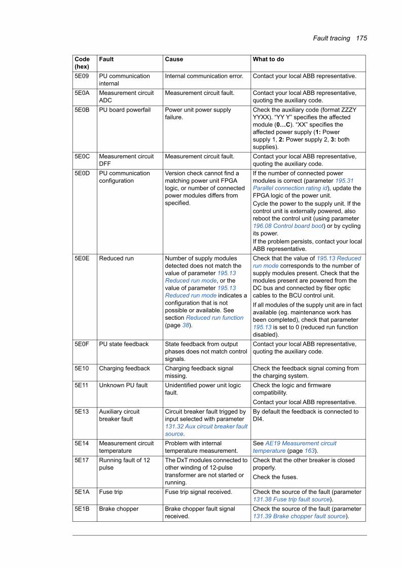
Fault tracing 175
5E09 PU communication internal
Internal communication error. Contact your local ABB representative.
5E0A Measurement circuit ADC
Measurement circuit fault. Contact your local ABB representative, quoting the auxiliary code.
5E0B PU board powerfail Power unit power supply failure.
Check the auxiliary code (format ZZZY YYXX). “YY Y” specifies the affected module (0…C). “XX” specifies the affected power supply (1: Power supply 1, 2: Power supply 2, 3: both supplies).
5E0C Measurement circuit DFF
Measurement circuit fault. Contact your local ABB representative, quoting the auxiliary code.
5E0D PU communication configuration
Version check cannot find a matching power unit FPGA logic, or number of connected power modules differs from specified.
If the number of connected power modules is correct (parameter 195.31 Parallel connection rating id), update the FPGA logic of the power unit.Cycle the power to the supply unit. If the control unit is externally powered, also reboot the control unit (using parameter 196.08 Control board boot) or by cycling its power.If the problem persists, contact your local ABB representative.
5E0E Reduced run Number of supply modules detected does not match the value of parameter 195.13 Reduced run mode, or the value of parameter 195.13 Reduced run mode indicates a configuration that is not possible or available. See section Reduced run function (page 38).
Check that the value of 195.13 Reduced run mode corresponds to the number of supply modules present. Check that the modules present are powered from the DC bus and connected by fiber optic cables to the BCU control unit.
If all modules of the supply unit are in fact available (eg. maintenance work has been completed), check that parameter 195.13 is set to 0 (reduced run function disabled).
5E0F PU state feedback State feedback from output phases does not match control signals.
Contact your local ABB representative, quoting the auxiliary code.
5E10 Charging feedback Charging feedback signal missing.
Check the feedback signal coming from the charging system.
5E11 Unknown PU fault Unidentified power unit logic fault.
Check the logic and firmware compatibility.
Contact your local ABB representative.
5E13 Auxiliary circuit breaker fault
Circuit breaker fault trigged by input selected with parameter 131.32 Aux circuit breaker fault source.
By default the feedback is connected to DI4.
5E14 Measurement circuit temperature
Problem with internal temperature measurement.
See AE19 Measurement circuit temperature (page 163).
5E17 Running fault of 12 pulse
The DxT modules connected to other winding of 12-pulse transformer are not started or running.
Check that the other breaker is closed properly.
Check the fuses.
5E1A Fuse trip Fuse trip signal received. Check the source of the fault (parameter 131.38 Fuse trip fault source).
5E1B Brake chopper Brake chopper fault signal received.
Check the source of the fault (parameter 131.39 Brake chopper fault source).
Code (hex)
Fault Cause What to do

176 Fault tracing
6E00 FPGA version incompatible
Firmware and FPGA file version in the power unit are incompatible.
Reboot the control unit (using parameter 196.08 Control board boot) or by cycling power. If the problem persists, contact your local ABB representative.
Update of power unit logic failed.
Retry.
6E01 FBA A mapping file Fieldbus adapter A mapping file read error.
Contact your local ABB representative.
6E02 FBA B mapping file Fieldbus adapter B mapping file read error.
Contact your local ABB representative.
6E03 Task overload Internal fault.
Note: This fault cannot be reset.
Reboot the control unit (using parameter 196.08 Control board boot) or by cycling power. If the problem persists, contact your local ABB representative.
6E04 Stack overflow Internal fault.
Note: This fault cannot be reset.
Reboot the control unit (using parameter 196.08 Control board boot) or by cycling power. If the problem persists, contact your local ABB representative.
6E05 Internal file load File read error.
Note: This fault cannot be reset.
Reboot the control unit (using parameter 196.08 Control board boot) or by cycling power. If the problem persists, contact your local ABB representative.
6E06 Internal record load Internal record load error. Contact your local ABB representative.
6E07 Application loading Application file incompatible or corrupted.
Note: This fault cannot be reset.
Contact your local ABB representative.
6E08 Memory unit detached The memory unit was detached when the control unit was powered.
Switch off the power to the control unit and reinstall the memory unit.In case the memory unit was not actually removed when the fault occurred, check that the memory unit is properly inserted into its connector and its mounting screw is tight. Reboot the control unit (using parameter 196.08 Control board boot) or by cycling power. If the problem persists, contact your local ABB representative.
6E09 Internal SSW fault Internal fault. Reboot the control unit (using parameter 196.08 Control board boot) or by cycling power. If the problem persists, contact your local ABB representative.
6E0A User set fault Loading of the user parameter set failed because
• requested set does not exist
• set is not compatible with the control program
• supply unit was switched off during loading.
Ensure that a valid user parameter set exists. Reload.
6E0B Kernel overload Operating system error.
Note: This fault cannot be reset.
Reboot the control unit (using parameter 196.08 Control board boot) or by cycling power. If the problem persists, contact your local ABB representative.
6E0C Parameter system Parameter load or save failed. Try forcing a save using parameter 196.07 Parameter save manually. Retry.
Code (hex)
Fault Cause What to do

Fault tracing 177
6E0D FBA A parameter conflict
The diode supply unit does not have a functionality requested by PLC, or requested functionality has not been activated.
Check PLC programming.
Check settings of parameter groups 150 FBA and 151 FBA A settings.
6E0E FBA B parameter conflict
The diode supply unit does not have a functionality requested by PLC, or requested functionality has not been activated.
Check PLC programming.
Check settings of parameter groups 150 FBA and 154 FBA B settings.
6E15 Text data overflow Internal fault. Reset the fault. Contact your local ABB representative if the fault persists.
6E16 Text 32-bit table overflow
Internal fault. Reset the fault. Contact your local ABB representative if the fault persists.
6E17 Text 64-bit table overflow
Internal fault. Reset the fault. Contact your local ABB representative if the fault persists.
6E18 Text file overflow Internal fault. Reset the fault. Contact your local ABB representative if the fault persists.
6E1A Rating ID fault Rating ID load error. Contact your local ABB representative.
6E1B Backup/Restore Timeout
A control panel or PC tool fails to communicate with the drive during backup or restoring operation.
Check the control panel or PC tool communication, and if it is still in backup/restore state.
6E1C Emergency stop fault Diode supply unit has received an emergency stop command.
Check that it is safe to continue operation.
Return the emergency stop pushbutton to normal position.
Restart the supply unit.
6E1D Internal SW error Internal error. Contact your local ABB representative. Quote the auxiliary code (check the event details in the event log).
6E1F Licensing fault Running the control program is prevented either because a restrictive license exists, or because a required license is missing.
Record the auxiliary codes of all active licensing faults and contact your product vendor for further instructions.
6E20 Fault reset Fault reset has been requested and done.
Informative fault.
7E00 Option module comm loss
Communication between the diode supply unit and an option module is lost.
Check that the option modules are properly seated in their slots.Check that the option modules or slot connectors are not damaged. To pinpoint the problem, try installing the modules into different slots.
7E01 Panel lossProgrammable fault: 149.05 Communication loss action
Control panel (or PC tool) has stopped communicating.
Check PC tool or control panel connection.Check control panel connector.Disconnect and reconnect the control panel.Check the auxiliary code. The code specifies the I/O port used as follows: 0: Panel, 1: Fieldbus interface A, 2: Fieldbus interface B, 3: Ethernet, 4: D2D/EFB port).
Code (hex)
Fault Cause What to do

178 Fault tracing
7E0B FBA A communicationProgrammable fault: 150.02 FBA A comm loss func
Cyclical communication between diode supply unit and fieldbus adapter module A or between PLC and fieldbus adapter module A is lost.
Check status of fieldbus communication. See user documentation of fieldbus interface.
Check settings of parameter groups 150 FBA, 151 FBA A settings, 152 FBA A data in and 153 FBA A data out.
Check cable connections.
Check if communication master is able to communicate.
7E0C FBA B communicationProgrammable fault: 150.32 FBA B comm loss func
Cyclical communication between diode supply unit and fieldbus adapter module B or between PLC and fieldbus adapter module B is lost.
Check status of fieldbus communication. See user documentation of fieldbus interface.
Check settings of parameter groups 150 FBA, 154 FBA B settings, 155 FBA B data in and 156 FBA B data out.
Check cable connections.
Check if communication master is able to communicate.
7E10 Ext I/O comm loss The I/O extension module types specified by parameters do not match the detected configuration.
Check the event log for an auxiliary code (format XXYY YYYY). “XX” specifies the number of the I/O extension module (01: parameter group 114 Extension I/O module 1, 02: 115 Extension I/O module 2, 03: 116 Extension I/O module 3).
“YY YYYY” indicates the problem (see actions for each code below).
00 0001 Communication with module
failed.
Check that the module is properly seated in its slot.
Check that the module and the slot connector is not damaged.
Try installing the module into another slot.
00 0002 Module not found. Check the type and location settings of the modules (parameters 114.01/114.02, 115.01/115.02 or 116.01/116.02).
Check that the module is properly seated in its slot.
Check that the module and the slot connector is not damaged.
Try installing the module into another slot.
00 0003 Configuration of module failed.
00 0004 Configuration of module failed.
7E11 DDCS controller comm lossProgrammable fault: 160.59 DDCS controller comm loss action
DDCS (fiber optic) communication between the supply unit and external controller is lost.
Check status of controller. See the user documentation of the controller.
Check settings of parameter group 160 DDCS communication.
Check cable connections. If necessary, replace cables.
7E13 Incompatible option module
Option module not supported. (For example, type Fxxx-xx-M fieldbus adapter modules are not supported.)
Check the auxiliary code. The code specifies the interface to which the unsupported module is connected: 1: Fieldbus interface A, 2: Fieldbus interface B.Replace the module with a supported type.
Code (hex)
Fault Cause What to do

Fault tracing 179
8E00 Overvoltage Grid voltage is above 120% of the parameter 195.01 Supply voltage for more than 0.5 seconds.
Check that parameter 195.01 Supply voltage is set according to the supply voltage in use.
Check the auxiliary code to identify the diode supply unit (15: single diode supply unit or the first parallel-connected diode supply unit, 16: the second parallel-connected diode supply unit).
8E06 AI supervisionProgrammable fault: 112.03 AI supervision function
An analog signal is outside the limits specified for the analog input.
Check the event log for an auxiliary code (format XXXX XYZZ). “Y” specifies the location of the input (0: Control unit, 1: I/O extension module 1, 2: I/O extension module 2, 3: I/O extension module 3). “ZZ” specifies the limit (01: AI1 under minimum, 02: AI1 above maximum, 03: AI2 under minimum, 04: AI2 above maximum).Check signal level at the analog input.Check the wiring connected to the input.Check the minimum and maximum limits of the input in parameter group 112 Standard AI.
9E01 External fault 1(Editable message text)Programmable fault: 131.01 External event 1 source131.02 External event 1 type
Fault in external device 1. Check the external device.
Check setting of parameter 131.01 External event 1 source.
9E02 External fault 2(Editable message text)Programmable fault: 131.03 External event 2 source131.04 External event 2 type
Fault in external device 2. Check the external device.Check setting of parameter 131.03 External event 2 source.
9E03 External fault 3(Editable message text)Programmable fault: 131.05 External event 3 source131.06 External event 3 type
Fault in external device 3. Check the external device.Check setting of parameter 131.05 External event 3 source.
9E04 External fault 4(Editable message text)Programmable fault: 131.07 External event 4 source131.08 External event 4 type
Fault in external device 4. Check the external device.Check setting of parameter 131.07 External event 4 source.
9E05 External fault 5(Editable message text)Programmable fault: 131.09 External event 5 source131.10 External event 5 type
Fault in external device 5. Check the external device.Check setting of parameter 131.09 External event 5 source.
FE00 FB A force trip A fault trip command has been received through fieldbus adapter A.
Check the fault information provided by the PLC.
Code (hex)
Fault Cause What to do

180 Fault tracing
FE01 FB B force trip A fault trip command has been received through fieldbus adapter B.
Check the fault information provided by the PLC.
FE03 Safe torque off 1 loss Some STO connectors are not connected.
Note: In diode supply units the STO connectors do not constitute a true safety function.
Check the auxiliary code. The code contains location information, especially with parallel-connected modules. When converted into a 32-bit binary number, the bits of the code indicate the following:31…28: Number of faulty module (0…11 decimal). 1111: STO_ACT states of control unit and modules in conflict27: STO_ACT state of modules26: STO_ACT state of control unit25: STO1 of control unit24: STO2 of control unit23…12: STO1 of modules 12…1 (Bits of non-existing modules set to 1)11…0: STO2 of modules 12…1 (Bits of non-existing modules set to 1)
FE04 Safe torque off 2 loss Some STO connectors are not connected.
Note: In diode supply units the STO connectors do not constitute a true safety function.
Code (hex)
Fault Cause What to do

Fieldbus control through a fieldbus adapter 181
8
Fieldbus control through a fieldbus adapter
What this chapter containsThis chapter describes how the supply unit can be controlled by external devices over a communication network (fieldbus) through an optional fieldbus adapter module.

182 Fieldbus control through a fieldbus adapter
System overviewThe user can control the diode supply unit through a fieldbus interface if the unit is equipped with an optional fieldbus adapter (for example, option +K454). Then the supply unit can be connected to an external control system through a serial communication link. The fieldbus adapter can be installed into any free slot on the control unit.
The diode supply unit can be set to receive its control information through the fieldbus interface, or the control can be distributed between the fieldbus interface and other available sources such as digital and analog inputs.
Fieldbus adapters are available for various serial communication systems and protocols, for example• CANopen (FCAN-01 adapter)
• ControlNet (FCNA-01 adapter)
• DeviceNet (FDNA-01 adapter)
• EtherCAT (FECA-01 adapter)
• EtherNet/IP (FENA-11 or FENA-21 adapter)
• Modbus/RTU (FSCA-01 adapter)
• Modbus/TCP (FENA-11 or FENA-21 adapter)
• POWERLINK (FEPL-02 adapter)
• PROFIBUS DP (FPBA-01 adapter)
• PROFINET IO (FENA-11 or FENA-21 adapter).
Note: The text and examples in this chapter describe the configuration of one fieldbus adapter (FBA A) by parameters 150.01…150.21 and parameter groups 151…153. The second adapter (FBA B), if present, is configured in a similar fashion by parameters 150.31…150.51 and parameter groups 154…156.
Data Flow
Process I/O (cyclic)
Process I/O (cyclic) or Service messages (acyclic)
Control word (CW)
Fieldbus controller
Parameter R/W requests/responses
Status word (SW)
Actual values
Fieldbus
Other devices
ACS880
Type Fxxx fieldbus adapter installed on the control unit

Fieldbus control through a fieldbus adapter 183
Note: If FENA-xx Ethernet adapter is used for Ethernet tool network and Drive composer PC tool, use the FENA-xx adapter as fieldbus adapter B. Configure the FENA-xx adapter through parameters 150.31…150.51 and parameter groups 154…156. Normally, use the fieldbus adapter module as fieldbus adapter A. See Ethernet tool network for ACS880 drives application guide (3AUA0000125635 [English]), and FENA-01/-11 Ethernet adapter module user’s manual (3AUA0000093568 [English]).
Basics of the fieldbus control interfaceThe cyclic communication between a fieldbus system and the diode supply unit consists of 16/32-bit input and output data words. The diode supply unit supports at the maximum the use of 12 data words (16 bits) in each direction.
Data transmitted from the diode supply unit to the fieldbus controller is defined by parameters 152.01 FBA A data in1 … 152.12 FBA A data in12. The data transmitted from the fieldbus controller to the diode supply unit is defined by parameters 153.01 FBA data out1 … 153.12 FBA data out12.
Control word and Status word
The Control word is the principal means for controlling the diode supply unit from a fieldbus system. It is sent by the fieldbus master station to the diode supply unit through the adapter module. The diode supply unit switches between its states according to the bit-coded instructions on the Control word, and returns status information to the master in the Status word.
The contents of the Control word and the Status word are detailed on pages 184 and 186 respectively.
If parameter 150.12 FBA A debug mode is set to Fast, the Control word received from the fieldbus is shown by parameter 150.13 FBA A control word, and the Status word transmitted to the fieldbus network by 150.16 FBA A status word.
Actual values
Actual values are 16-bit words containing information on the operation of the diode supply unit.
If parameter 150.12 FBA A debug mode is set to Fast, the actual values sent to the fieldbus are displayed by 150.17 FBA A actual value 1 and 150.18 FBA A actual value 2.

184 Fieldbus control through a fieldbus adapter
Contents of the fieldbus Control word
Bit Name Value Description
0 ON/OFF 1 DxD modules: If either ON/OFF (bit 0) or Start (bit 3) is 1:
1. Switch on the charging contactor
2. Charge.
3. Switch off the charging contactor, and switch on the main contactor/breaker. Charging is not in use in all units. See section Charging of DxD supply unit on page 35.
DxT modules: If either ON/OFF (bit 0) or Start (bit 3) is 1:
1. Close the main contactor/breaker and charge the DC busbar.
2. Ready to operate.
0 If both ON/OFF (bit 0) or Start (bit 3) is 0:
Switch off the charging contactor and the main contactor/breaker.
1 Off2 control 1 Continue operation (OFF2 inactive)
0 Emergency stop, open main contactor
2 Off3 control 1 Continue operation (OFF3 inactive)
0 Emergency stop, open main contactor
3 Start 1 DxD modules: If either ON/OFF (bit 0) or Start (bit 3) is 1:
1. Switch on the charging contactor
2. Charge.
3. Switch off the charging contactor, and switch on the main contactor/breaker. Charging is not in use in all units. See section Charging of DxD supply unit on page 35.
DxT modules: If either ON/OFF (bit 0) or Start (bit 3) is 1:
1. Close the main contactor/breaker and charge the DC busbar.
2. Ready to operate.
0 If both Run (bit 0) or Start (bit 3) is 0:
Switch off the charging contactor and the main contactor/breaker.
4 - 1 Not in use.
0 Not in use.
5 - 1 Not in use.
0 Not in use.
6 - 1 Not in use.
0 Not in use.
7 Reset 0=>1 Fault reset if an active fault exists.
0 - (no reset)
8 - 1 Not in use.
0 Not in use.
9 - 1 Not in use.
0 Not in use.
10 Remote cmd 1 Control location: REMOTE (EXT1 or EXT2).
0 Control location: LOCAL.
11 Ext ctrl loc 1 Select External Control Location EXT2. Effective if control location is parameterized to be selected from fieldbus.
0 Select External Control Location EXT1. Effective if control location is parameterized to be selected from fieldbus.
12 User bit 0 1 User bit 0 from external control location.
0 User bit 0 from external control location.

Fieldbus control through a fieldbus adapter 185
13 User bit 1 1 User bit 1 from external control location.
0 User bit 1 from external control location.
14 User bit 2 1 User bit 2 from external control location.
0 User bit 2 from external control location.
15 User bit 3 1 User bit 3 from external control location.
0 User bit 3 from external control location.
Bit Name Value Description

186 Fieldbus control through a fieldbus adapter
Contents of the fieldbus Status word
Bit Name Value Description
0 Ready to switch ON
1 Ready to switch ON
Note: If the supply unit is switched off, the Start enable must be on for Ready to switch ON = 1. If the supply unit is switched on, Ready to switch ON = 1 regardless of the Start enable.
0 Not ready to switch ON
1 Ready run 1 Ready to operate. Start command is on and main contactor is closed.
0 Start command is not given or main contactor is open.
2 Ready ref 1 Operation enabled
0 Operation inhibited
3 Tripped 1 Fault
0 No fault active
4 - 1 Not in use.
0 Not in use.
5 - 1 Not in use.
0 Not in use.
6 - 1 Not in use.
0 Not in use.
7 Warning 1 A warning is active
0 No warnings active
8 Operating 1 Thyristors of the DxT module are modulating, during charging or when the supply unit is running. During charging, thyristors are already conducting, but DC voltage has not yet risen to ‘Ready ref’ level.
0 Thyristors of the DxT module are not modulating.
9 Remote 1 Control location: REMOTE (EXT1 or EXT2).
0 Control location: LOCAL.
10 Ready for load 1 Ready for load.
0 Not ready for load.
11 User bit 0 1 See parameter 106.30 MSW bit 11 sel.
0 See parameter 106.30 MSW bit 11 sel.
12 User bit 1 1 See parameter 106.31 MSW bit 12 sel.
0 See parameter 106.31 MSW bit 12 sel.
13 User bit 2 1 See parameter 106.32 MSW bit 13 sel.
0 See parameter 106.32 MSW bit 13 sel.
14 Charging 1 Charging state is active. See section Charging of DxD supply unit on page 35.
0 Charging state is not active. See section Charging of DxD supply unit on page 35.
15 User bit 3 1 See parameter 106.33 MSW bit 15 sel.
0 See parameter 106.33 MSW bit 15 sel.

Fieldbus control through a fieldbus adapter 187
The state diagram
POWER ON
SWITCH-ON INHIBITED
READY TO SWITCH ON
OPERATION ENABLED
FAULT
from any state
Notation:
xxx: Any bit value combination.
SW: 106.11 Main status word
CW: 106.01 Main control word
SWITCH-ON INHIBITED SW = xxxx xxxx xxxx 0000
Interlockings prevent starting and charging.
READY TO SWITCH ON SW = xxxx xxxx xxxx 0001Main contactor open. No active interlockings that would prevent starting or charging.
OPERATION ENABLED SW = xxxx xxxx xxxx 0111
Charged and running. If DxD converter is equipped with an external charging circuit, SW = x1xx xxxx xxxx 0001 is shown during charging phase shortly before entering the operation enabled state.
FAULT SW = xxxx xxxx xxxx 1000
Modulation stopped and main contactor open.
run enable = 1
FAULT
FAULT RESET
run enable = 0CW = x111or 111x
CW = 0xx0

188 Fieldbus control through a fieldbus adapter
Setting up the diode supply unit for fieldbus controlBefore configuring the diode supply unit for fieldbus control, the adapter module must be mechanically and electrically installed according to the instructions given in the User’s manual of the appropriate fieldbus adapter module.
Note: To be able to switch the main contactor and the supply unit on and off through the fieldbus, the Run enable command at the digital input DI2 (by default) must be on (1). That is the case when the operating switch [S11] is switched to the on (1) position.
1. Power up the diode supply unit.
2. Enable the communication between the diode supply unit and the fieldbus adapter module by setting parameter 150.01 FBA A enable to Option slot 1.
3. With 150.02 FBA A comm loss func, select how the diode supply unit should react to a fieldbus communication break.Note: This function monitors both the communication between the fieldbus master and the adapter module and the communication between the adapter module and the diode supply unit.
4. With 150.03 FBA A comm loss t out, define the time between communication break detection and the selected action.
5. Select application-specific values for the rest of the parameters in group 150 FBA.
6. Set the fieldbus adapter module configuration parameters in group 151 FBA A settings. At the minimum, set the required node address and the communication profile. Set profile to transparent 16 mode.Note: The parameter indexes and names vary as the way the different fieldbus adapters use these parameters.Example: For the FPBA adapter, set parameter 151.05 Profile to mode Trans16.
7. Define the process data transferred to and from the diode supply unit in parameter groups 152 FBA A data in and 153 FBA A data out.Note: The adapter module sets the Status word and Control word automatically into parameters 152.01 and 153.01 respectively.
8. Save the valid parameter values to permanent memory by setting parameter 196.07 Parameter save manually to Save.
9. Validate the settings made in parameter groups 151, 152 and 153 by setting parameter 151.27 FBA A par refresh to Configure.
10. Select the fieldbus adapter A as the source of the start and stop commands for external control location EXT1 by setting parameter 120.01 Ext1 commands to Fieldbus A.
11. Set the relevant control parameters to control the diode supply unit according to the application.

Fieldbus control through a fieldbus adapter 189
Setting up the communication between DSU and inverter unitConnect the fiber optic cables between the DDCS communication port of the inverter unit (parameter 60.71 INU-LSU communication port) and the DDCS controller port of the DSU (parameter 160.51 DDCS controller comm port). For example, in the DSU, slot 3A is used with the ZCU control unit and, in the inverter unit, channel CH1 of the RDCO connector unit in the BCU-x2 control unit.
In ACS880-07 drives, setting the DSU parameter 195.20 HW options word 1 bit 11 to Yes automatically sets the following DSU parameters to their right values:
In ACS880-07 drives, setting the INU parameter 95.20 HW options word 1 bit 11 to Yes automatically sets the following INU parameters to their right values:
In the diode supply unit, data transmitted from the diode supply unit is defined with parameters 161.51 Data set 11 data 1 selection…161.74 Data set 25 data 3 selection. Data is received using parameters 162.51 Data set 10 data 1 selection…162.74 Data set 24 data 3 selection.
In the inverter unit, data transmitted to the diode supply unit is defined with parameters 61.151…61.186. Data is received using parameters 62.151…62.174.
With the settings above, the inverter unit controls the diode supply unit. In other words, the diode supply unit receives the Control word from the inverter unit and transmits the Status word to the inverter unit.
Note: The control program still requires the Run enable command from digital input DI2 (by default) which is normally wired to the DSU door switch.
DSU parameter Setting
120.01 Ext1 commands DDCS controller
120.02 Ext1 start trigger Level
120.12 Run enable 1 DI2
160.58 DDCS controller comm loss time Set time, eg. 100 ms.
160.51 DDCS controller comm port Set port to be used. Eg. slot 3A is used with the ZCU control unit, and RDCO CH0 is used with the BCU control unit.
161.51 Data set 11 data 1 selection SW 16bit
162.51 Data set 10 data 1 selection CW 16bit
Inverter unit parameter Setting
60.71 INU-LSU communication port RDCO CH1
60.81 LSU control On
61.151 INU-LSU data set 10 data 1 sel LSU CW
62.151 INU-LSU data set 11 data 1 sel SW 16bit

190 Fieldbus control through a fieldbus adapter

Drive-to-drive link 191
9
Drive-to-drive link
This feature is not supported by the current firmware version.

192 Drive-to-drive link

Further information
Product and service inquiries
Address any inquiries about the product to your local ABB representative, quoting the type designation and serial number of the unit in question. A listing of ABB sales, support and service contacts can be found by navigating to www.abb.com/searchchannels.
Product training
For information on ABB product training, navigate to new.abb.com/service/training.
Providing feedback on ABB manuals
Your comments on our manuals are welcome. Navigate to new.abb.com/drives/manuals-feedback-form.
Document library on the Internet
You can find manuals and other product documents in PDF format on the Internet at www.abb.com/drives/documents.

Contact us
www.abb.com/driveswww.abb.com/drivespartners
3AUA0000103295 Rev F (EN) 2017-06-09