EMS 4.0 pull s together - The MESSUI Place
32
EMS 4.0 pull s together In search of supernumerary memory for DOS applications, EMS 4.0 unites something old, something borrowed, and something new, says Ted Mirecki. Until applications arrive that fulfill the promise of OS/2, many users are sear- ching for alternatives that can run widely available DOS applications, yet over- come the limitations of that operating system. Expanded memory is the tech- nology that gives such alternatives a large part of their power. The Lotus/- Intel/Microsoft Expanded Memory Specification (EMS) version 4.0 unites features of earlier EMS versions with strengths of the AST Research/Quad- ram/Ashton-Tate Enhanced Expanded Memory Specification (EEMS), and it adds some traits of its own to create a new and improved EMS. The new ver- sion may open all kinds of doors for DOS applications. Lotus, Intel and Microsoft originally developed EMS to relieve the spread- sheet power user's memory crunch. It was intended to provide 8Mbytes of memory beyond the 640k limit as a repository for data such as spreadsheet cells or a RAM disk. Because most programs of this type already provided their own data space management, ex- panded-memory management was also left at the application level. Therefore, expanded memory benefited applica- tions only to the extent that they were written specifically to take advantage of it. Such applications and utilities soon proliferated. However, DOS systems needed addi- tional memory for purposes other than data storage. Programs were growing in size, and users were discovering multi- tasking in the form of terminate-and- stay-resident (TSR) utilities and task- switching environments that loaded more than one program at a time. Al- though the original EMS offered the pos- sibility of expanding the memory space by an order of magnitude, the design of its hardware interface with the rest of the system made it inefficient for running multiple programs. To provide for this further use of ex- panded memory, AST, Quadram, and Ashton-Tate developed EEMS. For ap- plications and small TSR utilities, EEMS provides the same capabilities, in the same way as EMS. For system-level control programs that create and manage task-switching or multi-tasking environments, it efficiently expands memory available for running programs. The most notable EEMS success is DESQview from . Quarterdeck Office Sys- tems. DESQview and Microsoft Win- dows run on top of DOS and rely on a hardware solution to expanded memory. Either of these, in conjunction with un- derlying hardware, can provide two fea- tures lacking in DOS: a large address space and multi-tasking. Quarterdeck's windowing multi-tasking environment is much like Microsoft Win- dows, but it is text-based and menu- driven instead of graphics- and icon- oriented. It can simultaneously run — not just hold in memory for task switch- ing but actually execute — as many programs as will fit in available ex- panded memory. By comparison, Win- dows versions prior to 2.0 used EMS memory for data storage only, so it could multi-task only as many programs as fit in the 640k of conventional memory space at one time. DESQview demonstrated that ex- panded memory could go beyond mere- ly providing data storage space. In recognition of this fact, Lotus, Intel, and Microsoft revised their specification ex- tensively to create EMS 4.0. The major changes are increasing the maximum expanded memory space from 8Mbytes to 32Mbytes, incorporating the same hardware interface as EEMS, and ad- ding multi-tasking support in software. Part of the motivation for this revision was undoubtedly the release of Win- dows 2.0, which takes advantage of the multi-tasking support provided by EMS 4.0 software running on appropriate hardware. Another reason could have been the design of IBM's 80286 Memory Expanded board for the PS/2 Models 50 and 60, which supports a mapping scheme functionally equivalent to EEMS APC August 1988 Page 207
Transcript of EMS 4.0 pull s together - The MESSUI Place

EMS 4.0 pulls together
In search of supernumerary memory for DOS applications, EMS 4.0 unites something old, something borrowed, and something
new, says Ted Mirecki.
Until applications arrive that fulfill the promise of OS/2, many users are sear-ching for alternatives that can run widely available DOS applications, yet over-come the limitations of that operating system. Expanded memory is the tech-nology that gives such alternatives a large part of their power. The Lotus/- Intel/Microsoft Expanded Memory Specification (EMS) version 4.0 unites features of earlier EMS versions with strengths of the AST Research/Quad-ram/Ashton-Tate Enhanced Expanded Memory Specification (EEMS), and it adds some traits of its own to create a new and improved EMS. The new ver-sion may open all kinds of doors for DOS applications.
Lotus, Intel and Microsoft originally developed EMS to relieve the spread-sheet power user's memory crunch. It was intended to provide 8Mbytes of memory beyond the 640k limit as a repository for data such as spreadsheet cells or a RAM disk. Because most programs of this type already provided their own data space management, ex-panded-memory management was also left at the application level. Therefore, expanded memory benefited applica-tions only to the extent that they were written specifically to take advantage of it. Such applications and utilities soon proliferated.
However, DOS systems needed addi-tional memory for purposes other than data storage. Programs were growing in size, and users were discovering multi-tasking in the form of terminate-and-stay-resident (TSR) utilities and task-switching environments that loaded more than one program at a time. Al-though the original EMS offered the pos-sibility of expanding the memory space by an order of magnitude, the design of its hardware interface with the rest of the system made it inefficient for running multiple programs.
To provide for this further use of ex-panded memory, AST, Quadram, and Ashton-Tate developed EEMS. For ap-plications and small TSR utilities, EEMS provides the same capabilities, in the same way as EMS. For system-level control programs that create and manage task-switching or multi-tasking environments, it efficiently expands memory available for running programs.
The most notable EEMS success is DESQview from. Quarterdeck Office Sys-tems. DESQview and Microsoft Win-dows run on top of DOS and rely on a hardware solution to expanded memory. Either of these, in conjunction with un-derlying hardware, can provide two fea-tures lacking in DOS: a large address space and multi-tasking.
Quarterdeck's windowing multi-tasking
environment is much like Microsoft Win-dows, but it is text-based and menu-driven instead of graphics- and icon-oriented. It can simultaneously run — not just hold in memory for task switch-ing but actually execute — as many programs as will fit in available ex-panded memory. By comparison, Win-dows versions prior to 2.0 used EMS memory for data storage only, so it could multi-task only as many programs as fit in the 640k of conventional memory space at one time.
DESQview demonstrated that ex-panded memory could go beyond mere-ly providing data storage space. In recognition of this fact, Lotus, Intel, and Microsoft revised their specification ex-tensively to create EMS 4.0. The major changes are increasing the maximum expanded memory space from 8Mbytes to 32Mbytes, incorporating the same hardware interface as EEMS, and ad-ding multi-tasking support in software.
Part of the motivation for this revision was undoubtedly the release of Win-dows 2.0, which takes advantage of the multi-tasking support provided by EMS 4.0 software running on appropriate hardware. Another reason could have been the design of IBM's 80286 Memory Expanded board for the PS/2 Models 50 and 60, which supports a mapping scheme functionally equivalent to EEMS
APC August 1988 Page 207
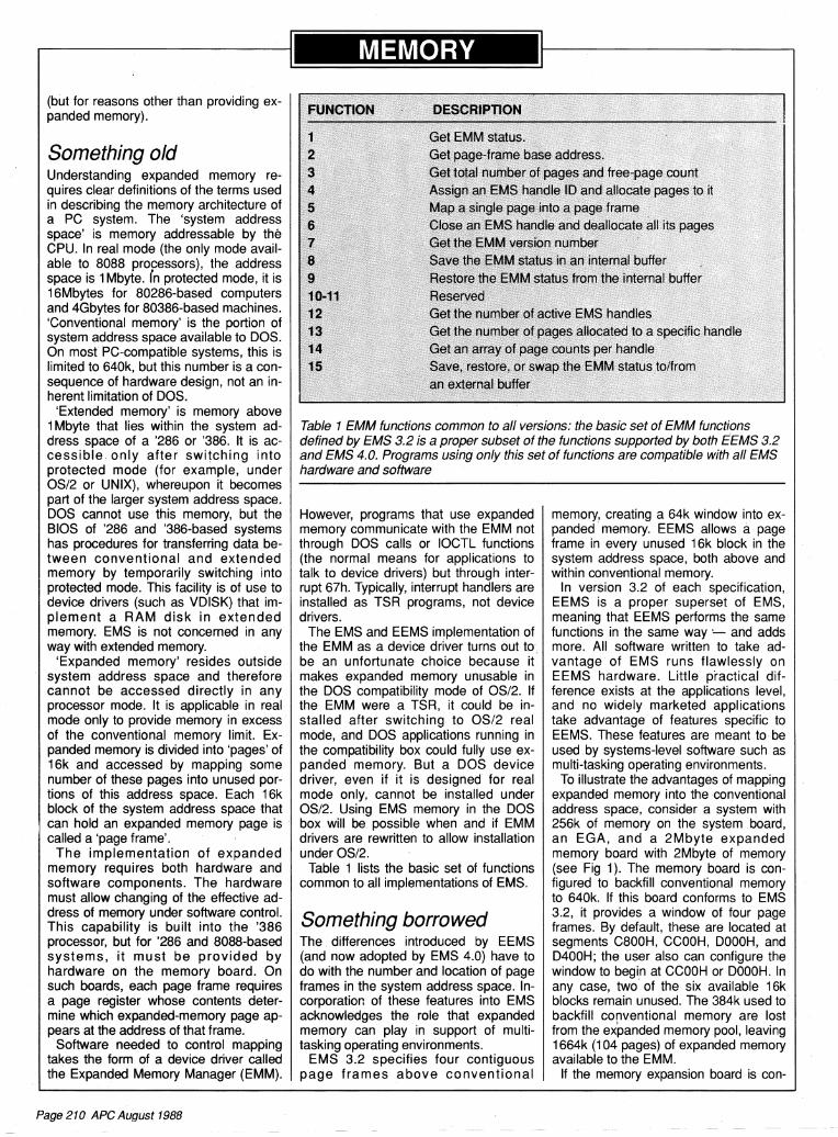
)ESCRIPTION
Get EMM status. Get page-frame base address.' Get total number of pages and free-pae count Assign an EMS handle lD 'and allocate pagges to it Map a single page into a page frame Close an EMS'hadle and deallocate all its pages Get the EIM version number Save the EMM status in an internal buffer Restore the EIM status from the internal buffer Reserved !0!",:4017!-m?!!r:of active EMS handles po?Foo:,!p"r!"poip!gOgOgii!lk01#t001,td,a:i,:t;).0ifplpilqt" Get an array of page counts per handle Save restore, or swap the ElM status to/f ror an external buffer
FUNCTION
Table 1 EMM functions common to all versions: the basic set of EMM functions defined by EMS 3.2 is a proper subset of the functions supported by both EEMS 3.2 and EMS 4.0. Programs using only this set of functions are compatible with all EMS hardware and software
(but for reasons other than providing ex-panded memory).
Something old Understanding expanded memory re-quires clear definitions of the terms used in describing the memory architecture of a PC system. The 'system address space' is memory addressable by the CPU. In real mode (the only mode avail-able to 8088 processors), the address space is 1Mbyte. (n protected mode, it is 16Mbytes for 80286-based computers and 4Gbytes for 80386-based machines. `Conventional memory' is the portion of system address space available to DOS. On most PC-compatible systems, this is limited to 640k, but this number is a con-sequence of hardware design, not an in-herent limitation of DOS.
`Extended memory' is memory above 1Mbyte that lies within the system ad-dress space of a '286 or '386. It is ac-cessible only after switching into protected mode (for example, under OS/2 or UNIX), whereupon it becomes part of the larger system address space. DOS cannot use this memory, but the BIOS of '286 and '386-based systems has procedures for transferring data be-tween conventional and extended memory by temporarily switching into protected mode. This facility is of use to device drivers (such as VDISK) that im-plement a RAM disk in extended memory. EMS is not concerned in any way with extended memory.
`Expanded memory' resides outside system address space and therefore cannot be accessed directly in any processor mode. It is applicable in real mode only to provide memory in excess of the conventional memory limit. Ex-panded memory is divided into 'pages' of 16k and accessed by mapping some number of these pages into unused por-tions of this address space. Each 16k block of the system address space that can hold an expanded memory page is called a 'page frame'.
The implementation of expanded memory requires both hardware and software components. The hardware must allow changing of the effective ad-dress of memory under software control. This capability is built into the '386 processor, but for '286 and 8088-based systems, it must be provided by hardware on the memory board. On such boards, each page frame requires a page register whose contents deter-mine which expanded-memory page ap-pears at the address of that frame.
Software needed to control mapping takes the form of a device driver called the Expanded Memory Manager (EMM).
However, programs that use expanded memory communicate with the EMM not through DOS calls or IOCTL functions (the normal means for applications to talk to device drivers) but through inter-rupt 67h. Typically, interrupt handlers are installed as TSR programs, not device drivers.
The EMS and EEMS implementation of the EMM as a device driver turns out to be an unfortunate choice because it makes expanded memory unusable in the DOS compatibility mode of OS/2. If the EMM were a TSR, it could be in-stalled after switching to OS/2 real mode, and DOS applications running in the compatibility box could fully use ex-panded memory. But a DOS device driver, even if it is designed for real mode only, cannot be installed under OS/2. Using EMS memory in the DOS box will be possible when and if EMM drivers are rewritten to allow installation under OS/2.
Table 1 lists the basic set of functions common to all implementations of EMS.
Something borrowed The differences introduced by EEMS (and now adopted by EMS 4.0) have to do with the number and location of page frames in the system address space. In-corporation of these features into EMS acknowledges the role that expanded memory can play in support of multi-tasking operating environments.
EMS 3.2 specifies four contiguous page frames above conventional
memory, creating a 64k window into ex-panded memory. EEMS allows a page frame in every unused 16k block in the system address space, both above and within conventional memory.
In version 3.2 of each specification, EEMS is a proper superset of EMS, meaning that EEMS performs the same functions in the same way = and adds more. All software written to take ad-vantage of EMS runs flawlessly on EEMS hardware. Little practical dif-ference exists at the applications level, and no widely marketed applications take advantage of features specific to EEMS. These features are meant to be used by systems-level software such as multi-tasking operating environments.
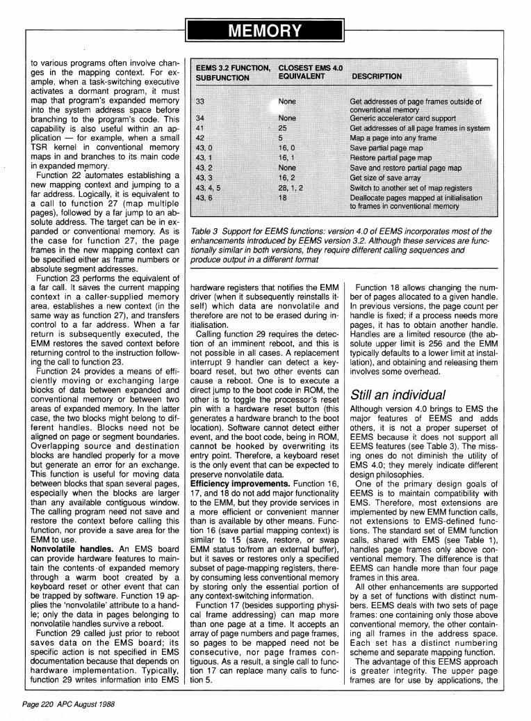
To illustrate the advantages of mapping expanded memory into the conventional address space, consider a system with 256k of memory on the system board, an EGA, and a 2Mbyte expanded memory board with 2Mbyte of memory (see Fig 1). The memory board is con-figured to backfill conventional memory to 640k. If this board conforms to EMS 3.2, it provides a window of four page frames. By default, these are located at segments C800H, CCOOH, DOOOH, and D400H; the user also can configure the window to begin at CCOOH or D000H. In any case, two of the six available 16k blocks remain unused. The 384k used to backfill conventional memory are lost from the expanded memory pool, leaving 1664k (104 pages) of expanded memory available to the EMM.
If the memory expansion board is con-
Page 210 APC August 1988

AdditioN 2 pages
VIDEO BUFFER
Backfilled no page frames
Unused
Primary Window, 4 pages
EMS VERSION
3.2
SEGMENT ADDRESS
10000H r
E000H
D800H
DOOOH
C800H
C000H
256K ON SYSTEM BOARD
384K BACKFILLED
MEMORY SIZE (K) 10.24
EEMS AND EM;, VERSION 4.0
Backfilled, 24 page frames
Primary Window, 4 pages
Fig 1 Example memory configuration: previous versions of EMS were limited to providing four page frames above conventional memory. Version 4.0, like previous versions of EEMS, allows a page frame in any 16k block, above or below 640k, not populated by RAM or ROM
structed to the standards of EEMS 3.2 or EMS 4.0, the primary window at segment C800H can extend over six page frames instead of four, allowing an application to manipulate 96k of expanded memory at a time instead of 64k. In addition, the back-filled memory below 640k supports page frames, allowing the mapping of ex-panded memory pages into conventional memory. Memory used for backfilling remains in the expanded memory pool. While the primary window is meant to be controlled by applications, only an operat-ing system or system-level tasking en-vironment should manage page frames within conventional memory.
If an operating environment running
several. co-resident applications con-sumes the entire conventional memory space, and the user requests start-up of yet another application, a program must be unloaded from memory to make room for the new one. In the absence of ex-panded memory, one of the applications must be written out to disk before a new one is loaded. With EMS memory, the operating environment could copy an ap-plication' into expanded memory with this sequence: 1. Allocate a sufficient number of ex-panded memory pages to hold the un-loaded application. 2. Map four of those pages into the win-dow at segment C800H.
Page 214 APC August 1988

FUNCTION DESCRIPTION
3a v e/Re
s to
re partial artial
p
age
mapap
AaUnnaPmu'tiPepages into page age
fram e
s ,hagenumber o;pages allocated to a handle e 3evetvolatittya;trbuteofahande 3etethandename 3et handle numberforhandlenane
\lter Page maPandjump to a faraddres Ater page maP'call afa1 address,thenrestore Ao\e/Excharge contents of memory' block 3et array of page-frame aae_frare
a
Ad-esses 3etexpandeuiemoryhardvrein f:m
at i) n iiocate Pagesinsizesothertnanlblocks
°ntr°'alternatemaPPing registers 3rePareexPandeum,n°Yhardwarefrwar
warm )isabtelEnabiestem_1ee1EMmfunei°ns
16 17 18 19 20 21 22 23 24 25 26 27 28 29 30
page map
number called the `EMM handle'. To map a page into the system address space, the program identifies it by specifying the handle number and a logi-cal page number ranging from zero to one less than the number of pages allo-cated to that handle. Function 20 allows the assignment of an eight-character name of the user's choice to any handle. The EMM keeps a directory of handle names, and function 21 searches this directory and returns the handle number for a given name. This feature can be used for communication between co-operating programs.
For example, a database program could allocate some pages and store data in them. If the program gives a name to the handle, another program that knows the name (say a word processor or spreadsheet) can find out from the EMM the handle number as-sociated with the name. Knowing the handle, the second program can access the data stored in these pages. The handle number cannot be hard-coded into programs because this number can change at every execution, depending on the order in which various co-resident programs are loaded. Physical page addressing. In previous EMS versions, page frames in the sys-tem address space are identified by frame number. For the configuration shown in Fig 1, the four frames in the primary window are numbered from 0 for the frame at segment C800H, to 3 for the one at D400H. In the EEMS im-
plementation, the first four frames are numbered the same way; frames at D800H and DCOOH are designated as 4 and 5, respectively, and the ones begin-ning at 4000H in conventional memory are numbered from 6 upward. When mapping an expanded memory page, a program specifies its location in the sys-tem address space by supplying the frame number.
For compatibility, version 4.0 accepts the same frame numbering, but function 17 also allows specifying the location of the frame by its physical segment ad-dress. When calling this function to map a page into the lowest frame in conven-tional memory, a program could pass either 4000H or 6 as the frame argu-ment. A subfunction code specifies the argument type.
Function 25 constructs an array of all page-frame addresses 1, the system; it is similar, but not identi .1, to EEMS function 41. Entries in th- .rray re-turned by function 25 are ordere• by physical address and consist of t o words: the segment address and th - frame number. Function 41 returns .n array of bytes containing the hi. • -order six bits of each frame's address; entries are ordered by frame number, with the address for frame N in the Nth byte of the array. The new method is more con-venient for physical addressing of page frames, the old one for addressing them by number. Raw page sizes. The division of ex-panded memory into pages of 16k is not
Table 2 EMM functions added in EMS 4.0: the new EMS 4.0 functions that support the hardware features defined earlier by EEMS are inoperative on existing EMS boards. All EMS boards, however, can benefit from the functions that add software support for multi-tasking control programs
3. Copy 64k from conventional memory to the window. 4. Loop back to step 2 until the system has copied sufficient memory to hold the new application.
With EEMS's paged memory below 640k, an application in the upper 384k of conventional memory already resides in expanded memory, so it does not need to be copied out to make room for a new program. Instead, the operating system merely allocates paves for the new ap-plication and maps them into page frames in conventional memory. Pages formerly in these frames become inac-cessible but retain their contents. This process requires the same number of calls to the EMM (one for each page of the new application) but avoids copying each byte of data through the primary window.
The advantage of EEMS and EMS 4.0 over EMS 3.2 is even greater when the system needs to switch between two previously loaded applications — one in conventional memory, the other in ex-panded. With previous EMS versions, the system must perform two copies: one to roll out the application being suspended, another to roll in the applica-tion being activated. With EEMS and EMS 4.0, it performs both functions merely by mapping the pages holding the incoming application. The pages holding the suspended application are mapped out but not overwritten.
An EEMS or EMS 4.0 board can con-tain two sets of page registers, with each set containing mapping information for a distinct set of expanded memory pages. By specifying one or the other as the ac-tive register set, an entire set of pages can be mapped in with one call to the EMM.
Another advantage of EEMS and EMS 4.0 is that they provide more memory for simultaneously holding applications. With EMS 3.2, the example configuration provides 104 pages of expanded memory for holding inactive applications; active applications are replicated in the conventional memory space. With EEMS and EMS 4.0, 128 pages are available because an active application does not appear twice.
Something new Besides incorporating EEMS features, EMS 4.0 adds others that provide even more support for multi-tasking. These features are described below in function-al groups; EMM functions that implement them are listed in Table 2. Named handles. The set of expanded memory pages a program obtains by one call to the EMM is identified by a
Page 216 APC August 1988

convenient when the hardware imple-ments a paging scheme with a different page size. For example, the '386 proces-sor performs paging in increments of 4k. In version 4.0, an EMM can be written to allocate expanded memory in units that are convenient to the hardware, pro-vided that the size of such a unit, called a 'raw page', is a submultiple of 16k. Function 27 creates a raw handle and al-locates to it a specified number of raw pages. All subsequent page operations for this handle, t uch as mapping pages or changing the allocation, must be specified in raw pages. Multiple register sets. EEMS memory boards are constructed with two sets of page-mapping registers, so that a multi-tasking operating environment can switch rapidly between mapping con-texts for two applications. Version 4.0 extends this to allow memory boards to provide any number of register sets. For boards with a single set of registers, function 28 simulates multiple sets by storing inactive mapping contexts in memory provided by the calling program. The effect of the simulation is the same as if the caller saved and restored con-texts with function 15, but the advantage is that the context-switching method ap-
propriate to the capabilities of the hard-ware resides in the EMM; the calling program need not incorporate logic for both switching register sets and saving contexts.
An even more significant extension is the capability to dedicate specific register sets for use by the direct memory access (DMA) controller for high-speed transfers to and from ex-panded memory. A program can allocate a set of mapping registers for use by DMA, initiate a DMA request to or from the memory mapped by that set, and then switch the context by means of function 15 or 28. The DMA process continues to use the memory mapped by the DMA set of registers, while the CPU can access a different set of pages mapped by a different register set.
Version 4.0 does not require that EMS boards provide hardware for multiple register sets for either CPU or DMA ac-cess; it merely specifies that the EMM can take advantage of this capability if available. In contrast, an EEMS memory board must have exactly two sets of mapping registerS for the CPU to use; a version 4.0 EMM also can use these registers. No boards currently on the market support any DMA registers or
more than two sets of CPU registers. Function 26 provides information about the EMS hardware: the raw page size, the number of alternative register sets (after the first), and the number of DMA register set.
Manipulating register sets should be done only by the operating system or task-switching executive. The system program can use function 30 to disable or enable. functions 26 (get EMS hardware information), 28 (manipulate alternate register sets), and 30. Once disabled, theSe functions return error codes to all callers, even the system.
When function 30 is disabled, how does the system re-enable it? Im-mediately after installation of the EMM, the system-level functions are enabled by default. The first call to function 30 returns a random 32-bit access key that must be used on all subsequent calls to the function. Thereafter, function 30 can be called, even when disabled, if the key value is given as a parameter in the call. During its installation, the operating en-vironment is presumably the first program to call function 30, so it is the only one to obtain the key. Control and data transfers. In a multi-tasking environment, transfers of control
Page 218 APC August 1988
EEMS 3.2 FUNCTION SUBFUNCTION
710SEST EMS 4.0 EQUIVALENT
to various programs often involve chan-ges in the mapping context. For ex-ample, when a task-switching executive activates a dormant program, it must map that program's expanded memory into the system address space before branching to the program's code. This capability is also useful within an ap-plication — for example, when a small TSR kernel in conventional memory maps in and branches to its main code in expanded memory.
Function 22 automates establishing a new mapping context and jumping to a far address. Logically, it is equivalent to a call to function 27 (map multiple pages), followed by a far jump to an ab-solute address. The target can be in ex-panded or conventional memory. As is the case for function 27, the page frames in the new mapping context can be specified either as frame numbers or absolute segment addresses.
Function 23 performs the equivalent of a far call. It saves the current mapping context in a caller-supplied memory area, establishes a new context (in the same way as function 27), and transfers control to a far address. When a far return is subsequently executed, the EMM restores the saved context before returning control to the instruction follow-ing the call to function 23.
Function 24 provides a means of effi-ciently moving or exchanging large blocks of data between expanded and conventional memory or between two areas of expanded memory. In the latter case, the two blocks might belong to dif-ferent handles. Blocks need not be aligned on page or segment boundaries. Overlapping source and destination blocks are handled properly for a move but generate an error for an exchange. This function is useful for moving data between blocks that span several pages, especially when the blocks are larger than any available contiguous window. The calling program need not save and restore the context before calling this function, nor provide a save area for the EMM to use. Nonvolatile handles. An EMS board can provide hardware features to main-tain the contents .of expanded memory through a warm boot created by a keyboard reset or other event that can be trapped by software. Function 19 ap-plies the 'nonvolatile' attribute to a hand-le; only the data in pages belonging to nonvolatile handles survive a reboot.
Function 29 called just prior to reboot saves data on the EMS board; its specific action is not specified in EMS documentation because that depends on hardware implementation. Typically, function 29 writes information into EMS
hardware registers that notifies the EMM driver (when it subsequently reinstalls it-self) which data are nonvolatile and therefore are not to be erased during in-itialisation.
Calling function 29 requires the detec-tion of an imminent reboot, and this is not possible in all cases. A replacement interrupt 9 handler can detect a key-board reset, but two other events can cause a reboot. One is to execute a direct jump to the boot code in ROM, the other is to toggle the processor's reset pin with a hardware reset button (this generates a hardware branch to the boot location). Software cannot detect either event, and the boot code, being in ROM, cannot be hooked by overwriting its entry point. Therefore, a keyboard reset is the only event that can be expected to preserve nonvolatile data. Efficiency improvements. Function 16, 17, and 18 do not add major functionality to the EMM, but they provide services in a more efficient or convenient manner than is available by other means. Func-tion 16 (save partial mapping context) is similar to 15 (save, restore, or swap EMM status to/from an external buffer), but it saves or restores only a specified subset of page-mapping registers, there-by consuming less conventional memory by storing only the essential portion of any context-switching information.
Function 17 (besides supporting physi-cal frame addressing) can map more than one page at a time. It accepts an array of page numbers and page frames, so pages to be mapped need not be consecutive, nor page frames con-tiguous. As a result, a single call to func-tion 17 can replace many calls to func-tion 5.
MSCRIPTION
Get addresses of page frames outside ot conventional memory Generic accelerator card support Get addresses of all page frames in system Map a page into any frame Save partial page map Restore partial page map Save and restore partial page map Get size of save array
Spweaiticioheta°teanp°atgheesr mapped ° nipef daaP e t rinigtilasitiesarstion to frames in conventional memory
Function 18 allows changing the num-ber of pages allocated to a given handle. In previous versions, the page count per handle is fixed; if a process needs more pages, it has to obtain another handle. Handles are a limited resource (the ab-solute upper limit is 256 and the EMM typically defaults to a lower limit at instal-lation), and obtaining and releasing them involves some overhead.
Still an individual Although version 4.0 brings to EMS the major features of EEMS and adds others, it is not a proper superset of EEMS because it does not support all EEMS features (see Table 3). The miss-ing ones do not diminish the utility of EMS 4.0; they merely indicate different design philosophies.
One of the primary design goals of EEMS is to maintain compatibility with EMS. Therefore, most extensions are implemented by new EMM function calls, not extensions to EMS-defined func-tions. The standard set of EMM function calls, shared with EMS (see Table 1), handles page frames only above con-ventional memory. The difference is that EEMS can handle more than four page frames in this area.
All other enhancements are supported by a set of functions with distinct num-bers. EEMS deals with two sets of page frames: one containing only those above conventional memory, the other contain-ing all frames in the address space. Each set has a distinct numbering scheme and separate mapping function.
The advantage of this EEMS approach is greater integrity. The upper page frames are for use by applications, the
Table 3 Support for EEMS functions: version 4.0 of EEMS incorporates most of the enhancements introduced by EEMS version 3.2. Although these services are func-tionally similar in both versions, they require different calling sequences and produce output in a different format
Page 220 APC August 1988

lower by the operating system. Each program has its own set of functions, and although an application is not prevented from accessing any frame, mapping lower memory requires the conscious effort of a different function call. By contrast, version 4.0 considers all the page frames as one set — it has no EMM service equivalent to function 33, which returns an array of addresses of only those page frames above con-ventional memory. Both applications and the system use the same functions (5 and 27) to map upper and lower memory, so an errant program can inad-vertently map out a page in conventional memory by supplying a wrong frame number or address.
Although EEMS provides slightly better security than EMS 4.0, all versions of EMS are generally weak in memory protection. This reflects the original pur-pose of EMS: expanding data storage memory in a single-tasking environment. A program is in no way prevented from accessing expanded memory pages belonging to another program. Access requires only a numeric handle, and any program can obtain a list of active hand-les. Handle numbers are assigned con-secutively from a small range (0 through
255), so a failing program can inadver-tently specify a handle belonging • to another process. This is especially likely in the case of handle zero, which is owned by the operating system and con-sists of all pages initially mapped into the backfilled area of conventional memory.
Another feature introduced by .EEMS that is not fully incorporated into EMS 4.0 is the interface with caching ac-celerator boards. Changing the contents of memory by remapping can invalidate the contents of an on-board cache that holds data from the mapped-out loca-tion. The caching hardware is unaware of the change because mapping chan-ges the contents of memory by writing to an I/O port, not by direct access to af-fected locations.
EEMS provides function 34 for com-municating with the accelerator board. Support for this function must be provided in both hardware and software by the manufacturer of the accelerator; details are available on request from AST Research. EMS 4.0 does not describe this hardware function, but in the section on EMM implementation guidelines, the documentation states, `the support of function 34, as defined by AST, is encouraged'.
Just the beginning Version 4.0 EMM drivers are now avail-able for existing expanded memory boards of both the EMS arid EEMS variety. Owners should contact the manufacturers of their boards for infor-mation on obtaining updated software.
For this article, four different EMM drivers were tested on five memory boards: Intel's for the Above Board AT, AST's for the RAMpage and RAMpage AT, Quarterdeck's for the IBM 80236 Memory Expansion board for PS/2 Models 50 and 60, and Intel's for the Above Board 2 for Models 50 and 60. The boards for the PC and AT were older models originally supplied with ver-sion 3.2 drivers. Version 4.0 drivers for the PC and AT ran only with the boards from their manufacturers. The Intel PS/2 driver refused to install itself without an Above Board 2 but could combine memory from the Above Board 2 with memory from an IBM expansion board. The Quarterdeck PS/2 driver worked with either Intel or IBM memory boards or a combination.
All drivers worked well in the tests. The AST and Quarterdeck software supports functions of both the new version 4.0 and older EEMS version 3.2, giving them full, functionality with current versions of both DESQview and Windows. Intel's drivers implement only 4.0, so they do
not fully support DESQview (which predates version 4.0 and thus issues only EEMS 3.2 calls). The Above Board 2 (but not Above Board models for the PC and AT) provides equivalent context-switching support for Windows 2.03.
Even with an old board, running a new driver provides many innovations, such as named handles, physical addressing, transfer control, and other improvements in efficiency of managing paged memory. These improvements will lie dormant until programs are written to take advantage of them. However, these software features are not 4.0's primary advantages.
Achieving a spectacular improvement in the performance of DESQview or Win- dows requires hardware support for mapping conventional memory and mul-tiple register sets; these are not imple- mented on current EMS boards. Version 4.0 does very little for existing EMS boards because they cannot use the most significant new features. For the most part, the effect of installing a new EMM driver on an old board is that the error response to version 4.0 functions is `not implemented' instead of the old driver's 'invalid function'.
On the other hand, EEMS boards al-ready have the hardware to support the EMS 4.0 mapping protocol. The only two innovations not already supported by EEMS hardware are more than two sets of general mapping registers and map- ping registers that are dedicated to DMA transfers. The EEMS 3.2 and EMS 4.0 drivers for EEMS boards provide the same functionality with one immediate exception: with the older driver, Windows 2.0.x cannot take advantage of the multi-tasking hardware features of the board.
For those who already own expanded memory boards, EMS 4.0 does little - EMS boards cannot use the major new features, and EEMS boards already have them. Still, the creation of a single unified standard that incorporates and adds to the features of the better one is undoubtedly a step in the right direction. This unification is just in time to provide a consistent memory standard for IBM's PS/2 series — the memory-mapping capability of the Micro Channel memory expansion board no doubt played heavi-ly in the decision to create 4.0.
The capabilities offered by the newly unified EMS to task-switching environ- ments breathes new life into DOS-based applications, providing the opportunity to design characteristics not otherwise avail- able in this operating system: large memory spaces for both programs and data, rapid switching between co-resident programs, and concurrent execution.
Page 222 APC August 1988
NATIONAL PAMS LISTING
Christensen Protocol rr he Christensen file transfer protocol .1 (also called Modem and Xmodem) has
been around for quite a few years now and like many things from the past, it's veiled in mystery and misunderstood by many.
The protocol sends data in 128 byte blocks within sequentially numbered packets. Each packet includes a packet header, the data, and a checksum of the packet (excluding the checksum itself which is sent as a separate byte after the 128 byte block). As the receiving computer stores the incoming data in its memory, it performs its own checksum of the packet, then compares it with that in the packet. A successful comparison means that all of the information was sent correctly and the receiving computer acknowledges this by sending an ACK (ASCII for Acknowledge Hex 06) to the sending computer. If the comparison fails, the receiving computer tells the sender to resend the packet by sending a NAK (ASCII for Negative Ac-knowledge Hex 15).
When a file transfer is initiated there is a possible problem in that the sending computer will wait for the receiving corn-puter and vice versa, which would mean that you get nowhere at all! What happens is that the receiving computer sends a NAK to the sender to initiate the transfer; if that doesn't happen, the sending com-puter starts transmitting the first block after 10 seconds. This consists of a SOH (ASCII for Start of Heading, Hex 01), the block number, and the two's complement of the block number, then the 128 bytes of data followed by the checksum (132 bytes all up) — see Figure a).
This process continues with the next packet of information. What happens when the receiving computer sends a NAK? Simply, the sender transmits it
again (just like when someone says 'Beg your pardon?' when you're talking — see Figure b). What happens if the sending computer doesn't 'see' the ACK/NAK that the receiver sends? Well, after 10 seconds it will resend the packet; the receiving computer knows it already has that packet and just sends an ACK when the packet ends — all fixed!
How does the receiver know what packet it's getting? The block number is incremented by one for each packet sent and the receiver also adds the SOH, Block Number, and the two's complement of the block number and it should get zero (for example 01 (SOH' + 01 + FE is 00) — so there is a double check of the block num-
Receiving Computer ----/NAK/
15H
Receiving Computer /ACK/
08H
ber, in addition to the check on the whole packet.
Normal completion of a file transfer is when the sending computer transmits an EOT (ASCII for End of Transmission Hex 04), the receiving computer then sends a confirmatory ACK — see Figure c), if the EOT is lost then the receiver will continue to wait for the next block, sending NAKs every 10 seconds; after 10 NAKs, it'll give up and time out.
One thing that is often overlooked is that the receiving computer must be capa-ble of receiving the entire packet at the full speed of the communication link; if it can't, this can cause problems at high speeds. ❑
/ACK/ 06H
Sending Computer /SOH/BLK#/BLK2/DATA/CSUM/---/SOH/BLK#/BLK2/DATA/
01H 01H FEH ddH 01H 02H FDH
Figure a) Packet Organisation and Block Numbering.
/NAK/ 15H
Sending Computer CSUM/---/SOH/BLK#/BLK2/DATA/CSUM/---/SOH/BLK#/BLK2/DATA/
01H 03H FCH ddH 01H 03H FCH
Figure b) 'Beg your pardon?'
Receiving Computer /ACK/---/ACK/ Back to command prompt
06H 06H
Sending Computer CSUM/---/E0T/---/ Back to command prompt
04H Figure c) End of file sequence.
NEW SOUTH WALES NSW Contact: Prophet TBBS (02) 6285222 FidoNet 1712/6061
*** AMENDED *** ABCOM Sysop: Ben Sharif FIDOnet: 1712/3041 Phone: (047) 364165 Baud: V21.V22.V22bis.V23 Access: Mem.VA Computer: IBM XT DOS: PCDOS BBSoftware: Fido
ACE (NSW) BBS Sysop: Larry O'Keefe Phone: (02) 5292059 Baud: V21
Access: Mem.Reg.LVA Computer: Atari DOS: Atari BBSoftware: Michtron *** AMENDED *** Alpha Juno BBS Sysop: Kevin Withnall FIDOnet: 1620/7011 Phone: (02) 7741543 Baud: V21.V22.V22bis *** AMENDED *** Amstrad ABBS Sysop: Riccay Schmahl FIDOnet: 1711/9031 Phone: (02) 9812966 Baud: V21.V22.V22bis.V23 Access: Reg.VA Computer: Amstrad PC1512 DOS: MSDOS 3.2
BBSoftware: Opus Apple Users Group BBS Sysop: Matthew Barnes & Andrew Riley Phone: (02) 4987084 Baud: V21.V22.V22bis.V23 Access: Mem.VA *** AMENDED *** ArcoTel BBS Sysop: Alex Szx FIDOnet: 1620/6011 Phone: (02) 6833956 Baud: V21.V22.V22bis.V23 Access: Mem.VA BBSoftware: Opus
*** AMENDED *** AUGUR TBBS Sysop: Mark James Phone: (02) 6614739
Baud: V21.V22.V22bis.V23 Access: Reg.VA Computer: PC Clone DOS: PC BBSoftware: TBBS 2.0m
Ausborne (Osborne) RCPM Sysop: Daniel Moran Phone: (02) 4397072 Access: Mem.VA Australian Pick User's BBS Sysop: Kurt Johannessen Phone: (02) 6318603 Baud: V21.V22.V22bis.V23 Access: Reg.VA
BeeHive BBS Sysop: Paul Pinches Phone: (02) 5205181 Baud: V21.V22 Access: Mem.Reg
109

1.03
DUTY CYCLE
FREQUENCY ADJUST
SINE WAVE OUT
TRIANGLE OUT
10
-"CC
FM BIAS
—50 —25 0 25
STABILITY
10
0 10Hz 100Hz 1kHz 10kHz 100kHz 1MHz
SIN EWAVE
8
6
4
2
CURRENT SOURCE
CURRENT SOURCE
.2
--011 V or GND
SINE CONVERTER
fig 1. BLOCK-DIAGRAM OF WAVEFORM GENERATOR.
NC SINE WAVE
ADJUST
75 125 C
DIS
TO
RT
ION
-%
0.01
10Hz 100Hz 1kHz 10kHz 100kHz 1MHz
TRIANGULAR
NC
SINE WAVE ADJUST
GND
TIMING CAPACITOR
SQUARE WAVE OUT
FM SWEEP INPUT
1.02
z
g 1.01 c, 1.00 N
< 0.99 2 cc 0 z 098
12
INTERSIL ICL 8038 Waveform Generator/V.C.O. -the 8038 has been around for about 5 years — which is a long time in electronics. In fact it has reached the position of becoming an - Industry Standard on a par with the 741, An inherently versatile device it has its drawbacks like most chips — but overall has a lot going for it Intersil even produced a very honest application bulletin (A013) called - Everything you always wanted to know about the 8038', which explained how to gel the best out of this device and admitted its defects — an uncommon event with most manufacturers! Some of the data from A013 has been included in this data sheet. but for more information ask for application bulletins A012, A013, and the latest, information sheet. Intersil are dis-tributed in Australia by R & D Electronics Pty. Ltd., 23 Burwood Rd., Burwood, 3125.
Description
The 8038 Waveform Generator is a monolithic integrated circuit, capable of producing sine, square, triangular, sawtooth and pulse waveforms of high accuracy. The frequency (or repetition rate) can be selected externally over a range of less than 1 /1000 Hz to more than 1 MHz and is highly stable over a wide temperature and supply voltage range. Frequency modulation and sweeping can be accomplished with an external voltage and the frequency can be programmed digitally through the use of either resistors or capacitors. The Waveform Generator utilizes advanced monolithic technology, such as thin film resistors and Schottky-barrier diodes.
Theory of operation
A block-diagram of the waveform generator is shown in Figure 1. An external capacitor C is charged and discharged by two current sources. Current source #2 is switched on and off by a flip-flop, while current source #1 is on continuously. Assuming that the flip-flop is in a state such that current source #2 is off, then the capacitor is charged with a current I Thus the voltage across the capacitor rises linearily with time. When this voltage reaches the level of comparator #1 (set at 2/3 of the supply voltage), the flip-flop is triggered, changes states, and releases current source. #2. This current source normally carries a current 21, thus the capacitor is discharged with a net-current I and the voltage across it' drops linearly with time. When it has reached the level of comparator #2 (set at 1 /3 of the supply voltage), the flip-flop is triggered into its original state and the cycle starts anew.
Four waveforms are readily obtainable from this basic generator circuit. With the current sources set at I and 21 respectively, the charge and discharge times are equal.

, • V, c
111U4:' OK
10
OK V 6Ni)
RA IRO ,5K
0 .15V
8038 IN1.'
N ROBE OF F. ov,
15v 1• ,c,„„ ON
2,4434 100K
--r
Thus a triangle waveform is created across the capacitor and the flip-flop produces a square-wave. Both waveforms are fed to buffer stages and are available at pins 3 and 9.
The levels of the current sources can, however, be selected over a wide range with two external resistors. Therefore, with the two currents set at values different from I and 21, an asymmetrical sawtooth appears at terminal 3 and pulses with a duty cycle from less than 1% to greater than 99% are available at terminal 9.
The sine-wave is created by feeding the triangle-wave into a non-linear network ;sine-converter). This network provides a decreasing shunt-impedance as the potential of the triangle moves toward the two extremes.
Power Supply
The waveform generator can be operated either from a single power supply (10 to 30 Volts) or a dual power supply (± 5 to ± 15 Volts). With a single power supply the average levels of the triangle and sine-wave are at exactly one-half of the supply voltage, while the square wave alternates between +V and ground. A split power supply has the advantage that all waveforms move symme-trically about ground.
Also notice that the square wave output is not committed. The load resistor can be connected to a different power supply, as long as the applied voltage remains within the breakdown capability of the waveform generator ;30 V). In this way, for example, the square-wave output be made TTL compatible (load resistor connected to + 5 Volts) while the waveform generator itself is powered from a much higher voltage.
Purity
The symmetry of all waveforms can be adjusted with the external timing resistors. To minimize sine-wave distortion the resistors between pins 11 and 12 are, best. made variable ones. With this arrangement distortion of less than 1% is' achievable. To reduce this even further, two potentiometers can be connected as shown. This configura-tion allows a reduction of sinewave distortion close to 0.5%.
Both the sine-wave and triangular outputs, are only useful up to about 20kHz if a reasonably pure signal is required. A perusal of the graphs will show why.
Strobe
With a dual supply voltage (e.g., ± 15V) the external capacitor ;pin 10) can be shorted to ground so that the sine wave and triangle wave always begin at a zero crossing point. Random switching has a 50/50 chance of starting on a positive or negative slope. A simple. AND gate using pin 9 will allow the strobe to act only on one slope or the other.
Using only a single supply, the capacitor ;pin 10) can be switched either to V+ or ground to force the comparator to set in either the charge or discharge mode.. The disadvahtage of this technique is that the beginning cycle of the next burst will be 30% longer than the normal cycle.
F.M. and Sweeping
The frequency of the waveform generator is a direct function of the DC voltage at terminal 8 (measured from +VCC). Thus by altering this voltage, frequency modulation is achieved.
For small deviations (i.e. ± 10%) the modulating signal can be applied directly to pin 8, merely providing dc decoupling with a capacitor. An external resistor between pins 7 and 8 is not necessary, but it can be used to increase input impedance. Without it (i.e. terminals 7 and 8 connected together), the input impedance is 8k, with it, this impedance increases to (Ft +8k).
For larger FM deviations or for frequency sweeping, the modulating signal is applied between the positive supply voltage and pin
8. In this way the entire bias for the current sources is created by the modulating signal and a very large (e.g. 1000:1) sweep range is created (f = 0 at p = 0). Care must be taken, however, to regulate the supply voltage; in this configuration the charge current is no longe,r a function of the supply voltage (yet the. trigger thresholds still are) and thus the frequency becomes dependent on the supply voltage. The potential on pin 8 may be swept from Vcc to about 2 /3 Vcc.
Buffering
The sine wave output has a relatively high output impedance ;1K Typ). The circuit provides buffering, gain and amplitude adjustment. A simple op amp follower could also be used.
If the available outputs are all fed through a buffer, extra resistors can be inserted in series with the signal before a switch. Values of 47k ;square wave), 15k ;triangular) and 10k ',sine wave) will ensure equal amplitude signals.
Audio Oscillator
To obtain a 1000:1 Sweep Range on the 8038 the voltage across external resistors RA and RB must decrease to nearly zero. This requires that the highest voltage on control Pin 8 exceed the voltage at the top of RA and RB by a few hundred millivolts.
The Circuit achieves this by using a diode to lower the effective supply voltage on the 8038. The large resistor on pin 5 helps reduce duty cycle variations with sweep. The range of this circuit is 20Hz to 20 kHz, output buffer can be added to make a general purpose bench unit.
Points to Note!
The 8038 runs hot to touch, this is normal, and is due to the resistive nature of the sinewave shaping network.
The optimum supply voltage, for mini-mum temperature drift is 20V, this can be seen in the stability graph.
77

ICM 7205 Stopwatch Chip The fivers'' (CM 7205 is a relatively new device, the ma/ti points of interest being: on-chip display drivers, full protection against static — no special handling precautions are required —, and an average current when in operation (including display!) of only i 0
tie iCM 7205 is a fully-integrated CMOS six digit stop-watch circuit The circuit interfaces directly with a six digit/ seven segment common cathode LED display. The low battery indica-tor can be connected directly to the decimal point anode or to a separate LEE) lamp. The only components required for a complete stopwatch besides the display are: three SPST switches, a 3_2768 MHz crystal, a trimming capacitor, three AA batteries, and an on/off switch. For a two function stop-watch, one additional switch would be required.
The circuit divides the oscillator frequency by 2" to obtain 100 Hz which is fed to the fractional seconds, seconds and minutes counters. An intermediate frequency is used to obtain the 1/6 duty cycle 1.07 kHz multiplex waveforms. The blanking logic provides leading zero blanking for seconds and minutes independently of the clock. The ICM7205 is packaged in a. 24 lead plastic DIP.
Functional Operation
Turning on the stopwatch will bring up the reset state where the fractional seconds are on displaying 00 and the other digits are blanked. This display always indicates that the stopwatch is ready to go.
Start/Stop
The Start/Stop modes can be used fora single event timing with the Split/Taylor input in either state. The illustration indicates the operations and the results. To time another event the reset switch must be used prior to the start of the event. Seconds will be displayed after one second, minutes after one minute. The range of the stopwatch is 59 minutes 59.99 sec-onds. If an event exceeds one hour, the number of hours must be remembered by the user. Leading zeros are not blanked after one hour.
Taylor
Stopwatch Circuit
Switch Characteristics
The iCM 7205 is designed for use with SPST switches throughout On the display unlock and reset the charac-teristics of the switches are unimportant, since the circuit responds to a logic level for any length of time, however short_ Switch bounce on these inputs does not need to be specified 'fhe Stai tiStop input . however responds to an edge, and it requires a switch with less than 15 ms of switch bounce. I he bounce proi:ection circuitry has been specifically desig-ned to lei the circuit respond to the first edge of the signal, so as to preserve the full accuracy of the system.
Low Battery Indicator The on-chip low battery indicator is intended for use with a
small LED lamp or with the decimal points on a standard LED display. The output is the drain of a P-channel transistor of approximately half the size of one of the segment drivers. The LB I ciicuitry is designed always to provide a voltage difference between the LBI trigger voltage and the minimum operating voltage, i.e., the lower the LBI trigger voltage the lower the minimum operating voltage. In this way a stopwatch using three AA batteiles will provide at least 15 minutes of accurate timekeeping after the LBI comes on.
When the Split/Taylor input. is left open circuit or is con-nected to Vss, the stopwatch can be used in the Taylor or sequential mode. As depicted graphically above, each split time is measured from zero in the Taylor mode, i.e., after stopping the watch, the counters reset to zero momentarily and start counting the next interval. The time displayed is the time elapsed since the last activation of Start/Stop. The display is stationary after the first interval unless the display unlock is used to show the running clock. Reset can be used at any time.
Split
When the Split/Taylor input is connected to VDD the stop-watch is in the Split mode. The Split mode differs from the Taylor in that the lap times are cumulative in the Split mode. The counters do not reset or stop after the first start until reset is activated. Any time displayed is the cumulative time elapsed since the first start after reset. Display unlock can be used to let the display 'catch up' with the clock. Reset can be used at any time.
Points to Note! Absolute maximum supply voltage is 5V5. Never short out-
puts to earth or low impedance power supply as this will des-troy the device.
Fig. 1, Pinout.
VD() (+V)
d ANODE
.e ANODE
em (-V)
CATHODE .6
CATHODE -5
RAPID ADVANCE DIGIT
N.C.
DISPLAY ENABLE INPUT
CATHODE .7
STORE INPUT
COUNTER INPUT
INHIBIT INPUT
RESET INPUT
AP1D ADVANCE IGITS 5, 6, 7
ANODE
ATHODE .4
ATHODE .3
APID ADVANCE 1GITS .3, 4, 5, 6, 7
ATHODE .2
ATHODE .1
IUX. INPUT .2
IUX. INPUT .1
ANODE
ANODE
lax. INPUT .3
ANODE
INTERSIL ICM 7208 FEATURES: • Useful for:
a. Unit counter b. Frequency counter c. Period counter
• Low operating power dissipation < 10mW
• Low quiescent power dissipation < 5mW
• Counts and displays 7 decades • Wide operating supply voltage range
2V <I VDD Vssl .<6V
• Drives directly 7 decade multiplexed common cathode LED display
• Internal store capability • Internal inhibit to counter input • Test speedup point • All terminals protected against static
discharge
DESCRIPTION The ICM 7208 is a fully integrated seven decade counter-decoder-driver and is manufactured using the Intersil low volt-age metal gate C-MOS process. As such it has applications as either a unit, frequency or period counter. For unit counter applications the only additional components are a 7 digit common cathode display, 3 resistors and a cap-acitor to generate the miltiplex fre-quency reference, and the control switches.
Specifically th'e 1CM 7208 provides the following on chip functions: a 7 decade counter, multiplexer, 7 segment decoder, digit & segment drivers, plus additional logic for display blanking reset, input inhibit, and display on/off.
The 1CM 7208 is intended to operate over a supply voltage of 2 to 6 volts as a medium speed counter or over a more restricted voltage range for high fre-quency applications.
As frequency counter it is recom-mended that the 1CM 7208 be used in conjunction with the ICM 7207 Oscil-lator Controller which provides a stable HF oscillator, and output signal gating.
TESTING PROCEDURES The ICM 7208 is provided with three input terminals: 7,23,27 which may be used to accelerate testing. The least two significant decade counters may be tested by applying an input to the 'COUNTER INPUT' terminal 12. 'TEST POINT'
terminal 23 provides an input which by passes the 2 least significant decade counter. Similarly terminals 7 and 2, permit rapid counter advancing at twc points further along the string o decade counters.
COUNTER INPUT DEFINITION The internal counters of the 1CM 720i index on the negative edge of the inpu• signal at terminal #12.
Format of Signal to be Counted The noise immunity of the Signal Input Terminal is approximately 1/3 the supply voltage. Consequently, the input signal should be at least 50% of the supply in peak to peak amplitude and preferably equal to the supply. NOTE: The amp-litude of the input signal should not exceed the supply; otherwise, damage
Fig. 2. Absolute maximum ratings.
Power Dissipation (Note 1) 1 watt
Supply voltage IVDD - VssI (Note 2) 6 V
Output digit drive current (Note 3) 150 mA
Output segment drive current 30 mA Input voltage range (any input terminal) Not to exceed the supply voltage
Operating temperature range -20°C to +70°C
Storage temperature range -55°C to +125°C
*Absolute maximum rating define parameter limits that if exceeded may permanently damage the device.
Fig. 3. Typical operbting characteristics.
(VDD - Vss = 5V, TA = 25°C, TEST CI RCUIT, display off, unless otherwise specified)
,---
PARAMETER SYMBOL CONDITIONS MIN TYP MAX UNITS
Quiescent Curent I D D1 All controls plus terminal 20 connected to 30 100 - pA
VDD. No multiplex oscillator
Quiescent Current IDD2 All control inputs plus terminal 20 connected
to VDD except store which is connected
to VSS:
- 70 150
Operating Supply
Current .
I D DS All inputs connected to VDD, RC multiplexer osc operating fin < 25KHz
210 500 pA
Operating Supply
Current fin = 2MHz 700 pA
Supply Voltage Range VDD in - 2MHz 3.5 5.5 V
# DigTiTDriVen Resistance RD 4 12 ohm
Digit Driver Leakage I 500 • pA Current
D
Segment Driver R 40 ohm On Resistance S
Segment Driver
Leakage Current IS 500 pA
Pullup Resistance of Reset
or Store Inputs
' • 100 400 Kohms
Counter Input Resistance ~RIN Terminal 12 either at VDD or VSS potentials Kohms 100
Counter Input Hysteresis 25 50 mV Voltage
NOTE 1 This value of power dissipation refers to that of the package and will not be obtained under normal operating conditions.
NOTE 2 The supply voltage must be applied before or at the same time as any input voltage. This poses no problems with a single power
supply system. If a multiple power supply system is used, it is mandatory that the supply for the ICM 7208 is not switched on
after the other supplies otherwise the device may be permanently damaged. ,
NOTE 3 The output digit • drive current must be limited to 150 mA or less under steady state conditions. (Short term transients up to
250 mA will not damage the device.) Therefore, depending upon the LED display and the supply voltage to be used it may be
necessary to include additional segment series resistors to limit the digit currents.
52 ELECTRONICS TODAY INTERNATIONAL --- MAY 1978

1.0 2.0 3.0 4.0 SUPPLY VOLTAGE VDD - V55
SUPPLY CURRENT AS A FUNCTION OF SUPPLY VOLTAGE
SUPPLY VOLTAGE VDD - VSS
SUPPLY CURRENT AS A FUNCTION OF COUNTER INPUT FREQUENCY
may be done to the circuit. The optimum input signal is .a 50%
duty cycle square wave equal in amp-litude to the supply. However, as long as the rate of change of voltage is not less than approximately 10-4V/µ sec at 50% of the power supply voltage, the input waveshape can be inusoidal, triangular, etc. 7.0
Display Considerations u 6.0 Any common cathode multiplexable LED display may be used. However, if ij 5.0 the peak digit currents exceeds 150 mA for any prolonged time, it is recom- ̀:4 mended that resistors be included in series with the segment outputs (ter- minals 2, 3, 15, 17, 18, 26, 28) to limit 2 " current to 150 mA. The ICM 7208 is specified with 500 ptA 2.0 of posSible digit leakage current. With certain new LED displays that are extremely efficient at low currents, it may be necessary to include resistors between the cathode outputs and the positive supply VDD to bleed off this 300 leakage current.
Display Multiplex Rate The multiplex frequency reference is divided by eight to generate an 8 bit sequencer. Thus the display multi- plex rate is one eighth of the multi-plex frequency reference.
The ICM 7208 has approximately 0.5 ps overlap between output drive signals. Therefore, if the multiplex rate is very fast, digit ghosting will occur. The ghosting determines the upperlimit for the multiplex frequency reference. At very low multiplex rates flicker be-comes visible.
It is recommended that the display miltiplex rate be within the range of 50 Hz to 200 Hz which corresponds to 400 Hz to 1600 Hz for the reference frequency.
CONTROL INPUT DEFINITIONS
INPUT TMNL VLTG FUNCTION 1. Display 9 VDD Display on
VSS Display off
2. Store 11 VDD Counter Inform. Stored
VSS Counter Inform. • Transferring
3. Inhibit 13 VDD Input to Counter Blocked
VSS Normal Opertn.
4. Reset 14 VDD Normal Opertn.
VSS Counters Reset
Fig. 4. Typical performance characteristics.
MAXIMUM COUNTER INPUT FREQUENCY SEGMENT OUTPUT CURRENT AS A AS A FUNCTION OF SUPPLY VOLTAGE FUNCTION OF SUPPLY VOLTAGE
ELECTRONICS TODAY INTERNATIONAL — MAY 1978 53

888888 1 ∎ --COMMON CATHODE
o VDD
VDD
5.0
T;;;
VD
SS OOK
14
50K 6.5536 MHz r, RESET 0
V.
22pf
10 INPUT PROCESSING
8 — 40pf V.
1 • 28
2 27
3 26
4 25
5 24
6 23
7 ICM 7208 22 8 21
20
10 19
11 8 1
12 17
13 16
14 15
0.01,F
YDD o o
DISPLAY
ICM bpi 7207
7 8
Crystal parameters
CL = 12pf Cm = 15mpf Rs < 55 ohms
CO = 3Pf
• VDD Vss
GATING WINDOW SELECT
INPUT
Fig. 6. Frequency counter schematic.
Note:. For a 1 sec count window which allows all 7 digits to be used with a resolution of 1 Hz, the ICM7207 can be replaced with the ICM7207A.
Circuit details are given on the 7207A data sheet.
Fig. 7. Internal block diagram.
ELECTRONICS TODAY INTERNATIONAL — MAY 1978
Unit Counter The unit counter updates the display for each negative transition of the input signal. The information on the display will count after reset from 00 to 9,999,999 and then will reset to 0000000 and will begin to count up again. To blank leading zeros actuate reset at the beginning of a count. Leading zero blanking affects two digits at a time.
For battery operated systems the dis-play may be switched off to conserve power.
An external generator may be used to provide the multiplex frequency reference (input terminal 20). The signal applied to terminal 19 (terminals 16 and 20 open circuit) should be approx-imately equal to the supply voltage and for minimum power dissipation should be a square wave.
For stand alone systems two inverters are provided so that a simple but stable RC oscillator may be built using only 2 resistors and a capacitor.
Figure 5 shows the schematic of an extremely simple unit counter that can be used for remote traffic counting, to name one application. The power cell stack should consist of 3 or 4 nickel cadmium rechargeable cells (nominal 3.6 or 4.8 volts). If 4 x 1.5 volt cells are used it is recommended that a diode be placed in series with the stack to guarantee that the supply voltage does not exceed 6 volts.
The input switch is shown to be a single pole double throw switch (SPDT). A single pole single throw switch (SPST) could also be used with a pullup resistor. However, anti-bounce circuitry must be must be included in series with the counter input. In order to avoid all con-tact bounce problems due to the SPDT switch the ICM 7208 contains an input latch on chip.
Fig. 8. Frequency counter input waveforms.

INVERTING INPUT
NON-INVERTING INPUT
Fig.2. The symbol for one of the
OUTPUT Norton amplifiers of the LM3900N.
USING THE
LM 3 9 0 0 N Four amplifiers on a single chip
ONE of the most noticeable trends in modern electronics is for more and more components to be packed into smaller and smaller spaces. • One example of this is the fairly new LM3900 device manufactured by the National Semiconductor Company. It contains four separate internally compensated amplifiers in a single 14 pin dual-in-line encapsulation.
All four amplifiers are fabricated on a' single silicon chip. Each amplifier contains seven transistors, a diode and a capacitor, whilst other internal components are used in the bias and power supplies.
One might expect that new devices of this type would be quite expensive, but the LM3900 is available at just over $2.00 each — or even less in quantities of ten or more.
CONNECTIONS The connections of the four separate
amplifiers are shown in Fig.1. Each amplifier has a non-inverting input (marked +), an inverting input (marked —) and an output connection.
In addition, there is a single common positive supply connection and a common ground connection (negative supply line) for the whole device.
INTERNAL CIRCUIT Conventional high gain amplifiers
employ a differential input stage to provide inverting and non-inverting inputs, but a rather different approach is employed in the LM3900N. A 'current mirror' is employed in the non-inverting input circuit, the current 'reflected' in this mirror being subtracted from that which enters the inverting input.
This type of amplifier therefore acts as a differential stage by amplifying the difference between two currents rather than the difference between
two voltages ('as in a conventional amplifier).
The type of amplifier used in the LM3900N may be referred to as a 'Norton' amplifier, since Norton is the name of the person who developed a theorem relating the Current flowing in a • circuit to the equivalent current generator and shunt impedance.
Fig.1. The connections of the LM3900N.
SYMBOL The symbol recommended for each
of the four Norton amplifier stages in the device is shown in Fig.2. This symbol distinguishes this type of a m plifier from the standard operational amplifier symbol and avoids confusion in circuits.
The symbol of Fig. 2 contains an indication that there is a current source between the inverting and non-inverting inputs and implies that the amplifier uses a current mode of operation. In addition, the circuit symbol indicates that current is removed from the inverting input, whilst the arrow on the non-inverting input shows that this functions as , a current input.
INPUT 3+ INPUT 4- OUTPUT 3
INPUT 4+ I OUTPUT 4 1 INPUT
14 I 13 I12 I 11 110
4
E
INPUT 1+ 1 INPUT 2— I OUTPUT 1 I GND
INPUT 2+ OUTPUT 2 z INPUT 1—
PERFORMANCE The LM3900N has the advantage
that it can operate from a single supply voltage over the range of four volts to 36 volts. Most conventional operational amplifiers require supplies symmetrical with respect to ground (typically ± 15 V); the LM3900N can be used with such supply lines if desired.
The maximum peak to peak output amplitude of an LM3900N amplifier is only 1 V less than the supply voltage employed. The current consumed from the power supply is typically 6.2 mA (maximum 10 mA).
The typical voltage gain of each amplifier is 2800 or nearly 70 dB. The
ELECTRONICS TODAY INTERNATIONAL — MAY 1975 23

741 OP AMP
LM3900N
RL = 10kS2 FOR BOTH AMPLIFIERS
1 1
INPUT
INPUT C1 I 0.05pF
INPUT
v+
R4 R3 nwS2
in7S12 C1
R2
Fig.4. A simple a.c. amplifier circuit.
OUTPUT
Fig.5. A simple non-inverting a.c. amplifier.
OUTPUT
R3 1livq2 vW
R2 5.1MS2
ci R1
R5 10k,c2
D1
R4
R3
OUTPUT
R6 1kS2
2 D
10 100 1k 10k 1M 10M
Frequency (Hz)
Fig. 3. Comparison of the gain of the LM3900N with that of a 741 amplifier at various frequencies.
minimum gain of any amplifier is 1200. The variation of this gain with frequency is compared with that of the well known type 741 operational amplifier in Fig. 3. It can be seen that the LM3900N amplifiers provide about 10 dB more gain at all frequencies above 1 kHz.
APPLICATIONS The Norton amplifiers used in the
LM3900N device entail the use of somewhat different circuit design techniques than those used with conventional operational amplifiers.
The inverting input of the LM3900N amplifiers must be supplied with a steady biasing current. The current to the non-inverting input modulates that to the inverting input. The fact that current can pass between the input terminals leads to some unusual applications.
Both inputs of each of the amplifiers in the LM3900N are clamped by diodes so as to keep their potentials almost constant at one diode voltage drop (about 0.5 V) above the ground potential of pin 7. External input voltages must therefore be converted to input currents by placing series resistors in each input circuit.
Fig.6. An amplifier which has a high gain and a high input impedance.
v+
CONTROL VOLTAG 0-10Voc
Fig.7. An amplifier which has a gain controlled by an input voltage.
120
100
80
; 60
40 0 -J
20 a. 0
USE AS AN- AC AMPLIFIER The LM3900N forms a useful ac
amplifier, since its output can be baised to any desired steady voltage within the range of the output voltage swing. The ac gain is independent of the biasing level and the single power supply required greatly simplifies circuit design. INPUT
A simple ac amplifier circuit is shown in Fig.4. The gain is approximately equal to R2/R1 or 10 with the circuit values shown, the mean potential at the output is half the supply voltage. The value of R3 should be twice that of R2 since the current' passing through of these resistors is then the same. The positive supply and ground connections are not shown in Fig. 4
24 ELECTRONICS TODAY INTERNATIONAL MAY 1975
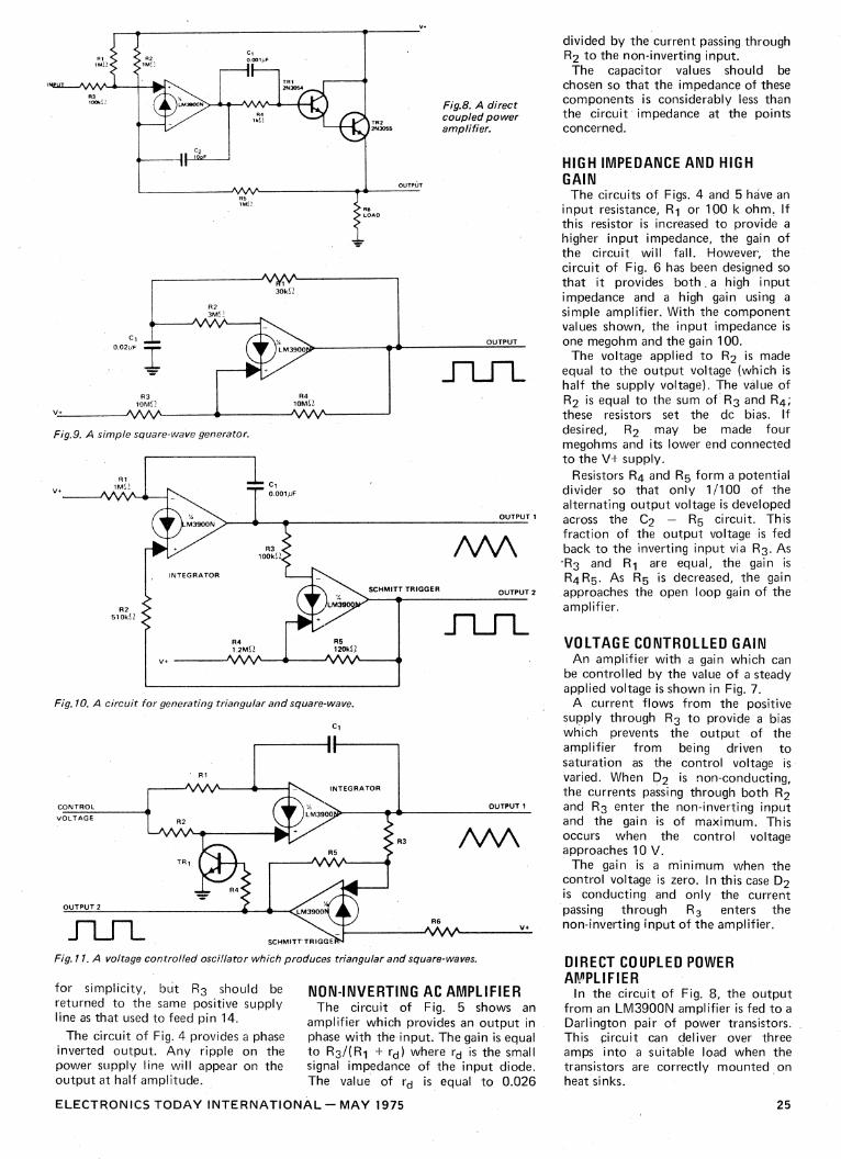
Fig.8. A direct coupled power amplifier.
V+
3OkS2
R2
R3 10MQ
1~-
LM3900 OUTPUT
Fig.9. A simple square-wave generator.
CONTROL o VOLTAGE
Fig. 10. A circuit for generating triangular and square-wave.
Cl
I I
R1
R2
R3
As/V5 TR.!
R6
SCHMITT TRIGGE
OUTPUT 1
INTEGRATOR
1/4 LM3900
OUTPUT 2
OUTPUT 1
NV\ INTEGRATOR
SCHMITT TRIGGER
R4 R5 1.2MS2 120W
V+ AAAA-0-MAA
OUTPUT 2
R1 MS2
V+ Ci
I0.00111F
R3 100kS2
R2 510kQ
Fig.11. A voltage controlled oscillator which produces triangular and square-waves.
for simplicity, bUt R3 should be returned to the same positive supply line as that used to feed pin 14.
The circuit of Fig. 4 provides a phase inverted output. Any ripple on the power supply line will appear on the output at half amplitude.
NON-INVERTING AC AMPLIFIER The circuit of Fig. 5 shows an
amplifier which provides an output in phase with the input. The gain is equal to R3/(R1 + rd) where rd is the small signal impedance of the input diode. The value of rd is equal to 0.026
divided by the current passing through R2 to the non-inverting input. The capacitor values should be
chosen so that the impedance of these components is considerably less than the circuit impedance at the points concerned.
HIGH IMPEDANCE AND HIGH GAIN
The circuits of Figs. 4 and 5 have an input resistance, R1 or 100 k ohm. If this resistor is increased to provide a higher input impedance, the gain of the circuit will fall. However, the circuit of Fig. 6 has been designed so that it provides both . a high input impedance and a high gain using a simple amplifier. With the component values shown, the input impedance is one megohm and the gain 100.
The voltage applied to R2 is made equal to the output voltage (which is half the supply voltage). The value of R2 is equal to the sum of R3 and R4; these resistors set the dc bias. If desired, R2 may be made four megohms and its lower end connected to the V+ supply.
Resistors R4 and R5 form a potential divider so that only 1/100 of the alternating output voltage is developed across the C2 — R5 circuit. This fraction of the output voltage is fed back to the inverting input via R3. As -R3 and R1 are equal, the gain is R4 R5. As R5 is decreased, the gain approaches the open loop gain of the amplifier.
VOLTAGE CONTROLLED GAIN An amplifier with a gain which can
be controlled by the value of a steady applied voltage is shown in Fig. 7.
A current flows from the positive supply through R3 to provide a bias which prevents the output of the amplifier from being driven to saturation as the control voltage is varied. When D2 is non-conducting, the currents passing through both R2 and R3 enter the non-inverting input and the gain is of maximum. This occurs when the control voltage approaches 10 V.
The gain is a minimum when the control voltage is zero. In this case D2 is conducting and only the current passing through R3 enters the non-inverting input of the amplifier.
DIRECT COUPLED POWER AMPLIFIER
In the circuit of Fig. 8, the output from an LM3900N amplifier is fed to a Darlington pair of power transistors. This circuit can deliver over three amps into a suitable load when the transistors are correctly mounted on heat sinks.
ELECTRONICS TODAY INTERNATIONAL — MAY 1975
25

INPUTS
Fig. 12. A voltage comparator with an indicator lamp.
R3 itwal2
INPUT (1)
V.-
Si
R7 10141
#V\AA
RS Isokit
C2 0.05pF INPUT (2)
R6 5.1MSZ
V+ AMPLIFIER
RI1 INAS/
AAAA
OUTPUT
R12 100k1/
C3 0.050
INPUT (3)
R9 100IcSZ
V+ 5.1mSi
R10
*WINNER 3
v+
S3
Fig.13. An audio mixer unit.
rig. 11. As in Fig.10, one amplifier is employed as an integrator.
When the output of the Schmitt trigger is high, the clamp transistor TR1 is conducting and the input current passing through R2 is shunted to ground. The current passing through R1 causes a falling ramp to be formed.
When the Schmitt circuit changes state, its output switches TRi to the non-conducting state. The current flowing through R2 can be made twice that flowing through R1 (R2 R1/2) so that the rising part of the ramp has a similar slope to the negative part.
The greater the value of the control voltage in Fig.11, the greater the frequency of oscillation. However, the voltage must exceed the constant input voltage (VBE ) or the circuit will fail to oscillate.
VOLTAGE COMPARATOR The circuit-of Fig. 12 shows how an
LM3900N amplifier may be employed to compare two input voltages and to indicate the result by means of a small lamp. If the input voltage connected to the non-inverting input is appreciably more positive than the other input, the output of the amplifier will provide a positive voltage which renders TR2 conducting. The lamp will then be illuminated.
One of the inputs may be a reference voltage so that one can then compare a single input voltage against this constant reference.
SQUAREWAVE GENERATOR The multiple amplifiers in the
LM3900N device are very suitable for use in waveform generators at frequencies of up to about 10 kHz. Voltage controlled oscillators (the frequency of which is dependent on an input voltage) can also be designed using the device.
A simple square wave generator is shown in Fig. 9. The capacitor C1 alternately charges and discharges between voltage limits which are set by R2 R3 and R4. The circuit is basically of the Schmitt trigger type,. the voltages at which triggering occurs being approximately V+/3 and 2V+/3.
TRIANGULAR WAVEFORM GENERATOR
A triangular waveform generator can be made by using one amplifier of a LM3900N device as an integrator and another amplifier as a Schmitt trigger circuit. A suitable circuit is shown in Fig. 10; it has the unusual advantage that only the one power supply is required.
When the output voltage from the Schmitt trigger circuit is low, the current flowing through R2 is integrated by C1 to produce the negative slope of the triangular wave at output 1. When the output 2 voltage from the Schmitt trigger is high, current flows through R2 to produce the rising part of the waveform at output 1.
The output waveform will have good symmetr9 if Ri = 2R2. The output frequency is given by the equation:
V+ VB E 2R1C1 V
where R1 - 2R2, VBE is the steady voltage at the inverting input (0.5 V) and V is the difference between the tripping points of the Schmitt trigger.
VOLTAGE CONTROLLED OSCILLATOR
A simple voltage controlled oscillator circuit which produces both triangular and square wave outputs is shown in
AUDIO MIXER The amplifiers of a LM3900N device
can be conveniently used to make a mixer unit for audio purposes; the unit enables three separate audio signals to be mixed together to produce a composite output. The circuit shown in Fig. 13 provides this facility using only a single LM3900N device and also enables any one channel to be selected be switches. The currents passing through the resistors R4 R8 and R12 are summed in the input circuit of the fourth amplifier.
If Si is open, amplifier 1 will be driven to saturation by the current passing through R2. It will therefore be inactive.
CONCLUSION This short article has attempted to
show a few of the numerous applications of this economical integrated circuit. Many more applications (such as phase locked
ternperature sensing circuits, tlifferentiators, tachometers, staircase generators, active filters, etc) are given in a report AN-72 produced by National Semiconductor. •
ELECTRONICS TODAY INTERNATIONAL. - MAY 1975
27
Fig 1 Z80 'add with carry' instruction
Fig 2 Z80 16-bit addition
Load D with first number: Load H. with second rume
Store (RESULT),:H:
Fig 3 Z80 alternative 16-bit addition
ASSEIV1131. This is part six of APC's Teach Yourself Assembler series. It's unique in using Basic as its point of reference, and avoiding the 'drop you in it' approach often used on this subject. Three pro-cessors, the Z80, 6502 and 8080 are covered in detail, but enough informa-tion is provided to enable users of other processors to follow the course. Copies of earlier articles in the series, which started in March 1984, may be obtained from our Back Issues dept.
Paul Overaa discusses the arithmetic operations of addition, subtraction, multiplication and division
on the 6502, Z80 and 8080 processors.
The basic arithmetic instructions avail-able on the 8080, Z80 and 6502 proces-sors are for addition and subtraction. The 6502 operates on 8-bit operands only, but both the 8080 and Z80 have certain instructions that enable 16-bit operands to be dealt with.
we can write A <--A + operand. Various forms of addressing are possible, as follows: ADDA,8: addsthe immediatevalue 8 to the accumulator — that is, is perform-ing the function A 4-- A + 8. ADD A,B: adds the contents of the B register to the accumulator, thus per-forming the function A A + B. ADD A,(HL): adds to the accumulator the contents of the byte whose address is specified by HL — that is, A A + (HL). ADD A,(IX+d): in the indexed addres-sing form, the address of the byte to be added is found by adding a specified displacement to the address held in index register IX. The symbolic repre-sentation is A A + (IX+d).
Instructions for 16-bit operations use HL, IX or IY as destination registers. Typical examples are as follows: ADD HL,DE; adds the contents of the DE pairto the contents of HL, thus perform-ing HL HL+DE. ADD IX,BC: in a similar fashion, this adds the contents of BC to the index register IX.
On the Z80, the instruction 'add with carry' (ADC) will include, in the 'addi- tion', the carry flag value: ADC A,B will perform the function A + B + Carry. The usefulness of this instruction can be seen from the example in Fig 1. We add two 'two byte numbers' — 255 and 257 — by adding the two low bytes first and then adding the two high bytes.
The addition ofthe low bytes causes a 'carry' to occur: the ADC instruction takes it into account when the high bytes are added. As a general rule, multibyte addition is performed by using a normal addition instruction for the first (least significant) bytes, and using the 'add with carry' instructions for succeeding bytes. The program in Fig 2 adds the contents of two 'two byte numbers' held in locations labelled FIRST$NUMBER and SECOND$-NUMBER.
Because of the existence of double register addition instructions, it's possible to write a much simpler 16-bit addition program onthe Z80. DE and Hi. can be loaded directly with the num- bers to add, and an ADD HL,DE instruction used to perform the 16-bit addition with one addition instruction (Fig 3).
Addition 8080 Immediate loading of 8080 register pairs uses a LXI instruction. LXI H, SECOND$NUMBER will load the HL pair with the 16-bit address equivalent to the label SECOND$NUMBER. LDA is a -direct loading of the accumulator from the byte whose address is FIRST$NUMBER. 'M' is the 8080 assembler convention to specify an
Addition Z80 On the Z80, addition instructions take the form ADD A, operand. The specified operand is addedtothevalue present in the accumulator, and in symbolic form
Page 110 Australian Personal Computer
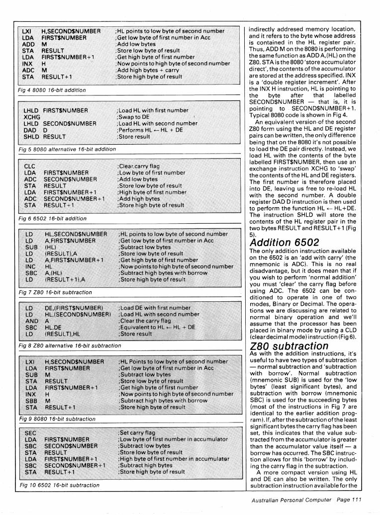
H SECOND$NUMBER FIRST$NUMBER M RESULT FIRST$NUMBER
M RESULT+
,HL poin s to low byte of second number Get low byte of first number in Acc Add low bytes
;Store low byte of result ;Get high byte of first number
'Now points to high byte of second flu ;Add high bytes + carry
ber
;Store high byte of result
LX LDA ADD STA LDA 1NX ADC STA
LHLD FIRST$NUMBER XCHG LHLD SECOND$'NUl1BER DAD D SHLD RESULT
Load H ;Swap to DE ,;I-bad HL with second nunlbe performs HL HL DE Store result
;Clear.carry ;Low byte of ;Add low bytes ;Store low byte of result ;High byte of first numbe .Add high bytes Store high byte of resul
FIRST$NUMBER SECONDSNUMBER
RESULT FIRST$NUMBER +1 SECONDSNUW1BER + RESULT+ 1
HL,SECONDSNUM ER A,FIRT$UMBER HL) RESULTY,A
A,FIRSTSNUivlBER HL A,(HL (RESULT 1),A
HL points tai low!Iff?1!•,:.,pipPliq44„, 90tio*Iotrog t ttlourob6IfttrAtt"' Subtract tioWilVtlet Store low byte of result het high byte of first number t ow po ntsto high byte of second nun bei Subtract Store hr h byte
result
LD L.() SUB
LD NC SBC
1411111(SECIONDSNUMBER) A
RESULT)
ad DE w.
Fig 4 8080 16 -bit addition
Fig 5 8080 alternative 16 -bit addition
Fig 6 6502 16 -bit addition
Fig 7 Z80 16 -bit subtraction
Fig 8 Z80 alternative 16-bit subtraction
RESULT F1RST$NU L A
INX H SBI3 M STA RESU T+
Fig 9 8080 16 -bit subtraction
SEC LDA $11Bp"
JiSTAI LDA SBC STA
F
RESULT
SECODNUMBER
et r ;Lo ;byte offirs 111:1401:00L rr accurlator ,,4011t41?ttittt*OYOL_ u
lt
,Store low byte of re; igb byte of first number n accumu ado,: ;Subtract high bytes "Stotditligk?OrOlotresult
Fig 10 6502 16 -bit subtraction
Let low oyte o' 4g .
Get high byteNow pontsto high byte
>>>>6.".. :rtyL ,efitt,Ilogroppor
ubtract high bytes with burro nr Store high byte of reesult
:ore
•
indirectly addresed memory location, and it refers to the byte whose address is contained in the HL register pair. Thus, ADD M on the 8080 is performing the same function as ADD A,(HL) on the Z80. STA is the 8080 'store accumulator direct', the contents of the accumulator are stored at the address specified. INX is a 'double register increment'. After the INX H instruction, HL is pointing to the byte after that labelled SECOND$NUMBER — that is, it is pointing to SECOND$NUMBER+1. Typical 8080 code is shown in Fig 4.
An equivalent version-of the second Z80 form using the HL and DE register pairs can be written, the only difference being that on the 8080 it's not possible to load the DE pair directly. Instead, we load HL with the contents of the byte labelled FIRST$NUMBER, then use an exchange instruction XCHG to 'swap' the contents of the HL and DE registers. The first number is therefore placed into DE, leaving us free to re-load HL with the second number. A double register DAD D instruction is then used to perform the function HL HL+DE. The instruction SHLD will store the contents of the HL register pair in the two bytes RESULT and RESULT+ 1 (Fig 5).
Addition 6502 The only addition instruction available on the 6502 is an 'add with carry' (the mnemonic is ADC). This is no real disadvantage, but it does mean that if you wish to perform 'normal addition' you must 'clear' the carry flag before using ADC. The 6502 can be con-ditioned to operate in one of two modes, Binary or Decimal. The opera-tions we are discussing are related to normal binary operation and we'll assume that the processor has been placed in binary mode by using a CLD (cleardecimal mode) instruction (Fig 6).
Z80 subtraction As with the addition instructions, it's useful to have two types of subtraction — normal subtraction and 'subtraction with borrow'. Normal subtraction (mnemonic SUB) is used for the low bytes' (least significant bytes), and subtraction with borrow (mnemonic SBC) is used for the succeeding bytes (most of the instructions in Fig 7 are identical to the earlier addition prog-ram). If, after the subtraction of the least significant bytes the carry flag has been set, this indicates that the value sub-tracted from the accumulator is greater than the accumulator value itself — a borrow has occurred. The SBC instruc-tion allows for this 'borrow' by includ-ing the carry flag in the subtraction.
A more compact version using HL and DE can also be written. The only subtraction instruction available forthe
Australian Personal Computer Page 111
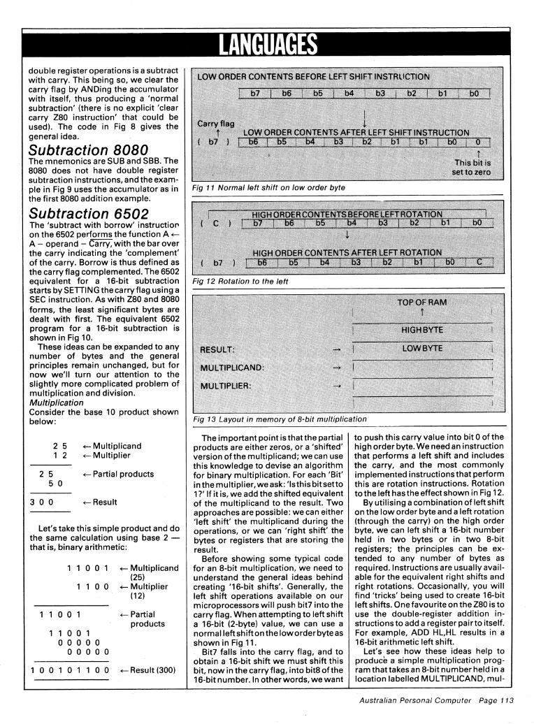
ESUPilligglit„,i.„„„„„„,„„„,„„„,
Fig 11 Normal left shift on low order byte
Fig 12 Rotation to the left
Fig 13 Layout in memory of 8 -bit multiplication
double register operations is a subtract with carry. This being so, we clear the carry flag by ANDing the accumulator with itself, thus producing a 'normal subtraction' (there is no explicit 'clear carry Z80 instruction' that could be used). The code in Fig 8 gives the general idea.
Subtraction 8080 The mnemonics are SUB and SBB. The 8080 does not have double register subtraction instructions, and the exam-ple in Fig 9 uses the accumulator as in the first 8080 addition example.
Subtraction 6502 The 'subtract with borrow' instruction on the 6502 performs the function AE-A — operand — Carry, with the bar over the carry indicating the 'complement' of the carry. Borrow is thus defined as the carry flag complemented. The 6502 equivalent for a 16-bit subtraction starts by SETTING the carry flag using a SEC instruction. As with Z80 and 8080 forms, the least significant bytes are dealt with first. The equivalent 6502 program for a 16-bit subtraction is shown in Fig 10.
These ideas can be expanded to any number of bytes and the general principles remain unchanged, but for now we'll turn our attention to the slightly more complicated problem of multiplication and division. Multiplication Consider the base 10 product shown below:
+-- Multiplicand Multiplier
2 5 Partial products 5 0
3 0 0 4— Result
Let's take this simple product and do the same calculation using base 2 -that is, binary arithmetic:
1 1 0 0 1 4— Multiplicand (25)
1 1 0 0 <— Multiplier (12)
4— Partial products
1 1 0 0 1 0 0 0 0 0
0 0 0 0 0
1 0 0 1 0 1 1 0 0 Result (300)
The important point is that the partial products are either zeros, or a 'shifted' version of the multiplicand; we can use this knowledge to devise an algorithm for binary multiplication. For each 'Bit' in the multiplier,we ask: 'Isthis bitsetto 1?' If it is, we add the shifted equivalent of the multiplicand to the result. Two approaches are possible: we can either 'left shift' the multiplicand during the operations, or we can 'right shift' the bytes or registers that are storing the result.
Before showing some typical code for an 8-bit multiplication, we need to understand the general ideas behind creating '16-bit shifts'. Generally, the left shift operations available on our microprocessors will push bit7 into the carry flag. When attempting to left shift a 16-bit (2-byte) value, we can use a normal left shift on the low order byte as shown in Fig 11.
Bit7 falls into the carry flag, and to obtain a 16-bit shift we must shift this bit, now in the carry flag, into bit8 of the 16-bit number. In other words, we want
to push this carry value into bit 0 of the high order byte. We need an instruction that performs a left shift and includes the carry, and the most commonly implemented instructions that perform this are rotation instructions. Rotation to the left has the effect shown in Fig 12.
By utilising a combination of left shift on the low order byte and a left rotation (through the carry) on the high order byte, we can left shift a 16-bit number held in two bytes or in two 8-bit registers; the principles can be ex-tended to any number of bytes as required. Instructions are usually avail-able for the equivalent right shifts and right rotations. Occasionally, you will find 'tricks' being used to create 16-bit left shifts. One favourite on the Z80 is to use the double-register addition in-structions to add a register pair to itself. For example, ADD HL,HL results in a 16-bit arithmetic left shift.
Let's see how these ideas help to produce a simple multiplication prog-ram that takes an 8-bit number held in a location labelled MULTIPLICAND, mul-
2 5 1 2
1 1 0 0 1
Australian Personal Computer Page 113
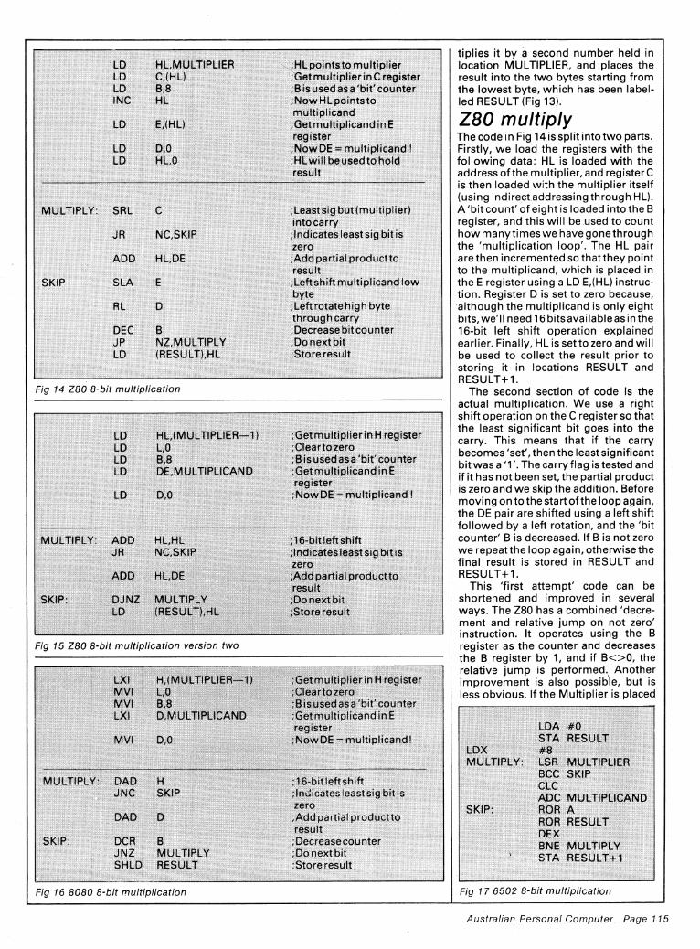
HL,MULTIPL..1E11 LD
C,(1-IL) LD
8,8 INC
HL
LD E,(HL)
LD D,0 LD 1.41,0
;HLpointsto multiplier ;Get multiplier in C register ;8 is used as a 'bit' counter ;Now HL points to multiplicand
; Get multiplicand in E register ; NOW DE multiplicand ! ;HL will beused to hold result
MULTIPLY: SRL C
JR
NC,SKIP
ADD HL,DE
SKIP
SLA
RL
DEC B JP N Z,IVIULTIf''LY
LD (RESULT),FiL
;Leastsig but (multiplier) intocarry ;Inclicatesleastsig bit is zero ;Add partial product to result ;Leftshift multiplicand low byte
; Left rotate high byte through carry ; Decrease bit counter ;Do next bit ;Store result
LD HL,(MULTIPI...IEF1--1 LD L,0 LD 8,8 LD DE,MULTIPLICAND
Itiplierin H register ;Getmu ;Clearto zero ;8 isusedasa 'bit' counter ;Get multiplicand in E register
;Now DE -- multiplicand!
SKIP:
JR
ADD
LD
HL,I-it..
HL,DE
MULTIPLY (F3ESULT),HL
;16-bit left shift ;Iridicatesleast sig bit is zero ,:Add partial procluctto result
;Done)(t bit ;Store result
LXI ) MVI L,0 MVI 8,8 La D,MULTIPLICAND
MVI D,0
;Getmultiplier in H register ; Clearto zero .B is used as a bit' counter ;Get multiplicand in register ;NovvDE ---- multiplicand!
SKIP:
TIPLY
DAD
D. B JNZ MULTIPLY sHLD RESULT
;16-bit left shift ;Indicates least sig bit is zero
;Add partial product to result ;Decreasecounter ;Do next bit ; Store result
LDA STA #8 LSRMULTIPLIER f3CC SKIP CLC ADC MULTIPLICAND ROR A ROR RESULT:: DEX BNE MULTIPLY STA RESULT+ 1
Fig 14 Z80 8-bit multiplication
Fig 15 Z80 8 -bit multiplication version two
tiplies it by a second number held in location MULTIPLIER, and places the result into the two bytes starting from the lowest byte, which has been label-led RESULT (Fig 13).
Z80 multiply The code in Fig 14 is split into two parts. Firstly, we load the registers with the following data: HL is loaded with the address of the multiplier, and register C is then loaded with the multiplier itself (using indirect addressing through HL). A 'bit count' of eight is loaded into the B register, and this will be .used to count how manytimeswe have gone through the 'multiplication loop'. The HL pair are then incremented so that they point to the multiplicand, which is placed in the E register using a LD E,(HL) instruc-tion. Register D is set to zero because, although the multiplicand is only eight bits, we'll need 16 bits available as in the 16-bit left shift operation explained earlier. Finally, HL is set to zero and will be used to collect the result prior to storing it in locations RESULT and RESULT+1.
The second section of code is the actual multiplication. We use a right shift operation on the C register so that the least significant bit goes into the carry. This means that if the carry becomes 'set', then the least significant bit was a 'V. The carry flag is tested and if it has not been set, the partial product is zero and we skip the addition. Before moving on to the start of the loop again, the DE pair are shifted using a left shift followed by a left rotation, and the 'bit counter' B is decreased. If B is not zero we repeat the loop again, otherwise the final result is stored in RESULT and RESULT+ 1.
This 'first attempt' code can be shortened and improved in several ways. The Z80 has a combined 'decre-ment and relative jump on not zero' instruction. It operates using the B register as the counter and decreases the B register by 1, and if B<>0, the relative jump is performed., Another improvement is also possible, but is less obvious. If the Multiplier is placed
Fig 17 6502 8-bit multiplication Fig 16 8080 8 -bit multiplication
Australian Personal Computer Page 115
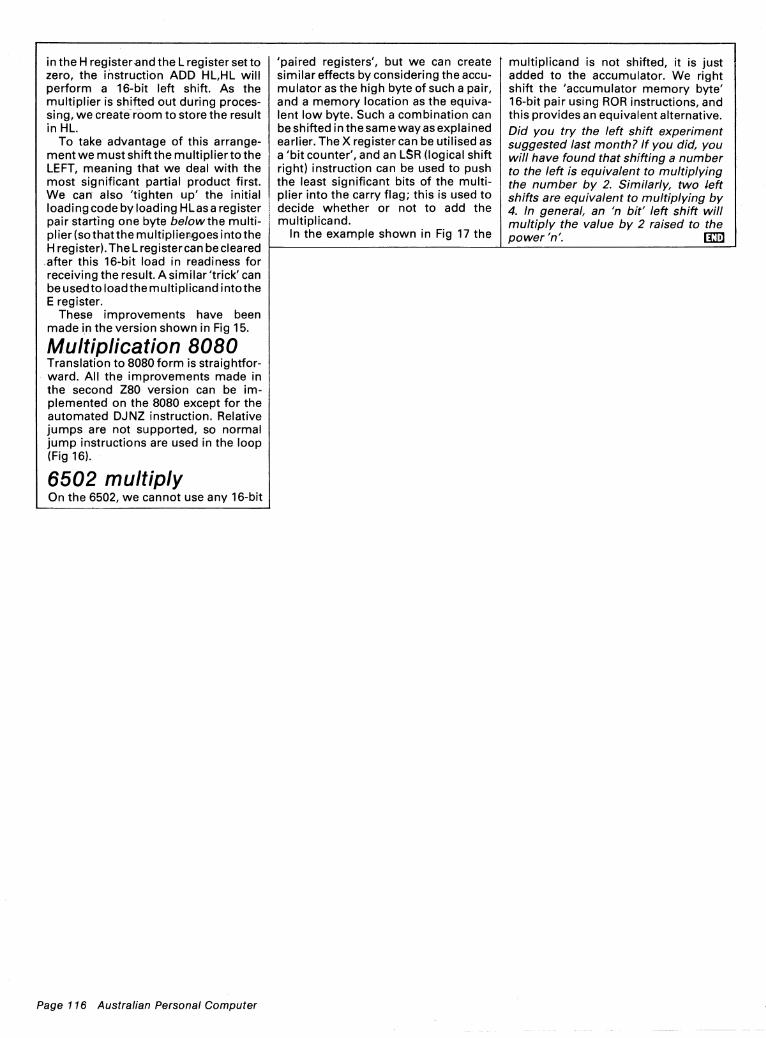
in the H registerand the L register set to zero, the instruction ADD HL,HL will perform a 16-bit left shift. As the multiplier is shifted out during proces-sing, we create room to store the result in HL.
To take advantage of this arrange-ment we must shift the multiplier to the LEFT, meaning that we deal with the most significant partial product first. We can also 'tighten up' the initial loading code by loading HL as a register pair starting one byte below the multi-plier (so that the multipliervoes into the H register). The L register can be cleared .after this 16-bit load in readiness for receiving the result. A similar 'trick' can be used to load the multiplicand into the E register.
These improvements have been made in the version shown in Fig 15.
Multiplication 8080 Translation to 8080 form is straightfor-ward. All the improvements made in the second Z80 version can be im-plemented on the 8080 except for the automated DJNZ instruction. Relative jumps are not supported, so normal jump instructions are used in the loop (Fig 16).
'paired registers', but we can create similar effects by considering the accu-mulator as the high byte of such a pair, and a memory location as the equiva-lent low byte. Such a combination can be shifted in the same way as explained earlier. The X register can be utilised as a 'bit counter', and an LSR (logical shift right) instruction can be used to push the least significant bits of the multi-plier into the carry flag; this is used to decide whether or not to add the multiplicand.
In the example shown in Fig 17 the
multiplicand is not shifted, it is just added to the accumulator. We right shift the 'accumulator memory byte' 16-bit pair using ROR instructions, and this provides an equivalent alternative. Did you try the left shift experiment suggested last month? If you did, you will have found that shifting a number to the left is equivalent to multiplying the number by 2. Similarly, two left shifts are equivalent to multiplying by 4. In general, an 'n bit' left shift will multiply the value by 2 raised to the
6502 multiply On the 6502, we cannot use any 16-bit
Page 116 Australian Personal Computer

18 11 A7 23 ED 42 E5 EEI 19 EB 09 EB ED 42 50 59 E3 Cl Of3 2B E5 D5 C5 62 6B 1A 38 05 23 ED BC 18 03 28 ED B8 12 Cl Di Ei F5 7C B5 28 03 Fl 18 E3 Fl C9
;restore flags ;and continue ;restore to and return
APC SUBSET Alan Tootill and David Barrow present more useful assembler language subroutines. This is your chance to build a library of general-purpose routines, documented to the standard we have developed together in this series. You
can contribute a Datasheet, improve or develop one already printed or translate the implementation of a good
idea from one processor to another. APC will pay for those contributions that achieve Datasheet status. Contributions (for
any of the popular processsors) should be sent to 3UB SET, 77 Glenhuntly Road, Elwood, Vic 3184.
Z80 block relocation Several of you liked R Cath's 6502 block relocation routine RRL (misprinted as 6802 Block relocation, November '83) well enough to implement it for other processors. First, a couple of errors. LDA M9 should be
inserted at the 1 7th. instruc-tion. The 41st. instruction should have been BBCRRL3. We apologise to the BBC.
For the Z80, we like this effort from Mark Wenham. His ROLR moves a block to either a lower or higher memory address using the Z80 block move instruc-tions. One of its best features is its simple, unambiguous input require-
ments; the address of the first byte to be moved, the address of the last byte to be moved and the address to which the block is to be moved. Where the block is moved to a higher memory
address, memory below the destination is moved down to make way for it and where the block is moved to a lower memory address, memory above the destina-tion is moved up.
Australian Personal Computer Page 145

HIRES SCREEN DUMPS FOR 1520 PLOTTER Hires screen dumps are possible on a 1520 plotter,
with this routine, using a VIC 20 and super expander. It should also work with a Commodore 64 and Simon's Basic if it has the RDOT function or something similar to test whether a point is on or off. S Mills
nellitREITURN
BACKGROUND VZ One of the limitations of the VZ-200 is that it has only two background colours in each mode: green and orange in mode 0, buff and green in mode 1. This short machine code program fills the screen with any desired character in either mode 0 or 1, making any of the eight foreground colours available as a background.
To use the program just
Basic listing:
type in the listing, either at the start of another program or on its own, and CSAVE it. RUN the program and, to fill the screen, POKE the code for the desired character into location 28672 (start of screen address) and enter PRINT USR(0). In mode 1 and colour 0, 0 gives a green background, 85 gives yellow, 170 blue and 255 gives a red background. In mode 1, colour 1, buff = 0, cyan = 85, 170 = orange and 255 = magenta.
I Williams
Page 110 Australian Personal Computer
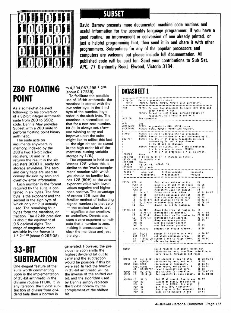
DATASHEET 1 FETCH
40FUF
•
:ACTION
Fetch arguments to stack. (MOPDZ, MOPNR, MOPOV, MOPUF) Exit correctly. ==.2:.=======.===...mms==sza======s ,....smica,:zr===== FETCH: To copy two arguments to stack work area and
clear result flags. MOPUP: To set correct flags, zeroise result if
necessary, pull results and exit. See comments.
:CPAJ
:HARDWARE :SOFTWARE
:INPUT
:OUTPUT
:ERRORS :REG USE :STACK USE :RAM USE :LENGTH :CYCLES
Z80 FETCH: arguments in RAM. MOFUP: none. FETCH: none. MOPUP: "NORM" and "ROUND".
FETCH: IX ind IY address the two arguments MOPUP: Result in .,-bytes on sack addressed by IX. FETCH: IX, IY, on stack. Arguments on stack
indexed by IX. All flags cleared. A, B, DE and HL changed.
MOPUP: Result in BCDEHL. IX, IY and A restored. Z = 1: division by zero (FPDIV). Z = 0: C = 1: overflow. C = 0: no error.
None. F BC DE HL IX IV (A changed in FETCH). 16 (MOPUF: -16), None. FETCH: 48. MOPUF: 39. Not given.
:CLASS 2' -discreet *interruptable *promable -Calif: 'reentrant *relocatable *robust -smss.rnsimszas...s..caz=aixxxxxsz
FETCH POP HL :Get return address in HL. El PUSH IX ;Save IX, IV and AF on stack DD ED PUSH IY :before stacked numbers, other FD E5 PUSH AF :registers used for output. F5 LD IX,-12 :Index stack area below DD 21 F4 FF ADD IX,SP :12-byte workspace and set DD 39 LD SP,IX :Stack pointer accordingly. DD F9 LD D,(IX+17) :Get stacked IX to DE for DO 56 11 LD E,(IX+16) :transfer loop source. DD 5E 10 LD 8,6 :Count for 6-byte numbers. 06 06
FETCHL LD A,(DE) :Move byte from 1st lumber to IA LD (IX+0),A :workspace low address. DD 77 00 LD A,(IY+0) :Move byte from 2nd number to FD 7E 00 LD (IX+6),A :workspace high address. DD 77 06 INC IX :Bump workspace pointer DD 23 INC DE and 1st number pointer 13 INC IY and 2nd number pointer. FD 23
DJN1 FETCHL :Repeat for 6-byte numbers. 10 EF •
LD DE,-6 :Reset IX to point to start 11 FA FF ADD IX,DE :of stack workspace area. DD 19 LD (IX+12),8 :Clear Z and Cy flags (0=0). DD 70 0C JP (HL) :Return by jumping. E9.
SET 6,(IX+12)
JR MOPPOP CALL NORM CALL ROOD
JR NZ,MOPPOP MOPOV SET 0,(IX+12) MOPUF LD (IX+0),0
MOPPOP LD SP,IX POP BC POP HL POP DE POP IX POP IX
:Set stacked Z flag to show :division by zero, and exit. :Normalise if necessary, :then round, and go exit if :result exponent not zero. :Set stacked Cy: overflow :Set exponent 0, zero result.
:Set SP at result, losing any :values on stack, and pick up :result in BCDEHL, B = sign, :C = exp, DEHL = mantissa. :Pop 6 bytes of 2nd argument into IX to discard it and
DD CB OC FL 18 10 CD lo hi CD lo hi 20 08 DD CB OC C6 DD 36 00 02
DD F9 Cl El D1 DD El DD El
MOPUP
MOPDZ
MOPNR
:Exit routine with entry points for :division by zero, overflow, underflow or :zero result, normalise and round.
David Barrow presents more documented machine code routines and useful information for the assembly language programmer. If you have a good routine, an improvement or conversion of one already printed, or just a helpful programming hint, then send it in and share it with other programmers. Subroutines for any of the popular processors and computers are welcome but please include full documentation. All published code will be paid for. Send your contributions to Sub Set, APC, 77 Glenhuntly Road, Elwood, Victoria 3184.
Z80 FLOATING POINT As a somewhat' delayed follow-up to his conversion of a 32-bit integer arithmetic suite from Z80 to 6502 code, Dennis May provides Subset with a Z80 suite to perform floating point binary arithmetic.
The suite acts on arguments anywhere in memory, indexed by the Z80's two 16-bit index registers, IX and IV. It returns the result in the six registers BCDEHL, ready for storage anywhere. The zero and carry flags are used to convey division by zero and overflow error information.
Each number in the format required by the suite is con-tained in six bytes. The first byte is the exponent and the second is the sign byte of which only bit 7 is actually used. The remaining four bytes form the mantissa, or fraction. The 32-bit precision is about the equivalent of 9.5 decimal digits. The range of magnitude made available by the format is 1 * 2-128 (about 0.29E-38)
33-BIT SUBTRACTION One elegant feature of the suite worth commenting upon is the implementation of 33-bit arithmetic in the division routine FPDIV. If, in any iteration, the 32-bit sub-traction of divisor from divi-dend fails then a borrow is
to 4,294,967,295 * 2 95 (about 0.17E39).
To facilitate the possible use of 16-bit arithmetic, the mantissa is stored with the low-order byte in the third byte of the number, high order in the sixth byte. The mantissa is normalised so that for a non-zero number, bit 31 is always set. (Any-one wishing to try and improve upon the suite might like to utilise this fact — the sign bit can be stored in the high order bit of the mantissa, cutting variable storage by 1/6.)
The exponent is held as an 'excess 128' value; this is similar to the 'two's comple-ment' notation with which you should be familiar but has 128 (80H) as the zero exponent value with lower values negative and higher ones positive. The advantage of excess 128 over the familiar method of indicating signed numbers is that zero — the easiest value to test — signifies either overflow or underflow. Dennis also uses a zero exponent to indi-cate that a number is zero, making it unnecessary to clear the mantissa and rest the sign.
generated. However, the pre-vious iteration shifts the highest dividend bit out to carry and the subtraction would be possible if this bit were set. In fact the borrow in 33-bit arithmetic will be the inverse of the shifted out bit, and the algorithm used by Dennis simply replaces the 32-bit borrow by the complement of the shifted bit.
Australian Personal Computer Page 165
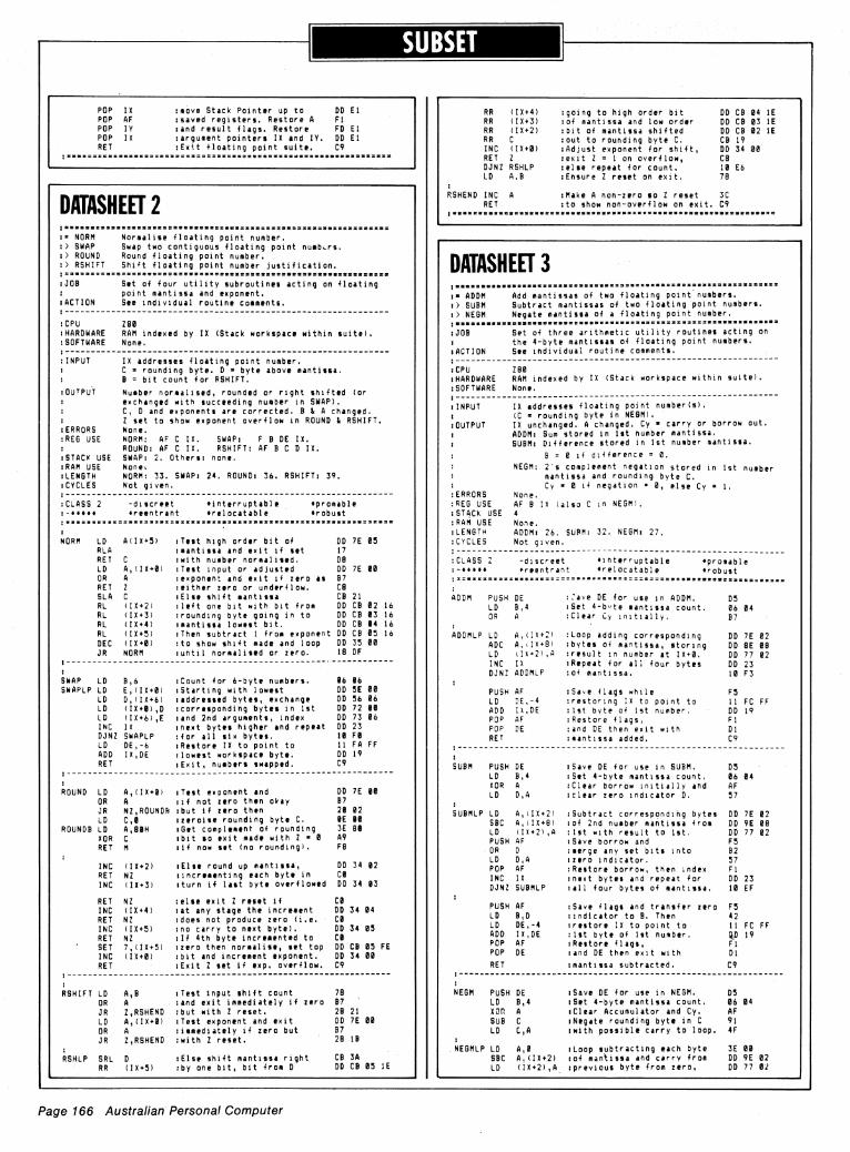
DATASHEET 2 ===== CL.272....C.X.X========XU=.1.1121.121==le===i===i===.1===i==iCin=
I. NORM Normalise floating point number. :> SWAP Swap two contiguous floating point numb,rs. 1> ROUND Round floating point number. :> RSHIFT Shift floating point number justification.
...... ............=======*.==========i==SX=====.=====!===
:JOB Set of four utility subroutines acting on floating point mantissa and exponent.
'ACTION See individual routine comments.
:CPU 280 :HARDWARE RAM indexed by IX (Stack workspace within suite). :SOFTWARE None.
:INPUT IX addresses floating point number. C = rounding byte. D = byte above mantissa. B = bit count for RSHIFT.
:OUTPUT Number normalised, rounded or right shifted (or exchanged with succeeding number in SWAP).
• C, D and exponents are corrected. B & A changed. Z set to show exponent overflow in ROUND & RSHIFT.
:ERRORS None. :REG USE NORM: AF C IX. SWAP: F B DE IX.
ROUND: AF C IX. RSHIFT: AF 8 C D IX. :STACK USE SWAP: 2. Others: none. :RAM USE None,, :LENGTH NORM: 33. SWAP: 24. ROUNDS 36. RSHIFT: 39. !CYCLES Not given.
:CLASS 2 -discreet *reentrant
: nag= ...... ==.1112=1121112.111
NORM
*interruptable *relocatable
*promable *robust
LD A(IX+5) 'Test high order bit of DD 7E 05 RLA !mantissa and exit if set 17 RET C with number normalised. D8 LD A,(IX+0) :Test input or adjusted DD 7E 00 OR A !exponent and exit if zero as B7 RET Z 'either zero or underflow. C8 SLA C 'Else shift mantissa CB 21 RL (10+2) :left one bit with bit from DO CB 02 16 RL (IX+3) :rounding byte going in to DD CB 03 16 RL (IX+4) *mantissa lowest bit. DD CB 04 16 RL (IX+5) !Then subtract 1 from exponent DD CB 05 16 DEC (11+0) :to show shift made and loop DD 35 00 JR NORM :until normalised or zero. 18 DF
SWAP LD 8,6 'Count for 6-byte numbers. 06 06 SWAPLP LD E,(I1+0) :Starting with lowest DD 5E 00
LD D,(IX+6) !addressed bytes, exchange DO 56 06 LD (I1+0),5 :corresponding bytes in 1st DD 72 00 LD (IX+6),E land 2nd arguments, index DD 73 06 INC IX 'next bytes higher and repeat DD 23 DJNZ SWAPLP for all six bytes. 10 PO LD DE,-6 !Restore IX to point to 11 FA FF ADD IX,DE slowest workspace byte. DD 19 RET :Exit, numbers swapped. C9
ROUND LD A,(IX+0) !Test exponent and DD 7E 00 OR A !if not zero then okay 87 JR NZ,ROUNDR but if zero then 20 02 LD CO, tzeroise rounding byte C. OE BO
ROUNDS LD A,80H 'Get complement of rounding 3E BO XOR C alit so exit made with Z ■ 0 A9 RET M !if now set (no rounding). F8
INC (IX+2) 'Else round up mantissa, DD 34 02 RET NZ :incrementing each byte in CO INC (11+3) :turn if last byte overflowed DD 34 03
RET NZ :else exit Z reset if CO INC (IX+4) at any stage the increment DD 34 04 RET NZ (does not produce zero (i.e. - CO INC (IX+5) no carry to next byte). DD 34 05 RET NZ If 4th byte incremented to CO
• SET 7,(IX+5) :zero then normalise, set top DD CB 05 FE INC (IX+0) :bit and increment exponent. DD 34 00 RET :Exit Z set if exp. overflow. C9
RSHIFT LD A,B 'Test input shift count 78 OR A . :and exit immediately if zero B7 JR Z,RSHEND but with Z reset. 2B 21 LD A,(IX+0) :Test exponent and exit DD 7E 00 OR A :immediately if zero but B7 JR Z,RSHEND with Z reset. 28 10
RSHLP SRL D :Else shift mantissa right CB 3A
RR (IX+5) by one bit, bit from D DD CO 05 lE
DATASHEET 3 Iscomman UUUUUU astanwammacumszassammess.nums.seman.s.m7sasmassm====. 1...
ADDM Add mantissas of two floating point numbers.
SUBM Subtract mantissas of two floating point numbers.
I> NEGM Negate mantissa of a floating point number. UUUUUUUUU Mili=211.1.11=MENUO.=12..Q....Ma=====U=======X= UUUU
:JOB Set of three arithmetic utility routines acting on the 4-byte mantissas of floating point numbers.
'ACTION See individual routine comments.
:CPU Z80 :HARDWARE RAM indexed by IX (Stack workspace within suite). :SOFTWARE None.
:INPUT IX addresses floating point number(s). (C = rounding byte in NEGM).
:OUTPUT IX unchanged. A changed. Cy = carry or borrow out. ADDM: Sum stored in 1st number mantissa. SUBM: Difference stored in 1st number mantissa.
B = 0 if difference = 0.
NEGM: 2's complement negation stored in 1st number mantissa and rounding byte C. Cy = 0 if negation = 0, else Cy = 1.
:ERRORS None. :REG USE AF B IX (also C in NEGM). :STACK USE 4 :RAM USE None. :LENGTH ADDM: 26. SUPM: 32. NEGM: 27. :CYCLES Not given.
------------------------- :CLASS 2 -discreet *interruptable *promable :-***** *reentrant *relocatable *robust
:S.UXX.SX==.111113.31C
ADDM PUSH DE ::ave DE for use in ADDM. D5 LD 8,4 :Set 4-b.te mantissa count. 06 04 OR A :Clear Cy initially. 07
ADDMLP LD A,(IX+2) :Loop adding corresponding DD 7E 02 ADC A,(IX+8) :bytes of mantissa, storing DD BE 08 LD (IX+2),A :result in number at IX+0. DD 77 02 INC IX :Repeat for all four bytes DD 23 DJNZ ADDMLP of mantissa. 10 F3
PUSH AF :Save flags while F5 LD DE,-4 :restoring IX to point to 11 FC FF ADD IX,DE :1st byte of 1st number. • DD 19 POP AF :Restore flags, Fl POP DE and DE then exit with DI RET :mantissa added. C9
SUBM PUSH DE :Save DE for use in SUBM. D5 LD 0,4 :Set 4-byte mantissa count. 06 04 XOR A :Clear borrow initially and AF LD D,A :clear zero indicator D. 57
SUBMLP LD A,(IX+2) :Subtract correspdndihg bytes DD 7E 02 SBC AOIX+8) of 2nd number mantissa from DD 9E 08 LD (lx+2),A :1st with result to 1st. DD 77 02 PUSH AF :Save borrow and F5
-OR D :merge any set bits into 02 LD D,A :zero indicator. 57 POP AF :Restore borrow, then index Fl INC IX :next bytes and repeat for DD 23 DJNZ SUBMLP tall four bytes of mantissa. 10 EF
PUSH AF :Save flags and transfer zero F5 LD B,D !indicator to 8. Then 42 LD DE,-4 !restore IX to point to 11 FC FF ADD IX,DE :1st byte of 1st number. p 19 POP AF :Restore flags, Fl POP DE and DE then exit with DI
RET :mantissa subtracted. C9
NEGM PUSH DE :Save DE for use in NEGM. D5 LD 0,4 :Set 4-byte mantissa count. 06 04 XOR A 'Clear Accumulator and Cy. AF SUB C 'Negate rounding byte in C 91 LD C,A with possible carry to loop. 4F
NEGMLP LD A,0 !Loop subtracting each byte SBC A,(IX+2) of mantissa and carry from LD (IX+2),A :previous byte from zero,
3E 00 DD. 9E 02 DD 77 02
RR (IX+4) :going to high order bit DD CB 04 lE RR (IX+3) of mantissa and low order DD CB 03 lE RR (IX+2) :bit of mantissa shifted DD CO 02 1E RR C out to rounding byte C. CB 19 INC (IX+0) :Adjust exponent for shift, DD 34 00 RET Z :exit Z = 1 on overflow, C8 DJNZ RSHLP :else repeat for count. 10 E6 LD A,B :Ensure Z reset on exit. 78
RSHEND INC A :Make A non-zero so Z reset 3C RET to show non-overflow on exit. C9
UUUUUUUUUU UUUUUUUU UUUUUUUU 127.W.UM2.2..MUMU.. UUUUU 11.111.11.111=0.111.1112.
POP IX :move Stack Pointer up to DD El POP AF :saved registers. Restore A Fl POP IY and result flags. Restore FD El POP IX :argument pointers IX and IY. DD El RET :Exit floating point suite. C9
Page 166 Australian Personal Computer
DATASHEET 4 /..1=2271.1. UUUUUUUUUUU E.Z=M=.1.11 UUUUU .. 2 1.7.11=MUMUMEMR.7111111111211.11.11.1.MOU
:= FPSUB Floating point subtraction. :> FPADD Floating point addition. 1== == ==ii..1.......C.M.2.111.111= = .11111:=XXIIII2.11....X.AMO MMX.0421.111 11.11111
:JOB
:ACTION
To perform addition or subtraction on two floating point numbers held in memory, returning a valid result in registers or error information in flags. Move numbers to stack workspace. IF either number = 0 THEN: C Return other number.] Equalise exponents, justifying mantissas. Add/subtract , mantissas with any necessary negation, justification, sign change or exponent zeroising. Exit, result to registers, setting correct flags.
:CPU :HARDWARE :SOFTWARE
:INPUT :OUTPUT
:ERRORS :REG USE :STACK USE :RAM USE :LENGTH :CYCLES
Z80 Memory containing the two numbers. FETCH MOPUP SWAP RSHIFT ADDM SUBM NEGM
IX addresses 1st number, IY 2nd number in memory. IX, IY and indexed numbers unchanged. Z a 0. Cy = 0: Result in BCDEHL. Cy a It Overflow. None. F BC DE HL IX IY 22 None. 95 Not given.
:CLASS 2 1-steetie
-discreet *reentrant
*interruptable *relocatable
*promable *robust
=it
FPADD CALL FETCH JR FPAS
:Move arguments to workspace CD lo hi on stack. Go to common part. 18 OB
FPSUB CALL FETCH
:Set arguments to workspace
CD lo hi LD A,-1
:and negate sign of second
3E FF XOR (11+7)
!number so add/sub operation
DD AE 07 LD (IX+7),A :is essentially the same. DD 77 07
FPAS LD OR CALL LD OR JP
SUB JR NEG CALL
FPASEQ LD LD LO CALL
A,(IX+0) A Z,SWAP A,(11+6) A Z,MOPPOP
(IX+O) NC,FPASEQ
SWAP C,0 D,C B,A RSHIFT
:Get and test 1st exponent for number = O. If so, move
:2nd number to result place. :Get and test 2nd exponent. :If zero, return 1st number as sum or difference.
:Subtract exponents to give :shifts needed to equalise :exponents, swapping numbers if necessary.
:Clear rounding byte and 'shift-in byte. :Move shift count to I and 'shift if needed.
DD 7E 00 B7 CC lo hi DD 7E 06 B7 CA lo hi
DD 96 00 30 05 ED 44 CD lo hi OE 00 51 47 CD lo hi
LD
A,(IX+1) :Compare signs. If same then
DD 7E 01 XOR
(IX.7) 'addition of mantissas is
DD AE 07 RLA
:needed but subtraction if
17 JR
C,FPMSUB 'signs are different. 38 10
CALL LD LD CALL JP JP
FPMSUB CALL PUSH LD OR JP POP CALL RRA XOR LD JP
ADDM B,1
C,RSHIFT Z,MOPOV MOPNR
SUBM AF A,B A Z,MOPUF AF C,NEGM
(IX+1) (IX+1),A MOPNR
:Add mantissas. Prepare for :shifting carry out of add :back into mantissa. :Shift any carry back in. :Exit if exponent overflow. :Normalise, round & exit.
:Subtract mantissas and, 'saving borrow, test if difference is zero,
:if so then exit clearing 'exponent to show number a 0. :restore borrow and negate :result if borrow generated. Use borrow to set correct
'result sign, negating sign only it Cy was set.
*Normalise, round & exit.
CD lo hi 06 01 16 01 DC lo hi CA lo hi C3 lo hi
CD lo hi F5 78 87 CA lo hi Fl DC lo hi IF DD AE 01 DD 77 01 C3 lo hi
INC IX :2's complement result back DD 23 DJNZ NEGMLP to number at IX+0. 10 F4
PUSH AF :Save flags while F5 LD DE,-4 :restoring IX to point to 11 FC FF ADD IX,DE :1st byte of 1st number. DD 19 POP AF :Restore flags, Fl POP DE and DE then exit with DI RET :mantissa negated. C9
Is ZZZZZZZZZZ sumucruss UUUUU Eammussaus===xsummimmum..smsammmuss
Australian Personal Computer Page 167

DATASHEET 5 : =XXXXIXXIM=XX ZZZZZ ZZZZZZZZ XXXXXXXXIXICSOW2XXXXX ZZZZZ =MUSE ZZZZZ ==
:= FPMUL Floating point multiplication. :=================sassss==emssmsss=ssssssssssss=a=ss=s=ss=ssssss
:JOB To perform multiplication on two floating point numbers held in memory, returning a valid product in registers or error information in flags.
:ACTION Move numbers to stack workspace. IF either number ■ 0 THEN: [ Return zero.] Add exponents, exiting on overflow or underflow.
: Product sign multiplier XOR multiplicand signs. Multiply mantissas. Normalise, round and exit, product to registers.
:CPU Z80 :HARDWARE Memory containing the two numbers. :SOFTWARE FETCH MOPUP ADDM
:INPUT IX addresses multiplier, IY multiplicand in memory. :OUTPUT IX, IY and indexed numbers unchanged. Z 0.
Cy = 0: Result in BCDEHL. Cy . 1: Overflow. :ERRORS None. :REG USE F BC DE HL IX IY :STACK USE 24 :RAM USE None. :LENGTH 110 :CYCLES Not given.
:CLASS 2 -discreet *interruptable *promable :-****e *reentrant *relocatable *robust
................... == ...... =========== ...... =====
FPMUL CALL FETCH
LD A,(IX+0) OR A
JP Z,MOPPOP
LD A,(IX+6) OR A
JP Z,MOPUF
ADD A,(IX+0) JR C,FPMPOS
JP P,MOPUF JR FPMEXS
FPMPOS JP M,MOPOV FPMEXS ADD A,80H
LD (IX+0),A
LD A,(1X+1) XOR (IX+7)
LD (IX+1),A
LD L,(IX+2) LD HOIX+3) PUSH HL
LD L,(IX+4) LD HOIX+5)
LD CO,
LD (IX+2),C
LD (IX+3),C
LD (IX+4),C
LD (IX+5),C
LD D,32
FPMLP SRL H RR L
EX (SP) ,HL RR H RR L
EX (SP),HL CALL C,ADDM
RR (IX+5)
RR (10+4)
RR (10+3)
RR (10+2) RR C
:Move numbers to workspace on :stack and test exponent of :multiplier, returning it as :product if zero. :Test multiplicand exponent :and exit with zero product :if it is zero.
:Else add exponents, use Cy :and S to determine if add :gives underflow or overflow and if so, exit with correct
:zero result/overflow flag. :Restore excess 128 exponent :to product exponent byte.
:Exclusive-OR multiplier and multiplicand signs to
:give product sign.
:Move multiplier mantissa :low-word to (SP) land high-word to HL for shifting in
:multiplication loop.
:Zeroise rounding byte :and product accumulator :(replacing multiplier :in workspace).
:Set 32 bit count.
:Long multiplication by shift :and addition at correct bit :place if multiplier bit set. :Shift right next multiplier :bit through HL and (SP) :intc Cy. :If set, add multiplicand and shift partial product
:right to next bit place, :getting any carry from :addition. Rounding byte :takes shift out bits.
CD lo hi DD 7E 00 B7 CA lo hi DD 7E 86 87 CA lo hi
DD 86 00 38 05 F2 lo hi 18 03 FA lo hi C6 88 DD 77 00
DD 7E 01 DD AE 07 DO 77 81
DD 6E 02 DD 66 83 ES DD 6E 84 DD 66 05
OE 88 DO 71 02 DD 71 83 DD 71 84 DO 71 05
16 20
C8 3C CB ID E3 CB 1C CB ID E3 DC lo hi DD CB 05 1E DD CB 04 1E DD CB 03 lE DD CB 82 lE CB 19
DEC D :Repeat for all 32 bits of 15 JR NZ,FPMLP :multiplier. DO DE JP MOPNR :Normalise, round & exit. C3 lo hi
: XXXUSUXXXIXX==1111.1=XXEM .....
Subtract exponents, exit on overflow or underflow. Quotient sign = dividend XOR divisor signs. Divide mantissas. Normalise, round and exit, quotient to registers.
:CPU Z80 :HARDWARE Memory containing the two numbers. :SOFTWARE FETCH MOPUP SUBM ADDM
:INPUT IX addresses dividend, IY divisor in memory. :OUTPUT IX, IY and indexed numbers unchanged.
:ERRORS :REG USE :STACK USE :RAM USE :LENGTH :CYCLES
Z = 1: division by zero. 0: Cy . 0: Result in BCDEHL. Cy = 1: Overflow.
None. F BC DE HL IX IY 24 None. 114 Not given.
-discreet *interruptable *promable *reentrant *relocatable *robust
2. XXXXX.X.E=XXXS.XXXXXXXXX==2========g===ii.TX
:CLASS 2 :-***** !XX7112=X
'In my day, Mr Hobson, we used to throw chalk at them!'
FPDIV CALL LD OR JP LD OR JP
SUB . JR
JP JR
FPDPOS JP FPDEXS ADD
JP LD
LD A,(IX+1) XOR (IX+7) LD (IX+1),A LD HL,0 PUSH HL LD C,H LD D,34
FPDLP RL E CALL SUBM JR NC,FPDAD RR E CCF
FPDAD CALL C,ADDM JR C,FPDRS SET 5,C
FPDRS SLA C ADC HL,HL EX (SP),HL ADC HL,HL EX (SP),HL SLA (IX+2) RL (IX+3)
RL (18+4) RL (10+5) DEC D JR NZ,FPDLP
LD (IX+2),L LD (IX+3),H POP HL LD (IX+4),L LD (IX+5),H JP MOPNR
FETCH A,(IX+6) A Z,MOPDZ A,(IX+0) A Z,MOPUF
(IX+6) :Subtract exponents, use Cy NC,FPDPOS and S to test if subtraction P,MOPUF :gives underflow/overflow, FPDEXS if so exit with correct M,MOPOV :zero quotient/overflow flag. A,81H :Correct excess 128 exponent Z,MOPOV :+1 for bit normalisation, (IX+0),A :exiting if overflow.
:Shift partial quotient and :rounding byte in :(SP), HL and C one bit left :to next bit place.
:Shift dividend left by one bit to next bit place
:top bit out to Cy. :Repeat for 34 bits :needed to ensure correct :normalised, rounded quotient.
:Move quotient mantissa :from (SP) and HL to :replace dividend in stack :workspace as raw quotient :then exit to normalise and round.
:Move numbers to workspace on :stack and test exponent of :divisor. If zero then error :exit - division by zero. :Test dividend exponent, if :zero then return valid :zero quotient.
:Exclusive-OR dividend and DD :divisor sign to give quotient DD :sign, replacing dividend. DD :Clear quotient mantissa in 21 :(SP) and HL, clear rounding E5 :byte C. Set D as 32-bit count 4C :+ 1 normalisation + 1 round. 16 22
:Save hi-bit shifted out of CB :dividend and subtract divisor CD :skip if subtraction went ok 30 :else correct for 33-bit CB :subtraction. If still no go 3F :then add divisor back and DC :skip quotient bit setting. 38 :Set correct place bit. CB
DD 75 02 DO 74 03 El DD 75 84 DD 74 05 C3 lo hi
DD CB 84 16 DD CB 85 16 15 28 D4
CB 21 ED 6A E3 ED 6A E3 DO CB 02 26 DD CB 03 16
CD lo hi DD 7E 06 B7 CA lo hi DD 7E 08 87 CA lo hi
DO 96 06 30 85 F2 lo hi 18 03 FA lo hi C6 81 CA lo hi DD 77 00
7E 01 AE 07 77 01 88 00
13 lo hi 03 1B
lo hi 02 E9
DATASHEET : 21.2X2X=MOUXXXXXXXXXXX ......... XXXXXXXXXXXXXISIUXUXXX ..... OXIMUUMIX
:= FPDIV Floating point division. ,XXXXXXXXXXXXXXXXXXXXXX ...... U=XXXXXXS ...... ..... SIXXXXXXXX=12.1.=
:JOB To perform division on two floating point numbers held in memory, returning a valid quotient in registers or error information in flags.
:ACTION Move numbers to stack workspace. IF divisor 0 THEN: [ Exit, division by zero. IF dividend = 8 THEN: [ Return zero.]
Page 168 Australian Personal Computer

PRETTY PC PICS This program draws seven mathematically based graphs which have been converted from an old text-based Basic to the graphics of the IBM PC. This program requires the color graphics adapter to work.
M Hindson
BIG BINOMIALS Part of the formula for calculating a binomial dis-tribution is N!/X!(N-X)!. However if N,X or N-X are much larger than 70 most computers will crash due to
STOP CHATTERING WHILE READING PROGRAMS When loading commercial software, the 1541 disk drive often makes a loud chattering noise while read-ing the program. This is usually caused by a copy protection technique, whereby the disk drive is forced to read a bad track or sector on the disk.
This repeated vibration of the drive's head could even-
numeric overload. The following algorithm eliminates the need for calculating these large fac-torials. It assumes that N and X are positive intergers and that N is greater than X.
S Sullivan
tually damage the drive, or cause the stepper motor assembly to slip out of alignment.
To protect your disk drive, here is a short program to prevent bumping when going to track one. This is performed by the memory write command in the DOS.
To execute it from Basic, type in the one line program in command mode (le without a line number) and press Return. It should be entered before loading a commercial program.
This program should be about 90 per cent effective, but there will be cases when it will not stop the chattering.
J Stromsnes
PROMPT REMOVAL FROM COMMODORE 64 INPUT Many ways have been sug-gested for removing the '?' prompt from the INPUT statement on the Corn-modore 64. Some involve rewriting the ROM, others opening channels from the keyboard for input. Easiest is a variation on the latter using a zero page memory location. For instance:
VZ-200 BUG To the VZ-200 hackers among us this short series of program statements crashes the VZ-200 (Version 2.0).
10 N=1 : INPUTS : FOR P=1 TO S : N=N* P/(P+1) : ? N; : NEXT :
'BEE AUTO- START The following procedure creates a copy of a Basic program that will auto-start upon loading into the MicroBee. This saves the Basic program as a machine language file, with the auto-start address 801EH.
10 POKE 19,1 20 INPUT "ENTER X:";X 30 POKE 19,0
Note that location 19 must have its contents restored.
Some other tips are: the RUN/STOP key can be turned off using POKE 788,52. Unfortunately, the jiffy clock is also turned off. The RESTORE key can be disabled with POKE 808,234, and finally, the LIST command can be dis-abled with POKE 744,0. Now it will list only line numbers, but using other values than 0 yields other results (the normal value is 26).
J Hainsworth
RUN INPUT 23 twice and the
second time round the machine goes crazy. W Tritscher
P.S. If you pay me for the above, keep it and send it to the person who pro-vides the ROM-patch routine.
1 Save the program as per usual. 2 Type the following line in command mode: a=PEEK(248)+PEEK(249)
*256:b=PEEK(250)+ PEEK(251)*256:PRINT b, b+a
3 The result is two num-bers: b and b+a 4 Convert these two num-bers to hexadecimal, aaaa and bbbb respectively.
OPEN -1, 8, 15 5 " M-W " -1-CHRS ( 10e/ ) ±CH
RS ( 0 ) CH RS ( 1 )-4* CH R$ (133 ) p CLOSE 1
Australian Personal Computer Page 97

required. If only one value is used, flashing with the value set previously will result. HORIZONTAL SCROLLING — as display is controlled by the 6845 chip, OUT 256,No. will move the whole screen area with the edges wrapping round. Here, 'No' is a displacement from the right side, so that although OUT 256,20 moves the display by half a screen, OUT 256,39 will place the left margin at column two. COLOUR MASKING — use of CHR$(22) with text and CHR$(23) with graphics is one of the most powerful of the Amstrad's features but difficult, perhaps, for begin-ners to understand in terms of the results achieved. Bear-ing in mind what was pre-viously said about the PEN results of bit combination in each mode, remember that overlapping pixel colours arise from a logical combina-tion of PEN colours. Try this: 10 MODE 1:INK 0,0:INK
1,24:INK 2,2:INK 3,15
15 GOTO 30 20 PRINT CHR$(23);
CHR$(1) 30 FOR X=300 TO 350
STEP 2:MOVE X,100: DRAW 0,150,1:NEXT
40 FOR Y=150 TO 200 STEP 2:MOVE 250,Y: DRAWR 150,0,3:NEXT
Now delete line 15 and run again. Change INKs 1 8- 3 from the keyboard and you'll see that the centre block of colour is unaffected, because the logic result from line 20 remains the same: 1XOR 3=3 (8-X00000001 XOR
(X000000I1= 8-X00000010)
(remember this is 'double width' mode — take the STEPs out of lines 30 Et 40 and watch the result!).
Last, but not least, a demonstration of 'hidden line' drawing, using the same example. Having deleted line 15, EDIT line 10 and change INK 2,2 to INK 2,24 and run.
T Mayne
the alphabet. Each location contains a code defining the status of variables beginning with each letter:
2 — integer 3 — string 4 — single precision 8 — double precision
On power up and when-ever a program is RUN, the whole of the VDT is initialised to single precision (ie, each location contains a 4).
The values in the VDT may be altered to define dif-ferent variable types. For example, if you wanted to define all A to Z variables as integers, you would put the following code at the start of your program:
10 FOR I = 30977 TO 31002 : POKE 1,2 : NEXT
This is equivalent to the 'DEFINT A-Z' statement in Level II Microsoft Basic.
Alternatively, the following formula could be used to define individual variables: 10i POKE 30912
ASC(-Q"),3 (This would define Q as a string as in ',DEFSTR a.)
Note that Basic will not accept double precision variables as counters in FOR-NEXT loops. Also note that it is no longer necessary to use a suffix of '$' or '%' after a string or integer vari-able has been defined.
C Stamboulidis
SIMPLE CODE CONFUSES PRYING DISASSEMBLERS A neat trick for budding 6502 assemblers, to con-fuse the prying eyes of the disassemblers, is to put a few Et80,8-20, bytes strategically placed around your code.
This has no effect on the program at all but when the code is disassembled, the effect can be quite dramatic.
The 8-80 will cause the
6502 to skip the next byte, whereas the disassembler will either produce an error, or ignore it and produce the 8-20 as a JSR.
For example, if you had a piece of code such as: LDA 8-FF[A5 FF] and before it you had put 8(80,8-20, the disassembled version would read: JSR 8-FFA5 which is enough to confuse all but the very wary.
Note that extra instruction may not work on every 6502, as any deviations from the standard instruc-tion set depend on the manufacturer of the chip.
D Barrett
VZ VARIABLE DEFINITION The statements DEFINT, DEFSNG, DEFDBL and DEFSTR are not implemen-ted in VZ-200 Basic (although the code for these
is in ROM). A way of simulating these statements, without having to write great chunks of assembler, is to make use of the Variable Declaration Table located be-tween 30977 and 31002 (7901-791AH).
The VDT is 26 bytes in length, one for each letter of
Australian Personal Computer Page 103

Stick (0)=15 Stick (0)= 14 Stick (0)= 11 Stick (0)=10 Stick (0)=7 Stick (0)=6 Stick(0)=3 Stick (0)=2
No buttons pressed Touch-tablet stylus pressed Left button Stylus and left button Right button Stylusand right button Both buttons Stylus and both buttons
rilrx TO EPSON SCREEN OLJ1'1F.
The routine has four modes of operation. The second byte holds the type in this case. (0) This uses algorithm to match alternate points. (1) Uses block of four points per screem pixel. (2) Inverse of type 0. (3) inverse of type 1. writen by Chris Amor. July 1984. 50 CODE
864B LD A,0 ;TYPE OF PRINT 864D EX AF,AF* 864E LD D,191 ;TOP OF DUMP 8650 LD 8,0 ;BOT 8652 LD E,0 ;LEFT 8654 LD C,255 ;RIGHT 8656 LD IX,EFD75 ;PRORPL (OUTPUT DEVICE) 865A LD HL,CO3FC ;ADJUST SIZE OF DUMP 865D LD A,B 865E AND L 865F AND 191 8661 LD B,A 8662 LD A,D 8663 OR H 8664 AND 191 8666 LD D.A 8667 LD HL,BYTE 866A LD (HL),0 ;CLEAR FIRST POSITION 866C PUSH BC 866D POP HL 866E LD (IX+0),1 ;SELECT PRINTER 8672 RST 10 8673 DB £83,27,.A.,8 ;SET LINE FEED FOR EPSON 8677 LD 8,0 8678 JR INSTART 867A ROW: DEC B ;SET UP NEXT ROW POINTER 8678 DEC 8 867C DEC B 867D DEC 8 867E INSTART:PUSH BC 867F LD A,L 8680 SUB E 8681 8683 3684 8685 8687 8689 868A 8691 8692 8693 COL:
LD 8,0 LD C,A INC BC SLA C RL B RST 10 ;SELECT EPSON GRAPHICS MODE DB EA5,10,13,27,...,4,EC0 ; FOR (BC) BYTES POP BC LD C,E LD (IX+0),0 ;SELECT SCREEN
Our monthly pot-pourri of hardware and software tips for popular micros. If you have a favourite tip to pass
on, send it to 'TJ's Workshop', 2nd floor, 215 Clarence Street, Sydney 2000. Please keep your
contributions as concise as possible. We will pay $10- $25 for any tips we publish. APC can accept no
responsibility for damage caused by using these tips, and readers should be advised that any hardware
modifications may render the maker's guarantee invalid.
ATARI TOUCH- TABLET I have found a way to use my Atari touch-tablet in my own programs. The touch-tablet uses the paddle locations: Paddle(0) for horizontal movement; and
REAL TIME CLOCK The following set of subroutines can be used to implement timing on any VZ-200. 100 'X=TIME Et STOP 105 POKE 30845,201 110 X=PEEK(LC)+256*
PEEK(LC+1) 120 RETURN 130 'ZERO Et DISSABLE 140 POKE 30845,201: POKE
LC,O:POKE LC+1,0 145 RETURN 150 'SET UP TIME ROUTINE 155 GOSUB 130:
L=30816: RESTORE 160 READ X 165 IF X>0, POKE
L,X:L=L+1:GOTO 160 170 POKE 30846,96:POKE
30847,120 180 DATA 42,104,120,35,34,
104,120,201,-1 185 LC=30824 190 RETURN 200 'START TIME
Paddle(1) for vertical movement. The two buttons are treated as Paddle but-tons, Trigger 0 is the same as the left button and Trigger 1 is the right button. The touch-tablet buttons can also be read from Stick(0).
J Risby
205 POKE 30845,195 210 RETURN
The subroutine at 150 is used to set up a simple machine code program which increments locations 30824 and 30825 every time the VZ-200 interrupt routine is executed, which is 50 times every second. When the time is read by calling the subroutine at line 100, the value returned in X should be divided by 50 to read the number of seconds since the timer was started.
To start timing, use GOSUB 200. To zero the timeclock, use GOSUB 130.
To read the time without stopping the clock, use GOSUB 110.
To read the time and stop the clock, use GOSUB 100.
Be sure that before you use any of these sub-
routines, you do a GOSUB 150 to set up the right routines. Your main program should not use the variable
MEMOTECH GRAPHICS SCREENDUMP This routine dumps a copy of the Memotech graphics screen to an Epson printer. It produces a double-sized copy of the original which can either be black on white or vice versa.
The easiest way to read the graphics screen on the
LC as this is used in these timing programs.
C Griffin
Memotech is to use Control-B. This, when sent to the screen, has the same effect as GR$(x,y,n), and expects three more bytes where x,y are the coordinates of the point to be read and n is the number of bits to be read down.
Before the routine is called, VS4 or a graphics screen must be present or an error will occur.
C Amor
Australian Personal Computer Page 145