
eMMC Architecture and Operation -...
42
Lecture 23 – eMMC Architecture and Operation ECG 721 – Memory Circuit Design, Spring 2017 Jonathan K DeBoy 1
Transcript of eMMC Architecture and Operation -...

Lecture 23 – eMMCArchitecture and Operation
ECG 721 – Memory Circuit Design, Spring 2017
Jonathan K DeBoy
1

Overview
• Flash memory programming and reading
• MultiMedia Card (MMC)
• Embedded MMC (eMMC)
• Packet Formats & Operation
• Future Technologies
2

Flash Memory Overview
3
ch16_16_3_p2_video ch17_17_1_video
Floating Gate Memory Delta Sigma Sensing Flash Memory

Programming Process
4Source: CMOS Circuit Design Layout and Simulation Page 470

Cell Programming in NAND Architecture
5Source: CMOS Circuit Design Layout and Simulation Page 472

Erasing Process
6Source: CMOS Circuit Design Layout and Simulation Page 470

Reading Process – Cell Properties
7Source: CMOS Circuit Design Layout and Simulation Page 471

Reading Process – Sensing
8Source: CMOS Circuit Design Layout and Simulation Page 488

MultiMedia Card (MMC)
9
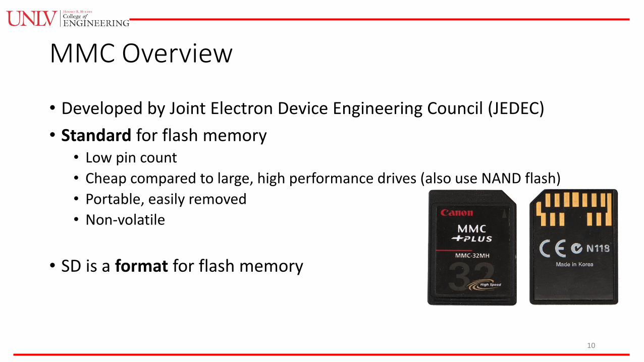
MMC Overview
• Developed by Joint Electron Device Engineering Council (JEDEC)
• Standard for flash memory• Low pin count
• Cheap compared to large, high performance drives (also use NAND flash)
• Portable, easily removed
• Non-volatile
• SD is a format for flash memory
10

Typical MMC Application System Overview
Source: JEDEC Standard No. 84-A441 Figure 3 11

MMC Adaptor Architecture
Source: JEDEC Standard No. 84-A441 Figure 16 12

MMC Architecture
Source: JEDEC Standard No. 84-A441 Figure 4 13
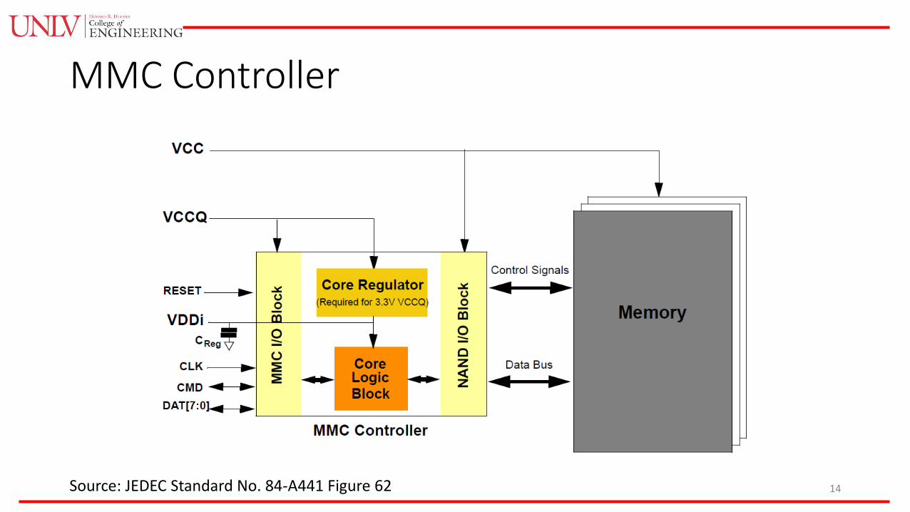
MMC Controller
Source: JEDEC Standard No. 84-A441 Figure 62 14

MMC Controller Power Supply Voltages
Source: JEDEC Standard No. 84-A441 Table 106 15

Flash Translation Layer (FTL)
• Functions• Logical to physical address mapping
• Power off recovery
• Wear leveling (erase/write counts)
• RAM tables and Flash map storage• Dangerous for recovery
• FTL algorithms determine physical address• Block/Sector/Hybrid Mapping
• Log Block Scheme
Source: Chung et al. Figure 1 16
Embedded MultiMedia Card (eMMC)
17

eMMC Overview
• Optimized for low power and small area
• Used in many mobile platforms: phones, microcontrollers, etc.
• Combines the flash controller, interface adapter, and memory arrays together on the same Silicon dye
• NOT removable (perfect for OS/firmware)
• Very affordable, low tier performance
• Reset signal is unique to eMMC vs other MMC applications
18

eMMC System Overview
Source: JEDEC Standard No. 84-B51 Figure 1 19
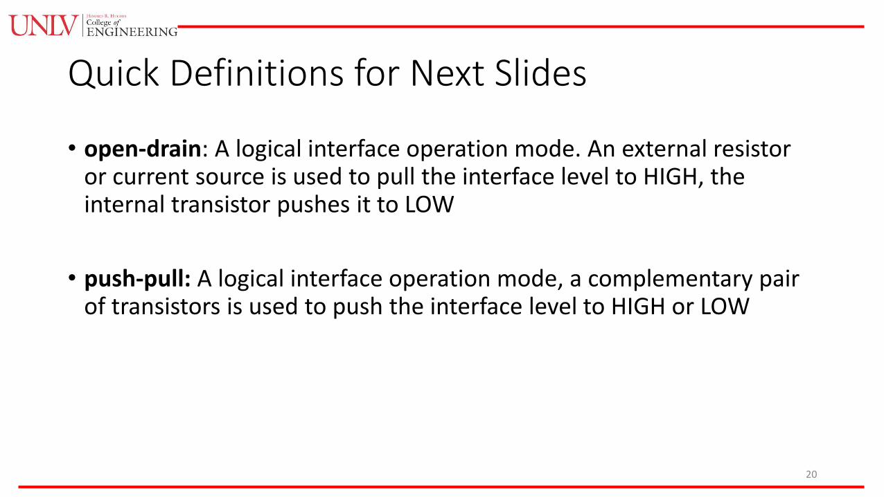
Quick Definitions for Next Slides
• open-drain: A logical interface operation mode. An external resistor or current source is used to pull the interface level to HIGH, the internal transistor pushes it to LOW
• push-pull: A logical interface operation mode, a complementary pair of transistors is used to push the interface level to HIGH or LOW
20

Communication
Source: JEDEC Standard No. 84-A441 Table 5 21

11 Signal Bus
• CLK: 0-200MHz
• Data Strobe: output in DDR mode• Data output on rise and falling edges• CMD and CRC status is still on rising edge
• CMD• Bidirectional command channel• Open drain for initialization and push-pull for fast command transfer
• DAT[0-7]• Defaults to DAT[0] after boot• Larger bus widths are negotiated after bootup
• Pull-ups disconnected when lines are in use
22

Load Capacitance
23Source: JEDEC Standard No. 84-B51 Table 200 / Page 247

Address Spaces
• Mapped Host Address Space• Usable space by the host software
• Private Vendor Specific Address Space• Cannot be accessed by read command by host• Contains firmware and mapping tables for the controller• No host data
• Unmapped Host Address Space• Cannot be read by host• May contain old host data or copies
• Reason why government does not like flash/SSD memory
• 32 bit addresses imply 2GB max unless multiple sectors are used (512B in size each)
24

Packet Formats & Operation
25

Multiple Read Operation
Source: JEDEC Standard No. 84-B51 Figure 2 26
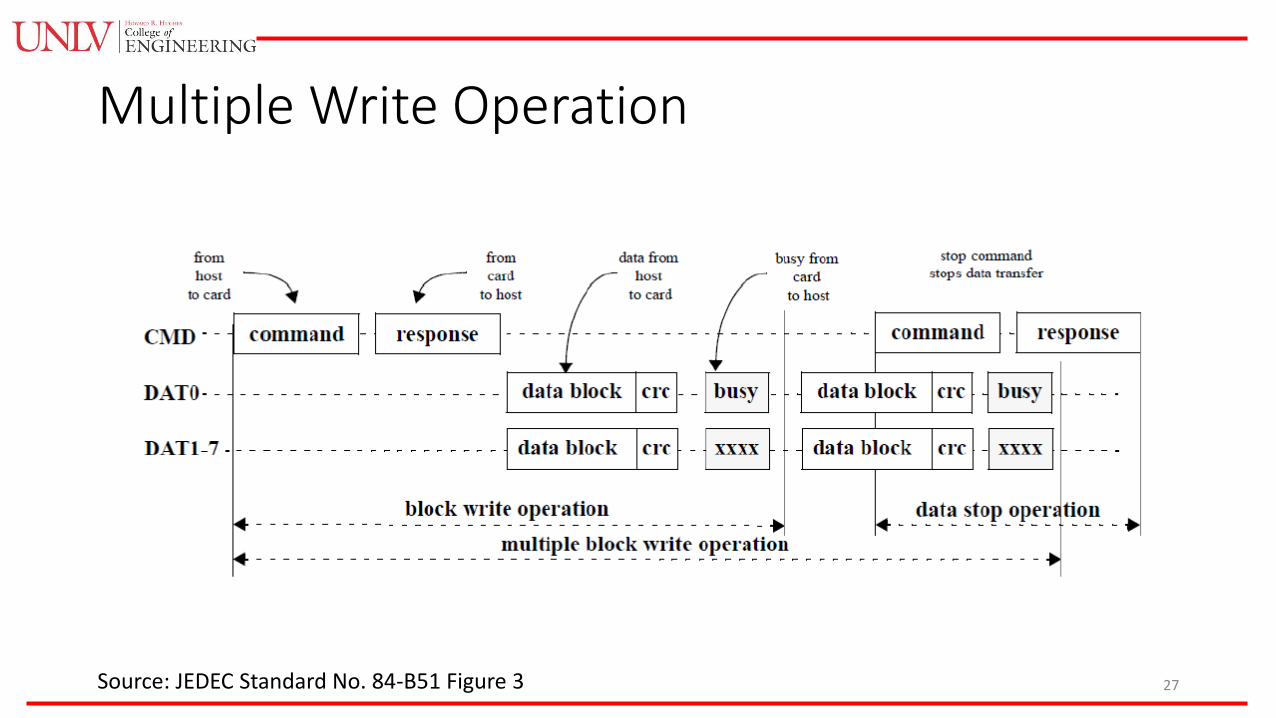
Multiple Write Operation
Source: JEDEC Standard No. 84-B51 Figure 3 27
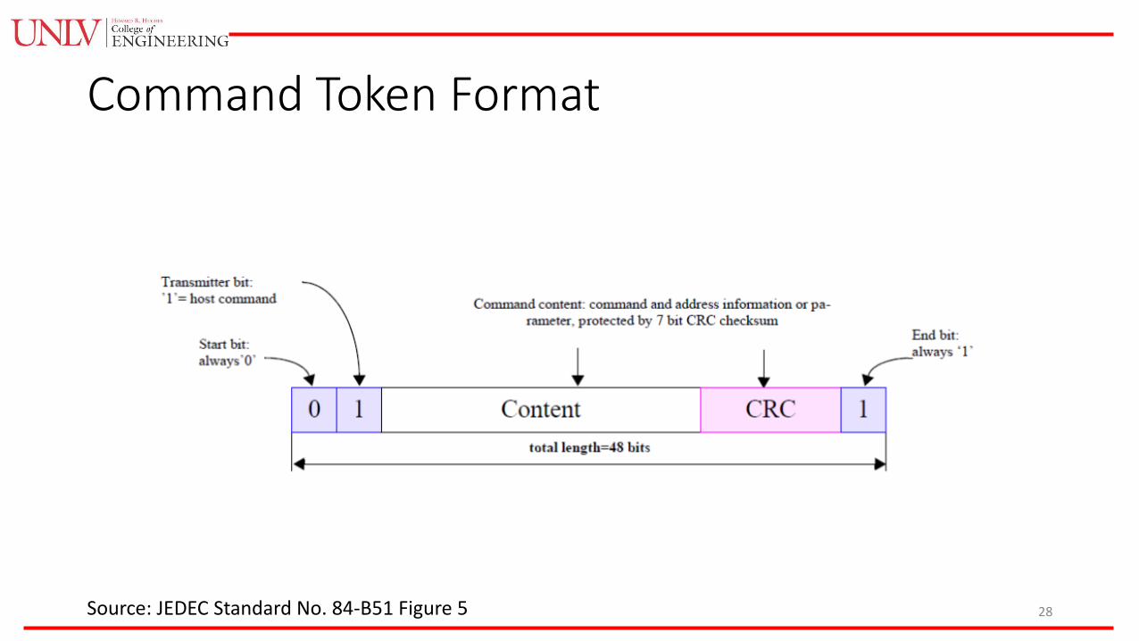
Command Token Format
Source: JEDEC Standard No. 84-B51 Figure 5 28

Quick Definitions for Next Slide
• CID: Card Identification number register
• CSD: Card Specific Data register
29

Response Token Format
Source: JEDEC Standard No. 84-B51 Figure 6 30

Single Bit Bus Data Packet Format for SDR
Source: JEDEC Standard No. 84-B51 Figure 7 31

4 Bit Bus Data Packet Format for SDR
Source: JEDEC Standard No. 84-B51 Figure 7 32

8 Bit Bus Data Packet Format for SDR
Source: JEDEC Standard No. 84-B51 Figure 7 33

Data Packet Format for DDR
Source: JEDEC Standard No. 84-B51 Figure 8 34

Bus Speed Modes
Source: JEDEC Standard No. 84-B51 Table 4 35
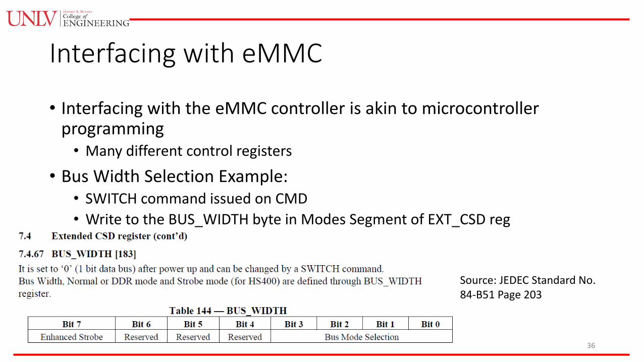
Interfacing with eMMC
Source: JEDEC Standard No. 84-B51 Page 203
• Interfacing with the eMMC controller is akin to microcontroller programming• Many different control registers
• Bus Width Selection Example:• SWITCH command issued on CMD
• Write to the BUS_WIDTH byte in Modes Segment of EXT_CSD reg
36

CRC 16 Generation (Payload)
Source: JEDEC Standard No. 84-A441 Figure 56 / Page 158 37

Higher Performing Technologies
38

Universal Flash Storage (UFS) Architecture Overview
39Source: JEDEC Standard No. 220C Figure 5-4 / 6-1

UFS Communication Overview
40Source: JEDEC Standard No. 220C Figure 5-1

Solid State Drive (SSD)
41Source: SSD Architecture and PCI Express Interface Figure 2.1 / 2.9

References
• CMOS Circuit Design, Layout, and Simulation, Third Edition – R. Jacob Bakerhttp://cmosedu.com/cmos1/book.htm
• A Survey of Flash Translation Layer – Tae-Sun Chung, et al.http://idke.ruc.edu.cn/people/dazhou/Papers/AsurveyFlash-JSA.pdf
• JEDEC Standard No. 84-A441https://www.jedec.org/standards-documents/docs/jesd84-a441
• JEDEC Standard No. 84-B51https://www.jedec.org/standards-documents/docs/jesd84-b51
• JEDEC Standard No. 220Chttps://www.jedec.org/standards-documents/docs/jesd220c
• SSD Architecture and PCI Express Interface – K. Eshghi & R. Michelonihttps://link.springer.com/chapter/10.1007%2F978-94-007-5146-0_2
42


