EMI Filter Design - ieca-inc. · PDF fileference that is conducted or radiated from the power...
28
P1: IML/OVY P2: IML/OVY QC: IML/OVY T1: IML MHBD017-03 Sandler MHBD017-Sandler-v4.cls October 6, 2005 18:53 Chapter 3 EMI Filter Design Nearly all power circuits contain an input electromagnetic interference (EMI) filter. The main purpose of the EMI filter is to limit the inter- ference that is conducted or radiated from the power circuit. Excessive conducted or radiated interference can cause erratic behavior in other systems that are in close proximity of, or that share an input source with, the power circuit. If this interference affects the power circuit, it can cause erratic operation, excessive ripple, or degraded regulation, which can lead to system level problems. Input EMI filters may also be used to limit inrush current, reduce conducted susceptibility, and suppress spikes. The specifications for the allowable interference are generally driven by the power circuit specification. The most common specifications include MIL-STD-461 for military applications and FCC for commercial applications. Many other EMI specifications also exist. This chapter will deal with the design and analysis of EMI filters that will reduce conducted interference and conducted susceptibility and limit inrush current. The design of the input filter is slightly more critical when the power circuit is a regulated switching circuit, rather than a linear circuit, because a negative input resistance is created by the regulated switching circuit. Although it is possible to simulate the radiated interference of a power circuit, it is beyond the scope of this book. Basic Requirements The design of an input EMI filter begins with the definition of two basic requirements: The filter must provide the power converter with lower output impe- dance than the negative input resistance of the power circuit. 63
Transcript of EMI Filter Design - ieca-inc. · PDF fileference that is conducted or radiated from the power...

P1: IML/OVY P2: IML/OVY QC: IML/OVY T1: IML
MHBD017-03 Sandler MHBD017-Sandler-v4.cls October 6, 2005 18:53
Chapter
3EMI Filter Design
Nearly all power circuits contain an input electromagnetic interference(EMI) filter. The main purpose of the EMI filter is to limit the inter-ference that is conducted or radiated from the power circuit. Excessiveconducted or radiated interference can cause erratic behavior in othersystems that are in close proximity of, or that share an input sourcewith, the power circuit. If this interference affects the power circuit, itcan cause erratic operation, excessive ripple, or degraded regulation,which can lead to system level problems. Input EMI filters may alsobe used to limit inrush current, reduce conducted susceptibility, andsuppress spikes. The specifications for the allowable interference aregenerally driven by the power circuit specification. The most commonspecifications include MIL-STD-461 for military applications and FCCfor commercial applications. Many other EMI specifications also exist.
This chapter will deal with the design and analysis of EMI filtersthat will reduce conducted interference and conducted susceptibilityand limit inrush current. The design of the input filter is slightly morecritical when the power circuit is a regulated switching circuit, ratherthan a linear circuit, because a negative input resistance is created bythe regulated switching circuit.
Although it is possible to simulate the radiated interference of apower circuit, it is beyond the scope of this book.
Basic Requirements
The design of an input EMI filter begins with the definition of two basicrequirements:
� The filter must provide the power converter with lower output impe-dance than the negative input resistance of the power circuit.
63

P1: IML/OVY P2: IML/OVY QC: IML/OVY T1: IML
MHBD017-03 Sandler MHBD017-Sandler-v4.cls October 6, 2005 18:53
64 Chapter Three
� The input filter attenuation must be sufficient to limit the resultinginterference to a level that is below the imposed specification.
The following flowchart provides a step-by-step approach that may beused to design an input filter.
EMI filter design flowchart
DefineImpedance
YES
YES
YES
NO
AttenuationDefined?
HarmonicContentKnown
NOWaveformKnown?
EstimateWaveform
Calculate Fouriercomponents
CalculateAttenuation
CalculatecomponentValues
Defining the Negative Resistance
The negative resistance of the power circuit can be defined by lookingat the following conditions
Pin = Pout
efficiency
Iin = Pin
Vin
Rin = Vin
Iin= V2
in
Pin= V2
in∗efficiency
Pout

P1: IML/OVY P2: IML/OVY QC: IML/OVY T1: IML
MHBD017-03 Sandler MHBD017-Sandler-v4.cls October 6, 2005 18:53
EMI Filter Design 65
The input resistance is negative because as the input voltage in-creases, the input current decreases. As a simple example, we can usePSpice to analyze the input resistance of the power circuit. PSpice cananalyze the input resistance in a number of ways. The simplest methodis the transfer function (.TF) analysis, which calculates the DC gainand the small signal input and output impedance. The following exam-ple uses the PSpice.TF analysis to measure the input resistance of aswitching power circuit.
Example 1—Input resistance analysis
Input FileRIN: INPUT RESISTANCE.TF V(5) V1V1 5 0 20G1 5 0 Value = { 100/V(5) }.END
Output FileRIN: INPUT RESISTANCE.TF V(5) V1V1 5 0 20G1 5 0 Value = { 100/V(5) }.END
.END∗∗∗SMALL-SIGNAL CHARACTERISTICS
V(5)/V1 = 1.000E+00
INPUT RESISTANCE AT V1 = −4.004E+00
OUTPUT RESISTANCE AT V(5) = 0.000E+00
The G1 source simulates a power circuit, which has an input power of100 W. V1 applies 20 VDC to the power circuit, and the .TF measuresthe input impedance at node 5 and the output impedance at V1. Theresults are placed in the output file. Note that PSpice calculated theinput impedance as a negative resistance of 4 �, which is in agreementwith the above derivation.
Defining the Harmonic Content
The next step in designing an input EMI filter is to determine the har-monic content of the power circuit input current. If the input currentwaveform is known, a Fourier analysis can be performed in order to es-tablish the harmonic content of the waveform; however, even if the exactwaveform is not known, we can estimate the waveform with reasonableaccuracy. The design can be optimized later, if necessary.
Consider the pulsating waveform in Fig. 3.1. With a peak amplitudeof 1 and a base amplitude of 0, we can compute the Fourier series of

P1: IML/OVY P2: IML/OVY QC: IML/OVY T1: IML
MHBD017-03 Sandler MHBD017-Sandler-v4.cls October 6, 2005 18:53
66 Chapter Three
Input Current 1 0
t
T
Duty Cycle = t/T
Figure 3.1 Pulsating waveform used in the Fourier series computation.
harmonic n as follows:
An = 2T
t∫0
sin(nt)
Bn = 2T
t∫0
cos(nt)
Cn =√
A2n + B2
n
If we assume that the input ripple current is pulsating and if weknow the duty cycle, we can proceed to the Fourier analysis. If theduty cycle is not known, we will assume a value of 50%. This assump-tion is the worst case, because the Fourier analysis of a pulsed wave-form has a maxima at a value of 50%. In the next example, we willuse SPICE to calculate the Fourier coefficients of a 50% duty cyclepulse.
Example 2—.FOUR analysis
The following example demonstrates the use of the .FOUR analysis. V1is a pulsed voltage source, which has a 50% duty cycle and a 100-kHzfrequency. The .FOUR statement calculates the magnitude and phaseof the DC value and the first nine harmonics. The result is placed inthe output file as shown below.
EX2: DEMONSTRATING THE USE OF THE .FOUR ANALYSIS.OPTIONS NUMDGT=3.TRAN .01U 20U.FOUR 100KHZ V(1)V1 1 0 PULSE 0 1 0 0 0 5U 10U.END

P1: IML/OVY P2: IML/OVY QC: IML/OVY T1: IML
MHBD017-03 Sandler MHBD017-Sandler-v4.cls October 6, 2005 18:53
EMI Filter Design 67
FOURIER COMPONENTS OF TRANSIENT RESPONSE V(1)
DC COMPONENT = 5.010000E-01
HARMONIC FREQUENCY FOURIER NORMALIZED PHASE NORMALIZEDNO (Hz) COMPONENT COMPONENT (DEG) PHASE(DEG)1 1.000E+05 6.366E-01 1.000E+00 -3.600E-01 0.000E+002 2.000E+05 2.000E-03 3.142E-03 8.928E+01 9.000E+013 3.000E+05 2.122E-01 3.333E-01 -1.080E+00 4.088E-094 4.000E+05 2.000E-03 3.142E-03 8.856E+01 9.000E+015 5.000E+05 1.273E-01 2.000E-01 -1.800E+00 2.044E-086 6.000E+05 2.000E-03 3.142E-03 8.784E+01 9.000E+017 7.000E+05 9.093E-02 1.428E-01 -2.520E+00 5.723E-088 8.000E+05 2.000E-03 3.142E-03 8.712E+01 9.000E+019 9.000E+05 7.072E-02 1.111E-01 -3.240E+00 1.226E-07
TOTAL HARMONIC DISTORTION = 4.288115E+01 PERCENT
As you can see from the output file, the fundamental harmonic hasa peak value that is 63.6% of the peak pulse amplitude. Although thisdoes provide the required information, it is far from elegant. A bettersolution is to calculate the harmonics in Probe. The resulting plot isshown in Fig. 3.2.
This is the worst case for a pulsed waveform and could be conserva-tively used for the design of the input filter.
Example 3—Using the .STEP command to calculate harmonics
The next example uses the PSpice .STEP command to sweep the dutycycle from 5% to 95% and look at the fundamental amplitude of theresulting square wave. As in the previous example, V1 is a pulsed
Frequency
0Hz 0.5MHz 1.0MHz 1.5MHz 2.0MHz 2.5MHz 3.0MHz 3.5MHz 4.0MHz 4.5MHz 5.0MHzV(1)
0V
400mV
800mV
SEL>>
Time
0s 2us 4us 6us 8us 10us 12us 14us 16us 18us 20usV(1)
0V
0.5V
1.0V
Figure 3.2 The FFT feature of the Probe graphical waveform postprocessor is used tocalculate the harmonics of a square waveform.

P1: IML/OVY P2: IML/OVY QC: IML/OVY T1: IML
MHBD017-03 Sandler MHBD017-Sandler-v4.cls October 6, 2005 18:53
68 Chapter Three
Frequency
0Hz 40KHz 80KHz 120KHz 160KHz 200KHz 240KHz 280KHz 320KHz 360KHz 400KHz 440KHz... V(1)-V(0)
0V
0.2V
0.4V
0.6V
0.8V
1.0V
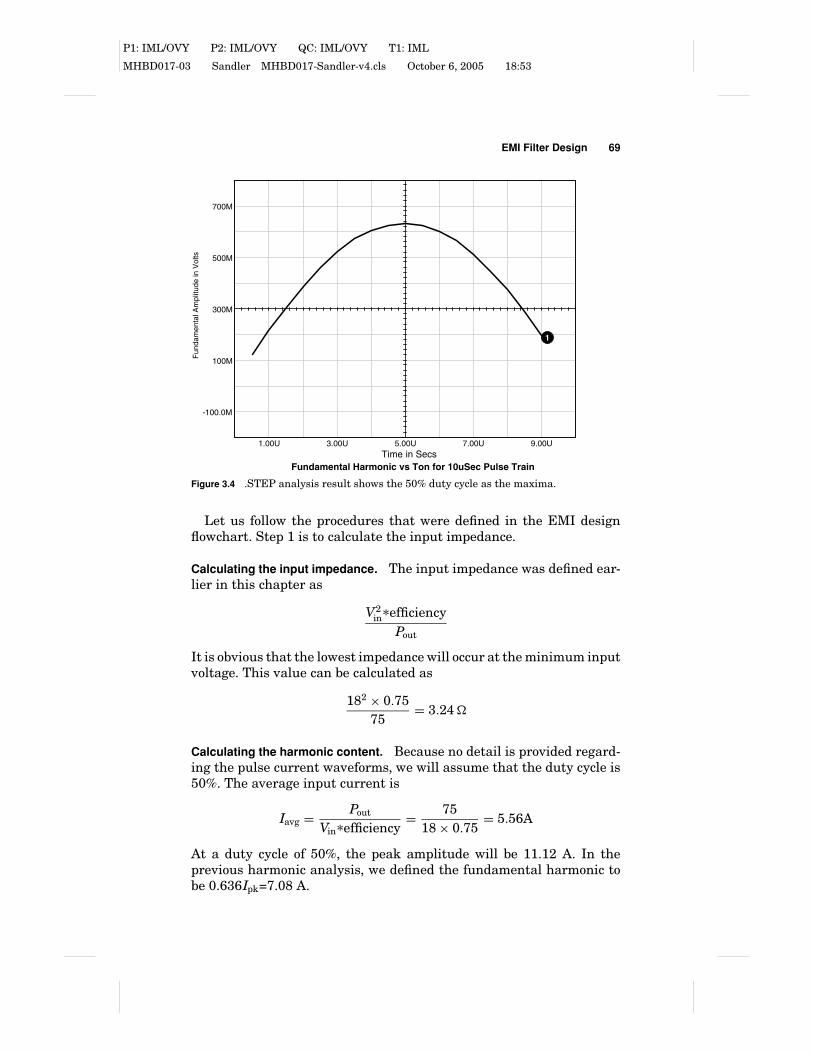
Figure 3.3 FFT of the .STEP analysis. The waveform with the largest amplitude at 100kHz corresponds to the 50% duty cycle (TON= 5 µs).
voltage source. In this case, the pulse has an initial amplitude of1 V and switches to 0 V after delay “TON.” “TON” is swept from 0.5 to9.5 µs in 0.5-µs steps.
When the simulation is finished, you can use Probe to display theX-Y data, or you may view the output file in a text editor. You willhave a graph of the fundamental harmonic versus “TON.” This confirmsthe previous statement that the 50% duty cycle was the maxima andprovides a reference you may find helpful in the future.
X3: .STEP ANALYSIS.PROBE.PARAM TON=0.5u.STEP PARAM TON 0.5u 9.5u 0.5u.TRAN .1U 10U.PRINT TRAN V(1)V1 1 0 PULSE 1 0 {TON}.END
The FFT results of the .STEP analysis are shown in the graphs ofFigs. 3.3 and 3.4.
Example 4 – EMI filter design
In order to design the EMI filter, we need to define a converter thatwill operate with it. For the purpose of this example, let us assume thatwe have a power converter that will operate with an input voltage of18 to 32 V DC. The converter output power will be 75 W and will havean operating efficiency of 75%. The converter will have a switchingfrequency of 100 kHz. The conducted emissions requirement allows the1-mA peak to be reflected back to the input lines. A second-order filterwill be used.
P1: IML/OVY P2: IML/OVY QC: IML/OVY T1: IML
MHBD017-03 Sandler MHBD017-Sandler-v4.cls October 6, 2005 18:53
EMI Filter Design 69
1
1.00U 3.00U 5.00U 7.00U 9.00UTime in Secs
700M
500M
300M
100M
-100.0M
Fun
dam
enta
l Am
plitu
de in
Vol
ts
Fundamental Harmonic vs Ton for 10uSec Pulse Train
Figure 3.4 .STEP analysis result shows the 50% duty cycle as the maxima.
Let us follow the procedures that were defined in the EMI designflowchart. Step 1 is to calculate the input impedance.
Calculating the input impedance. The input impedance was defined ear-lier in this chapter as
V2in
∗efficiencyPout
It is obvious that the lowest impedance will occur at the minimum inputvoltage. This value can be calculated as
182 × 0.7575
= 3.24 �
Calculating the harmonic content. Because no detail is provided regard-ing the pulse current waveforms, we will assume that the duty cycle is50%. The average input current is
Iavg = Pout
Vin∗efficiency= 75
18 × 0.75= 5.56A
At a duty cycle of 50%, the peak amplitude will be 11.12 A. In theprevious harmonic analysis, we defined the fundamental harmonic tobe 0.636Ipk=7.08 A.

P1: IML/OVY P2: IML/OVY QC: IML/OVY T1: IML
MHBD017-03 Sandler MHBD017-Sandler-v4.cls October 6, 2005 18:53
70 Chapter Three
Calculating the required attenuation. With a maximum reflected ripplecurrent of 1-mA peak, we can define the attenuation required as
Attenuation = 7.080.001
= 7080 = 77 dB
Calculating the component values. The attenuation for a second-orderfilter can be defined as
Attenuation =(
fswitch
ffilter
)2
We can compute the filter frequency as
100 kHz√Attenuation
= 100 kHz84.14
= 1188 Hz.
The values of L and C can be defined by setting their impedances tothe input converter input impedance at the filter resonant frequency,as defined above.
C = 12π
(1188
) (3.24
) = 41.35 µF
L = 3.242π
(1188
)434 µH
Note that the characteristic impedance of the filter is defined by
Zo =√
LC
=√
434 µH41.35 µF
= 3.24 �
which is equal to the converter input impedance. In an actual design,it is a good practice to provide a 6-dB margin for these characteristics.
Damping Elements
While this filter provides the proper impedance matching and the re-quired attenuation, the impedance will be quite high at the resonantfrequency of the filter. The only damping elements in the circuit are theDC resistance (DCR) of the inductor and the equivalent series resis-tance (ESR) of the capacitor (which we have not defined). It is normallynecessary to provide damping of the L-C filter in order to restrict theimpedance of the filter at the resonant frequency. A shunt series R-Cnetwork is used for this purpose. The value of the damping capacitoris generally 3 to 5 times greater than that of the filter capacitor, and

P1: IML/OVY P2: IML/OVY QC: IML/OVY T1: IML
MHBD017-03 Sandler MHBD017-Sandler-v4.cls October 6, 2005 18:53
EMI Filter Design 71
C141.35U
C2CDAMP I1
AC
V(1)
R1RDAMP
1
2
Frequency
100Hz 300Hz 1.0KHz 3.0KHz 10KHz 30KHz 100KHz 300KHz 1.0MHzV(1)
0V
1.0V
2.0V
3.0V
4.0V
Figure 3.5 Schematic of the test circuit used to measure the impedance of the filter. Thewaveform V(1) is equivalent to the impedance because the input is a current (I1 1 0 AC1). The case for CDAMP = 120µ and RDAMP = 1.6 is shown.
the value of the damping resistor is generally close to the characteristicimpedance of the filter. The PSpice .Step command is ideal for definingthese elements.
The following circuit is designed to measure the impedance of the fil-ter, while sweeping the damping capacitor from 120 to 200 µF in 40-µFincrements. For each value of the damping capacitor, the damping re-sistor will be swept from 0.5 to 2 times the characteristic impedance(1.6 to 6.4 �) in 0.6-� increments. The PSpice listing and schematic ofthe test circuit (Fig. 3.5) are shown below.
The results are shown below.
EX4: TO MEASURE THE IMPEDANCE OF A FILTER.AC DEC 10 100HZ 1MEGHZ.PARAM CDAMP=120u.PARAM RDAMP=1.6.STEP PARAM CDAMP 120U 200U 40U.STEP PARAM RDAMP 1.6 6.4 .6.PROBEC1 1 0 41.35U

P1: IML/OVY P2: IML/OVY QC: IML/OVY T1: IML
MHBD017-03 Sandler MHBD017-Sandler-v4.cls October 6, 2005 18:53
72 Chapter Three
C2 1 2 {CDAMP}R1 2 0 {RDAMP}I1 0 1 AC 1L1 0 1 434U.END
The results are provided in the output file and are shown below.
Sweep Analysis of EX4.ckt
Count CDAMPRDAMPMaximum1 1.20000e-004 1.60000e+000 3.8912 1.20000e-004 2.20000e+000 3.4403 1.20000e-004 2.80000e+000 3.5574 1.20000e-004 3.40000e+000 3.9165 1.20000e-004 4.00000e+000 4.3956 1.20000e-004 4.60000e+000 4.8407 1.20000e-004 5.20000e+000 5.2488 1.20000e-004 5.80000e+000 5.6199 1.20000e-004 6.40000e+000 6.104
10 1.60000e-004 1.60000e+000 2.99411 1.60000e-004 2.20000e+000 2.86912 1.60000e-004 2.80000e+000 3.15313 1.60000e-004 3.40000e+000 3.67214 1.60000e-004 4.00000e+000 4.16115 1.60000e-004 4.60000e+000 4.61416 1.60000e-004 5.20000e+000 5.03317 1.60000e-004 5.80000e+000 5.58018 1.60000e-004 6.40000e+000 6.12119 2.00000e-004 1.60000e+000 2.48920 2.00000e-004 2.20000e+000 2.59321 2.00000e-004 2.80000e+000 3.02422 2.00000e-004 3.40000e+000 3.54723 2.00000e-004 4.00000e+000 4.03824 2.00000e-004 4.60000e+000 4.49425 2.00000e-004 5.20000e+000 5.04026 2.00000e-004 5.80000e+000 5.59127 2.00000e-004 6.40000e+000 6.137
The impedance was exceeded with the 120-µF damping capacitor(Fig. 3.6). If we use a 160-µF capacitor, the impedance will be minimizedwith a 2.2-� damping resistor. A lower impedance could be achievedwith a 200-µF damping capacitor and a 1.6-� damping resistor. Wewill select the 160-µF capacitor and the 2.2-� resistor.
The following simulation shows the impedance characteristics andthe reflected ripple of the filter (see also Figs. 3.7 and 3.8).
EMI2: TO SHOW THE REFLECTED RIPPLE OF THE FILTER.AC DEC 10 100HZ 100KHZ.TRAN 1U 10M 9980U .1u UIC.PROBE

P1: IML/OVY P2: IML/OVY QC: IML/OVY T1: IML
MHBD017-03 Sandler MHBD017-Sandler-v4.cls October 6, 2005 18:53
EMI Filter Design 73
1
2.10 3.10 4.10 5.10 6.10Rdamp
6.00
5.00
4.00
3.00
2.00
Max
imum
inpe
danc
e in
Ohm
s
C=120 µF
C=200 µF
C=160 µF
Figure 3.6 Family of curves showing the maximum impedance versus the damping resis-tor value. Each curve represents a different capacitor value.
C1 2 0 41.35UC2 2 1 160UR1 1 0 2.2I1 0 2 AC 1 PULSE 0 11 0.1U 0.1U 0.1U 5U 10UL1 0 2 434U IC=-5.5.END
L1434U
C141.35U
C2160U
R12.2
I1AC
V(2)
I(V1)L1[I]4
2
1
Figure 3.7 Circuit used to show the impedance and the reflected ripple of the filter.

P1: IML/OVY P2: IML/OVY QC: IML/OVY T1: IML
MHBD017-03 Sandler MHBD017-Sandler-v4.cls October 6, 2005 18:53
74 Chapter Three
9.988M-5.611<
x>
9.993M-5.609<
x>
1
9.982M 9.986M 9.990M 9.994M 9.998MTime in Secs
-5.608
-5.609
-5.610
-5.611
-5.612
Indu
ctor
Cur
rent
in A
mps
∆x = 5.050U ∆y = 1.908M
1
200 500 1K 2K 5K 10K 20K 50KFrequency in Hz
3.50
2.50
1.50
500M
-500M
Filt
er Im
peda
nce
V(2
) in
Am
ps
(a)
(b)
Figure 3.8 Current in the inductor (a) due to a current pulse input, andimpedance characteristics over frequency (b) for the filter circuit in Fig. 3.7.
Fourth-Order Filters
Because the physical size of power converters is continually shrinking,higher order filters are being used more often than not. The filter is

P1: IML/OVY P2: IML/OVY QC: IML/OVY T1: IML
MHBD017-03 Sandler MHBD017-Sandler-v4.cls October 6, 2005 18:53
EMI Filter Design 75
designed in much the same way as the second-order filter. The followingexample demonstrates the design of a fourth-order filter using the samedesign parameters as those that we used for the previous filter.
The “octave” rule basically states that resonances should be at leastan octave apart. In an effort to be conservative, let us use a factor of2.5. The attenuation of the filter can be defined as
Attenuation =(
fswitch
f1
)2
∗(
fswitch
2.5 f1
)2
= f 4switch
6.25 f 41
If we set the attenuation at 7080, as in the previous example, andsolve for f1 we obtain f1=6.895 kHz. The second pole is then at 2.5 f1 =17.237 kHz.
The impedance of each section should be designed to be lower than theimpedance of the converter, which we had determined to be 3.24 � inthe previous example. The filter is loaded by the negative resistance ofthe converter and produces a combined impedance of
Zloaded = Zin ∗ Zo
Zin + Zo
The loaded filter Q is defined as
Q = Zloaded
Zo
where Zo is the filter characteristic impedance defined by
Zo =√
LC
If we combine the above equations, we have
Q = Zin ∗ Zo
(Zin + Zo) Zo
Zo = −(
Q − 1Q
)Zin
The filter Q is generally maintained below a value of 2. If we set Q = 2and solve for Zo we obtain
Zo = −(
2 − 12
) (−3.24) = 1.62 �

P1: IML/OVY P2: IML/OVY QC: IML/OVY T1: IML
MHBD017-03 Sandler MHBD017-Sandler-v4.cls October 6, 2005 18:53
76 Chapter Three
If we use this impedance and the calculated resonant frequencies, wecan define both inductors and both capacitors.
L1 = 1.622π
(6895
) = 37 µH
C1 = 12π
(6895
) (1.62
) = 14 µF
L2 = 1.622π
(17, 237
) = 15 µH
C2 = 12π
(17, 237
) (1.62
) = 5.7 µF
As shown in the previous example, we can use the .Step command tosweep the values of the damping capacitor and the damping resistor. Ifwe use a range of 3 to 5 times the value of the real capacitor, we willsweep the damper capacitor from 42 to 70 µF in steps of 14 µF. We willsweep the damper resistor from one-half to twice the Zo of the filter,i.e., from 0.8 to 3.2 � in 0.2-� steps.
The schematic for the fourth-order filter and its impedance responseare shown in Fig. 3.9.
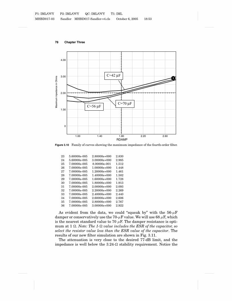
Note that two 10-M� resistors have been added. To aid circuit con-vergence, the resistors were added to the nodes that are purely reactive.The circuit listing and output file are shown below. A sweep of the maxi-mum impedance as a function of the damping resistor and the dampingcapacitor was also performed. The results of the sweep are shown inFig. 3.10. Each curve is for a different value of damping capacitor.
4THORD: A 4TH ORDER FILTER.AC DEC 10 100HZ 1MEGHZ.PROBE.PARAM CDAMP=42u.PARAM RDAMP=0.8.STEP PARAM CDAMP 42U 70U 14U∗.STEP PARAMRDAMP .8 3.2 .2.PRINT AC V(4) VP(4)1 1 0 5.7UC2 4 2 {CDAMP}R1 2 0 {RDAMP}I1 0 4 AC 1L2 1 4 37UC3 4 0 14UR2 1 0 10MEGR3 4 0 10MEGL1 0 1 15U.END

P1: IML/OVY P2: IML/OVY QC: IML/OVY T1: IML
MHBD017-03 Sandler MHBD017-Sandler-v4.cls October 6, 2005 18:53
EMI Filter Design 77
L1 15U
C15.7U
C2CDAMP
R1RDAMP
I1AC
V(4)L2 37U
C314U
R210MEG R3
10MEG
1 4
2
100Hz 300Hz 1.0KHz 3.0KHz
Frequency
10KHz 30KHz 100KHz 300KHz 1.0MHzV(4)
0V
0.5V
1.0V
1.5V
2.0V
2.5V
3.0V
Figure 3.9 Fourth-order filter schematic and impedance response.
Count CDAMPRDAMPMaximum
1 4.20000e-005 8.00000e-001 2.5072 4.20000e-005 1.00000e+000 2.2153 4.20000e-005 1.20000e+000 2.0274 4.20000e-005 1.40000e+000 2.0245 4.20000e-005 1.60000e+000 2.0836 4.20000e-005 1.80000e+000 2.1337 4.20000e-005 2.00000e+000 2.2858 4.20000e-005 2.20000e+000 2.4589 4.20000e-005 2.40000e+000 2.62710 4.20000e-005 2.60000e+000 2.79111 4.20000e-005 2.80000e+000 2.95012 4.20000e-005 3.00000e+000 3.10313 5.60000e-005 8.00000e-001 1.79914 5.60000e-005 1.00000e+000 1.71615 5.60000e-005 1.20000e+000 1.65916 5.60000e-005 1.40000e+000 1.72717 5.60000e-005 1.60000e+000 1.82018 5.60000e-005 1.80000e+000 1.97919 5.60000e-005 2.00000e+000 2.15820 5.60000e-005 2.20000e+000 2.33421 5.60000e-005 2.40000e+000 2.50522 5.60000e-005 2.60000e+000 2.670
P1: IML/OVY P2: IML/OVY QC: IML/OVY T1: IML
MHBD017-03 Sandler MHBD017-Sandler-v4.cls October 6, 2005 18:53
78 Chapter Three
1
1.00 1.40 1.80 2.20 2.60RDAMP
4.00
3.00
2.00
1.00
0
Max
imum
inpe
danc
e in
Ohm
s C=42 µF
C=70 µF C=56 µF
Figure 3.10 Family of curves showing the maximum impedance of the fourth-order filter.
23 5.60000e-005 2.80000e+000 2.83024 5.60000e-005 3.00000e+000 2.98525 7.00000e-005 8.00000e-001 1.51226 7.00000e-005 1.00000e+000 1.44827 7.00000e-005 1.20000e+000 1.46128 7.00000e-005 1.40000e+000 1.58229 7.00000e-005 1.60000e+000 1.72830 7.00000e-005 1.80000e+000 1.91331 7.00000e-005 2.00000e+000 2.09332 7.00000e-005 2.20000e+000 2.26933 7.00000e-005 2.40000e+000 2.44034 7.00000e-005 2.60000e+000 2.60635 7.00000e-005 2.80000e+000 2.76736 7.00000e-005 3.00000e+000 2.922
As evident from the data, we could “squeak by” with the 56-µFdamper or conservatively use the 70-µF value. We will use 68 µF, whichis the nearest standard value to 70 µF. The damper resistance is opti-mum at 1 �. Note: The 1-� value includes the ESR of the capacitor, soselect the resistor value less than the ESR value of the capacitor. Theresults of our new filter simulation are shown in Fig. 3.11.
The attenuation is very close to the desired 77-dB limit, and theimpedance is well below the 3.24-� stability requirement. Notice the

P1: IML/OVY P2: IML/OVY QC: IML/OVY T1: IML
MHBD017-03 Sandler MHBD017-Sandler-v4.cls October 6, 2005 18:53
EMI Filter Design 79
100.0K-76.4<
x
>
11K 10K 100K
Frequency in Hz
20.0
-20.0
-60.0
-100.0
-140
Atte
nuat
ion
in d
B (
Am
ps)
Figure 3.11 The filter attenuation using the optimized values for the damper section.
peaking of the undamped first stage of the filter. The .STEP analysismay be used to determine optimum values for the damper section also,if desired. We will use the same capacitor ratio as we had determined forthe second stage. This yields a damper capacitor value of approximately33 µF, and we will use the same 1-� value for the damper resistor. Whilewe are at it, let us change the 5.7-µF capacitor to 6.8 µF in order to ob-tain a standard value and to slightly improve the attenuation. Noticethat the peaking of the first stage has nearly been eliminated, andthe attenuation has been improved to meet the requirement of 77 dB(Fig. 3.12).
Inrush Current
In many applications, the input voltage is applied as a step. This maybe the result of a switch or relay closure. The current that is drawn bythe filter during this application of power is referred to as the inrushcurrent. The inrush current may be of concern, because of stress orfuse ratings. We can evaluate the inrush characteristics of our filter byapplying a step input from 0 V to the maximum input voltage (32 V inour design) while monitoring the current that is drawn by our filter.
Note that we can use the same model for both the AC and transientanalyses. The results of the inrush current simulation are shown in Fig.3.13. The inrush current has a peak value of 34 A. The output voltage

P1: IML/OVY P2: IML/OVY QC: IML/OVY T1: IML
MHBD017-03 Sandler MHBD017-Sandler-v4.cls October 6, 2005 18:53
80 Chapter Three
3.16K1.44<
x
>
1
1K 10K 100K
Frequency in Hz
1.40
1.00
600M
200M
-200M
Impe
danc
e in
Ohm
s
100.0K-79.4<
x
>
11K 10K 100K
Frequency in Hz
20.0
-20.0
-60.0
-100.0
-140
Filt
er a
ttenu
atio
n in
dB
(A
mps
)
Figure 3.12 The filter attenuation graph shows the elimination of the peaking in the firststage after changes in the damper section.

P1: IML/OVY P2: IML/OVY QC: IML/OVY T1: IML
MHBD017-03 Sandler MHBD017-Sandler-v4.cls October 6, 2005 18:53
EMI Filter Design 81
1
2
34C268U
C314U
R11
R210MEG R3
10MEG
L115U
L237U
I1AC = 1
V1 C16.8U
V_1IL1
5
C433U
R41
0s 50us 100us 150us 200us 250us
Frequency
300us 350us 400us 450us 500usI(L1) V(1)
-10
0
10
20
30
40
50
Figure 3.13 Schematic, netlist, and simulation results for the inrush current simulation.
of the filter is also displayed. When a 32-V step voltage was applied, thefilter output overshot to almost 48 V. This is an important considerationfor selecting and derating the components that are used in the switchingconverter that follows the filter.
4THORD2.cir.AC DEC 10 100 1meg.TRAN 1u 500u.PROBEC2 1 2 68UC3 1 0 14UR1 2 0 1R2 3 0 10MEGR3 1 0 10MEGL1 4 3 15UL2 3 1 37UI1 0 1 AC=1

P1: IML/OVY P2: IML/OVY QC: IML/OVY T1: IML
MHBD017-03 Sandler MHBD017-Sandler-v4.cls October 6, 2005 18:53
82 Chapter Three
V1 4 0 PULSE 0 32C1 3 0 6.8UC4 3 5 33UR4 5 0 1.END
MPP Inductors
The previous example utilized ideal inductors. In real applications,however, the inductors generally do not provide a constant inductance.Rather, they tend to saturate as current is passed through them. One ofthe more popular cores used in these applications is Magnetics
R©MPP
style.Using MPP cores for our EMI filter provides a more realistic model
than the ideal inductor model. The following simulations use a Magnet-ics 55131 core with 29 turns for the 15-µH inductor and a Magnetics55121 core with 36 turns for the 37-µH inductor (Fig. 3.14). DC resis-tances are 0.035 � and 0.025 �, respectively. Note the third terminalon the inductor symbol. The extra terminal is used to monitor the in-stantaneous inductance value.
4THINRS3.cir.PROBE.AC DEC 10 100 1meg.TRAN .1u 500u 0 .5uC2 2 3 68UC3 2 0 14UR1 3 0 1C4 1 7 33UR2 1 0 10MEGR3 2 0 10MEGR4 7 0 1I1 0 2 AC=1 ; DC=-4.5 used for Figure 3.16X1 6 1 8 MP55131 Params: N=29 DCR=.035 IC=0X2 1 2 9 MP55121 Params: N=36 DCR=.035 IC=0V1 4 0 PULSE 0 32V2 4 6C1 1 0 6.8U.END
This simulation also calculates the attenuation and impedance of thefilter without DC current using the AC analysis (Fig. 3.15).
If we add a DC current value of 4.5 A (100 W/22 V), we will see the datafor the filter as it operates under full load conditions. The inductanceof each MPP core can be monitored using markers as the simulationprogresses. The schematic will provide the values at the steady statecondition. If we view the inductance, we will see the value of inductanceduring the inrush current.

P1: IML/OVY P2: IML/OVY QC: IML/OVY T1: IML
MHBD017-03 Sandler MHBD017-Sandler-v4.cls October 6, 2005 18:53
EMI Filter Design 83
2
3
1
7
9
4
6
8
C268U
C314U
R11
C433U
R210MEG
R310MEG
R41
I1AC = 1
X2MP55121
V1
V2
C16.8U
Vout
Iin
Inductance2
X1MP55131 Inductance1
Time
0s 50us 100us 150us 200us 250us 300us 350us 400us 450us 500usV(2) I(V2)
0
25
50
75
100
SEL>>
V(8) V(9)0V
25uV
50uV
Figure 3.14 A more realistic simulation using MPP cores for EMI filter design. The in-stantaneous inductance is shown for both MPP cores (top graph) and for the input currentand output voltage.
The first simulation in Fig. 3.14 showed the results of the simulationwithout DC current. As you can see, the inrush current is considerablyhigher than the value we expected in the first simulation. This is dueto the saturation of the inductors. The waveforms in Fig. 3.14 show theinductance during the inrush current.
The input inductor is almost completely saturated by the inrush cur-rent. The inductance value in the schematic is somewhat higher thanthe design value.
The second simulation in Figs. 3.16 and 3.17 shows the results of thesimulation with a DC value of 4.5 A added to the current source I1.
The current is negative because of the direction of the current source.The inductor values are almost identical to the design values. The in-rush current analysis has not been performed, because it is unrealistic

P1: IML/OVY P2: IML/OVY QC: IML/OVY T1: IML
MHBD017-03 Sandler MHBD017-Sandler-v4.cls October 6, 2005 18:53
84 Chapter Three
100.0K-83.9<
x
>
11K 10K 100K
Frequency in Hz
20.0
-20.0
-60.0
-100.0
-140
Atte
nuat
ion
in d
B (
Am
ps)
Figure 3.15 Simulation result of the attenuation without a DC current.
to have the 4.5-A current flowing when the converter is turned on.The attenuation analysis was performed, and the results are shown inFig. 3.17.
The attenuation has been degraded by approximately 4 dB as a re-sult of the DC current; however, it is still sufficient to meet the 77-dBrequirement.
2
3
1
7
9
4
6
8
C268U
C314U
R11
C433U
R210MEG
R310MEG
R41
I1AC = 1-4.5
X2MP55121
V1
V2
C16.8U
Vout
Iin
Inductance2
X1MP55131 Inductance1
Figure 3.16 A realistic model using MPP cores with a 4.5-A steady state current.

P1: IML/OVY P2: IML/OVY QC: IML/OVY T1: IML
MHBD017-03 Sandler MHBD017-Sandler-v4.cls October 6, 2005 18:53
EMI Filter Design 85
100.0K-83.9<
x
>
11K 10K 100K
Frequency in Hz
20.0
-20.0
-60.0
-100.0
-140
Atte
nuat
ion
in d
B (
Am
ps)
Figure 3.17 Effect of the DC current on the attenuation analysis.
The inrush current simulation is one of the most difficult simulationsto correlate with real hardware. This is generally due to the effects ofthe source impedance of the test setup. Keep in mind that the powersupplies and cables have resistance and inductance. The SPICE modelmust account for these elements, or they must absolutely be minimized.With this in mind, it is certainly feasible to get good correlation with alittle care.
The example circuit in Fig. 3.18 was constructed for the purpose ofdetermining the accuracy of the model. The 28.8-µH input inductor isconstructed as 24 turns on a 58271 core, and the two 25.1-µH inductorsare constructed as 28 turns on two stacked 58291 cores. The results areshown in Figs. 3.19 and 3.20. The inductance of these two inductors isshown in Fig. 3.18. Note that the input inductor drops by more than60% as a result of the inrush current.
emi inrush correlation.cir.PROBE.TRAN 10n 250u 0 50nC2 10 11 3UC3 9 2 1UR1 11 0 4.99R2 2 0 4.99C4 9 0 1UX1 9 7 3 MP58291 Params: N=28 DCR=.13 IC=0

P1: IML/OVY P2: IML/OVY QC: IML/OVY T1: IML
MHBD017-03 Sandler MHBD017-Sandler-v4.cls October 6, 2005 18:53
86 Chapter Three
X2 7 10 6 MP58291 Params: N=28 DCR=.13 IC=0X3 1 9 8 MP58271 Params: N=24 DCR=.1 IC=0V1 4 1 DC=0V2 4 0 PULSE 0 28 50u .1U .1U 100M 200MC1 10 0 1U.END
The correlation results are excellent despite the saturation of the inputinductor.
Inrush Current Limiting
Some circuits are sensitive to the level of inrush current. In orderto limit this current, two basic possibilities exist: the input inductorscan be oversized in order to prevent saturation, or an inrush limitingscheme can be used.
10
11
9
2
7
3 6
4
1
8
C23U
C31U
R14.99
R24.99
C41U
X1MP58291
X2MP58291
V1
V2
C11U
Vout
Inductance2Inductance1
IV1
X3MP58271
Time
0s 50us 100us 150us 200us 250usV(8) V(3)
10uV
15uV
20uV
25uV
30uV
Figure 3.18 EMI filter constructed for inrush correlation. Inductance of the cores is shownover time.

P1: IML/OVY P2: IML/OVY QC: IML/OVY T1: IML
MHBD017-03 Sandler MHBD017-Sandler-v4.cls October 6, 2005 18:53
EMI Filter Design 87
Figure 3.19 Inrush measured result.
1 i(v1)
25.0u 75.0u 125u 175u 225utime in seconds
-4.00
0
4.00
8.00
12.0
i(v1)
in a
mpe
res
Plo
t1
1
Figure 3.20 Inrush simulated result.
P1: IML/OVY P2: IML/OVY QC: IML/OVY T1: IML
MHBD017-03 Sandler MHBD017-Sandler-v4.cls October 6, 2005 18:53
88 Chapter Three
Time
0s 50us 100us 150us 200us 250us 300us 350us 400us 450us 500usV(2) I(V2)
-10
0
10
20
30
40
Time
0s 50us 100us 150us 200us 250us 300us 350us 400us 450us 500usV(8)
0V
4uV
8uV
12uV
16uV
20uV
24uV
2
3
1
7
510
6
8 9
4
C268U
C314U
R11
C433U R2
10MEGR310MEG
C6.01U
R41
R6100K
I1
X1MP55131
X2MP55121
V1
D1DN965
C16.8U
VoutInductance1
X4AEI57230
IVin
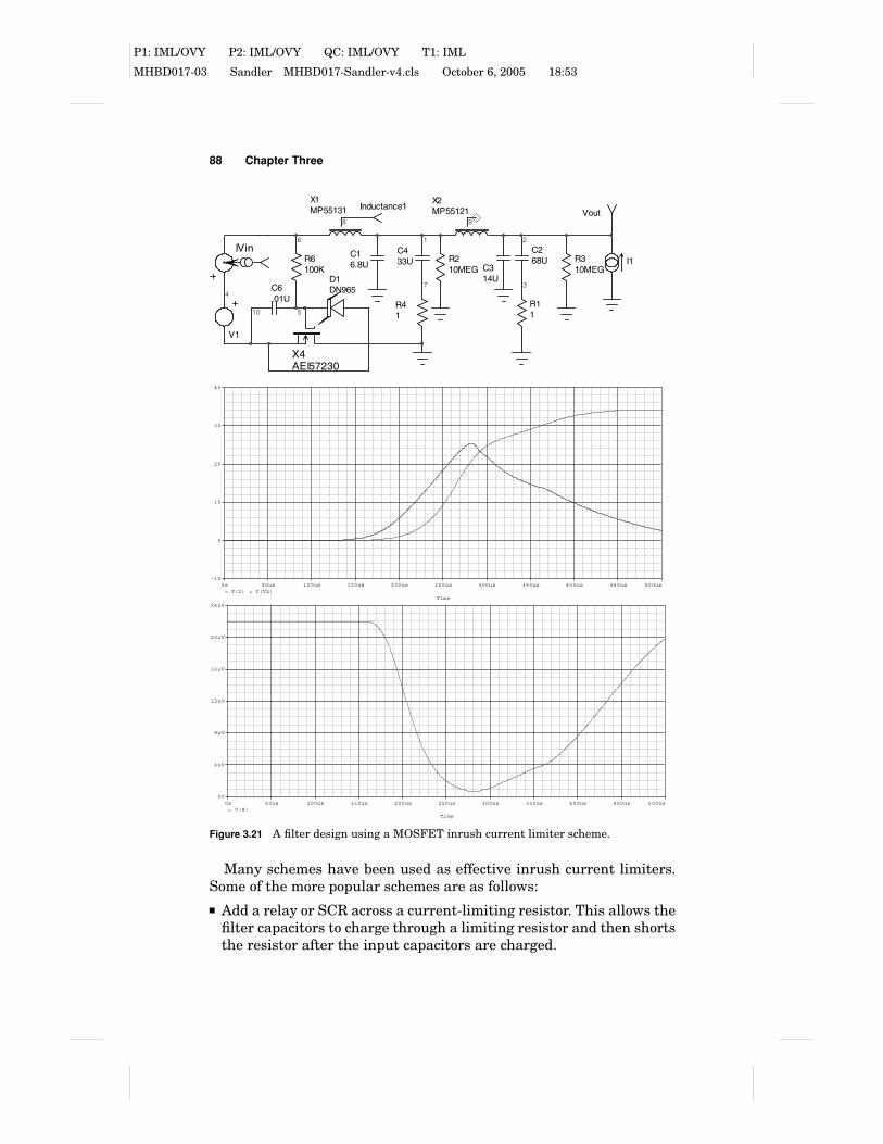
Figure 3.21 A filter design using a MOSFET inrush current limiter scheme.
Many schemes have been used as effective inrush current limiters.Some of the more popular schemes are as follows:
� Add a relay or SCR across a current-limiting resistor. This allows thefilter capacitors to charge through a limiting resistor and then shortsthe resistor after the input capacitors are charged.

P1: IML/OVY P2: IML/OVY QC: IML/OVY T1: IML
MHBD017-03 Sandler MHBD017-Sandler-v4.cls October 6, 2005 18:53
EMI Filter Design 89
� Solid-state devices such as MOSFETs can be used to limit the inputfilter’s dv/dt in order to limit the current.
� Use resistors with a negative temperature coefficient. These devicesare commercially available and provide a limiting resistance at turn-on. Once they are loaded, the resistors heat up and drastically reducein value.
As a final example, let us simulate an inrush current limiting scheme.The following schematic shows the addition of a MOSFET inrush lim-iter. The zener diode limits the gate voltage to 15 V, which is well belowthe 20-V rating. If the zener were not present, the gate voltage wouldcharge to the input voltage and damage the MOSFET.
INRSHLMT.cir.PROBE.TRAN 1u 500u 0 .5uC2 2 3 68UC3 2 0 14UR1 3 0 1C4 1 7 33UR2 1 0 10MEGR3 2 0 10MEGC6 5 10 .01UR4 7 0 1R6 6 5 100KI1 0 2 AC=1X1 6 1 8 MP55131 {N=29 DCR=.035 IC=0}X2 1 2 9 MP55121{N=36 DCR=.035 IC=0}V1 4 10 PULSE 0 32V2 4 6C1 1 0 6.8U.END
The waveforms show the inrush current with the addition of the MOS-FET limiter. Different values of R6 and C6 will produce different results;however, this is adequate in order to demonstrate the concept. The se-lected MOSFET has an Rdson that limits the power dissipation to anacceptable value.
Other implementations of inrush current limiting use negative tem-perature coefficient (NTC) thermistors designed specifically for this ap-plication. Resistor inrush limiters, which are bypassed using an SCR ora relay after the initial inrush, are also fairly common. In this case it isimportant to assure that the load on the filter is not applied until afterthe bypass device is enabled; otherwise, the input filter may not fullycharge, resulting in a second inrush when the bypass device is enabled.

P1: IML/OVY P2: IML/OVY QC: IML/OVY T1: IML
MHBD017-03 Sandler MHBD017-Sandler-v4.cls October 6, 2005 18:53
90