EMC2112 - RPM-Based Linear Fan Controller with...
65
SMSC EMC2112 DATASHEET Revision 0.88 (11-20-09) Datasheet PRODUCT FEATURES EMC2112 RPM-Based Linear Fan Controller with Hardware Thermal Shutdown General Description The EMC2112 is an SMBus, closed-loop, RPM-based fan driver with hardware (HW) thermal shutdown and reset controller. The EMC2112 offers a single High Side fan driver capable of sourcing up to 600mA from a 5V supply. The EMC2112 utilizes Beta Compensation (an implementation of the BJT or transistor model for thermal diodes) and Resistance Error Correction (REC) to accurately monitor up to three (3) external temperature zones. These features allow great accuracy for CPU substrate thermal diodes on multiple process geometries as well as with discrete diode-connected transistors. Both Beta Compensation and REC can be disabled on the EMC2112 to maintain accuracy when monitoring AMD thermal diodes. The EMC2112 provides a stand-alone HW thermal shutdown block. The HW thermal shutdown logic can be configured for a few common configurations based on the strapping level of the SHDN_SEL pin on the PCB. The HW thermal shutdown point can be set in 1°C increments by using a discrete resistor connected to the TRIP_SET pin. The EMC2112 also provides 5V supply ‘power good’ function with a threshold of 4.5V. This function is provided on the RESET pin. Applications Notebook Computers Desktop Computers Embedded Applications Features Closed-Loop RPM-Based Fan Controller — 1% accuracy with external clock input — 3% accuracy with internal clock — Internal clock can be used as a source — Aging fan detection Integrated Linear Fan Driver — 600mA drive capability HW Thermal Shutdown (SYS_SHDN ) — 1°C incremental set points for thermal shutdown — Cannot be disabled by software Provides Reset Function (RESET ) On 5V Supply Up to Three (3) Remote Thermal Zones — ±1°C accuracy (60°C to 100°C) — 0.125°C resolution — Designed to support 45nm, 65nm, and 90nm CPU Diodes using BJT and transistor model — Eliminates temperature offset due to series resistance from PCB traces and thermal ‘Diode’ Operates From Single 3.0 - 3.6V Supply — 5V supply for linear fan driver and reset generator SMBus 2.0 and I 2 C compatible — User selectable SMBus address using pull-up resistor on ADDR_SEL pin — Supports Block Read and Write functionality Available in 20-pin, 4x4 QFN Lead-free RoHS Compliant package
Transcript of EMC2112 - RPM-Based Linear Fan Controller with...
SMSC EMC2112 DATASHE
PRODUCT FEATURES
EMC2112
RPM-Based Linear Fan Controller with Hardware Thermal Shutdown
Datasheet
General DescriptionThe EMC2112 is an SMBus, closed-loop, RPM-basedfan driver with hardware (HW) thermal shutdown andreset controller. The EMC2112 offers a single High Sidefan driver capable of sourcing up to 600mA from a 5Vsupply.The EMC2112 uti l izes Beta Compensation (animplementation of the BJT or transistor model forthermal diodes) and Resistance Error Correction (REC)to accurately monitor up to three (3) externaltemperature zones. These features allow great accuracyfor CPU substrate thermal diodes on multiple processgeometries as well as with discrete diode-connectedtransistors. Both Beta Compensation and REC can bedisabled on the EMC2112 to maintain accuracy whenmonitoring AMD thermal diodes.
The EMC2112 provides a stand-alone HW thermalshutdown block. The HW thermal shutdown logic can beconfigured for a few common configurations based onthe strapping level of the SHDN_SEL pin on the PCB.The HW thermal shutdown point can be set in 1°Cincrements by using a discrete resistor connected to theTRIP_SET pin.
The EMC2112 also provides 5V supply ‘power good’function with a threshold of 4.5V. This function isprovided on the RESET pin.
ApplicationsNotebook ComputersDesktop ComputersEmbedded Applications
FeaturesClosed-Loop RPM-Based Fan Controller— 1% accuracy with external clock input— 3% accuracy with internal clock— Internal clock can be used as a source— Aging fan detectionIntegrated Linear Fan Driver— 600mA drive capabilityHW Thermal Shutdown (SYS_SHDN)— 1°C incremental set points for thermal shutdown— Cannot be disabled by softwareProvides Reset Function (RESET) On 5V SupplyUp to Three (3) Remote Thermal Zones— ±1°C accuracy (60°C to 100°C)— 0.125°C resolution— Designed to support 45nm, 65nm, and 90nm CPU
Diodes using BJT and transistor model— Eliminates temperature offset due to series resistance
from PCB traces and thermal ‘Diode’Operates From Single 3.0 - 3.6V Supply— 5V supply for linear fan driver and reset generatorSMBus 2.0 and I2C compatible— User selectable SMBus address using pull-up resistor
on ADDR_SEL pin— Supports Block Read and Write functionalityAvailable in 20-pin, 4x4 QFN Lead-free RoHS Compliant package
ET Revision 0.88 (11-20-09)

RPM-Based Linear Fan Controller with Hardware Thermal Shutdown
Datasheet
CCcrbrvkddtt
SFODTT
ORDERING INFORMATION:
Revision 0.88 (11-20-09) 2 SMSC EMC2112DATASHEET
opyright © 2009 SMSC or its subsidiaries. All rights reserved.ircuit diagrams and other information relating to SMSC products are included as a means of illustrating typical applications. Consequently, complete information sufficient foronstruction purposes is not necessarily given. Although the information has been checked and is believed to be accurate, no responsibility is assumed for inaccuracies. SMSCeserves the right to make changes to specifications and product descriptions at any time without notice. Contact your local SMSC sales office to obtain the latest specificationsefore placing your product order. The provision of this information does not convey to the purchaser of the described semiconductor devices any licenses under any patentights or other intellectual property rights of SMSC or others. All sales are expressly conditional on your agreement to the terms and conditions of the most recently datedersion of SMSC's standard Terms of Sale Agreement dated before the date of your order (the "Terms of Sale Agreement"). The product may contain design defects or errorsnown as anomalies which may cause the product's functions to deviate from published specifications. Anomaly sheets are available upon request. SMSC products are notesigned, intended, authorized or warranted for use in any life support or other application where product failure could cause or contribute to personal injury or severe propertyamage. Any and all such uses without prior written approval of an Officer of SMSC and further testing and/or modification will be fully at the risk of the customer. Copies ofhis document or other SMSC literature, as well as the Terms of Sale Agreement, may be obtained by visiting SMSC’s website at http://www.smsc.com. SMSC is a registeredrademark of Standard Microsystems Corporation (“SMSC”). Product names and company names are the trademarks of their respective holders.
MSC DISCLAIMS AND EXCLUDES ANY AND ALL WARRANTIES, INCLUDING WITHOUT LIMITATION ANY AND ALL IMPLIED WARRANTIES OF MERCHANTABILITY,ITNESS FOR A PARTICULAR PURPOSE, TITLE, AND AGAINST INFRINGEMENT AND THE LIKE, AND ANY AND ALL WARRANTIES ARISING FROM ANY COURSEF DEALING OR USAGE OF TRADE. IN NO EVENT SHALL SMSC BE LIABLE FOR ANY DIRECT, INCIDENTAL, INDIRECT, SPECIAL, PUNITIVE, OR CONSEQUENTIALAMAGES; OR FOR LOST DATA, PROFITS, SAVINGS OR REVENUES OF ANY KIND; REGARDLESS OF THE FORM OF ACTION, WHETHER BASED ON CONTRACT;ORT; NEGLIGENCE OF SMSC OR OTHERS; STRICT LIABILITY; BREACH OF WARRANTY; OR OTHERWISE; WHETHER OR NOT ANY REMEDY OF BUYER IS HELDO HAVE FAILED OF ITS ESSENTIAL PURPOSE, AND WHETHER OR NOT SMSC HAS BEEN ADVISED OF THE POSSIBILITY OF SUCH DAMAGES.
REEL SIZE IS 4,000 PIECES
This product meets the halogen maximum concentration values per IEC61249-2-21
For RoHS compliance and environmental information, please visit www.smsc.com/rohs
Please contact your SMSC sales representative for additional documentation related to this product such as application notes, anomaly sheets, and design guidelines.
ORDERING NUMBER PACKAGE FEATURES
EMC2112-BP-TR 20-pin QFN 4mm x 4mm (Lead-Free RoHS compliant)
Three External Diodes. High Side Fan driver w/ RPM based Fan Speed Control algorithm. Reset generator. Hardware set critical temperature limit
RPM-Based Linear Fan Controller with Hardware Thermal Shutdown
Datasheet
Table of Contents
Chapter 1 Block Diagram . . . . . . . . . . . . . . . . . . . . . . . . . . . . . . . . . . . . . . . . . . . . . . . . . . . . . 8
Chapter 2 Pin Layout . . . . . . . . . . . . . . . . . . . . . . . . . . . . . . . . . . . . . . . . . . . . . . . . . . . . . . . . 92.1 Pin Layout for EMC2112. . . . . . . . . . . . . . . . . . . . . . . . . . . . . . . . . . . . . . . . . . . . . . . . . . . . . . . . . . 92.2 Pin Description for EMC2112 . . . . . . . . . . . . . . . . . . . . . . . . . . . . . . . . . . . . . . . . . . . . . . . . . . . . . . 9
Chapter 3 Electrical Specifications . . . . . . . . . . . . . . . . . . . . . . . . . . . . . . . . . . . . . . . . . . . . 123.1 Absolute Maximum Ratings . . . . . . . . . . . . . . . . . . . . . . . . . . . . . . . . . . . . . . . . . . . . . . . . . . . . . . 123.2 Electrical Specifications . . . . . . . . . . . . . . . . . . . . . . . . . . . . . . . . . . . . . . . . . . . . . . . . . . . . . . . . . 123.3 SMBus Electrical Specifications . . . . . . . . . . . . . . . . . . . . . . . . . . . . . . . . . . . . . . . . . . . . . . . . . . . 14
Chapter 4 System Management Bus Interface Protocol . . . . . . . . . . . . . . . . . . . . . . . . . . . 164.1 System Management Bus Interface Protocol . . . . . . . . . . . . . . . . . . . . . . . . . . . . . . . . . . . . . . . . . 16
4.1.1 SMBus Start Bit . . . . . . . . . . . . . . . . . . . . . . . . . . . . . . . . . . . . . . . . . . . . . . . . . . . . . . . . 164.1.2 SMBus Address and RD / WR Bit . . . . . . . . . . . . . . . . . . . . . . . . . . . . . . . . . . . . . . . . . . 164.1.3 SMBus Data Bytes . . . . . . . . . . . . . . . . . . . . . . . . . . . . . . . . . . . . . . . . . . . . . . . . . . . . . 174.1.4 SMBus ACK and NACK Bits . . . . . . . . . . . . . . . . . . . . . . . . . . . . . . . . . . . . . . . . . . . . . . 174.1.5 SMBus Stop Bit . . . . . . . . . . . . . . . . . . . . . . . . . . . . . . . . . . . . . . . . . . . . . . . . . . . . . . . . 174.1.6 SMBus Time-out . . . . . . . . . . . . . . . . . . . . . . . . . . . . . . . . . . . . . . . . . . . . . . . . . . . . . . . 174.1.7 SMBus and I2C Compliance . . . . . . . . . . . . . . . . . . . . . . . . . . . . . . . . . . . . . . . . . . . . . . 17
4.2 SMBus Protocols . . . . . . . . . . . . . . . . . . . . . . . . . . . . . . . . . . . . . . . . . . . . . . . . . . . . . . . . . . . . . . 174.2.1 Write Byte . . . . . . . . . . . . . . . . . . . . . . . . . . . . . . . . . . . . . . . . . . . . . . . . . . . . . . . . . . . . 184.2.2 Read Byte . . . . . . . . . . . . . . . . . . . . . . . . . . . . . . . . . . . . . . . . . . . . . . . . . . . . . . . . . . . . 184.2.3 Send Byte . . . . . . . . . . . . . . . . . . . . . . . . . . . . . . . . . . . . . . . . . . . . . . . . . . . . . . . . . . . . 184.2.4 Receive Byte . . . . . . . . . . . . . . . . . . . . . . . . . . . . . . . . . . . . . . . . . . . . . . . . . . . . . . . . . . 184.2.5 Block Write Protocol . . . . . . . . . . . . . . . . . . . . . . . . . . . . . . . . . . . . . . . . . . . . . . . . . . . . 194.2.6 Block Read Protocol . . . . . . . . . . . . . . . . . . . . . . . . . . . . . . . . . . . . . . . . . . . . . . . . . . . . 194.2.7 Alert Response Address . . . . . . . . . . . . . . . . . . . . . . . . . . . . . . . . . . . . . . . . . . . . . . . . . 19
Chapter 5 General Description. . . . . . . . . . . . . . . . . . . . . . . . . . . . . . . . . . . . . . . . . . . . . . . . 205.1 Fan Control Modes of Operation . . . . . . . . . . . . . . . . . . . . . . . . . . . . . . . . . . . . . . . . . . . . . . . . . . 215.2 RPM-Based Fan Speed Control Algorithm (FSC) . . . . . . . . . . . . . . . . . . . . . . . . . . . . . . . . . . . . . 21
5.2.1 Programming the RPM-Based Fan Speed Control Algorithm . . . . . . . . . . . . . . . . . . . . . 225.3 Tachometer Measurement . . . . . . . . . . . . . . . . . . . . . . . . . . . . . . . . . . . . . . . . . . . . . . . . . . . . . . . 22
5.3.1 Stalled Fan . . . . . . . . . . . . . . . . . . . . . . . . . . . . . . . . . . . . . . . . . . . . . . . . . . . . . . . . . . . 225.3.2 Aging Fan or Invalid Drive Detection . . . . . . . . . . . . . . . . . . . . . . . . . . . . . . . . . . . . . . . . 235.3.3 Clock Source . . . . . . . . . . . . . . . . . . . . . . . . . . . . . . . . . . . . . . . . . . . . . . . . . . . . . . . . . . 23
5.4 Spin Up Routine . . . . . . . . . . . . . . . . . . . . . . . . . . . . . . . . . . . . . . . . . . . . . . . . . . . . . . . . . . . . . . . 235.5 Ramp Rate Control . . . . . . . . . . . . . . . . . . . . . . . . . . . . . . . . . . . . . . . . . . . . . . . . . . . . . . . . . . . . . 24
5.5.1 Temperature Bypass of Ramp Rate Control . . . . . . . . . . . . . . . . . . . . . . . . . . . . . . . . . . 255.6 Watchdog Timer . . . . . . . . . . . . . . . . . . . . . . . . . . . . . . . . . . . . . . . . . . . . . . . . . . . . . . . . . . . . . . . 25
5.6.1 Power Up Operation . . . . . . . . . . . . . . . . . . . . . . . . . . . . . . . . . . . . . . . . . . . . . . . . . . . . 265.6.2 Continuous Operation . . . . . . . . . . . . . . . . . . . . . . . . . . . . . . . . . . . . . . . . . . . . . . . . . . . 26
5.7 High Side Fan Driver . . . . . . . . . . . . . . . . . . . . . . . . . . . . . . . . . . . . . . . . . . . . . . . . . . . . . . . . . . . 265.7.1 Overcurrent Limit . . . . . . . . . . . . . . . . . . . . . . . . . . . . . . . . . . . . . . . . . . . . . . . . . . . . . . . 26
5.8 Internal Thermal Shutdown (TSD) . . . . . . . . . . . . . . . . . . . . . . . . . . . . . . . . . . . . . . . . . . . . . . . . . 265.9 Critical/Thermal Shutdown . . . . . . . . . . . . . . . . . . . . . . . . . . . . . . . . . . . . . . . . . . . . . . . . . . . . . . . 26
5.9.1 TRIP_SET Pin . . . . . . . . . . . . . . . . . . . . . . . . . . . . . . . . . . . . . . . . . . . . . . . . . . . . . . . . . 275.9.2 SHDN_SEL Pin . . . . . . . . . . . . . . . . . . . . . . . . . . . . . . . . . . . . . . . . . . . . . . . . . . . . . . . . 295.9.3 Internal HW_SHDN Signal . . . . . . . . . . . . . . . . . . . . . . . . . . . . . . . . . . . . . . . . . . . . . . . 29
5.10 5V Reset Controller . . . . . . . . . . . . . . . . . . . . . . . . . . . . . . . . . . . . . . . . . . . . . . . . . . . . . . . . . . . . 30
SMSC EMC2112 3 Revision 0.88 (11-20-09)DATASHEET
RPM-Based Linear Fan Controller with Hardware Thermal Shutdown
Datasheet
5.11 Temperature Monitoring . . . . . . . . . . . . . . . . . . . . . . . . . . . . . . . . . . . . . . . . . . . . . . . . . . . . . . . . . 305.11.1 Dynamic Averaging . . . . . . . . . . . . . . . . . . . . . . . . . . . . . . . . . . . . . . . . . . . . . . . . . . . . . 315.11.2 Resistance Error Correction . . . . . . . . . . . . . . . . . . . . . . . . . . . . . . . . . . . . . . . . . . . . . . 315.11.3 Beta Compensation . . . . . . . . . . . . . . . . . . . . . . . . . . . . . . . . . . . . . . . . . . . . . . . . . . . . . 315.11.4 Digital Averaging . . . . . . . . . . . . . . . . . . . . . . . . . . . . . . . . . . . . . . . . . . . . . . . . . . . . . . . 32
5.12 Diode Connections . . . . . . . . . . . . . . . . . . . . . . . . . . . . . . . . . . . . . . . . . . . . . . . . . . . . . . . . . . . . . 325.12.1 Diode Faults . . . . . . . . . . . . . . . . . . . . . . . . . . . . . . . . . . . . . . . . . . . . . . . . . . . . . . . . . . 32
Chapter 6 Register Set . . . . . . . . . . . . . . . . . . . . . . . . . . . . . . . . . . . . . . . . . . . . . . . . . . . . . . . 336.1 Register Map . . . . . . . . . . . . . . . . . . . . . . . . . . . . . . . . . . . . . . . . . . . . . . . . . . . . . . . . . . . . . . . . . 33
6.1.1 Lock Entries. . . . . . . . . . . . . . . . . . . . . . . . . . . . . . . . . . . . . . . . . . . . . . . . . . . . . . . . . . . 366.2 Temperature Data Registers . . . . . . . . . . . . . . . . . . . . . . . . . . . . . . . . . . . . . . . . . . . . . . . . . . . . . 366.3 Critical/Thermal Shutdown Temperature Registers . . . . . . . . . . . . . . . . . . . . . . . . . . . . . . . . . . . . 376.4 TripSet Voltage Register. . . . . . . . . . . . . . . . . . . . . . . . . . . . . . . . . . . . . . . . . . . . . . . . . . . . . . . . . 386.5 Ideality Factor Registers . . . . . . . . . . . . . . . . . . . . . . . . . . . . . . . . . . . . . . . . . . . . . . . . . . . . . . . . . 386.6 Beta Configuration Registers . . . . . . . . . . . . . . . . . . . . . . . . . . . . . . . . . . . . . . . . . . . . . . . . . . . . . 396.7 REC Configuration Register . . . . . . . . . . . . . . . . . . . . . . . . . . . . . . . . . . . . . . . . . . . . . . . . . . . . . . 416.8 Critical Temperature Limit Registers . . . . . . . . . . . . . . . . . . . . . . . . . . . . . . . . . . . . . . . . . . . . . . . 416.9 Configuration Register . . . . . . . . . . . . . . . . . . . . . . . . . . . . . . . . . . . . . . . . . . . . . . . . . . . . . . . . . . 426.10 Configuration 2 Register . . . . . . . . . . . . . . . . . . . . . . . . . . . . . . . . . . . . . . . . . . . . . . . . . . . . . . . . . 436.11 Interrupt Status Register. . . . . . . . . . . . . . . . . . . . . . . . . . . . . . . . . . . . . . . . . . . . . . . . . . . . . . . . . 446.12 Error Status Registers . . . . . . . . . . . . . . . . . . . . . . . . . . . . . . . . . . . . . . . . . . . . . . . . . . . . . . . . . . 45
6.12.1 Tcrit Status Register . . . . . . . . . . . . . . . . . . . . . . . . . . . . . . . . . . . . . . . . . . . . . . . . . . . . 456.13 Fan Status Register . . . . . . . . . . . . . . . . . . . . . . . . . . . . . . . . . . . . . . . . . . . . . . . . . . . . . . . . . . . . 466.14 Interrupt Enable Register . . . . . . . . . . . . . . . . . . . . . . . . . . . . . . . . . . . . . . . . . . . . . . . . . . . . . . . . 466.15 Fan Interrupt Enable Register. . . . . . . . . . . . . . . . . . . . . . . . . . . . . . . . . . . . . . . . . . . . . . . . . . . . . 476.16 Limit Registers . . . . . . . . . . . . . . . . . . . . . . . . . . . . . . . . . . . . . . . . . . . . . . . . . . . . . . . . . . . . . . . . 476.17 Fan Setting Register . . . . . . . . . . . . . . . . . . . . . . . . . . . . . . . . . . . . . . . . . . . . . . . . . . . . . . . . . . . . 486.18 Fan Configuration 1 Register . . . . . . . . . . . . . . . . . . . . . . . . . . . . . . . . . . . . . . . . . . . . . . . . . . . . . 486.19 Fan Configuration 2 Register . . . . . . . . . . . . . . . . . . . . . . . . . . . . . . . . . . . . . . . . . . . . . . . . . . . . . 506.20 Gain Register . . . . . . . . . . . . . . . . . . . . . . . . . . . . . . . . . . . . . . . . . . . . . . . . . . . . . . . . . . . . . . . . . 516.21 Fan Spin Up Configuration Register . . . . . . . . . . . . . . . . . . . . . . . . . . . . . . . . . . . . . . . . . . . . . . . . 526.22 Fan Max Step Register . . . . . . . . . . . . . . . . . . . . . . . . . . . . . . . . . . . . . . . . . . . . . . . . . . . . . . . . . . 536.23 Fan Minimum Drive Register . . . . . . . . . . . . . . . . . . . . . . . . . . . . . . . . . . . . . . . . . . . . . . . . . . . . . 546.24 Valid TACH Count Register . . . . . . . . . . . . . . . . . . . . . . . . . . . . . . . . . . . . . . . . . . . . . . . . . . . . . . 546.25 Fan Drive Fail Band Registers . . . . . . . . . . . . . . . . . . . . . . . . . . . . . . . . . . . . . . . . . . . . . . . . . . . . 556.26 TACH Target Registers . . . . . . . . . . . . . . . . . . . . . . . . . . . . . . . . . . . . . . . . . . . . . . . . . . . . . . . . . 556.27 TACH Reading Registers . . . . . . . . . . . . . . . . . . . . . . . . . . . . . . . . . . . . . . . . . . . . . . . . . . . . . . . . 556.28 Software Lock Register. . . . . . . . . . . . . . . . . . . . . . . . . . . . . . . . . . . . . . . . . . . . . . . . . . . . . . . . . . 566.29 Product Features Register . . . . . . . . . . . . . . . . . . . . . . . . . . . . . . . . . . . . . . . . . . . . . . . . . . . . . . . 576.30 Product ID Register . . . . . . . . . . . . . . . . . . . . . . . . . . . . . . . . . . . . . . . . . . . . . . . . . . . . . . . . . . . . 576.31 Manufacturer ID Register . . . . . . . . . . . . . . . . . . . . . . . . . . . . . . . . . . . . . . . . . . . . . . . . . . . . . . . . 586.32 Revision Register . . . . . . . . . . . . . . . . . . . . . . . . . . . . . . . . . . . . . . . . . . . . . . . . . . . . . . . . . . . . . . 58
Chapter 7 Typical Operating Curves. . . . . . . . . . . . . . . . . . . . . . . . . . . . . . . . . . . . . . . . . . . 59
Chapter 8 Package Outline . . . . . . . . . . . . . . . . . . . . . . . . . . . . . . . . . . . . . . . . . . . . . . . . . . . 628.1 EMC2112 Package Drawings - 20-Pin QFN 4mm x 4mm . . . . . . . . . . . . . . . . . . . . . . . . . . . . . . . 628.2 Package Marking Information . . . . . . . . . . . . . . . . . . . . . . . . . . . . . . . . . . . . . . . . . . . . . . . . . . . . . 64
Chapter 9 Datasheet Revision History . . . . . . . . . . . . . . . . . . . . . . . . . . . . . . . . . . . . . . . . . . 65
Revision 0.88 (11-20-09) 4 SMSC EMC2112DATASHEET
RPM-Based Linear Fan Controller with Hardware Thermal Shutdown
Datasheet
SMSC EMC2112 5 Revision 0.88 (11-20-09)DATASHEET
List of FiguresFigure 1.1 EMC2112 Block Diagram. . . . . . . . . . . . . . . . . . . . . . . . . . . . . . . . . . . . . . . . . . . . . . . . . . . . . 8Figure 2.1 EMC2112 Pin Diagram . . . . . . . . . . . . . . . . . . . . . . . . . . . . . . . . . . . . . . . . . . . . . . . . . . . . . . 9Figure 4.1 SMBus Timing Diagram . . . . . . . . . . . . . . . . . . . . . . . . . . . . . . . . . . . . . . . . . . . . . . . . . . . . . 16Figure 5.1 EMC2112 System Diagram . . . . . . . . . . . . . . . . . . . . . . . . . . . . . . . . . . . . . . . . . . . . . . . . . . 20Figure 5.2 Spin Up Routine . . . . . . . . . . . . . . . . . . . . . . . . . . . . . . . . . . . . . . . . . . . . . . . . . . . . . . . . . . . 24Figure 5.3 Ramp Rate Control . . . . . . . . . . . . . . . . . . . . . . . . . . . . . . . . . . . . . . . . . . . . . . . . . . . . . . . . 25Figure 5.4 EMC2112 Critical/Thermal Shutdown Block Diagram . . . . . . . . . . . . . . . . . . . . . . . . . . . . . . 27Figure 5.5 HW_SHDN Operation . . . . . . . . . . . . . . . . . . . . . . . . . . . . . . . . . . . . . . . . . . . . . . . . . . . . . . 30Figure 5.6 5V Reset Controller Timing . . . . . . . . . . . . . . . . . . . . . . . . . . . . . . . . . . . . . . . . . . . . . . . . . . 30Figure 5.7 Diode Connections. . . . . . . . . . . . . . . . . . . . . . . . . . . . . . . . . . . . . . . . . . . . . . . . . . . . . . . . . 32Figure 8.1 EMC2112 Package Drawing - 20-Pin QFN 4mm x 4mm. . . . . . . . . . . . . . . . . . . . . . . . . . . . 62Figure 8.2 EMC2112 Package Dimensions and Notes - 20-Pin QFN 4mm x 4mm . . . . . . . . . . . . . . . . 63Figure 8.3 EMC2112 PCB Footprint - 20-Pin QFN 4mm x 4mm. . . . . . . . . . . . . . . . . . . . . . . . . . . . . . . 63Figure 8.4 EMC2112 Package Markings. . . . . . . . . . . . . . . . . . . . . . . . . . . . . . . . . . . . . . . . . . . . . . . . . 64

RPM-Based Linear Fan Controller with Hardware Thermal Shutdown
Datasheet
List of TablesTable 2.1 Pin Description. . . . . . . . . . . . . . . . . . . . . . . . . . . . . . . . . . . . . . . . . . . . . . . . . . . . . . . . . . . . . . 9Table 2.2 Pin Types. . . . . . . . . . . . . . . . . . . . . . . . . . . . . . . . . . . . . . . . . . . . . . . . . . . . . . . . . . . . . . . . . 10Table 3.1 Absolute Maximum Ratings . . . . . . . . . . . . . . . . . . . . . . . . . . . . . . . . . . . . . . . . . . . . . . . . . . . 12Table 3.2 Electrical Specifications . . . . . . . . . . . . . . . . . . . . . . . . . . . . . . . . . . . . . . . . . . . . . . . . . . . . . . 12Table 3.3 SMBus Electrical Specifications . . . . . . . . . . . . . . . . . . . . . . . . . . . . . . . . . . . . . . . . . . . . . . . 14Table 4.1 ADDR_SEL Pin Configuration . . . . . . . . . . . . . . . . . . . . . . . . . . . . . . . . . . . . . . . . . . . . . . . . . 16Table 4.2 Protocol Format . . . . . . . . . . . . . . . . . . . . . . . . . . . . . . . . . . . . . . . . . . . . . . . . . . . . . . . . . . . . 17Table 4.3 Write Byte Protocol . . . . . . . . . . . . . . . . . . . . . . . . . . . . . . . . . . . . . . . . . . . . . . . . . . . . . . . . . 18Table 4.4 Read Byte Protocol . . . . . . . . . . . . . . . . . . . . . . . . . . . . . . . . . . . . . . . . . . . . . . . . . . . . . . . . . 18Table 4.5 Send Byte Protocol . . . . . . . . . . . . . . . . . . . . . . . . . . . . . . . . . . . . . . . . . . . . . . . . . . . . . . . . . 18Table 4.6 Receive Byte Protocol . . . . . . . . . . . . . . . . . . . . . . . . . . . . . . . . . . . . . . . . . . . . . . . . . . . . . . . 18Table 4.7 Block Write Protocol . . . . . . . . . . . . . . . . . . . . . . . . . . . . . . . . . . . . . . . . . . . . . . . . . . . . . . . . 19Table 4.8 Block Read Protocol . . . . . . . . . . . . . . . . . . . . . . . . . . . . . . . . . . . . . . . . . . . . . . . . . . . . . . . . 19Table 4.9 Alert Response Address Protocol . . . . . . . . . . . . . . . . . . . . . . . . . . . . . . . . . . . . . . . . . . . . . . 19Table 5.1 Fan Controls Active for Operating Mode . . . . . . . . . . . . . . . . . . . . . . . . . . . . . . . . . . . . . . . . . 21Table 5.2 TRIP_SET Resistor Setting . . . . . . . . . . . . . . . . . . . . . . . . . . . . . . . . . . . . . . . . . . . . . . . . . . . 28Table 5.3 SHDN_SEL Pin Configuration . . . . . . . . . . . . . . . . . . . . . . . . . . . . . . . . . . . . . . . . . . . . . . . . . 29Table 5.4 Dynamic Averaging Behavior . . . . . . . . . . . . . . . . . . . . . . . . . . . . . . . . . . . . . . . . . . . . . . . . . 31Table 6.1 EMC2112 Register Set . . . . . . . . . . . . . . . . . . . . . . . . . . . . . . . . . . . . . . . . . . . . . . . . . . . . . . 33Table 6.2 Temperature Data Registers . . . . . . . . . . . . . . . . . . . . . . . . . . . . . . . . . . . . . . . . . . . . . . . . . . 36Table 6.3 Temperature Data Format . . . . . . . . . . . . . . . . . . . . . . . . . . . . . . . . . . . . . . . . . . . . . . . . . . . . 37Table 6.4 Critical/Thermal Shutdown Temperature Registers. . . . . . . . . . . . . . . . . . . . . . . . . . . . . . . . . 37Table 6.5 Critical / Thermal Shutdown Data Format . . . . . . . . . . . . . . . . . . . . . . . . . . . . . . . . . . . . . . . . 37Table 6.6 TripSet Voltage Register . . . . . . . . . . . . . . . . . . . . . . . . . . . . . . . . . . . . . . . . . . . . . . . . . . . . . 38Table 6.7 Ideality Factor Registers . . . . . . . . . . . . . . . . . . . . . . . . . . . . . . . . . . . . . . . . . . . . . . . . . . . . . 38Table 6.8 Ideality Factor Look-Up Table . . . . . . . . . . . . . . . . . . . . . . . . . . . . . . . . . . . . . . . . . . . . . . . . . 39Table 6.9 Substrate Diode Ideality Factor Look-Up Table (BJT Model) . . . . . . . . . . . . . . . . . . . . . . . . . 39Table 6.10 Beta Configuration Registers. . . . . . . . . . . . . . . . . . . . . . . . . . . . . . . . . . . . . . . . . . . . . . . . . . 39Table 6.11 Beta Compensation . . . . . . . . . . . . . . . . . . . . . . . . . . . . . . . . . . . . . . . . . . . . . . . . . . . . . . . . . 40Table 6.12 REC Configuration Register . . . . . . . . . . . . . . . . . . . . . . . . . . . . . . . . . . . . . . . . . . . . . . . . . . 41Table 6.13 Tcrit Limit Registers . . . . . . . . . . . . . . . . . . . . . . . . . . . . . . . . . . . . . . . . . . . . . . . . . . . . . . . . 41Table 6.14 Configuration Register . . . . . . . . . . . . . . . . . . . . . . . . . . . . . . . . . . . . . . . . . . . . . . . . . . . . . . . 42Table 6.15 Configuration 2 Register . . . . . . . . . . . . . . . . . . . . . . . . . . . . . . . . . . . . . . . . . . . . . . . . . . . . . 43Table 6.16 Fault Queue . . . . . . . . . . . . . . . . . . . . . . . . . . . . . . . . . . . . . . . . . . . . . . . . . . . . . . . . . . . . . . . 44Table 6.17 Conversion Rate . . . . . . . . . . . . . . . . . . . . . . . . . . . . . . . . . . . . . . . . . . . . . . . . . . . . . . . . . . . 44Table 6.18 Interrupt Status Register . . . . . . . . . . . . . . . . . . . . . . . . . . . . . . . . . . . . . . . . . . . . . . . . . . . . . 44Table 6.19 Error Status Register . . . . . . . . . . . . . . . . . . . . . . . . . . . . . . . . . . . . . . . . . . . . . . . . . . . . . . . . 45Table 6.20 Fan Status Register . . . . . . . . . . . . . . . . . . . . . . . . . . . . . . . . . . . . . . . . . . . . . . . . . . . . . . . . . 46Table 6.21 Interrupt Enable Register. . . . . . . . . . . . . . . . . . . . . . . . . . . . . . . . . . . . . . . . . . . . . . . . . . . . . 46Table 6.22 Fan Interrupt Enable Register. . . . . . . . . . . . . . . . . . . . . . . . . . . . . . . . . . . . . . . . . . . . . . . . . 47Table 6.23 Limit Registers . . . . . . . . . . . . . . . . . . . . . . . . . . . . . . . . . . . . . . . . . . . . . . . . . . . . . . . . . . . . 47Table 6.24 Fan Setting Register . . . . . . . . . . . . . . . . . . . . . . . . . . . . . . . . . . . . . . . . . . . . . . . . . . . . . . . . 48Table 6.25 Fan Configuration 1 Register. . . . . . . . . . . . . . . . . . . . . . . . . . . . . . . . . . . . . . . . . . . . . . . . . . 48Table 6.26 Range Decode. . . . . . . . . . . . . . . . . . . . . . . . . . . . . . . . . . . . . . . . . . . . . . . . . . . . . . . . . . . . . 49Table 6.27 Minimum Edges for Fan Rotation . . . . . . . . . . . . . . . . . . . . . . . . . . . . . . . . . . . . . . . . . . . . . . 49Table 6.28 Update Time . . . . . . . . . . . . . . . . . . . . . . . . . . . . . . . . . . . . . . . . . . . . . . . . . . . . . . . . . . . . . . 49Table 6.29 Fan Configuration 1 Register. . . . . . . . . . . . . . . . . . . . . . . . . . . . . . . . . . . . . . . . . . . . . . . . . . 50Table 6.30 Derivative Options . . . . . . . . . . . . . . . . . . . . . . . . . . . . . . . . . . . . . . . . . . . . . . . . . . . . . . . . . . 51Table 6.31 Error Range Options . . . . . . . . . . . . . . . . . . . . . . . . . . . . . . . . . . . . . . . . . . . . . . . . . . . . . . . . 51Table 6.32 Gain Register. . . . . . . . . . . . . . . . . . . . . . . . . . . . . . . . . . . . . . . . . . . . . . . . . . . . . . . . . . . . . . 51Table 6.33 Gain Decode . . . . . . . . . . . . . . . . . . . . . . . . . . . . . . . . . . . . . . . . . . . . . . . . . . . . . . . . . . . . . . 52Table 6.34 Fan Spin Up Configuration Register . . . . . . . . . . . . . . . . . . . . . . . . . . . . . . . . . . . . . . . . . . . . 52
Revision 0.88 (11-20-09) 6 SMSC EMC2112DATASHEET

RPM-Based Linear Fan Controller with Hardware Thermal Shutdown
Datasheet
Table 6.35 DRIVE_FAIL_CNT[1:0] Bit Decode . . . . . . . . . . . . . . . . . . . . . . . . . . . . . . . . . . . . . . . . . . . . . 52Table 6.36 Spin Level . . . . . . . . . . . . . . . . . . . . . . . . . . . . . . . . . . . . . . . . . . . . . . . . . . . . . . . . . . . . . . . . 53Table 6.37 Spin Time. . . . . . . . . . . . . . . . . . . . . . . . . . . . . . . . . . . . . . . . . . . . . . . . . . . . . . . . . . . . . . . . . 53Table 6.38 Fan Max Step Register . . . . . . . . . . . . . . . . . . . . . . . . . . . . . . . . . . . . . . . . . . . . . . . . . . . . . . 53Table 6.39 Minimum Fan Drive Register . . . . . . . . . . . . . . . . . . . . . . . . . . . . . . . . . . . . . . . . . . . . . . . . . . 54Table 6.40 Valid TACH Count Register . . . . . . . . . . . . . . . . . . . . . . . . . . . . . . . . . . . . . . . . . . . . . . . . . . . 54Table 6.41 Fan Drive Fail Band Registers. . . . . . . . . . . . . . . . . . . . . . . . . . . . . . . . . . . . . . . . . . . . . . . . . 55Table 6.42 TACH Target Registers . . . . . . . . . . . . . . . . . . . . . . . . . . . . . . . . . . . . . . . . . . . . . . . . . . . . . . 55Table 6.43 TACH Reading Registers . . . . . . . . . . . . . . . . . . . . . . . . . . . . . . . . . . . . . . . . . . . . . . . . . . . . 55Table 6.44 Software Lock Register . . . . . . . . . . . . . . . . . . . . . . . . . . . . . . . . . . . . . . . . . . . . . . . . . . . . . . 56Table 6.45 Product Features Register. . . . . . . . . . . . . . . . . . . . . . . . . . . . . . . . . . . . . . . . . . . . . . . . . . . . 57Table 6.46 ADDR_SEL Pin Configuration . . . . . . . . . . . . . . . . . . . . . . . . . . . . . . . . . . . . . . . . . . . . . . . . . 57Table 6.47 SHDN_CH Pin Configuration. . . . . . . . . . . . . . . . . . . . . . . . . . . . . . . . . . . . . . . . . . . . . . . . . . 57Table 6.48 Product ID Register . . . . . . . . . . . . . . . . . . . . . . . . . . . . . . . . . . . . . . . . . . . . . . . . . . . . . . . . . 57Table 6.49 Manufacturer ID Register. . . . . . . . . . . . . . . . . . . . . . . . . . . . . . . . . . . . . . . . . . . . . . . . . . . . . 58Table 6.50 Revision Register. . . . . . . . . . . . . . . . . . . . . . . . . . . . . . . . . . . . . . . . . . . . . . . . . . . . . . . . . . . 58Table 9.1 Customer Revision History . . . . . . . . . . . . . . . . . . . . . . . . . . . . . . . . . . . . . . . . . . . . . . . . . . . 65
SMSC EMC2112 7 Revision 0.88 (11-20-09)DATASHEET

RPM-Based Linear Fan Controller with Hardware Thermal Shutdown
Datasheet
Chapter 1 Block Diagram
Figure 1.1 EMC2112 Block Diagram
Analog Mux
External Temp
Diodes
Internal Temp Diode
11 bit Σ Δ ADC Ext. Temp Registers
Register Set and
Logic
DP1
SMCLK
SMDATA
Ext Temp Limit
Registers
ALERT
Voltage Reading
DN1
DP2 / DN3DN2 / DP3
TRIP_SETCritical / Thermal Shutdown Logic
High Side Fan Driver
8-bit DAC
FAN
(2)
VD
D_5
V (2
)
SMBus Slave
Protocol
SY
S_S
HD
N
Bandgap Reference
Automatic Fan Control Algorithm
TACH Monitor
Reset Generator
RES
ET
TAC
H
Voltage -> Temperature Converison
VD
D_3
V
VDD_5V
AD
DR
_SE
L
SH
DN
_SE
L
CLK
Anti-parallel Diode
Revision 0.88 (11-20-09) 8 SMSC EMC2112DATASHEET
RPM-Based Linear Fan Controller with Hardware Thermal Shutdown
Datasheet
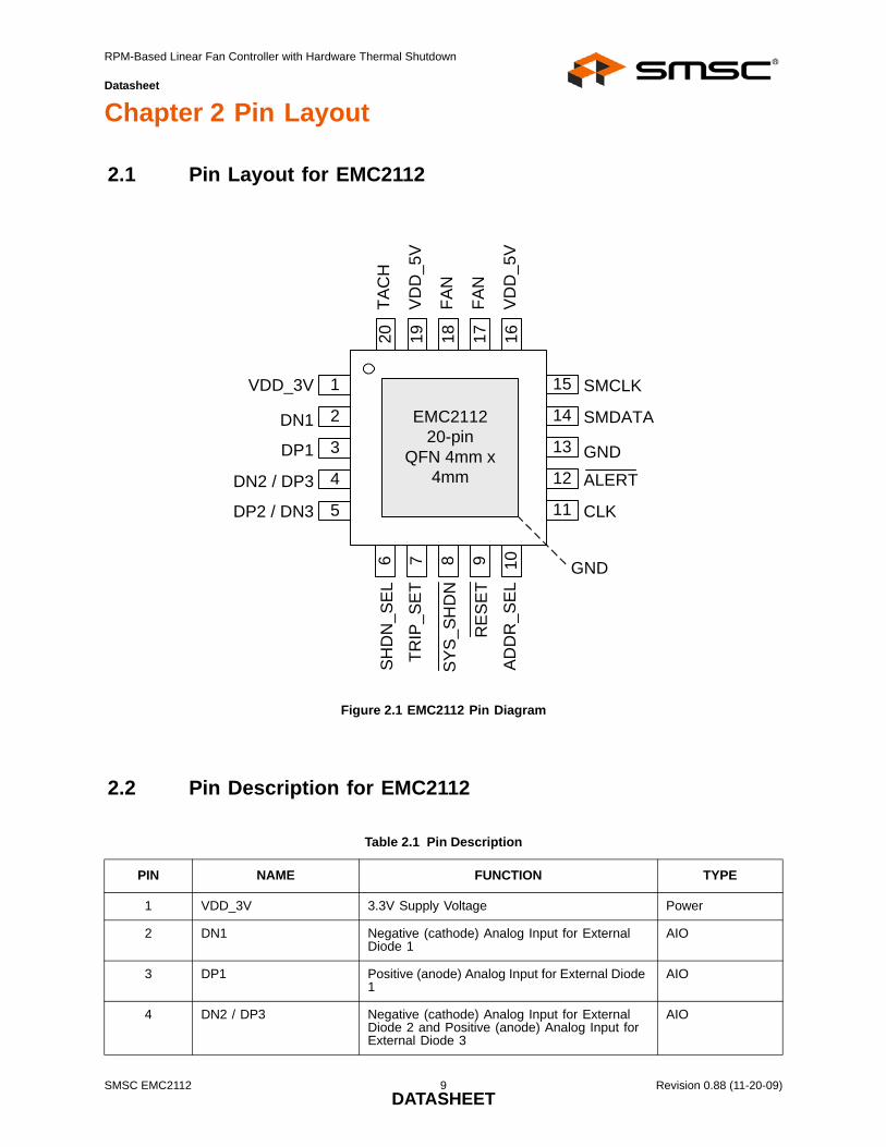
Chapter 2 Pin Layout
2.1 Pin Layout for EMC2112
2.2 Pin Description for EMC2112
Figure 2.1 EMC2112 Pin Diagram
Table 2.1 Pin Description
PIN NAME FUNCTION TYPE
1 VDD_3V 3.3V Supply Voltage Power
2 DN1 Negative (cathode) Analog Input for External Diode 1
AIO
3 DP1 Positive (anode) Analog Input for External Diode 1
AIO
4 DN2 / DP3 Negative (cathode) Analog Input for External Diode 2 and Positive (anode) Analog Input for External Diode 3
AIO
1
2
3
4
6 7 8 9
510
15
14
13
12
20 19 18 17
1116
EMC211220-pin
QFN 4mm x 4mm
GND
DN1
DP1
VDD_3V
DN2 / DP3
DP2 / DN3
TRIP
_SE
T
SH
DN
_SE
L
SMDATA
ALERTR
ES
ET
GND
CLK
SMCLK
VD
D_5
V
VD
D_5
V
FAN
FAN
TAC
H
SYS
_SH
DN
AD
DR
_SE
L
SMSC EMC2112 9 Revision 0.88 (11-20-09)DATASHEET

RPM-Based Linear Fan Controller with Hardware Thermal Shutdown
Datasheet
The pin type are described in Table 2.2. All pins labeled with (5V) are 5V tolerant.
5 DP2 / DN3 Positive (anode) Analog Input for External Diode 2 and Negative (cathode) Analog Input for External Diode 3
AIO
6 SHDN_SEL Determines HW Shutdown temperature channel DIT
7 TRIP_SET Voltage input to determine HW Shutdown threshold temperature
AIO
8 SYS_SHDN Active low Critical System Shutdown output OD (5V)
9 RESET Push-Pull, active low reset output DO
10 ADDR_SEL Selects SMBus Address DIT
11 CLK Tachometer clock input DI (5V)
Tachometer clock output DO
12 ALERT Open drain, active low interrupt. Requires external pull-up resistor
OD (5V)
13 GND Ground Connection Power
14 SMDATA SMBus data input/output - requires external pull-up resistor
DIOD (5V)
15 SMCLK SMBus clock input - requires external pull-up resistor
DI (5V)
16 VDD_5V 5V supply input for the linear fan driver. Both VDD_5V pins should be connected to same 5V supply.
Power
17 FAN Linear fan drive signal. Both FAN pins should be connected together.
AO
18 FAN Linear fan drive signal. Both FAN pins should be connected together.
AO
19 VDD_5V 5V supply input for the linear fan driver. Both VDD_5V pins should be connected to same 5V supply.
Power
20 TACH Tachometer input from Fan DI (5V)
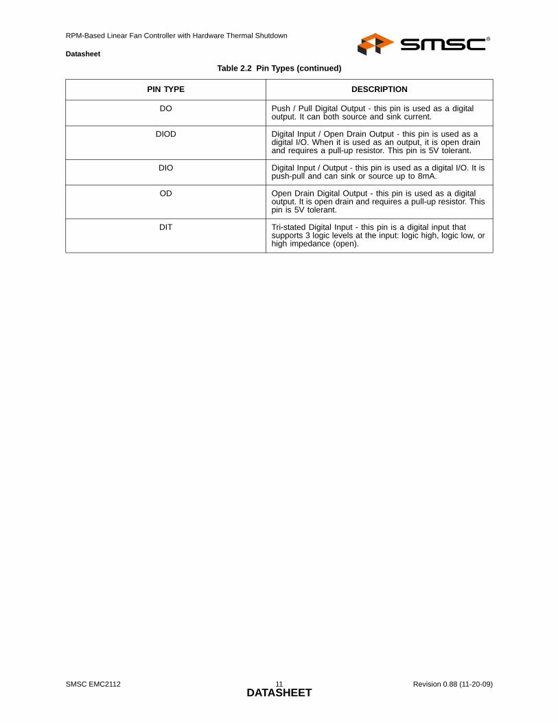
Table 2.2 Pin Types
PIN TYPE DESCRIPTION
Power This pin is used to supply power or ground to the device.
DI Digital Input - this pin is used as a digital input. This pin is 5V tolerant.
AO Analog Output - this pin is used as an output for analog signals.
AIO Analog Input / Output - this pin is used as an I/O for analog signals.
Table 2.1 Pin Description (continued)
PIN NAME FUNCTION TYPE
Revision 0.88 (11-20-09) 10 SMSC EMC2112DATASHEET
RPM-Based Linear Fan Controller with Hardware Thermal Shutdown
Datasheet
DO Push / Pull Digital Output - this pin is used as a digital output. It can both source and sink current.
DIOD Digital Input / Open Drain Output - this pin is used as a digital I/O. When it is used as an output, it is open drain and requires a pull-up resistor. This pin is 5V tolerant.
DIO Digital Input / Output - this pin is used as a digital I/O. It is push-pull and can sink or source up to 8mA.
OD Open Drain Digital Output - this pin is used as a digital output. It is open drain and requires a pull-up resistor. This pin is 5V tolerant.
DIT Tri-stated Digital Input - this pin is a digital input that supports 3 logic levels at the input: logic high, logic low, or high impedance (open).
Table 2.2 Pin Types (continued)
PIN TYPE DESCRIPTION
SMSC EMC2112 11 Revision 0.88 (11-20-09)DATASHEET
RPM-Based Linear Fan Controller with Hardware Thermal Shutdown
Datasheet
Chapter 3 Electrical Specifications
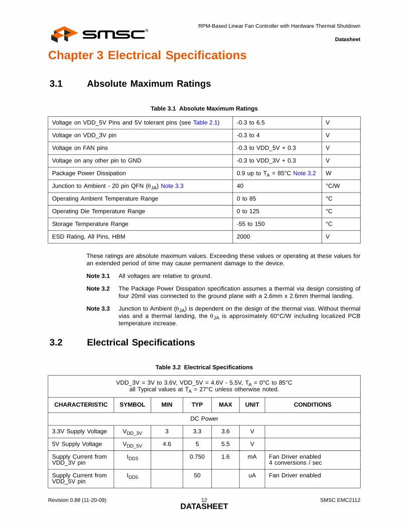
3.1 Absolute Maximum Ratings
These ratings are absolute maximum values. Exceeding these values or operating at these values foran extended period of time may cause permanent damage to the device.
Note 3.1 All voltages are relative to ground.
Note 3.2 The Package Power Dissipation specification assumes a thermal via design consisting offour 20mil vias connected to the ground plane with a 2.6mm x 2.6mm thermal landing.
Note 3.3 Junction to Ambient (θJA) is dependent on the design of the thermal vias. Without thermalvias and a thermal landing, the θJA is approximately 60°C/W including localized PCBtemperature increase.
3.2 Electrical Specifications
Table 3.1 Absolute Maximum Ratings
Voltage on VDD_5V Pins and 5V tolerant pins (see Table 2.1) -0.3 to 6.5 V
Voltage on VDD_3V pin -0.3 to 4 V
Voltage on FAN pins -0.3 to VDD_5V + 0.3 V
Voltage on any other pin to GND -0.3 to VDD_3V + 0.3 V
Package Power Dissipation 0.9 up to TA = 85°C Note 3.2 W
Junction to Ambient - 20 pin QFN (θJA) Note 3.3 40 °C/W
Operating Ambient Temperature Range 0 to 85 °C
Operating Die Temperature Range 0 to 125 °C
Storage Temperature Range -55 to 150 °C
ESD Rating, All Pins, HBM 2000 V
Table 3.2 Electrical Specifications
VDD_3V = 3V to 3.6V, VDD_5V = 4.6V - 5.5V, TA = 0°C to 85°Call Typical values at TA = 27°C unless otherwise noted.
CHARACTERISTIC SYMBOL MIN TYP MAX UNIT CONDITIONS
DC Power
3.3V Supply Voltage VDD_3V 3 3.3 3.6 V
5V Supply Voltage VDD_5V 4.6 5 5.5 V
Supply Current from VDD_3V pin
IDD3 0.750 1.6 mA Fan Driver enabled4 conversions / sec
Supply Current from VDD_5V pin
IDD5 50 uA Fan Driver enabled
Revision 0.88 (11-20-09) 12 SMSC EMC2112DATASHEET
RPM-Based Linear Fan Controller with Hardware Thermal Shutdown
Datasheet
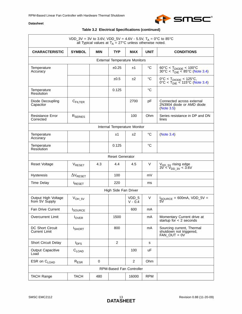
External Temperature Monitors
Temperature Accuracy
±0.25 ±1 °C 60°C < TDIODE < 100°C30°C < TDIE < 85°C (Note 3.4)
±0.5 ±2 °C 0°C < TDIODE < 125°C, 0°C < TDIE < 115°C (Note 3.4)
Temperature Resolution
0.125 °C
Diode Decoupling Capacitor
CFILTER 2700 pF Connected across external 2N3904 diode or AMD diode (Note 3.5)
Resistance Error Corrected
RSERIES 100 Ohm Series resistance in DP and DN lines
Internal Temperature Monitor
Temperature Accuracy
±1 ±2 °C (Note 3.4)
Temperature Resolution
0.125 °C
Reset Generator
Reset Voltage VRESET 4.3 4.4 4.5 V VDD_5V rising edge3V < VDD_3V < 3.6V
Hysteresis ΔVRESET 100 mV
Time Delay tRESET 220 ms
High Side Fan Driver
Output High Voltage from 5V Supply
VOH_5V VDD_5V - 0.4
V ISOURCE = 600mA, VDD_5V = 5V
Fan Drive Current ISOURCE 600 mA
Overcurrent Limit IOVER 1500 mA Momentary Current drive at startup for < 2 seconds
DC Short Circuit Current Limit
ISHORT 800 mA Sourcing current, Thermal shutdown not triggered, FAN_OUT = 0V
Short Circuit Delay tDFS 2 s
Output Capacitive Load
CLOAD 100 uF
ESR on CLOAD RESR 0 2 Ohm
RPM-Based Fan Controller
TACH Range TACH 480 16000 RPM
Table 3.2 Electrical Specifications (continued)
VDD_3V = 3V to 3.6V, VDD_5V = 4.6V - 5.5V, TA = 0°C to 85°Call Typical values at TA = 27°C unless otherwise noted.
CHARACTERISTIC SYMBOL MIN TYP MAX UNIT CONDITIONS
SMSC EMC2112 13 Revision 0.88 (11-20-09)DATASHEET
RPM-Based Linear Fan Controller with Hardware Thermal Shutdown
Datasheet
Note 3.4 TDIE refers to the internal die temperature and may not match TA due to self heating ofthe device. The internal temperature sensor will return TDIE.
Note 3.5 Contact SMSC for Application Notes and guidelines when measuring GPU processordiodes and CPU processor diodes.
Note 3.6 The ALERT, SYS_SHDN, SMDATA, and SMCLK pins will not glitch low upon power upwhen pulled to VDD or another voltage.
3.3 SMBus Electrical Specifications
RPM Control Accuracy
ΔTACH ±0.25 ±0.5 % External oscillator 32.768kHz
ΔTACH ±0.5 ±1 % Internal Oscillator 40°C < TDIE < 100°C
Thermal Shutdown
Thermal Shutdown Threshold
TSDTH 150 °C
Thermal Shutdown Hysteresis
TSDHYST 50 °C
SMBus and Digital I/O pins
Output High Voltage VOH VDD _3V-0.4
V 4 mA current drive
Output Low Voltage VOL 0.5 V 4 mA current sink
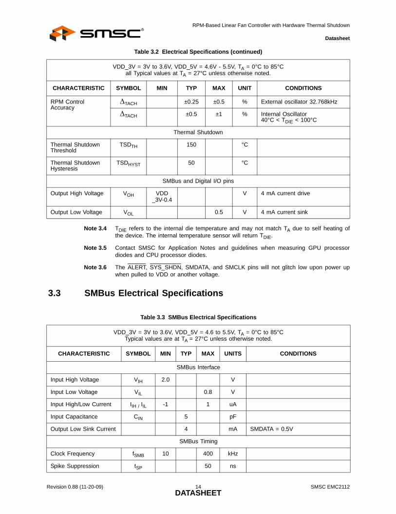
Table 3.3 SMBus Electrical Specifications
VDD_3V = 3V to 3.6V, VDD_5V = 4.6 to 5.5V, TA = 0°C to 85°CTypical values are at TA = 27°C unless otherwise noted.
CHARACTERISTIC SYMBOL MIN TYP MAX UNITS CONDITIONS
SMBus Interface
Input High Voltage VIH 2.0 V
Input Low Voltage VIL 0.8 V
Input High/Low Current IIH / IIL -1 1 uA
Input Capacitance CIN 5 pF
Output Low Sink Current 4 mA SMDATA = 0.5V
SMBus Timing
Clock Frequency fSMB 10 400 kHz
Spike Suppression tSP 50 ns
Table 3.2 Electrical Specifications (continued)
VDD_3V = 3V to 3.6V, VDD_5V = 4.6V - 5.5V, TA = 0°C to 85°Call Typical values at TA = 27°C unless otherwise noted.
CHARACTERISTIC SYMBOL MIN TYP MAX UNIT CONDITIONS
Revision 0.88 (11-20-09) 14 SMSC EMC2112DATASHEET

RPM-Based Linear Fan Controller with Hardware Thermal Shutdown
Datasheet
Bus Free Time Start to Stop
tBUF 1.3 us
Setup Time: Start tSU:STA 0.6 us
Setup Time: Stop tSU:STP 0.6 us
Data Hold Time tHD:DAT 0.6 6 us
Data Setup Time tSU:DAT 0.6 72 us
Clock Low Period tLOW 1.3 us
Clock High Period tHIGH 0.6 us
Clock/Data Fall time tFALL 300 ns Min = 20+0.1CLOAD ns
Clock/Data Rise time tRISE 300 ns Min = 20+0.1CLOAD ns
Capacitive Load CLOAD 400 pF per bus line
Table 3.3 SMBus Electrical Specifications (continued)
VDD_3V = 3V to 3.6V, VDD_5V = 4.6 to 5.5V, TA = 0°C to 85°CTypical values are at TA = 27°C unless otherwise noted.
CHARACTERISTIC SYMBOL MIN TYP MAX UNITS CONDITIONS
SMSC EMC2112 15 Revision 0.88 (11-20-09)DATASHEET

RPM-Based Linear Fan Controller with Hardware Thermal Shutdown
Datasheet
Chapter 4 System Management Bus Interface Protocol
4.1 System Management Bus Interface ProtocolThe EMC2112 communicates with a host controller, such as an SMSC SIO, through the SMBus. TheSMBus is a two-wire serial communication protocol between a computer host and its peripheraldevices. A detailed timing diagram is shown in Figure 4.1. Stretching of the SMCLK signal is supported,however the EMC2112 will not stretch the clock signal.
4.1.1 SMBus Start Bit
The SMBus Start bit is defined as a transition of the SMBus Data line from a logic ‘1’ state to a logic‘0’ state while the SMBus Clock line is in a logic ‘1’ state. When the EMC2112 detects an SMBus Startbit, it will disable the BC-Link protocol circuitry and communicate using the SMBus Protocol
4.1.2 SMBus Address and RD / WR Bit
The SMBus Address Byte consists of the 7-bit client address followed by a -bit RD / WR indicator. Ifthis RD / WR bit is a logic ‘0’, then the SMBus Host is writing data to the client device. If this RD / WRbit is a logic ‘1’, then the SMBus Host is reading data from the client device.
The slave address is determined at power up by the pin-state of the ADDR_SEL pin as shown inTable 4.1.
Figure 4.1 SMBus Timing Diagram
Table 4.1 ADDR_SEL Pin Configuration
ADDR_SEL PIN STATE SMBUS SLAVE ADDRESS
‘0’ 0101_111xb
‘High Z’ 0111_101xb
‘1’ 0101_110xb
SMDATA
SMCLK
TBUF
P S S - Start Condition P - Stop Condition PS
T HIGHT LOW T HD:STA T SU:STO
T HD:STAT HD:DAT
T SU:DAT T SU:STA
T FALL
T RISE
Revision 0.88 (11-20-09) 16 SMSC EMC2112DATASHEET
RPM-Based Linear Fan Controller with Hardware Thermal Shutdown
Datasheet
4.1.3 SMBus Data Bytes
All SMBus Data bytes are sent most significant bit first and composed of 8-bits of information.
4.1.4 SMBus ACK and NACK Bits
The SMBus client will acknowledge all data bytes that it receives (as well as the client address if itmatches and the ARA address if the ATF_INT# pin is asserted). This is done by the client devicepulling the SMBus Data line low after the 8th bit of each byte that is transmitted.
The Host will NACK (not acknowledge) the data received from the client by holding the SMBus dataline high after the 8th data bit has been sent.
4.1.5 SMBus Stop Bit
The SMBus Stop bit is defined as a transition of the SMBus Data line from a logic ‘0’ state to a logic‘1’ state while the SMBus clock line is in a logic ‘1’ state. When the EMC2112 detects an SMBus Stopbit, and it has been communicating with the SMBus protocol, it will reset its client interface and prepareto receive further communications.
4.1.6 SMBus Time-out
The EMC2112 includes an SMBus time-out feature. Following a 30ms period of inactivity on theSMBus, the device will time-out and reset the SMBus interface. The timeout can be disabled by settingthe DIS_TO bit in the Configuration 2 register.
4.1.7 SMBus and I2C Compliance
The major difference between SMBus and I2C devices is highlighted here. For complete complianceinformation refer to the SMBus 2.0 specification.
1. Minimum frequency for SMBus communications is 10kHz.
2. The client protocol will reset if the clock is held for longer than 30ms.
3. The slave protocol will reset if both the clock and data lines are held high for longer than 150us.
4. I2C devices do not support the Alert Response Address functionality (which is optional for SMBus).
5. The Block Read and Block Write protocols are only compliant with I2C data formatting. They donot support SMBus formatting for Block Read and Block Write protocols.
4.2 SMBus Protocols The EMC2112 is SMBus 2.0 compatible and supports Send Byte, Read Byte, Receive Byte and WriteByte as valid protocols as shown below. It will respond to the Alert Response Address protocol but isnot in full compliance.
All of the below protocols use the convention in Table 4.2.
Table 4.2 Protocol Format
DATA SENT TO DEVICE
DATA SENT TO THE HOST
# of bits sent # of bits sent
SMSC EMC2112 17 Revision 0.88 (11-20-09)DATASHEET

RPM-Based Linear Fan Controller with Hardware Thermal Shutdown
Datasheet
4.2.1 Write Byte
The Write Byte is used to write one byte of data to the registers as shown below Table 4.3:
4.2.2 Read Byte
The Read Byte protocol is used to read one byte of data from the registers as shown in Table 4.4.
4.2.3 Send Byte
The Send Byte protocol is used to set the internal address register pointer to the correct addresslocation. No data is transferred during the Send Byte protocol as shown in Table 4.5.
4.2.4 Receive Byte
The Receive Byte protocol is used to read data from a register when the internal register addresspointer is known to be at the right location (e.g. set via Send Byte). This is used for consecutive readsof the same register as shown in Table 4.6.
Table 4.3 Write Byte Protocol
STARTSLAVE
ADDRESS WR ACKREGISTER ADDRESS ACK
REGISTER DATA ACK STOP
1 -> 0 0111_101 0 0 XXh 0 XXh 0 0 -> 1
Table 4.4 Read Byte Protocol
START SLAVE ADDRESS
WR ACK Register Address
ACK START Slave Address
RD ACK Register Data
NACK STOP
1 -> 0 0111_101 0 0 XXh 0 0 -> 1 0111_101 1 0 XXh 1 0 -> 1
Table 4.5 Send Byte Protocol
STARTSLAVE
ADDRESS WR ACKREGISTER ADDRESS ACK STOP
1 -> 0 0111_101 0 0 XXh 0 0 -> 1
Table 4.6 Receive Byte Protocol
STARTSLAVE
ADDRESS RD ACK REGISTER DATA NACK STOP
1 -> 0 0111_101 1 0 XXh 1 0 -> 1
Revision 0.88 (11-20-09) 18 SMSC EMC2112DATASHEET
RPM-Based Linear Fan Controller with Hardware Thermal Shutdown
Datasheet
START EGISTER DATA
1->0 XXh
ACK STOP
0 0 -> 1
4.2.5 Block Write Protocol
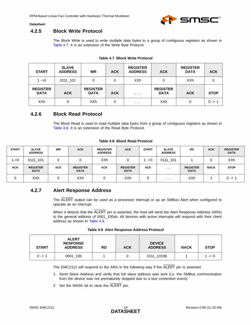
The Block Write is used to write multiple data bytes to a group of contiguous registers as shown inTable 4.7. It is an extension of the Write Byte Protocol.
4.2.6 Block Read Protocol
The Block Read is used to read multiple data bytes from a group of contiguous registers as shown inTable 4.8. It is an extension of the Read Byte Protocol.
4.2.7 Alert Response Address
The ALERT output can be used as a processor interrupt or as an SMBus Alert when configured tooperate as an interrupt.
When it detects that the ALERT pin is asserted, the host will send the Alert Response Address (ARA)to the general address of 0001_100xb. All devices with active interrupts will respond with their clientaddress as shown in Table 4.9.
The EMC2112 will respond to the ARA in the following way if the ALERT pin is asserted.
1. Send Slave Address and verify that full slave address was sent (i.e. the SMBus communicationfrom the device was not prematurely stopped due to a bus contention event).
2. Set the MASK bit to clear the ALERT pin.
Table 4.7 Block Write Protocol
STARTSLAVE
ADDRESS WR ACKREGISTER ADDRESS ACK
REGISTER DATA ACK
1 ->0 0111_101 0 0 XXh 0 XXh 0
REGISTER DATA ACK
REGISTER DATA ACK . . .
REGISTER DATA ACK STOP
XXh 0 XXh 0 . . . XXh 0 0 -> 1
Table 4.8 Block Read Protocol
SLAVE ADDRESS
WR ACK REGISTER ADDRESS
ACK START SLAVE ADDRESS
RD ACK R
0111_101 0 0 XXh 0 1 ->0 0111_101 1 0
REGISTER DATA
ACK REGISTER DATA
ACK REGISTER DATA
ACK . . . REGISTER DATA
NACK
XXh 0 XXh 0 XXh 0 . . . XXh 1
Table 4.9 Alert Response Address Protocol
START
ALERT RESPONSE ADDRESS RD ACK
DEVICE ADDRESS NACK STOP
0 -> 1 0001_100 1 0 0111_1010b 1 1 -> 0
SMSC EMC2112 19 Revision 0.88 (11-20-09)DATASHEET
RPM-Based Linear Fan Controller with Hardware Thermal Shutdown
Datasheet
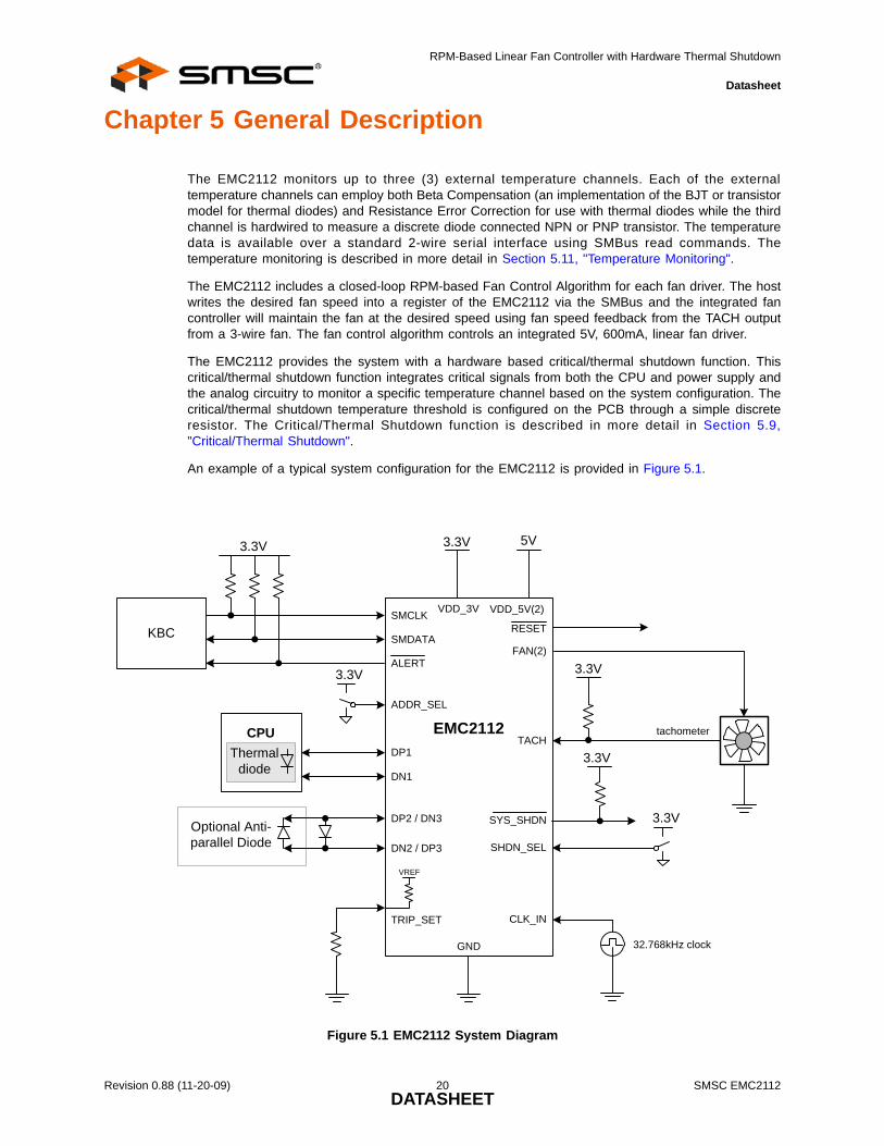
Chapter 5 General Description
The EMC2112 monitors up to three (3) external temperature channels. Each of the externaltemperature channels can employ both Beta Compensation (an implementation of the BJT or transistormodel for thermal diodes) and Resistance Error Correction for use with thermal diodes while the thirdchannel is hardwired to measure a discrete diode connected NPN or PNP transistor. The temperaturedata is available over a standard 2-wire serial interface using SMBus read commands. Thetemperature monitoring is described in more detail in Section 5.11, "Temperature Monitoring".
The EMC2112 includes a closed-loop RPM-based Fan Control Algorithm for each fan driver. The hostwrites the desired fan speed into a register of the EMC2112 via the SMBus and the integrated fancontroller will maintain the fan at the desired speed using fan speed feedback from the TACH outputfrom a 3-wire fan. The fan control algorithm controls an integrated 5V, 600mA, linear fan driver.
The EMC2112 provides the system with a hardware based critical/thermal shutdown function. Thiscritical/thermal shutdown function integrates critical signals from both the CPU and power supply andthe analog circuitry to monitor a specific temperature channel based on the system configuration. Thecritical/thermal shutdown temperature threshold is configured on the PCB through a simple discreteresistor. The Critical/Thermal Shutdown function is described in more detail in Section 5.9,"Critical/Thermal Shutdown".
An example of a typical system configuration for the EMC2112 is provided in Figure 5.1.
Figure 5.1 EMC2112 System Diagram
EMC2112DP1
DN1
DP2 / DN3
DN2 / DP3
CPUThermal
diode
3.3V
SMCLK
SMDATA
ALERT
VDD_3V
TACH
3.3V
KBC
ADDR_SEL
GND
tachometer
RESET
3.3V
5V
VDD_5V(2)
FAN(2)
3.3V
SYS_SHDN
SHDN_SEL
CLK_IN
32.768kHz clock
VREF
TRIP_SET
3.3V
3.3V
Optional Anti-parallel Diode
Revision 0.88 (11-20-09) 20 SMSC EMC2112DATASHEET
RPM-Based Linear Fan Controller with Hardware Thermal Shutdown
Datasheet
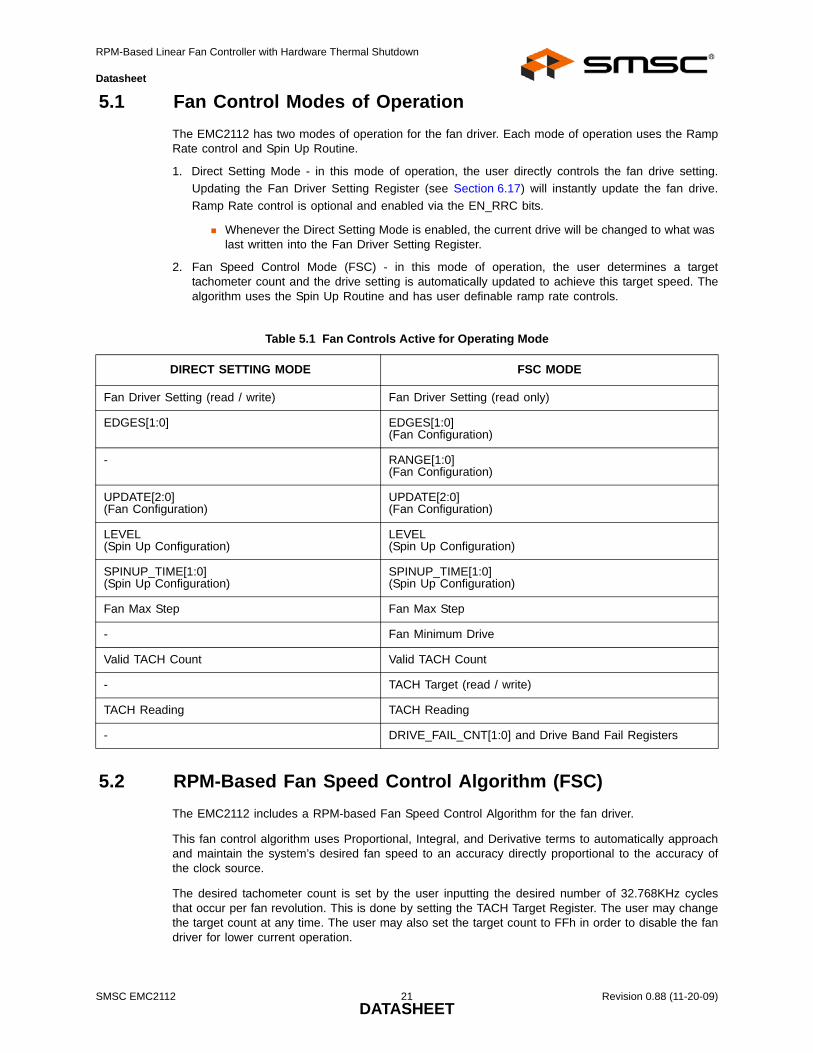
5.1 Fan Control Modes of OperationThe EMC2112 has two modes of operation for the fan driver. Each mode of operation uses the RampRate control and Spin Up Routine.
1. Direct Setting Mode - in this mode of operation, the user directly controls the fan drive setting.Updating the Fan Driver Setting Register (see Section 6.17) will instantly update the fan drive.Ramp Rate control is optional and enabled via the EN_RRC bits.
Whenever the Direct Setting Mode is enabled, the current drive will be changed to what was last written into the Fan Driver Setting Register.
2. Fan Speed Control Mode (FSC) - in this mode of operation, the user determines a targettachometer count and the drive setting is automatically updated to achieve this target speed. Thealgorithm uses the Spin Up Routine and has user definable ramp rate controls.
5.2 RPM-Based Fan Speed Control Algorithm (FSC)The EMC2112 includes a RPM-based Fan Speed Control Algorithm for the fan driver.
This fan control algorithm uses Proportional, Integral, and Derivative terms to automatically approachand maintain the system’s desired fan speed to an accuracy directly proportional to the accuracy ofthe clock source.
The desired tachometer count is set by the user inputting the desired number of 32.768KHz cyclesthat occur per fan revolution. This is done by setting the TACH Target Register. The user may changethe target count at any time. The user may also set the target count to FFh in order to disable the fandriver for lower current operation.
Table 5.1 Fan Controls Active for Operating Mode
DIRECT SETTING MODE FSC MODE
Fan Driver Setting (read / write) Fan Driver Setting (read only)
EDGES[1:0] EDGES[1:0] (Fan Configuration)
- RANGE[1:0](Fan Configuration)
UPDATE[2:0] (Fan Configuration)
UPDATE[2:0] (Fan Configuration)
LEVEL(Spin Up Configuration)
LEVEL(Spin Up Configuration)
SPINUP_TIME[1:0] (Spin Up Configuration)
SPINUP_TIME[1:0] (Spin Up Configuration)
Fan Max Step Fan Max Step
- Fan Minimum Drive
Valid TACH Count Valid TACH Count
- TACH Target (read / write)
TACH Reading TACH Reading
- DRIVE_FAIL_CNT[1:0] and Drive Band Fail Registers
SMSC EMC2112 21 Revision 0.88 (11-20-09)DATASHEET
RPM-Based Linear Fan Controller with Hardware Thermal Shutdown
Datasheet
For example, if a desired RPM rate for a 2-pole fan is 3000 RPMs, then the user would input thehexidecimal equivalent of 1296 (51h in the TACH Target Register). This number represents the numberof 32.768KHz cycles that would occur during the time it takes the fan to complete a single revolutionwhen it is spinning at 3000RPMs.
The EMC2112’s RPM-based Fan Speed Control Algorithm has programmable configuration settingsfor parameters such as ramp-rate control and spin up conditions. The fan driver automatically detectsand attempts to alleviate a stalled/stuck fan condition while also asserting the ALERT pin. TheEMC2112 works with fans that operate up to 16,000 RPMs and provide a valid tachometer signal. Thefan controller will function either with an externally supplied 32.768KHz clock source or with it’s owninternal 32kHz oscillator depending on the required accuracy.
5.2.1 Programming the RPM-Based Fan Speed Control Algorithm
The RPM-based Fan Speed Control Algorithm is disabled upon device power up. The followingregisters control the algorithm. The EMC2112 fan control registers are pre-loaded with defaults thatwill work for a wide variety of fans so only the TACH Target Register is required to set a fan speed.The other fan control registers can be used to fine-tune the algorithm behavior based on applicationrequirements.
Note that steps 1 - 6 are optional and need only be performed if the default settings do not providethe desired fan response.
1. Set the Spin Up Configuration Register to the Spin Up Level and Spin Time desired.
2. Set the Fan Step Register to the desired step size.
3. Set the Fan Minimum Drive Register to the minimum drive value that will maintain fan operation.
4. Set the Update Time, and Edges options in the Fan Configuration Register.
5. Set the Valid TACH Count Register to the highest tach count that indicates the fan is spinning.
6. Set the TACH Target Register to the desired tachometer count.
7. Enable the RPM-based Fan Speed Control Algorithm by setting the EN_ALGO bit.
5.3 Tachometer MeasurementThe tachometer measurement circuitry is used in conjunction with the RPM-based Fan Speed ControlAlgorithm to update the fan driver output. Additionally, it can be used in Direct Setting mode as adiagnostic for host based fan control.
This method monitors the TACH signal in real time. It constantly updates the tachometer measurementby reporting the number of clocks between a user programmed number of edges on the TACH signal.
The tachometer measurement provides fast response times for the RPM-based Fan Speed ControlAlgorithm and the data is presented as a count value that represents the fan RPM period. When thismethod is used, all fan target values must be input as a count value for proper operation.
APPLICATION NOTE: The tachometer measurement method works independently of the drive settings. If thedevice is put into Direct Setting and the fan drive is set at a level that is lower than the fancan operate (including zero drive), then the tachometer measurement may signal a StalledFan condition and assert an interrupt.
5.3.1 Stalled Fan
A Stalled fan is detected if the tach counter exceeds the user-programmable Valid TACH Count settingthen it will flag the fan as stalled and trigger an interrupt.
If the RPM-based Fan Speed Control Algorithm is enabled, the algorithm will automatically attempt torestart the fan until it detects a valid tachometer level or is disabled.
Revision 0.88 (11-20-09) 22 SMSC EMC2112DATASHEET
RPM-Based Linear Fan Controller with Hardware Thermal Shutdown
Datasheet
The FAN_STALL Status bit indicates that a stalled fan was detected. This bit is checked conditionallydepending on the mode of operation.
Whenever the Direct Setting Mode is enabled or whenever the Spin Up Routine is enabled, the FAN_STALL interrupt will be masked for the duration of the programmed Spin Up Time (see Section 6.21) to allow the fan an opportunity to reach a valid speed without generating unnecessary interrupts.
In Direct Setting Mode with the tachometer measurement using the Tach Period Measurement method, whenever the TACH Reading Register value exceeds the Valid TACH Count Register setting, the FAN_STALL status bit will be set.
When using the RPM-based Fan Speed Control Algorithm, the stalled fan condition is checked whenever the Update Time is met and the fan drive setting is updated. It is not a continuous check.
5.3.2 Aging Fan or Invalid Drive Detection
This is useful to detect aging fan conditions (where the fan’s natural maximum speed degrades overtime) or incorrect fan speed settings. The EMC2112 contains circuitry that detects that the programmedfan speed can be reached by the fan. If the target fan speed cannot be reached within a user definedband of tach counts at maximum drive then the DRIVE_FAIL status bits are set and the ALERT pin isasserted.
5.3.3 Clock Source
The CLK pin can be configured as an input for the EMC2112 or as an output to drive additional deviceswith the internally generated tachometer clock (see Section 6.9).
When the CLK pin is configured as an input to the EMC2112, then a 32.768kHz clock must beprovided. This clock is used to by the Tachometer measurement circuitry and will directly affect theaccuracy of this measurement.
When the CLK pin is configured as an output, then it will be driven at the same frequency as theinternal tachometer clock.
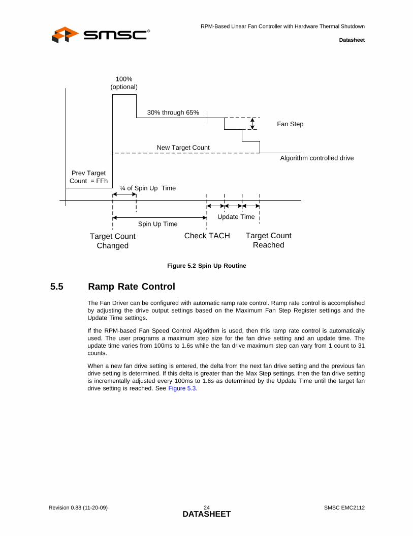
5.4 Spin Up RoutineThe EMC2112 also contains programmable circuitry to control the spin up behavior of the fan driverto ensure proper fan operation.
The Spin Up Routine is initiated in Direct Setting mode when the setting value changes from 00h toanything else.
When the Fan Speed Control Algorithm is enabled, the Spin Up Routine is initiated under the followingconditions when the Tach Period Measurement method of tach measurement is used:
1. The TACH Target Register value changes from a value of FFh to a value that is less than the ValidTACH Count (see Section 6.24).
2. The RPM-based Fan Speed Control Algorithm’s measured TACH Reading Register value is greaterthan the Valid TACH Count setting.
When the Spin Up Routine is operating, the fan driver is set to full scale (optional) for one quarter ofthe total user defined spin up time. For the remaining spin up time, the fan driver output is set a a userdefined level (30% through 65% drive).
After the Spin Up Routine has finished, the EMC2112 measures the TACH signal. If the measuredTACH Reading Register value is higher than the Valid TACH Count Register setting, the FAN_SPINstatus bit is set and the Spin Up Routine will automatically attempt to restart the fan.
Figure 5.2 shows an example of the Spin Up Routine in response to a programmed fan speed changebased on the first condition above.
SMSC EMC2112 23 Revision 0.88 (11-20-09)DATASHEET
RPM-Based Linear Fan Controller with Hardware Thermal Shutdown
Datasheet
5.5 Ramp Rate ControlThe Fan Driver can be configured with automatic ramp rate control. Ramp rate control is accomplishedby adjusting the drive output settings based on the Maximum Fan Step Register settings and theUpdate Time settings.
If the RPM-based Fan Speed Control Algorithm is used, then this ramp rate control is automaticallyused. The user programs a maximum step size for the fan drive setting and an update time. Theupdate time varies from 100ms to 1.6s while the fan drive maximum step can vary from 1 count to 31counts.
When a new fan drive setting is entered, the delta from the next fan drive setting and the previous fandrive setting is determined. If this delta is greater than the Max Step settings, then the fan drive settingis incrementally adjusted every 100ms to 1.6s as determined by the Update Time until the target fandrive setting is reached. See Figure 5.3.
Figure 5.2 Spin Up Routine
100%(optional)
30% through 65%
Algorithm controlled drive
Fan Step
Spin Up Time
¼ of Spin Up Time
Update Time
Target Count Changed
Target Count Reached
New Target Count
Prev Target Count = FFh
Check TACH
Revision 0.88 (11-20-09) 24 SMSC EMC2112DATASHEET

RPM-Based Linear Fan Controller with Hardware Thermal Shutdown
Datasheet
5.5.1 Temperature Bypass of Ramp Rate Control
As an optional feature, the Ramp Rate Control functionality can be disabled if any of the measuredtemperature channels exceed their respective high limits. In this mode, once the high limit has beenexceeded, the ramp rate controls are removed which allows the fan to move instantly to theprogrammed drive setting (using the FSC or in manual mode).
5.6 Watchdog TimerThe EMC2112 contains an internal Watchdog Timer for the fan driver. The Watchdog timer monitorsthe SMBus traffic for signs of activity and works in two different modes based upon device operation.These modes are Power Up Operation and Continuous Operation as described below.
For either mode of operation, if four (4) seconds elapse without activity detected by the host, then thewatchdog will be triggered and the following will occur:
1. The WATCH status bit will be set which will cause the ALERT pin to be asserted.
2. The fan driver will be set to full scale drive. It will remain at full scale drive until it is disabled.
APPLICATION NOTE: When the Watchdog timer is activated the Fan Speed Control Algorithm is automaticallydisabled. Disabling the Watchdog will not automatically set the fan drive nor re-activate theFan Speed Control Algorithm. This must be done manually.
Figure 5.3 Ramp Rate Control
Previous Setting
Next Desired Setting
Max Step
Max Step
Update Time
Update Time
Setting Changed
SMSC EMC2112 25 Revision 0.88 (11-20-09)DATASHEET

RPM-Based Linear Fan Controller with Hardware Thermal Shutdown
Datasheet
5.6.1 Power Up Operation
The Watchdog Timer only starts immediately after power-up and once it has been triggered ordeactivated will not restart (however can be configured to operate in Continuous operation)
In the Power Up Operation, the Watchdog Timer is disabled by any of the following actions:
1. Writing the Fan Setting Register will disable the Watchdog Timer.
2. Enabling the RPM-based Fan Speed Control Algorithm by setting the EN_ALGO bit will disable theWatchdog Timer. The fan driver will be set based on the RPM-based Fan Speed Control Algorithm.
3. Changing the Watchdog operating mode by setting the WD_EN bit.
Writing any other configuration registers will not disable the Watchdog Timer upon power up.
5.6.2 Continuous Operation
When configured to operate in Continuous Operation, the Watchdog timer will start immediately. It canbe disabled by any access (read or write) to the SMBus register set. Upon completion of SMBusactivity, the Watchdog timer is reset and restarted.
5.7 High Side Fan DriverThe EMC2112’s integrates a 5V, 600mA, linear high side fan driver to directly drive a 5V fan. By fullyintegrating the linear fan driver, the typical requirement for the discrete pass device and other externallinearization circuitry is completely eliminated.
5.7.1 Overcurrent Limit
The High Side Fan Driver contains circuitry to allow for significant over current levels to accommodatetransient conditions on the FAN pins. The over current limit is dependent upon the output voltage withthe limit dropping as the voltage nears 0V.
If the fan driver current detects a short-circuit condition for longer than 2 seconds, then the I_SHORTstatus bit is set and an interrupt generated. Additionally, the High Side Fan Driver will be disabled for8 seconds. After this 8 second time has elapsed, it will be allowed to restart invoking the Spin UpRoutine before returning to its previous drive setting.
APPLICATION NOTE: If the FSC Algorithm is active, then it will generate errant SPIN_FAIL interrupts during the 8second time that the fan driver is held off.
5.8 Internal Thermal Shutdown (TSD)The EMC2112 contains an internal thermal shutdown circuit that monitors the internal die temperature.If the die temperature exceeds the Thermal Shutdown Threshold (see Table 3.2), then the followingwill occur:
1. The High Side Fan Driver is disabled. It will remain disabled until the internal temperature dropsbelow the threshold temperature minus 50°C.
2. The TSD Status bit is set.
3. The SYS_SHDN pin is asserted.
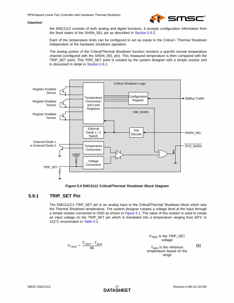
5.9 Critical/Thermal ShutdownThe EMC2112 provides a hardware Critical/Thermal Shutdown function for systems. Figure 5.4 is ablock diagram of this Critical/Thermal Shutdown function. The Critical/Thermal Shutdown function in
Revision 0.88 (11-20-09) 26 SMSC EMC2112DATASHEET
RPM-Based Linear Fan Controller with Hardware Thermal Shutdown
Datasheet
the EMC2112 consists of both analog and digital functions. It accepts configuration information fromthe fixed states of the SHDN_SEL pin as described in Section 5.9.2.
Each of the temperature limits can be configured to act as inputs to the Critical / Thermal Shutdownindependent of the hardware shutdown operation.
The analog portion of the Critical/Thermal Shutdown function monitors a specific remote temperaturechannel (configured with the SHDN_SEL pin). This measured temperature is then compared with theTRIP_SET point. This TRIP_SET point is created by the system designer with a simple resistor andis discussed in detail in Section 5.9.1.
5.9.1 TRIP_SET Pin
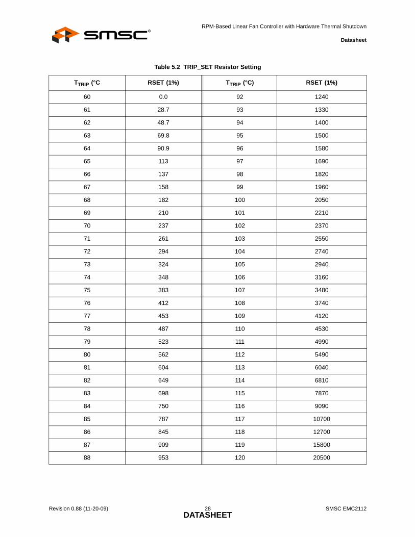
The EMC2112’s TRIP_SET pin is an analog input to the Critical/Thermal Shutdown block which setsthe Thermal Shutdown temperature. The system designer creates a voltage level at the input througha simple resistor connected to GND as shown in Figure 5.1. The value of this resistor is used to createan input voltage on the TRIP_SET pin which is translated into a temperature ranging from 60°C to122°C enumerated in Table 5.2.
Figure 5.4 EMC2112 Critical/Thermal Shutdown Block Diagram
VTRIP is the TRIP_SET voltage
[1]TMIN is the minimum temperature based on the
range
SYS_SHDN
TRIP_SET
External Diode 1 or External Diode 2
Critical Shutdown Logic
SMBus Traffic
SW_SHDN
Configuration Register
VREF
SHDN_SELPIN
Decode
Register Enabled Sensor
External Diode 1 / 2
Switch
Voltage Conversion
Temperature Conversion
Temperature Conversion and Limit Registers
Register Enabled Sensor
Register Enabled Sensor
VTRIPTTRIP TMIN–
80----------------------------------=
SMSC EMC2112 27 Revision 0.88 (11-20-09)DATASHEET
RPM-Based Linear Fan Controller with Hardware Thermal Shutdown
Datasheet
Table 5.2 TRIP_SET Resistor Setting
TTRIP (°C RSET (1%) TTRIP (°C) RSET (1%)
60 0.0 92 1240
61 28.7 93 1330
62 48.7 94 1400
63 69.8 95 1500
64 90.9 96 1580
65 113 97 1690
66 137 98 1820
67 158 99 1960
68 182 100 2050
69 210 101 2210
70 237 102 2370
71 261 103 2550
72 294 104 2740
73 324 105 2940
74 348 106 3160
75 383 107 3480
76 412 108 3740
77 453 109 4120
78 487 110 4530
79 523 111 4990
80 562 112 5490
81 604 113 6040
82 649 114 6810
83 698 115 7870
84 750 116 9090
85 787 117 10700
86 845 118 12700
87 909 119 15800
88 953 120 20500
Revision 0.88 (11-20-09) 28 SMSC EMC2112DATASHEET
RPM-Based Linear Fan Controller with Hardware Thermal Shutdown
Datasheet
5.9.2 SHDN_SEL Pin
The EMC2112 has one ‘strappable’ input (SHDN_SEL) allowing for configuration of the hardwareCritical/Thermal Shutdown. This pin has 3 possible states and is monitored and decoded by theEMC2112 at power-up. The three possible states are 0 (tied to GND), 1 (tied to 3.3V) or High-Z (open).The states of this pin determine which remote temperature channel and configuration is used by theCritical/Thermal Shutdown function. The different configurations of SHDN_SEL pin are described inTable 5.3
A channel that is configured via the SHDN_SEL pin for the Critical/Thermal Shutdown is locked andnone of the configuration registers associated with it can be updated via the SMBus. The other twotemperature channels, however, are still configurable via the SMBus.
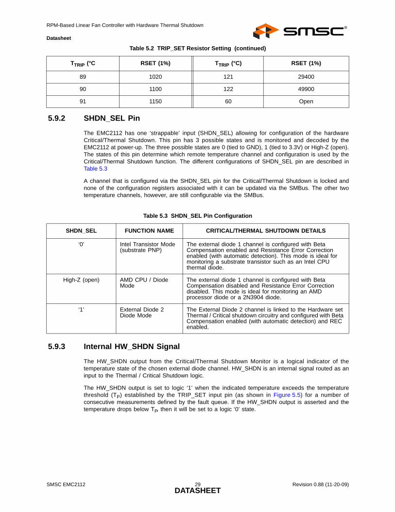
5.9.3 Internal HW_SHDN Signal
The HW_SHDN output from the Critical/Thermal Shutdown Monitor is a logical indicator of thetemperature state of the chosen external diode channel. HW_SHDN is an internal signal routed as aninput to the Thermal / Critical Shutdown logic.
The HW_SHDN output is set to logic ‘1’ when the indicated temperature exceeds the temperaturethreshold (TP) established by the TRIP_SET input pin (as shown in Figure 5.5) for a number ofconsecutive measurements defined by the fault queue. If the HW_SHDN output is asserted and thetemperature drops below TP, then it will be set to a logic ‘0’ state.
89 1020 121 29400
90 1100 122 49900
91 1150 60 Open
Table 5.3 SHDN_SEL Pin Configuration
SHDN_SEL FUNCTION NAME CRITICAL/THERMAL SHUTDOWN DETAILS
‘0’ Intel Transistor Mode (substrate PNP)
The external diode 1 channel is configured with Beta Compensation enabled and Resistance Error Correction enabled (with automatic detection). This mode is ideal for monitoring a substrate transistor such as an Intel CPU thermal diode.
High-Z (open) AMD CPU / Diode Mode
The external diode 1 channel is configured with Beta Compensation disabled and Resistance Error Correction disabled. This mode is ideal for monitoring an AMD processor diode or a 2N3904 diode.
‘1’ External Diode 2 Diode Mode
The External Diode 2 channel is linked to the Hardware set Thermal / Critical shutdown circuitry and configured with Beta Compensation enabled (with automatic detection) and REC enabled.
Table 5.2 TRIP_SET Resistor Setting (continued)
TTRIP (°C RSET (1%) TTRIP (°C) RSET (1%)
SMSC EMC2112 29 Revision 0.88 (11-20-09)DATASHEET
RPM-Based Linear Fan Controller with Hardware Thermal Shutdown
Datasheet
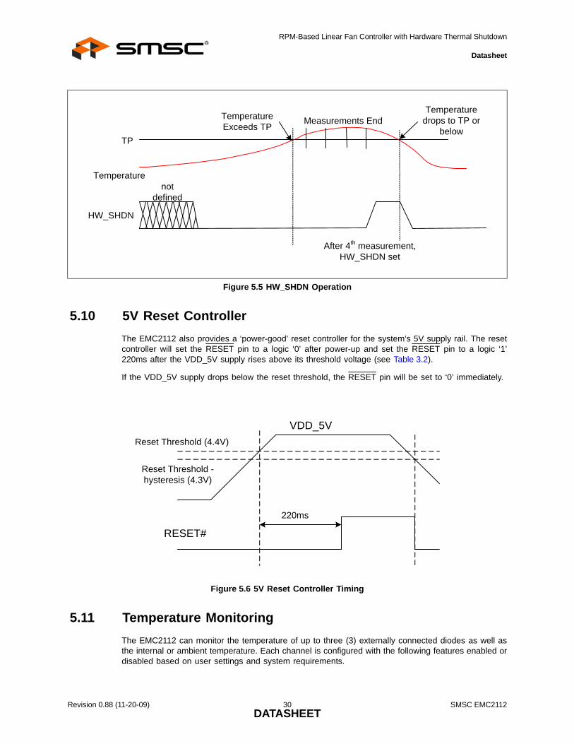
5.10 5V Reset Controller The EMC2112 also provides a ‘power-good’ reset controller for the system’s 5V supply rail. The resetcontroller will set the RESET pin to a logic ‘0’ after power-up and set the RESET pin to a logic ‘1’220ms after the VDD_5V supply rises above its threshold voltage (see Table 3.2).
If the VDD_5V supply drops below the reset threshold, the RESET pin will be set to ‘0’ immediately.
5.11 Temperature MonitoringThe EMC2112 can monitor the temperature of up to three (3) externally connected diodes as well asthe internal or ambient temperature. Each channel is configured with the following features enabled ordisabled based on user settings and system requirements.
Figure 5.5 HW_SHDN Operation
Figure 5.6 5V Reset Controller Timing
TP
Temperature
HW_SHDN
not defined
Temperature Exceeds TP
Temperature drops to TP or
belowMeasurements End
After 4th measurement, HW_SHDN set
VDD_5VReset Threshold (4.4V)
Reset Threshold - hysteresis (4.3V)
RESET#
220ms
Revision 0.88 (11-20-09) 30 SMSC EMC2112DATASHEET

RPM-Based Linear Fan Controller with Hardware Thermal Shutdown
Datasheet
5.11.1 Dynamic Averaging
The EMC2112 supports dynamic averaging. When enabled, this feature changes the conversion timefor all external diode channels based on the selected conversion rate. This essentially increases theaveraging factor as shown in Table 5.4. The benefits of Dynamic Averaging are improved noiserejection due to the longer integration time as well as less random variation on the temperaturemeasurement.
5.11.2 Resistance Error Correction
The EMC2112 includes active Resistance Error Correction to remove the effect of up to 100 ohms ofseries resistance. Without this automatic feature, voltage developed across the parasitic resistance inthe remote diode path causes the temperature to read higher than the true temperature is. The errorinduced by parasitic resistance is approximately +0.7°C per ohm. Sources of parasitic resistanceinclude bulk resistance in the remote temperature transistor junctions, series resistance in the CPU,and resistance in the printed circuit board traces and package leads. Resistance error correction in theEMC2112 eliminates the need to characterize and compensate for parasitic resistance in the remotediode path.
5.11.3 Beta Compensation
The forward current gain, or beta, of a transistor is not constant as emitter currents change. This betavariation causes the measured VBE (which is related to the collector current which, in turn, is relatedto beta) to shift in a way that is not predicted by the ratio of emitter currents being forced into thedevice. This shift cause an error in the temperature measurement. Compensating for this error is alsoknown as implementing the BJT or transistor model for temperature measurement.
For discrete transistors configured with the collector and base shorted together, the beta is generallysufficiently high such that the percent change in beta variation is very small. For example, a 10%variation in beta for two forced emitter currents with a transistor whose ideal beta is 50 would contributeapproximately 0.25°C error at 100°C. However for substrate transistors where the base-emitter junctionis used for temperature measurement and the collector is tied to the substrate, the proportional betavariation will cause large error. For example, a 10% variation in beta for two forced emitter currentswith a transistor whose ideal beta is 0.5 would contribute approximately 8.25°C error at 100°C.
The Beta Compensation circuitry in the EMC2112 corrects for this beta variation to eliminate any errorwhich would normally be induced. This Beta Compensation circuitry automatically detects the type ofdiode connected and adjusts the beta settings accordingly.
Table 5.4 Dynamic Averaging Behavior
CONVERSION RATE
AVERAGING FACTOR (RELATIVE TO 11-BIT CONVERSION) FOR EXTERNAL DIODE CHANNELS
DYNAMIC AVERAGING ENABLED
DYNAMIC AVERAGING DISABLED
1 / sec 8x 1x
2 / sec 4x 1x
4 / sec 2x 1x
8 / sec 1x 1x
SMSC EMC2112 31 Revision 0.88 (11-20-09)DATASHEET
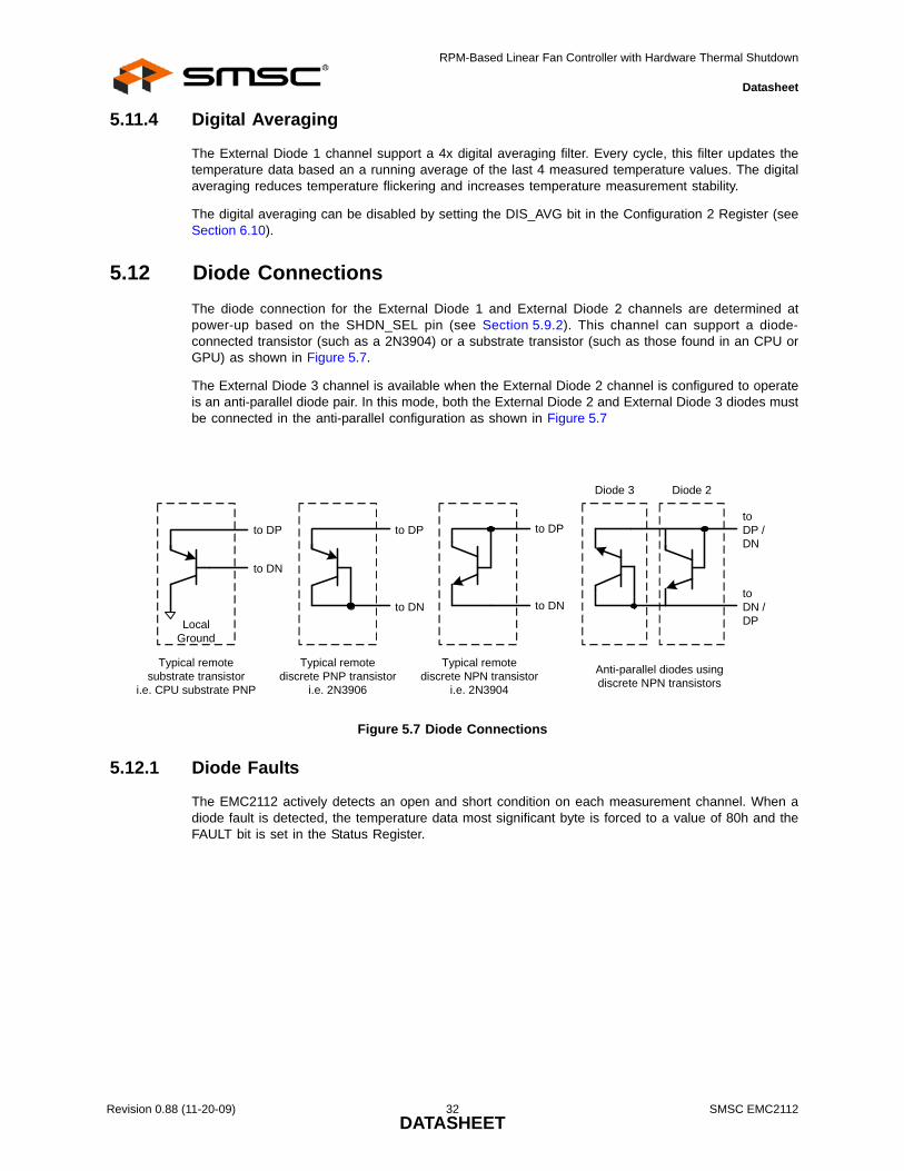
RPM-Based Linear Fan Controller with Hardware Thermal Shutdown
Datasheet
5.11.4 Digital Averaging
The External Diode 1 channel support a 4x digital averaging filter. Every cycle, this filter updates thetemperature data based an a running average of the last 4 measured temperature values. The digitalaveraging reduces temperature flickering and increases temperature measurement stability.
The digital averaging can be disabled by setting the DIS_AVG bit in the Configuration 2 Register (seeSection 6.10).
5.12 Diode ConnectionsThe diode connection for the External Diode 1 and External Diode 2 channels are determined atpower-up based on the SHDN_SEL pin (see Section 5.9.2). This channel can support a diode-connected transistor (such as a 2N3904) or a substrate transistor (such as those found in an CPU orGPU) as shown in Figure 5.7.
The External Diode 3 channel is available when the External Diode 2 channel is configured to operateis an anti-parallel diode pair. In this mode, both the External Diode 2 and External Diode 3 diodes mustbe connected in the anti-parallel configuration as shown in Figure 5.7
5.12.1 Diode Faults
The EMC2112 actively detects an open and short condition on each measurement channel. When adiode fault is detected, the temperature data most significant byte is forced to a value of 80h and theFAULT bit is set in the Status Register.
Figure 5.7 Diode Connections
Local Ground
to DP
Typical remote substrate transistor
i.e. CPU substrate PNP
Typical remote discrete PNP transistor
i.e. 2N3906
Typical remote discrete NPN transistor
i.e. 2N3904
to DN
to DP
to DN
to DP
to DN
to DP / DN
to DN / DP
Anti-parallel diodes using discrete NPN transistors
Diode 2Diode 3
Revision 0.88 (11-20-09) 32 SMSC EMC2112DATASHEET

RPM-Based Linear Fan Controller with Hardware Thermal Shutdown
Datasheet
Chapter 6 Register Set
6.1 Register MapThe following registers are accessible through the SMBus Interface. All register bits marked as ‘-’ willalways read ‘0’. A write to these bits will have no effect.
Table 6.1 EMC2112 Register Set
ADDR R/WREGISTER
NAME FUNCTIONDEFAULT
VALUE LOCK PAGE
Temperature Registers
00h RInternal Temp Reading High
Byte
Stores the integer data of the Internal Diode 00h No Page 36
01h R Internal Temp Reading Low Byte
Stores the fractional data of the Internal Diode 00h No Page 36
02h RExternal Diode 1 Temp Reading
High Byte
Stores the integer data of External Diode 1 channel 00h No Page 36
03h RExternal Diode 1 Temp Reading
Low Byte
Stores the fractional data of External Diode 1 00h No Page 36
04h RExternal Diode 2 Temp Reading
High Byte
Stores the integer data of External Diode 2 channel 00h No Page 36
05h RExternal Diode 2 Temp Reading
Low Byte
Stores the fractional data of External Diode 2 00h No Page 36
06h RExternal Diode 3 Temp Reading
High Byte
Stores the integer data of External Diode 3 channel 00h No Page 36
07h RExternal Diode 3 Temp Reading
Low Byte
Stores the fractional data of External Diode 3 00h No Page 36
0Ah RCritical/Thermal
Shutdown Temperature
Stores the calculated Critical/Thermal Shutdown temperature high limit
derived from the voltage on TRIP_SET
7Fh(+127°C) No Page 37
10h R Trip Set Voltage Stores the raw measured TRIP_SET voltage input FFh No Page 38
Diode Configuration
11h R/W External Diode 1 Ideality
Configures Ideality Factor settings for External Diode 1 12h SWL Page 38
12h R/W External Diode 2 Ideality
Configures Ideality Factor settings for External Diode 2 12h SWL Page 38
13h R/W External Diode 3 Ideality
Configures Ideality Factor settings for External Diode 3 12h SWL Page 38
SMSC EMC2112 33 Revision 0.88 (11-20-09)DATASHEET
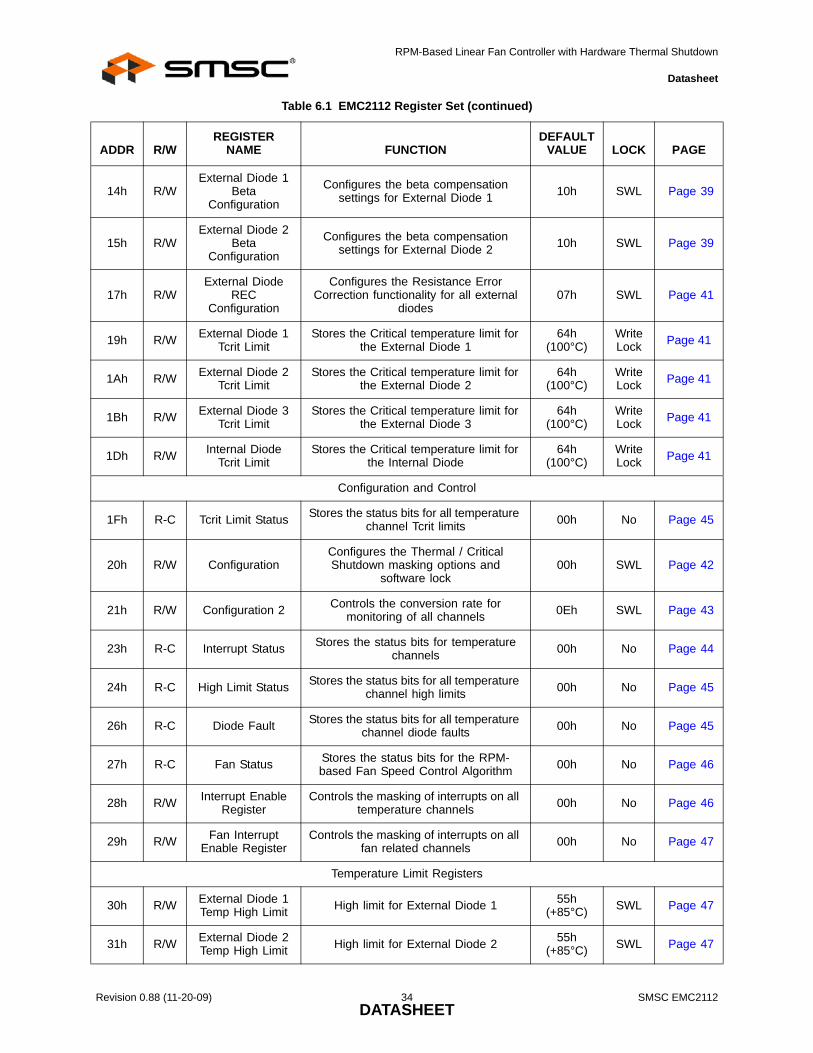
RPM-Based Linear Fan Controller with Hardware Thermal Shutdown
Datasheet
14h R/WExternal Diode 1
Beta Configuration
Configures the beta compensation settings for External Diode 1 10h SWL Page 39
15h R/WExternal Diode 2
Beta Configuration
Configures the beta compensation settings for External Diode 2 10h SWL Page 39
17h R/WExternal Diode
REC Configuration
Configures the Resistance Error Correction functionality for all external
diodes07h SWL Page 41
19h R/W External Diode 1 Tcrit Limit
Stores the Critical temperature limit for the External Diode 1
64h(100°C)
Write Lock Page 41
1Ah R/W External Diode 2 Tcrit Limit
Stores the Critical temperature limit for the External Diode 2
64h(100°C)
Write Lock Page 41
1Bh R/W External Diode 3 Tcrit Limit
Stores the Critical temperature limit for the External Diode 3
64h(100°C)
Write Lock Page 41
1Dh R/W Internal Diode Tcrit Limit
Stores the Critical temperature limit for the Internal Diode
64h(100°C)
Write Lock Page 41
Configuration and Control
1Fh R-C Tcrit Limit Status Stores the status bits for all temperature channel Tcrit limits 00h No Page 45
20h R/W ConfigurationConfigures the Thermal / Critical Shutdown masking options and
software lock00h SWL Page 42
21h R/W Configuration 2 Controls the conversion rate for monitoring of all channels 0Eh SWL Page 43
23h R-C Interrupt Status Stores the status bits for temperature channels 00h No Page 44
24h R-C High Limit Status Stores the status bits for all temperature channel high limits 00h No Page 45
26h R-C Diode Fault Stores the status bits for all temperature channel diode faults 00h No Page 45
27h R-C Fan Status Stores the status bits for the RPM-based Fan Speed Control Algorithm 00h No Page 46
28h R/W Interrupt Enable Register
Controls the masking of interrupts on all temperature channels 00h No Page 46
29h R/W Fan Interrupt Enable Register
Controls the masking of interrupts on all fan related channels 00h No Page 47
Temperature Limit Registers
30h R/W External Diode 1 Temp High Limit High limit for External Diode 1 55h
(+85°C) SWL Page 47
31h R/W External Diode 2 Temp High Limit High limit for External Diode 2 55h
(+85°C) SWL Page 47
Table 6.1 EMC2112 Register Set (continued)
ADDR R/WREGISTER
NAME FUNCTIONDEFAULT
VALUE LOCK PAGE
Revision 0.88 (11-20-09) 34 SMSC EMC2112DATASHEET

RPM-Based Linear Fan Controller with Hardware Thermal Shutdown
Datasheet
32h R/W External Diode 3 Temp High Limit High limit for External Diode 3 55h
(+85°C) SWL Page 47
34h R/W Internal Diode High Limit High Limit for Internal Diode 55h
(85°C) SWL Page 47
Fan Control Registers
40h R/W Fan Setting
Always displays the most recent fan driver input setting for the Fan. If the
RPM-based Fan Speed Control Algorithm is disabled, allows direct user
control of the fan driver.
00h No Page 48
42h R/W Fan Configuration 1
Sets configuration values for the RPM-based Fan Speed Control Algorithm for
the Fan driver2Bh No Page 48
43h R/W Fan Configuration 2
Sets additional configuration values for the Fan driver 28h SWL Page 50
45h R/W GainHolds the gain terms used by the RPM-based Fan Speed Control Algorithm for
the Fan driver2Ah SWL Page 51
46h R/W Fan Spin Up Configuration
Sets the configuration values for Spin Up Routine of the Fan driver 19h SWL Page 52
47h R/W Fan Step Sets the maximum change per update for the Fan driver 10h SWL Page 53
48h R/W Fan Minimum Drive
Sets the minimum drive value for the Fan driver
66h(40%) SWL Page 54
49h R/W Fan Valid TACH Count
Holds the minimum tachometer reading that indicates the fan is spinning
properlyF5h SWL Page 54
4Ah R/W Fan Drive Fail Band Low Byte Stores the number of Tach counts used
to determine how the actual fan speed must match the target fan speed at full
scale drive
00h SWLPage 55
4Bh R/W Fan Drive Fail Band High Byte 00h SWL
4Ch R/W TACH Target Low Byte
Holds the target tachometer reading low byte the Fan F8h No Page 55
4Dh R/W TACH Target High Byte
Holds the target tachometer reading high byte for the Fan FFh No Page 55
4Eh R TACH Reading High Byte
Holds the tachometer reading high byte for the Fan FFh No Page 55
4Fh R TACH Reading Low Byte
Holds the tachometer reading low byte for the Fan F8h No Page 55
Lock Register
EF R/W Software Lock Locks all SWL registers 00h SWL Page 56
Table 6.1 EMC2112 Register Set (continued)
ADDR R/WREGISTER
NAME FUNCTIONDEFAULT
VALUE LOCK PAGE
SMSC EMC2112 35 Revision 0.88 (11-20-09)DATASHEET

RPM-Based Linear Fan Controller with Hardware Thermal Shutdown
Datasheet
During Power-On-Reset (POR), the default values are stored in the registers. A POR is initiated whenpower is first applied to the part and the voltage on the VDD_3V supply surpasses the POR level asspecified in the electrical characteristics. Any reads to undefined registers will return 00h. Writes toundefined registers will not have an effect.
6.1.1 Lock Entries
The Lock Column describes the locking mechanism, if any, used for individual registers. All SWLregisters are Software Locked and therefore made read-only when the LOCK bit is set.
6.2 Temperature Data Registers
Revision Registers
FCh R Product Features Stores information about which pin controlled product features are set 00h No Page 57
FDh R Product ID Stores the unique Product ID 15h No Page 57
FEh R Manufacturer ID Stores the Manufacturer ID 5Dh No Page 58
FFh R Revision Revision 01h No Page 58
Table 6.2 Temperature Data Registers
ADDR R/W REGISTER B7 B6 B5 B4 B3 B2 B1 B0 DEFAULT
00h R Internal Diode High Byte Sign 64 32 16 8 4 2 1 00h
01h R Internal Diode Low Byte 0.5 0.25 0.125 - - - - - 00h
02h RExternal
Diode 1 High Byte
Sign 64 32 16 8 4 2 1 00h
03h RExternal
Diode 1 Low Byte
0.5 0.25 0.125 - - - - - 00h
04h RExternal
Diode 2 High Byte
Sign 64 32 16 8 4 2 1 00h
05h RExternal
Diode 2 Low Byte
0.5 0.25 0.125 - - - - - 00h
06h RExternal
Diode 3 High Byte
Sign 64 32 16 8 4 2 1 00h
07h RExternal
Diode 3 Low Byte
0.5 0.25 0.125 - - - - - 00h
Table 6.1 EMC2112 Register Set (continued)
ADDR R/WREGISTER
NAME FUNCTIONDEFAULT
VALUE LOCK PAGE
Revision 0.88 (11-20-09) 36 SMSC EMC2112DATASHEET
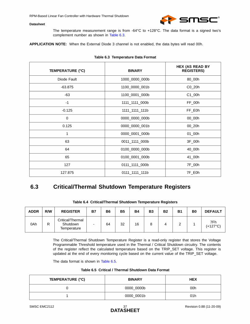
RPM-Based Linear Fan Controller with Hardware Thermal Shutdown
Datasheet
The temperature measurement range is from -64°C to +128°C. The data format is a signed two’scomplement number as shown in Table 6.3.
APPLICATION NOTE: When the External Diode 3 channel is not enabled, the data bytes will read 00h.
6.3 Critical/Thermal Shutdown Temperature Registers
The Critical/Thermal Shutdown Temperature Register is a read-only register that stores the VoltageProgrammable Threshold temperature used in the Thermal / Critical Shutdown circuitry. The contentsof the register reflect the calculated temperature based on the TRIP_SET voltage. This register isupdated at the end of every monitoring cycle based on the current value of the TRIP_SET voltage.
The data format is shown in Table 6.5.
Table 6.3 Temperature Data Format
TEMPERATURE (°C) BINARY HEX (AS READ BY
REGISTERS)
Diode Fault 1000_0000_000b 80_00h
-63.875 1100_0000_001b C0_20h
-63 1100_0001_000b C1_00h
-1 1111_1111_000b FF_00h
-0.125 1111_1111_111b FF_E0h
0 0000_0000_000b 00_00h
0.125 0000_0000_001b 00_20h
1 0000_0001_000b 01_00h
63 0011_1111_000b 3F_00h
64 0100_0000_000b 40_00h
65 0100_0001_000b 41_00h
127 0111_1111_000b 7F_00h
127.875 0111_1111_111b 7F_E0h
Table 6.4 Critical/Thermal Shutdown Temperature Registers
ADDR R/W REGISTER B7 B6 B5 B4 B3 B2 B1 B0 DEFAULT
0Ah RCritical/Thermal
Shutdown Temperature
- 64 32 16 8 4 2 1 7Fh(+127°C)
Table 6.5 Critical / Thermal Shutdown Data Format
TEMPERATURE (°C) BINARY HEX
0 0000_0000b 00h
1 0000_0001b 01h
SMSC EMC2112 37 Revision 0.88 (11-20-09)DATASHEET
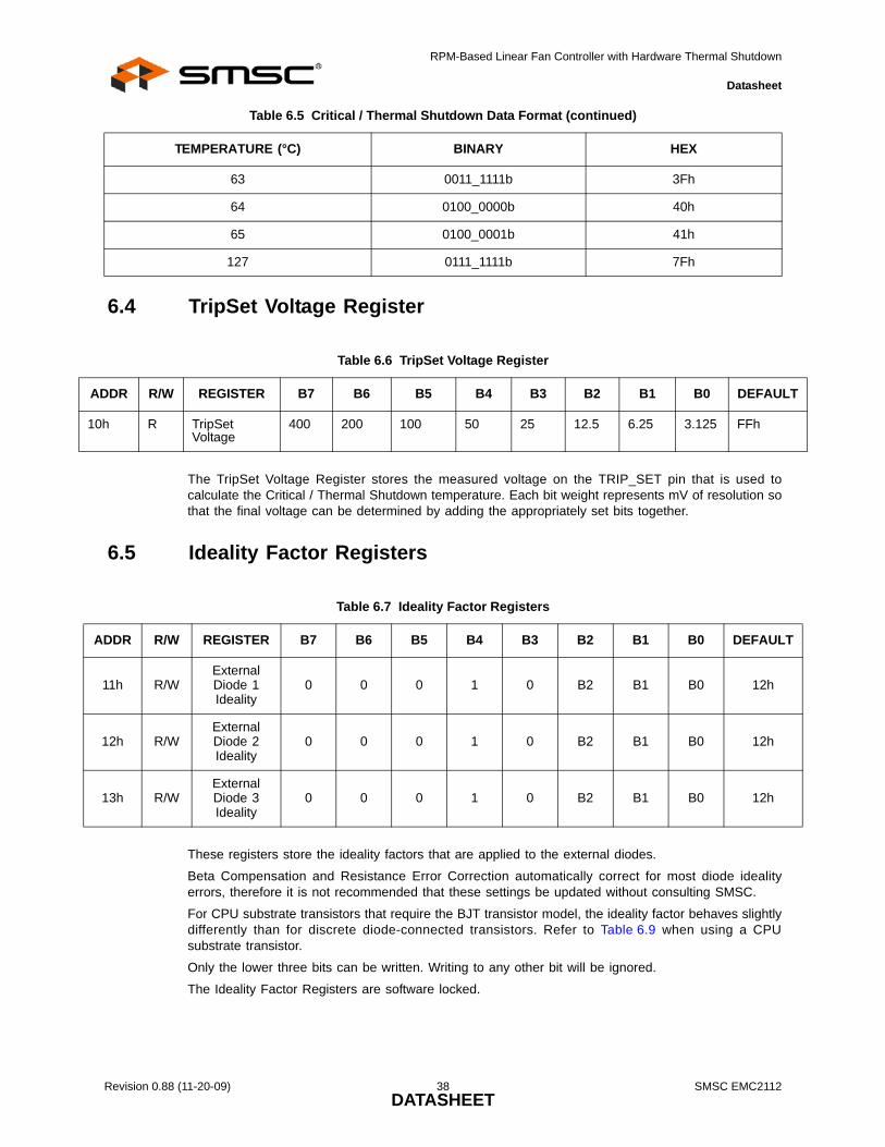
RPM-Based Linear Fan Controller with Hardware Thermal Shutdown
Datasheet
A
1
6.4 TripSet Voltage Register
The TripSet Voltage Register stores the measured voltage on the TRIP_SET pin that is used tocalculate the Critical / Thermal Shutdown temperature. Each bit weight represents mV of resolution sothat the final voltage can be determined by adding the appropriately set bits together.
6.5 Ideality Factor Registers
These registers store the ideality factors that are applied to the external diodes.
Beta Compensation and Resistance Error Correction automatically correct for most diode idealityerrors, therefore it is not recommended that these settings be updated without consulting SMSC.
For CPU substrate transistors that require the BJT transistor model, the ideality factor behaves slightlydifferently than for discrete diode-connected transistors. Refer to Table 6.9 when using a CPUsubstrate transistor.
Only the lower three bits can be written. Writing to any other bit will be ignored.
The Ideality Factor Registers are software locked.
63 0011_1111b 3Fh
64 0100_0000b 40h
65 0100_0001b 41h
127 0111_1111b 7Fh
Table 6.6 TripSet Voltage Register
DDR R/W REGISTER B7 B6 B5 B4 B3 B2 B1 B0 DEFAULT
0h R TripSet Voltage
400 200 100 50 25 12.5 6.25 3.125 FFh
Table 6.7 Ideality Factor Registers
ADDR R/W REGISTER B7 B6 B5 B4 B3 B2 B1 B0 DEFAULT
11h R/WExternal Diode 1 Ideality
0 0 0 1 0 B2 B1 B0 12h
12h R/WExternal Diode 2 Ideality
0 0 0 1 0 B2 B1 B0 12h
13h R/WExternal Diode 3 Ideality
0 0 0 1 0 B2 B1 B0 12h
Table 6.5 Critical / Thermal Shutdown Data Format (continued)
TEMPERATURE (°C) BINARY HEX
Revision 0.88 (11-20-09) 38 SMSC EMC2112DATASHEET
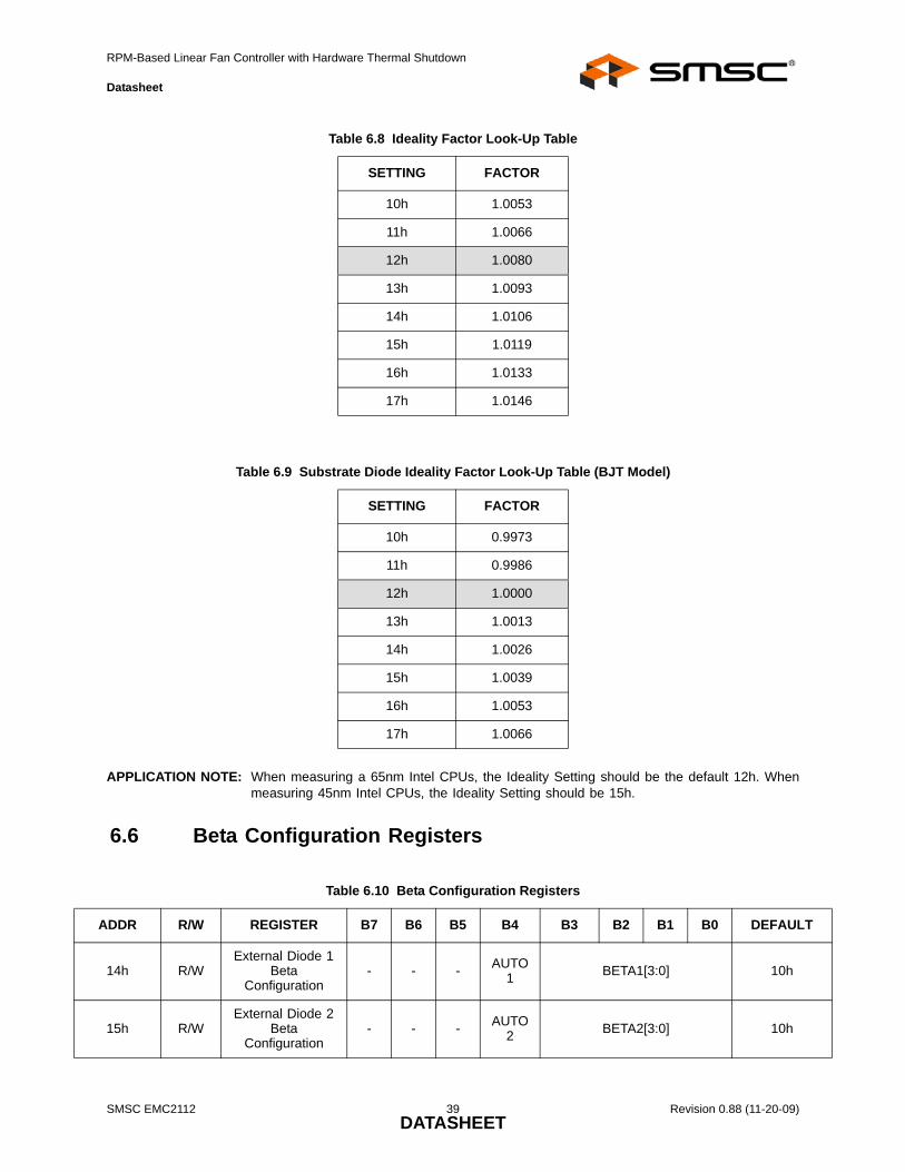
RPM-Based Linear Fan Controller with Hardware Thermal Shutdown
Datasheet
APPLICATION NOTE: When measuring a 65nm Intel CPUs, the Ideality Setting should be the default 12h. Whenmeasuring 45nm Intel CPUs, the Ideality Setting should be 15h.
6.6 Beta Configuration Registers
Table 6.8 Ideality Factor Look-Up Table
SETTING FACTOR
10h 1.0053
11h 1.0066
12h 1.0080
13h 1.0093
14h 1.0106
15h 1.0119
16h 1.0133
17h 1.0146
Table 6.9 Substrate Diode Ideality Factor Look-Up Table (BJT Model)
SETTING FACTOR
10h 0.9973
11h 0.9986
12h 1.0000
13h 1.0013
14h 1.0026
15h 1.0039
16h 1.0053
17h 1.0066
Table 6.10 Beta Configuration Registers
ADDR R/W REGISTER B7 B6 B5 B4 B3 B2 B1 B0 DEFAULT
14h R/WExternal Diode 1
Beta Configuration
- - - AUTO1 BETA1[3:0] 10h
15h R/WExternal Diode 2
Beta Configuration
- - - AUTO2 BETA2[3:0] 10h
SMSC EMC2112 39 Revision 0.88 (11-20-09)DATASHEET
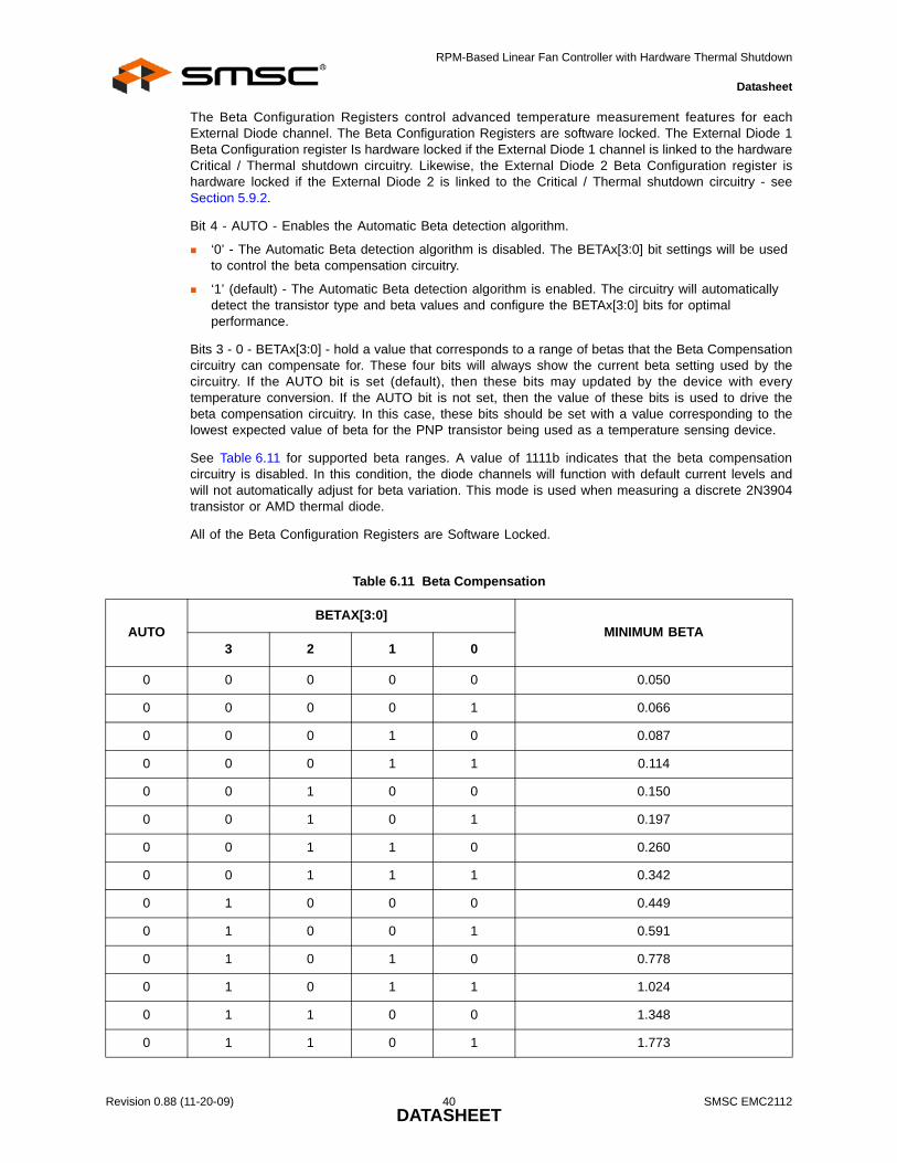
RPM-Based Linear Fan Controller with Hardware Thermal Shutdown
Datasheet
The Beta Configuration Registers control advanced temperature measurement features for eachExternal Diode channel. The Beta Configuration Registers are software locked. The External Diode 1Beta Configuration register Is hardware locked if the External Diode 1 channel is linked to the hardwareCritical / Thermal shutdown circuitry. Likewise, the External Diode 2 Beta Configuration register ishardware locked if the External Diode 2 is linked to the Critical / Thermal shutdown circuitry - seeSection 5.9.2.
Bit 4 - AUTO - Enables the Automatic Beta detection algorithm.
‘0’ - The Automatic Beta detection algorithm is disabled. The BETAx[3:0] bit settings will be used to control the beta compensation circuitry.
‘1’ (default) - The Automatic Beta detection algorithm is enabled. The circuitry will automatically detect the transistor type and beta values and configure the BETAx[3:0] bits for optimal performance.
Bits 3 - 0 - BETAx[3:0] - hold a value that corresponds to a range of betas that the Beta Compensationcircuitry can compensate for. These four bits will always show the current beta setting used by thecircuitry. If the AUTO bit is set (default), then these bits may updated by the device with everytemperature conversion. If the AUTO bit is not set, then the value of these bits is used to drive thebeta compensation circuitry. In this case, these bits should be set with a value corresponding to thelowest expected value of beta for the PNP transistor being used as a temperature sensing device.
See Table 6.11 for supported beta ranges. A value of 1111b indicates that the beta compensationcircuitry is disabled. In this condition, the diode channels will function with default current levels andwill not automatically adjust for beta variation. This mode is used when measuring a discrete 2N3904transistor or AMD thermal diode.
All of the Beta Configuration Registers are Software Locked.
Table 6.11 Beta Compensation
AUTOBETAX[3:0]
MINIMUM BETA3 2 1 0
0 0 0 0 0 0.050
0 0 0 0 1 0.066
0 0 0 1 0 0.087
0 0 0 1 1 0.114
0 0 1 0 0 0.150
0 0 1 0 1 0.197
0 0 1 1 0 0.260
0 0 1 1 1 0.342
0 1 0 0 0 0.449
0 1 0 0 1 0.591
0 1 0 1 0 0.778
0 1 0 1 1 1.024
0 1 1 0 0 1.348
0 1 1 0 1 1.773
Revision 0.88 (11-20-09) 40 SMSC EMC2112DATASHEET
RPM-Based Linear Fan Controller with Hardware Thermal Shutdown
Datasheet
A
1
A
6.7 REC Configuration Register
The REC Configuration Register determines whether Resistance Error Correction is used for eachexternal diode channel. The REC Configuration Register is software locked.
If either the External Diode 1 channel or External Diode 2 channel is selected by the SHDN_SEL pinto be the hardware shutdown input channel (see Table 5.3), then the corresponding RECx bit will belocked. Writing to the bit will have no affect and reading from it will always report the current setting.
Bit 2 - REC3 - Controls the Resistive Error Correction functionality of External Diode 3
‘0’ - the REC functionality for External Diode 3 is disabled
‘1’ (default) - the REC functionality for External Diode 3 is enabled.
Bit 1 - REC2 - Controls the Resistive Error Correction functionality of External Diode 2
‘0’ - the REC functionality for External Diode 2 is disabled
‘1’ (default) - the REC functionality for External Diode 2 is enabled.
Bit 0 - REC1 - Controls the Resistive Error Correction functionality of External Diode 1
‘0’ - the REC functionality for External Diode 1 is disabled
‘1’ (default) - the REC functionality for External Diode 1 is enabled.
6.8 Critical Temperature Limit Registers
0 1 1 1 0 2.333
0 1 1 1 1 Disabled
1 X X X X Automatically detected
Table 6.12 REC Configuration Register
DDRESS R/W REGISTER B7 B6 B5 B4 B3 B2 B1 B0 DEFAULT
7h R/W REC Configuration
- - - - - REC3 REC2 REC1 07h
Table 6.13 Tcrit Limit Registers
DDR R/W REGISTER B7 B6 B5 B4 B3 B2 B1 B0 DEFAULT
19h R/W once
External Diode 1 Tcrit Limit Sign 64 32 16 8 4 2 1 64h
(+100°C)
1Ah R/W once
External Diode 2 Tcrit Limit Sign 64 32 16 8 4 2 1 64h
(+100°C)
Table 6.11 Beta Compensation (continued)
AUTOBETAX[3:0]
MINIMUM BETA3 2 1 0
SMSC EMC2112 41 Revision 0.88 (11-20-09)DATASHEET

RPM-Based Linear Fan Controller with Hardware Thermal Shutdown
Datasheet
ADD LT
20h
A
The Critical Temperature Limit Registers store the Critical Temperature Limit. At power up, none of therespective channels are linked to Hardware set Thermal/Critical Shutdown circuitry.
Whenever one of the registers is updated, two things occur. First, the register is locked so that it cannotbe updated again without a power on reset. Second, the respective temperature channel is linked tothe SYS_SHDN pin and the Hardware set Thermal/Critical Shutdown Circuitry. At this point, if themeasured temperature channel exceeds the Critical limit, the SYS_SHDN pin will be asserted, theappropriate bit set in the Tcrit Status Register, and the TCRIT bit in the Interrupt Status Register willbe set.
6.9 Configuration Register
The Configuration Register controls the basic functionality of the EMC2112. The bits are describedbelow. The Configuration Register is software locked.
Bit 7 - MASK - Blocks the ALERT pin from being asserted.
‘0’ (default) - The ALERT pin is unmasked. If any bit in either status register is set, the ALERT pins will be asserted (unless individually masked via the Mask Register)
‘1’ - The ALERT pin is masked and will not be asserted.
Bit 6 - WD_EN - Enables the Watchdog timer to operate in Continuous Mode (see Section 5.6.2).
‘0’ (default) - The Watchdog timer does not operate continuously. It will function upon power up and at no other time.
‘1’ - The Watchdog timer operates continuously as described in Section 5.6.
Bit 2 - DR_EXT_CLK - Enables the internal tachometer clock to be driven out on the CLK pin so thatmultiple devices can be synced to the same source.
‘0’ (default) - The CLK pin acts as a clock input.
‘1’ - The CLK pin acts as a clock output and is a push-pull driver.
Bit 1 - USE_EXT_CLK - Enables the EMC2112 to use a clock present on the CLK pin as thetachometer clock. If the DR_EXT_CLK bit is set, then this bit is ignored and the device will use theinternal oscillator.
‘0’ (default) - The EMC2112 will use its internal oscillator for all Tachometer measurements.
‘1’ - The EMC2112 will use the oscillator presented on the CLK pin for all Tachometer measurements.
1Bh R/W once
External Diode 2 Tcrit Limit Sign 64 32 16 8 4 2 1 64h
(+100°C)
1Dh R/W once
Internal Diode Tcrit Limit Sign 64 32 16 8 4 2 1 64h
(+100°C)
Table 6.14 Configuration Register
R R/W REGISTER B7 B6 B5 B4 B3 B2 B1 B0 DEFAU
R/W Configuration MASK WD_ EN - - -
DR_EXT_CLK
USE_EXT_CLK
APD00h
Table 6.13 Tcrit Limit Registers (continued)
DDR R/W REGISTER B7 B6 B5 B4 B3 B2 B1 B0 DEFAULT
Revision 0.88 (11-20-09) 42 SMSC EMC2112DATASHEET
RPM-Based Linear Fan Controller with Hardware Thermal Shutdown
Datasheet
Bit 0 - APD - Enables the External Diode 3 channel.
‘0’ (default) - The External Diode 3 channel is not enabled.
‘1’ - The External Diode 3 channel is enabled as an anti-parallel diode connected to DP2 / DN2 pins.
6.10 Configuration 2 Register
The Configuration 2 Register controls conversion rate of the temperature monitoring as well as thefault queue. This register is software locked.
Bit 6 - DIS_DYN - Disables the Dynamic Averaging Feature.
‘0’ (default) - The Dynamic Averaging function is enabled. The conversion time for all external diode temperature channels is scaled based on the chosen conversion rate to maximize accuracy and immunity to random temperature measurement variation.
‘1’ - The Dynamic Averaging function is disabled. The conversion time for all temperature channels is fixed regardless of the chosen conversion rate.
Bit 5 - DIS_TO - Disables the SMBus time out function for the SMBus client (if enabled).
‘0’ (default) - The SMBus timeout and idle functionality are enabled. The SMBus interface will time out if the clock line is held low for longer than 30ms. Likewise, it will reset if both the data and clock lines are held high for longer than 150us.
‘1’ - The SMBus timeout and idle functionality are disabled. The SMBus interface will not time out if the clock line is held low. Likewise, it will not reset if both the data and clock lines are held high for longer than 150us. This is used for I2C compliance.
Bit 4 - DIS_AVG - Disables digital averaging of the External Diode 1 channel.
‘0’ (default) - The External Diode 1 channel has digital averaging enabled. The temperature data is the average of the previous four measurements.
‘1’ - The External Diode 1 channel has digital averaging disabled. The temperature data is the last measured data.
Bits 3-2 - QUEUE[1:0] - Determines the number of consecutive out of limit conditions that arenecessary to trigger an interrupt. Each measurement channel has a separate fault queue associatedwith the high limit and diode fault condition except the internal diode.
The Critical / Thermal Shutdown temperature has a separate fault queue that applies to the selectedhardware shutdown channel (see Section 5.9) when compared against the threshold set by theTRIP_SET pin.
APPLICATION NOTE: If the fault queue for any channel is currently active (i.e. an out of limit condition has beendetected and caused the fault queue to increment) then changing the settings will not takeeffect until the fault queue is zeroed. This occurs by the ALERT pin asserting or the out oflimit condition being removed.
Table 6.15 Configuration 2 Register
ADDR R/W REGISTER B7 B6 B5 B4 B3 B2 B1 B0 DEFAULT
21h R/W Config 2 - DIS_DYN
DIS_TO
DIS_AVG QUEUE[1:0] CONV[1:0] 0Eh
SMSC EMC2112 43 Revision 0.88 (11-20-09)DATASHEET

RPM-Based Linear Fan Controller with Hardware Thermal Shutdown
Datasheet
A T
Bit 1 - 0 - CONV[1:0] - determines the conversion rate of the temperature monitoring. This conversionrate does not affect the fan driver. The supply current from VDD_3V is nominally dependent upon theconversion rate and the average current will increase as the conversion rate increases.
6.11 Interrupt Status Register
The Interrupt Status Register reports the operating condition of the EMC2112. If any of the bits are setto a logic ‘1’ (other than RESET and TSD), the ALERT pin will be asserted low if the correspondingchannel is enabled. If there are no set status bits, the ALERT pin will be released.
The bits that cause the ALERT pin to be asserted can be masked based on the channel they areassociated with unless stated otherwise.
Bit 7 - RESET - This bit is set to ‘1’ if the Reset Generator (see Section 5.10) has tripped, meaningthat the VDD_5V voltage level is less than its normal operating level (and the RESET pin is at a logic‘0’ state). This bit is cleared when the RESET output changes states to a logic ‘1’. This bit will notcause the ALERT pin to be asserted.
Table 6.16 Fault Queue
QUEUE[1:0]
NUMBER OF CONSECUTIVE OUT OF LIMIT CONDITIONS 1 0
0 0 1 (disabled)
0 1 2
1 0 3
1 1 4 (default)
Table 6.17 Conversion Rate
CONV[1:0]
CONVERSION RATE
TEMPERATURE OVER SAMPLING FROM 11 BITS
1 0 DYN_DIS = ‘0’ DYN_DIS = ‘1’
0 0 1 / sec x8 x1
0 1 2 / sec x4 x1
1 0 4 / sec (default) x2 x1
1 1 8 / sec x1 x1
Table 6.18 Interrupt Status Register
DDR R/W REGISTER B7 B6 B5 B4 B3 B2 B1 B0 DEFAUL
23h R-CInterrupt Status
Register RESET TSD TCRIT - FAN HIGH - FAULT 00h
Revision 0.88 (11-20-09) 44 SMSC EMC2112DATASHEET
RPM-Based Linear Fan Controller with Hardware Thermal Shutdown
Datasheet
AD T
1
2
2
Bit 6 - TSD - This bit is set to ‘1’ if the internal Thermal Shutdown (TSD) circuit trips indicating that thedie temperature has exceeded its threshold. When this bit is set, it will not cause the ALERT pin to beasserted however will coincide with the SYS_SHDN pin being asserted. This bit is cleared when theregister is read and the error condition has been removed.
Bit 5 - TCRIT - This bit is set to ‘1’ whenever the any bit in the Tcrit Status Register is set. This bit isautomatically cleared when the Tcrit Status Register is cleared.
Bit 3 - FAN - This bit is set to ‘1’ if any bit in the Fan Status Register is set. This bit is automaticallycleared when the Fan Status Register is read and the bits are cleared.
Bit 2 - HIGH - This bit is set to ‘1’ if any bit in the High Status Register is set. This bit is automaticallycleared when the High Status Register is read and the bits are cleared.
Bit 0 - FAULT - This bit is set to ‘1’ if any bit in the Diode Fault Register is set. This bit is automaticallycleared when the Diode Fault Register is read and the bits are cleared.
6.12 Error Status Registers
The Error Status Registers report the specific error condition for all measurement channels with limits.If any bit is set in the High, Low, or Diode Fault Status register, the corresponding High, Low, or Faultbit is set in the Interrupt Status Register.
Reading the Interrupt Status Register does not clear the Error Status bit. Reading from any Error StatusRegister that has bits set will clear the register and the corresponding bit in the Interrupt StatusRegister if the error condition has been removed. If the error condition is persistent, reading the ErrorStatus Registers will have no affect.
6.12.1 Tcrit Status Register
The Tcrit Status Register stores the event that caused the SYS_SHDN pin to be asserted. Each of thetemperature channels must be associated with the SYS_SHDN pin before the corresponding status bitcan be set (see Section 6.8). Once the SYS_SHDN pin is asserted, it will be released when thetemperature drops below the threshold level however the individual status bit will not be cleared untilread.
Bit 7 - HWS - This bit is set if the hardware set temperature channel meets or exceeds the temperaturethreshold determined by the TRIP_SET voltage.
Table 6.19 Error Status Register
DR R/W REGISTER B7 B6 B5 B4 B3 B2 B1 B0 DEFAUL
Fh R-C Tcrit Status HWS - - - EXT3_CRIT
EXT2_CRIT
EXT1_CRIT
INT_CRIT 00h
4h R-C High Status - - - - EXT3_HI
EXT2_HI
EXT1_HI
INT_HI 00h
6h R-C Diode Fault - - - - EXT3_FLT
EXT2_FLT
EXT1_FLT - 00h
SMSC EMC2112 45 Revision 0.88 (11-20-09)DATASHEET
RPM-Based Linear Fan Controller with Hardware Thermal Shutdown
Datasheet
ADDR FAULT
27h 00h
ADDR AULT
28 00h
6.13 Fan Status Register
The Fan Status Register contains the status bits associated with each fan driver. This register iscleared when read if the error condition has been removed.
Bit 7 - WATCH - This bit is asserted ‘1’ if the Watchdog timer has expired (see Section 5.6).
Bit 5 - DRIVE_FAIL - Indicates that the RPM-based Fan Speed Control Algorithm cannot drive the Fanto the desired target setting at maximum drive. This bit can be masked from asserting the ALERT pin.
‘0’ - The RPM-based Fan Speed Control Algorithm can drive the Fan to the desired target setting.
‘1’ - The RPM-based Fan Speed Control Algorithm cannot drive the Fan to the desired target setting at maximum drive.
Bit 4- FAN_SHORT - This bit is asserted ‘1’ if the High Side Fan Driver detects an over currentcondition that lasts for longer than 2 seconds.
Bit 1- FAN_SPIN- This bit is asserted ‘1’ if the Spin up Routine for the Fan cannot detect a validtachometer reading within its maximum time window. This bit can be masked from asserting the ALERTpin.
Bit 0 - FAN_STALL - This bit is asserted ‘1’ if the tachometer measurement on the Fan detects a stalledfan. This bit can be masked from asserting the ALERT pin.
6.14 Interrupt Enable Register
The Interrupt Enable Register controls the masking for each temperature channel. When a channel ismasked, it will not cause the ALERT pin to be asserted when an error condition is detected.
Bit 3 - EXT3_INT_EN - Allows the External Diode 3 channel to assert the ALERT pin. This bit can onlybe set if the APD bit is set.
‘0’ (default) - The ALERT pin will not be asserted for any error condition associated with External Diode 3 channel.
‘1’ - The ALERT pin will be asserted for an error condition associated with External Diode 3 channel.
Bit 2 - EXT2_INT_EN - Allows the External Diode 2 channel to assert the ALERT pin.
‘0’ (default) - The ALERT pin will not be asserted for any error condition associated with External Diode 2 channel.
‘1’ - The ALERT pin will be asserted for an error condition associated with External Diode 2 channel.
Table 6.20 Fan Status Register
R/W REGISTER B7 B6 B5 B4 B3 B2 B1 B0 DE
R-C Fan Status Register WATCH - DRIVE_
FAIL FAN_
SHORT - - FAN_ SPIN
FAN_ STALL
Table 6.21 Interrupt Enable Register
R/W REGISTER B7 B6 B5 B4 B3 B2 B1 B0 DEF
R/W Interrupt Enable - - - - EXT3_
INT_ENEXT2_INT_EN
EXT1_INT_EN
INT_INT_EN
Revision 0.88 (11-20-09) 46 SMSC EMC2112DATASHEET
RPM-Based Linear Fan Controller with Hardware Thermal Shutdown
Datasheet
ADD ULT
29h
A T
Bit 1 - EXT1_INT_EN - Allows the External Diode 1 channel to assert the ALERT pin.
‘0’ (default) - The ALERT pin will not be asserted for any error condition associated with External Diode 1 channel.
‘1’ - The ALERT pin will be asserted for an error condition associated with External Diode 1 channel.
Bit 0 - INT_INT_EN - Allows the Internal Diode channel to assert the ALERT pin.
‘0’ (default) - The ALERT pin will not be asserted for any error condition associated with the Internal Diode.
‘1’ - The ALERT pin will be asserted for an error condition associated with the Internal Diode.
6.15 Fan Interrupt Enable Register
The Fan Interrupt Enable controls the masking for each Fan channel. When a channel is enabled, itwill cause the ALERT pin to be asserted when an error condition is detected.
Bit 1 - SPIN_INT_EN - Allows the FAN_SPIN bit to assert the ALERT pin.
‘0’ (default) - the FAN_SPIN bit will not assert the ALERT pin though it will still update the Status Register normally.
‘1’ - the FAN_SPIN bit will assert the ALERT pin.
Bit 0 - STALL_INT_EN - Allows the FAN_STALL bit or DRIVE_FAIL bit to assert the ALERT pin.
‘0’ (default) - the FAN_STALL bit or DRIVE_FAIL bit will not assert the ALERT pin though will still update the Status Register normally.
‘1’ - the FAN_STALL or DRIVE_FAIL bit will assert the ALERT pin if set.
6.16 Limit Registers
Table 6.22 Fan Interrupt Enable Register
R R/W REGISTER B7 B6 B5 B4 B3 B2 B1 B0 DEFA
R/WFan
Interrupt Enable
- - - - - - SPIN_ INT_EN
STALL_INT_EN 00h
Table 6.23 Limit Registers
DDR R/W REGISTER B7 B6 B5 B4 B3 B2 B1 B0 DEFAUL
30h R/W External Diode 1 High Limit Sign 64 32 16 8 4 2 1 55h
(+85°C)
31h R/W External Diode 2 High Limit Sign 64 32 16 8 4 2 1 55h
(+85°C)
32h R/W External Diode 3 High Limit Sign 64 32 16 8 4 2 1 55h
(+85°C)
34h R/W Internal Diode High Limit Sign 64 32 16 8 4 2 1 55h
(+85°C)
SMSC EMC2112 47 Revision 0.88 (11-20-09)DATASHEET
RPM-Based Linear Fan Controller with Hardware Thermal Shutdown
Datasheet
The EMC2112 contains high limits for all temperature channels and voltage channels. If anymeasurement meets or exceeds the high limit then the appropriate status bit is set and the ALERT pinis asserted (if enabled).
All Limit Registers are Software Locked.
6.17 Fan Setting Register
The Fan Setting Register always displays the current setting of the Fan Driver. Reading from theregister will report the current fan speed setting of the fan driver regardless of the operating mode.Therefore it is possible that reading from this register will not report data that was previously writteninto this register.
While the RPM-based Fan Speed Control Algorithm is active, then the register is read only. Writing tothe register will have no affect and the data will not be stored.
If the RPM-based Fan Control Algorithm is disabled, then the register will be set with the previousvalue that was used. The register is read / write and writing to this register will affect the fan speed.
The contents of the register represent the weighting of each bit in determining the final output voltage.The output drive for the High Side Fan Driver output is given by Equation [2].
6.18 Fan Configuration 1 Register
The Fan Configuration 1 Register controls the general operation of the RPM-based Fan Speed ControlAlgorithm used for the Fan 1 driver.
Bit 7 - EN_ALGO - enables the RPM-based Fan Speed Control Algorithm.
‘0’ - (default) the control circuitry is disabled and the fan driver output is determined by the Fan Driver Setting Register.
‘1’ - the control circuitry is enabled and the Fan Driver output will be automatically updated to maintain the programmed fan speed as indicated by the TACH Target Register.
Bits 6- 5 - RANGE[1:0] - Adjusts the range of reported and programmed tachometer reading values.The RANGE bits determine the weighting of all TACH values (including the Valid TACH Count, TACHTarget, and TACH reading) as shown in Table 6.26.
Table 6.24 Fan Setting Register
ADDR R/W REGISTER B7 B6 B5 B4 B3 B2 B1 B0 DEFAULT
40h R/W Fan Setting 128 64 32 16 8 4 2 1 00h
[2]
Table 6.25 Fan Configuration 1 Register
ADDR R/W REGISTER B7 B6 B5 B4 B3 B2 B1 B0 DEFAULT
42h R/W Fan Configuration 1
EN_ ALGO RANGE[1:0] EDGES[1:0] UPDATE[2:0] 2Bh
Drive VALUE255
---------------------⎝ ⎠⎛ ⎞ VDD_5V×=
Revision 0.88 (11-20-09) 48 SMSC EMC2112DATASHEET
RPM-Based Linear Fan Controller with Hardware Thermal Shutdown
Datasheet
Bits 4-3 - EDGES[1:0] - determines the minimum number of edges that must be detected on the TACHsignal to determine a single rotation. A typical fan measured 5 edges (for a 2-pole fan). For moreaccurate tachometer measurement, the minimum number of edges measured may be increased.
Increasing the number of edges measured with respect to the number of poles of the fan will causethe TACH Reading registers to indicate a fan speed that is higher or lower than the actual speed. Inorder for the FSC Algorithm to operate correctly, the TACH Target must be updated by the user toaccommodate this shift. The Effective Tach Multiplier shown in Table 6.27 is used as a direct multiplierterm that is applied to the Actual RPM to achieve the Reported RPM. It should only be applied if thenumber of edges measured does not match the number of edges expected based on the number ofpoles of the fan (which is fixed for any given fan).
Contact SMSC for recommended settings when using fans with more or less than 2 poles.
Bit 2-0 - UPDATE - determines the base time between fan driver updates. The Update Time, alongwith the Fan Step Register, is used to control the ramp rate of the drive response to provide a cleanertransition of the actual fan operation as the desired fan speed changes. The Update Time is set asshown in Table 6.28.
Table 6.26 Range Decode
RANGE[1:0]REPORTED MINIMUM
RPMTACH COUNT MULTIPLIER
1 0
0 0 500 1
0 1 1000 (default) 2
1 0 2000 4
1 1 4000 8
Table 6.27 Minimum Edges for Fan Rotation
EDGES[1:0]MINIMUM TACH
EDGES NUMBER OF FAN POLESEFFECTIVE TACH
MULTIPLIER (BASED ON 2 POLE FANS)1 0
0 0 3 1 pole 0.5
0 1 5 2 poles (default) 1
1 0 7 3 poles 1.5
1 1 9 4 poles 2
Table 6.28 Update Time
UPDATE[2:0]UPDATE TIME
2 1 0
0 0 0 100ms
0 0 1 200ms
0 1 0 300ms
SMSC EMC2112 49 Revision 0.88 (11-20-09)DATASHEET

RPM-Based Linear Fan Controller with Hardware Thermal Shutdown
Datasheet
ADDR FAULT
43h 28h
6.19 Fan Configuration 2 Register
The Fan Configuration 2 Register controls the tachometer measurement and advanced features of theRPM-based Fan Speed Control Algorithm.
Bit 7 - TEMP_RR - Overrides max step controls for the FSC algorithm when any temperature exceedsits respective high limit.
‘0’ (default) - All ramp rate control circuitry works at all times for the FSC algorithm or as determined by the EN_RRC bit for manual mode.
‘1’ - If any measured temperature or the PWM Input Duty cycle meets or exceeds its respective high limit, then the Fan Max Step register settings are not used and the FSC algorithm acts as if the Max Step settings were at 3Fh. The device will continue to operate in this way until all temperatures (and the PWM input duty cycle) have dropped below the respective high limit.
Bit 6 - EN_RRC - Enables ramp rate control when the fan driver is operated in the Direct Setting Mode.
‘0’ (default) - Ramp rate control is disabled. When the fan driver is operating in Direct Setting mode, the fan setting will instantly transition to the next programmed setting.
‘1’ - Ramp rate control is enabled. When the fan driver is operating in Direct Setting mode, the fan drive setting will follow the ramp rate controls as determined by the Fan Step and Update Time settings. The maximum fan drive setting step is capped at the Fan Step setting and is updated based on the Update Time as given by Table 6.28.
Bit 5 - GLITCH_EN - Disables the low pass glitch filter that removes high frequency noise injected onthe TACH pin.
‘0’ - The glitch filter is disabled.
‘1’ (default) - The glitch filter is enabled.
Bits 4 - 3 - DER_OPT[1:0] - Control some of the advanced options that affect the derivative portion ofthe RPM-based Fan Speed Control Algorithm as shown in Table 6.30.
0 1 1 400ms (default)
1 0 0 500ms
1 0 1 800ms
1 1 0 1200ms
1 1 1 1600ms
Table 6.29 Fan Configuration 1 Register
R/W REGISTER B7 B6 B5 B4 B3 B2 B1 B0 DE
R/W Fan Configuration 2
TEMP_RR
EN_ RRC
GLITCH_EN DER_OPT [1:0] ERR_RNG[1:0] -
Table 6.28 Update Time (continued)
UPDATE[2:0]UPDATE TIME
2 1 0
Revision 0.88 (11-20-09) 50 SMSC EMC2112DATASHEET
RPM-Based Linear Fan Controller with Hardware Thermal Shutdown
Datasheet
Bit 2 - 1 - ERR_RNG[1:0] - Control some of the advanced options that affect the error window. Whenthe measured fan speed is within the programmed error window around the target speed, then the fandrive setting is not updated. The algorithm will continue to monitor the fan speed and calculatenecessary drive setting changes based on the error, however these changes are ignored.
6.20 Gain Register
The Gain Register stores the gain terms used by the proportional and integral portions of each of theRPM-based Fan Speed Control Algorithms. These gain terms are used as the KD, KI, and KP gainterms in a classic PID control solution.
Table 6.30 Derivative Options
DER_OPT[1:0]OPERATION
1 0
0 0 No derivative options used
0 1
Basic derivative. The derivative of the error from the current drive setting and the target is added to the iterative Fan Drive Register setting (in addition to proportional and
integral terms) (default)
1 0
Step derivative. The derivative of the error from the current drive setting and the target is added to the iterative Fan Drive Register setting and is not capped by the Fan Step Register. This allows faster response times than the
basic derivative.
1 1Both the basic derivative and the step derivative are used effectively causing the derivative term to have double the
effect of the derivative term.
Table 6.31 Error Range Options
ERR_RNG[1:0]OPERATION
1 0
0 0 0 RPM (default)
0 1 50 RPM
1 0 100 RPM
1 1 200 RPM
Table 6.32 Gain Register
ADDR R/W REGISTER B7 B6 B5 B4 B3 B2 B1 B0 DEFAULT
45h R/W Gain Register - - GAIND[1:0] GAINI[1:0] GAINP[1:0] 2Ah
SMSC EMC2112 51 Revision 0.88 (11-20-09)DATASHEET
RPM-Based Linear Fan Controller with Hardware Thermal Shutdown
Datasheet
6.21 Fan Spin Up Configuration Register
The Fan Spin Up Configuration Register controls the settings of Spin Up Routine. The Fan Spin UpConfiguration Register is software locked.
Bit 7 - 6 - DRIVE_FAIL_CNT[1:0] - Determines how many update cycles are used for the Drive Faildetection function as shown in Table 6.35. This circuitry determines whether the fan can be driven tothe desired tach target.
Bit 5 - NOKICK - Determines if the Spin Up Routine will drive the fan to 100% duty cycle for 1/4 of theprogrammed spin up time before driving it at the programmed level.
‘0’ (default) - The Spin Up Routine will drive the fan driver to 100% for 1/4 of the programmed spin up time before reverting to the programmed spin level.
‘1’ - The Spin Up Routine will not drive the fan driver to 100%. It will set the drive at the programmed spin level for the entire duration of the programmed spin up time.
Table 6.33 Gain Decode
GAIND OR GAINP OR GAINI [1:0]RESPECTIVE GAIN FACTOR
1 0
0 0 1x
0 1 2x
1 0 4x (default)
1 1 8x
Table 6.34 Fan Spin Up Configuration Register
ADDR R/W REGISTER B7 B6 B5 B4 B3 B2 B1 B0 DEFAULT
46h R/W Fan Spin Up Configuration
DRIVE_FAIL_CNT [1:0]
NOKICK SPIN_LVL[2:0] SPINUP_
TIME[1:0] 19h
Table 6.35 DRIVE_FAIL_CNT[1:0] Bit Decode
DRIVE_FAIL_CNT[1:0]NUMBER OF UPDATE PERIODS
1 0
0 0 Disabled - the Drive Fail detection circuitry is disabled (default)
0 1 16 - the Drive Fail detection circuitry will count for 16 update periods
1 0 32 - the Drive Fail detection circuitry will count for 32 update periods
1 1 64 - the Drive Fail detection circuitry will count for 64 update periods
Revision 0.88 (11-20-09) 52 SMSC EMC2112DATASHEET

RPM-Based Linear Fan Controller with Hardware Thermal Shutdown
Datasheet
Bits 4 - 2 - SPIN_LVL[2:0] - Determines the final drive level that is used by the Spin Up Routine asshown in Table 6.36.
Bit 1 -0 - SPINUP_TIME[1:0] - determines the maximum Spin Time that the Spin Up Routine will runfor (see Section 5.2). If a valid tachometer measurement is not detected before the Spin Time haselapsed, then an interrupt will be generated. When the RPM-based Fan Speed Control Algorithm isactive, the fan driver will attempt to re-start the fan immediately after the end of the last spin up attempt.
The Spin Time is set as shown in Table 6.37.
6.22 Fan Max Step Register
The Fan Max Step Register, along with the Update Time, controls the ramp rate of the fan driverresponse calculated by the RPM-based Fan Speed Control Algorithm. The value of the registersrepresents the maximum step size each fan driver will take between update times (see Section 6.18).
Table 6.36 Spin Level
SPIN_LVL[2:0]SPIN UP DRIVE LEVEL
2 1 0
0 0 0 30%
0 0 1 35%
0 1 0 40%
0 1 1 45%
1 0 0 50%
1 0 1 55%
1 1 0 60% (default)
1 1 1 65%
Table 6.37 Spin Time
SPINUP_TIME[1:0]TOTAL SPIN UP TIME
1 0
0 0 250 ms
0 1 500 ms (default)
1 0 1 sec
1 1 2 sec
Table 6.38 Fan Max Step Register
ADDR R/W REGISTER B7 B6 B5 B4 B3 B2 B1 B0 DEFAULT
47h R/W Fan Max Step - - 32 16 8 4 2 1 10h
SMSC EMC2112 53 Revision 0.88 (11-20-09)DATASHEET
RPM-Based Linear Fan Controller with Hardware Thermal Shutdown
Datasheet
ADD LT
48h %)
When the FSC algorithm is enabled, Ramp Rate control is automatically used. When the FSC is notactive, then Ramp Rate control can be enabled by asserting the EN_RRC bit (see Section 6.19)
APPLICATION NOTE: The UPDATE bits and Fan Step Register settings operate independently of the RPM-basedFan Speed Control Algorithm and will always limit the fan drive setting. That is, if theprogrammed fan drive setting (either in determined by the RPM-based Fan Speed ControlAlgorithm or by manual settings) exceeds the current fan drive setting by greater than theFan Step Register setting, the EMC2112 will limit the fan drive change to the value of theFan Step Register. It will use the Update Time to determine how often to update the drivesettings.
APPLICATION NOTE: If the Fan Speed Control Algorithm is used, the default settings in the Fan Configuration 2Register will cause the maximum fan step settings to be ignored.
The Fan Step Registers are software locked.
6.23 Fan Minimum Drive Register
The Fan Minimum Drive Register stores the minimum drive setting for each RPM-based Fan SpeedControl Algorithm. The RPM-based Fan Speed Control Algorithm will not drive the fan at a level lowerthan the minimum drive unless the target Fan Speed is set at FFh (see Section 6.26)
During normal operation, if the fan stops for any reason (including low drive), the RPM-based FanSpeed Control Algorithm will attempt to restart the fan. Setting the Fan Minimum Drive Registers to asetting that will maintain fan operation is a useful way to avoid potential fan oscillations as the controlcircuitry attempts to drive it at a level that cannot support fan operation.
The Fan Minimum Drive Register is software locked.
6.24 Valid TACH Count Register
The Valid TACH Count Register stores the maximum TACH Reading Register value to indicate thatthe each fan is spinning properly. The value is referenced at the end of the Spin Up Routine todetermine if the fan has started operating and decide if the device needs to retry. See Equation [3] fortranslating the count to an RPM. This register is only used when the FSC is active.
If the TACH Reading Register value exceeds the Valid TACH Count Register (indicating that the FanRPM is below the threshold set by this count), then a stalled fan is detected. In this condition, thealgorithm will automatically begin its Spin Up Routine.
If a TACH Target setting is set above the Valid TACH Count setting, then that setting will be ignoredand the algorithm will use the current fan drive setting.
The Valid TACH Count Register is software locked.
Table 6.39 Minimum Fan Drive Register
R R/W REGISTER B7 B6 B5 B4 B3 B2 B1 B0 DEFAU
R/W Fan Minimum Drive 128 64 32 16 8 4 2 1 66h (40
Table 6.40 Valid TACH Count Register
ADDR R/W REGISTER B7 B6 B5 B4 B3 B2 B1 B0 DEFAULT
49h R/W Valid TACH Count 4096 2048 1024 512 256 128 64 32 F5h
Revision 0.88 (11-20-09) 54 SMSC EMC2112DATASHEET
RPM-Based Linear Fan Controller with Hardware Thermal Shutdown
Datasheet
6.25 Fan Drive Fail Band Registers
The Fan Drive Fail Band Registers store the number of tach counts used by the Fan Drive Faildetection circuitry. This circuitry is activated when the fan drive setting high byte is at FFh. When it isenabled, the actual measured fan speed is compared against the target fan speed. These registersare only used when the FSC is active.
This circuitry is used to indicate that the target fan speed at full drive is higher than the fan is actuallycapable of reaching. If the measured fan speed does not exceed the target fan speed minus the FanDrive Fail Band Register settings for a period of time longer than set by the DRIVE_FAIL_CNTx[1:0]bits then the DRIVE_FAIL status bit will be set and an interrupt generated.
6.26 TACH Target Registers
The TACH Target Registers hold the target tachometer value that is maintained each of the RPM-based Fan Speed Control Algorithms.
If one of the algorithms is enabled then setting the TACH Target Register to FFh will disable the fandriver (set the fan drive setting to 0%). Setting the TACH Target to any other value (from a setting ofFFh) will cause the algorithm to invoke the Spin Up Routine after which it will function normally.
The Tach Target is not applied until the high byte is written. Once the high byte is written, the currentvalue of both high and low bytes will be used as the next Tach target. 3
6.27 TACH Reading Registers
Table 6.41 Fan Drive Fail Band Registers
ADDR R/W REGISTER B7 B6 B5 B4 B3 B2 B1 B0 DEFAULT
4Ah R/W Fan Drive Fail Band Low Byte 16 8 4 2 1 - - - 00h
4Bh R/W Fan Drive Fail Band High Byte 4096 2048 1024 512 256 128 64 32 00h
Table 6.42 TACH Target Registers
ADDR R/W REGISTER B7 B6 B5 B4 B3 B2 B1 B0 DEFAULT
4Ch R/W TACH Target Low Byte 16 8 4 2 1 - - - F8h
4Dh R/W TACH Target High Byte 4096 2048 1024 512 256 128 64 32 FFh
Table 6.43 TACH Reading Registers
ADDR R/W REGISTER B7 B6 B5 B4 B3 B2 B1 B0 DEFAULT
4Eh R Fan TACH 4096 2048 1024 512 256 128 64 32 FFh
4Fh R Fan TACH Low Byte 16 8 4 2 1 - - - F8h
SMSC EMC2112 55 Revision 0.88 (11-20-09)DATASHEET
RPM-Based Linear Fan Controller with Hardware Thermal Shutdown
Datasheet
AD LT
E
The TACH Reading Registers’ contents describe the current tachometer reading for each of the fan.By default, the data represents the fan speed as the number of 32kHz clock periods that occur for asingle revolution of the fan.
Equation [3] shows the detailed conversion from TACH measurement (COUNT) to RPM while Equation[4] shows the simplified translation of TACH Reading Register count to RPM assuming a 2-pole fan,measuring 5 edges, with a frequency of 32.768kHz. These equations are solved and tabulated for easeof use in AN17.4 RPM to TACH Counts Conversion.
Whenever the high byte register is read, the corresponding low byte data will be loaded to internalshadow registers so that when the low byte is read, the data will always coincide with the previouslyread high byte.
Bit 2 - IDCF_5 - Sets the bit state of IDCFx bit 5.
BIt 1 - IDCF_4 - Sets the bit state of IDCFx bit 4.
Bit 0 - IDCF_3 - Sets the bit state of IDCFx bit 3.
Prior to enabling the RUN_ALl bit, the TATRIM and TYPE[1:0] bits must be set to the desired settings.
6.28 Software Lock Register
The Software Lock Register controls the software locking of critical registers. This register is softwarelocked.
Bit 0 - LOCK - this bit acts on all registers that are designated SWL. When this bit is set, the lockedregisters become read only and cannot be updated.
‘0’ (default) - all SWL registers can be updated normally.
‘1’ - all SWL registers cannot be updated and a hard-reset is required to unlock them.
where:
[3]
poles = number of poles of the fan (typically 2)
fTACH = the tachometer measurement frequency (typically
32.768kHz)
n = number of edges measured (typically 5 for a 2 pole fan)
m = the multiplier defined by the RANGe bits
[4]COUNT = TACH Reading Register
value (in decimal)
Table 6.44 Software Lock Register
DR R/W REGISTER B7 B6 B5 B4 B3 B2 B1 B0 DEFAU
Fh R/W Software Lock - - - - - - - LOCK 00h
RPM 1poles( )
-------------------- n 1–( )
COUNT 1m-----×
---------------------------------- fTACH 60×××=
RPM 3,932,160 m×COUNT
--------------------------------------=
Revision 0.88 (11-20-09) 56 SMSC EMC2112DATASHEET

RPM-Based Linear Fan Controller with Hardware Thermal Shutdown
Datasheet
A
A T
6.29 Product Features Register
The Product Features register shows those functions that are enabled by external pin states.
Bits 3-2 - ADR[2:0] - Indicates the selected SMBus address as determined by the ADDR_SEL pin.
Bits 1-0 - SHDN_CH[1:0] - Indicates the selected temperature channel associated with the Critical /Thermal Shutdown logic (see Section 5.9).
6.30 Product ID Register
The Product ID Register contains a unique 8 bit word that identifies the product.
Table 6.45 Product Features Register
DDRESS R/W REGISTER B7 B6 B5 B4 B3 B2 B1 B0 DEFAULT
FCh R Product Features - - - - ADR[1:0] SHDN_CH
[1:0] 00h
Table 6.46 ADDR_SEL Pin Configuration
ADR[1:0]SLAVE ADDRESS
1 0
0 0 0101_111xb
0 1 0111_101xb
1 0 0101_110xb
Table 6.47 SHDN_CH Pin Configuration
SHDN_CH [1:0]HARDWARE SHUTDOWN CHANNEL
1 0
0 0 External Diode 1 measuring CPU / GPU diode
0 1 External Diode 1 measuring AMD or discrete diode
1 0 External Diode 2 measuring discrete diode
Table 6.48 Product ID Register
DDRESS R/W REGISTER B7 B6 B5 B4 B3 B2 B1 B0 DEFAUL
FDh R Product ID 0 0 0 1 0 1 0 1 15h
SMSC EMC2112 57 Revision 0.88 (11-20-09)DATASHEET
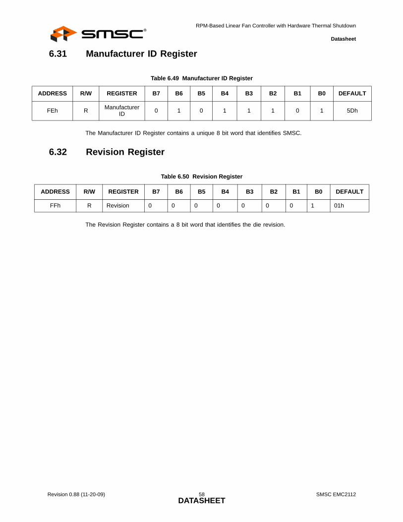
RPM-Based Linear Fan Controller with Hardware Thermal Shutdown
Datasheet
A T
A
6.31 Manufacturer ID Register
The Manufacturer ID Register contains a unique 8 bit word that identifies SMSC.
6.32 Revision Register
The Revision Register contains a 8 bit word that identifies the die revision.
Table 6.49 Manufacturer ID Register
DDRESS R/W REGISTER B7 B6 B5 B4 B3 B2 B1 B0 DEFAUL
FEh R Manufacturer ID 0 1 0 1 1 1 0 1 5Dh
Table 6.50 Revision Register
DDRESS R/W REGISTER B7 B6 B5 B4 B3 B2 B1 B0 DEFAULT
FFh R Revision 0 0 0 0 0 0 0 1 01h
Revision 0.88 (11-20-09) 58 SMSC EMC2112DATASHEET
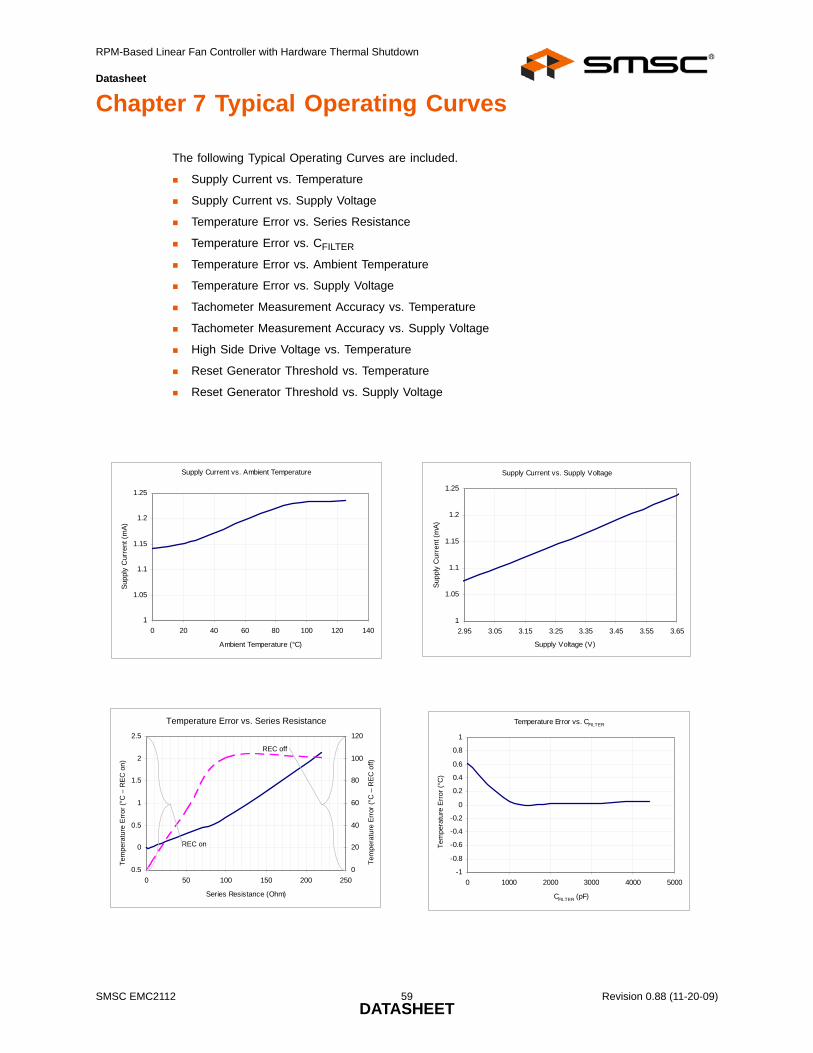
RPM-Based Linear Fan Controller with Hardware Thermal Shutdown
Datasheet
Chapter 7 Typical Operating Curves
The following Typical Operating Curves are included.
Supply Current vs. Temperature
Supply Current vs. Supply Voltage
Temperature Error vs. Series Resistance
Temperature Error vs. CFILTER
Temperature Error vs. Ambient Temperature
Temperature Error vs. Supply Voltage
Tachometer Measurement Accuracy vs. Temperature
Tachometer Measurement Accuracy vs. Supply Voltage
High Side Drive Voltage vs. Temperature
Reset Generator Threshold vs. Temperature
Reset Generator Threshold vs. Supply Voltage
Supply Current vs. Ambient Temperature
1
1.05
1.1
1.15
1.2
1.25
0 20 40 60 80 100 120 140
Ambient Temperature (°C)
Supp
ly C
urre
nt (m
A)
Supply Current vs. Supply Voltage
1
1.05
1.1
1.15
1.2
1.25
2.95 3.05 3.15 3.25 3.35 3.45 3.55 3.65
Supply Voltage (V)
Supp
ly C
urre
nt (m
A)
-0.5
0
0.5
1
1.5
2
2.5
0 50 100 150 200 250
Series Resistance (Ohm)
0
20
40
60
80
100
120
Tem
pera
ture
Err
or (°
C –
REC
on)
Tem
pera
ture
Err
or (°
C –
REC
off)
Temperature Error vs. Series Resistance
REC on
REC off
Temperature Error vs. CFILTER
-1
-0.8
-0.6
-0.4
-0.2
0
0.2
0.4
0.6
0.8
1
0 1000 2000 3000 4000 5000
CFILTER (pF)
Tem
pera
ture
Err
or (C
Tem
pera
ture
Erro
r (°C
)
SMSC EMC2112 59 Revision 0.88 (11-20-09)DATASHEET
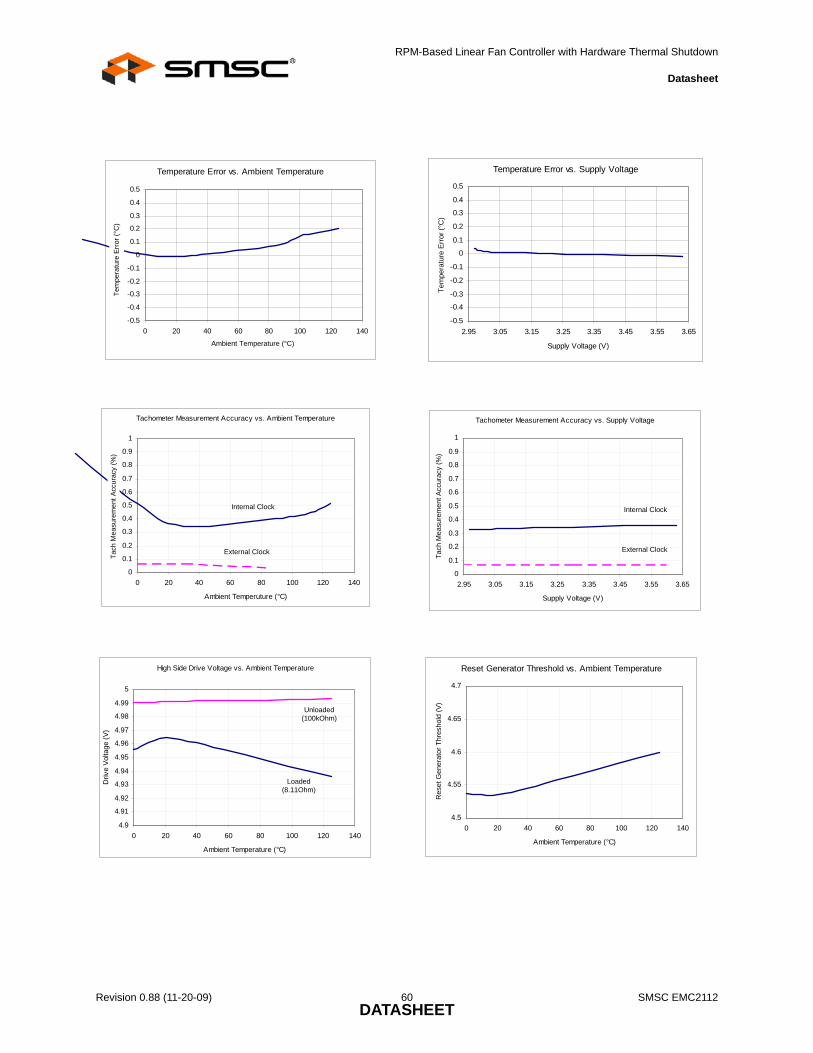
RPM-Based Linear Fan Controller with Hardware Thermal Shutdown
Datasheet
Temperature Error vs. Ambient Temperature
-0.5
-0.4
-0.3
-0.2
-0.1
0
0.1
0.2
0.3
0.4
0.5
0 20 40 60 80 100 120 140
Ambient Temperature (°C)
Tem
pera
ture
Err
or (°
CTe
mpe
ratu
re E
rror
(°C
)
Ambient Temperature (°C)
Temperature Error vs. Supply Voltage
-0.5
-0.4
-0.3
-0.2
-0.1
0
0.1
0.2
0.3
0.4
0.5
2.95 3.05 3.15 3.25 3.35 3.45 3.55 3.65
Supply Voltage (V)
Tem
pera
ture
Err
or (°
CTe
mpe
ratu
re E
rror
(°C
)
Tachometer Measurement Accuracy vs. Ambient Temperature
0
0.1
0.2
0.3
0.4
0.5
0.6
0.7
0.8
0.9
1
0 20 40 60 80 100 120 140
Ambient Temperuture (°C)
Tach
Mea
sure
men
t Acc
urac
y (%
Internal Clock
External Clock
Tach
Mea
sure
men
t Acc
urac
y (%
)
Tachometer Measurement Accuracy vs. Supply Voltage
0
0.1
0.2
0.3
0.4
0.5
0.6
0.7
0.8
0.9
1
2.95 3.05 3.15 3.25 3.35 3.45 3.55 3.65
Supply Voltage (V)
Tach
Mea
sure
men
t Acc
urac
y (%
External Clock
Internal Clock
Tach
Mea
sure
men
t Acc
urac
y (%
)
High Side Drive Voltage vs. Ambient Temperature
4.9
4.91
4.92
4.93
4.94
4.95
4.96
4.97
4.98
4.99
5
0 20 40 60 80 100 120 140
Ambient Temperature (°C)
Driv
e Vo
ltage
(V)
Loaded (8.11Ohm)
Unloaded (100kOhm)
Reset Generator Threshold vs. Ambient Temperature
4.5
4.55
4.6
4.65
4.7
0 20 40 60 80 100 120 140
Ambient Temperature (°C)
Res
et G
ener
ator
Thr
esho
ld (V
)R
eset
Gen
erat
or T
hres
hold
(V)
Revision 0.88 (11-20-09) 60 SMSC EMC2112DATASHEET
RPM-Based Linear Fan Controller with Hardware Thermal Shutdown
Datasheet
Reset Generator Threshold vs. Supply Voltage
4.5
4.55
4.6
4.65
4.7
2.95 3.05 3.15 3.25 3.35 3.45 3.55 3.65
Supply Voltage (V)
Res
et G
ener
ator
Thr
esho
ld (V
Res
et G
ener
ator
Thr
esho
ld (V
)
SMSC EMC2112 61 Revision 0.88 (11-20-09)DATASHEET

RPM-Based Linear Fan Controller with Hardware Thermal Shutdown
Datasheet
Chapter 8 Package Outline
8.1 EMC2112 Package Drawings - 20-Pin QFN 4mm x 4mm
Figure 8.1 EMC2112 Package Drawing - 20-Pin QFN 4mm x 4mm
Revision 0.88 (11-20-09) 62 SMSC EMC2112DATASHEET
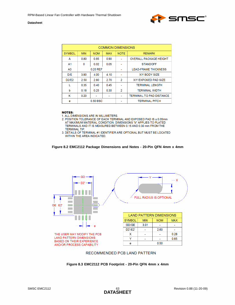
RPM-Based Linear Fan Controller with Hardware Thermal Shutdown
Datasheet
Figure 8.2 EMC2112 Package Dimensions and Notes - 20-Pin QFN 4mm x 4mm
Figure 8.3 EMC2112 PCB Footprint - 20-Pin QFN 4mm x 4mm
SMSC EMC2112 63 Revision 0.88 (11-20-09)DATASHEET
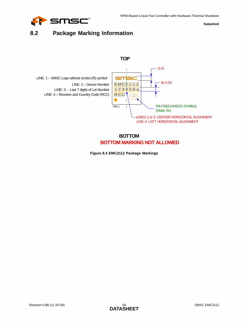
RPM-Based Linear Fan Controller with Hardware Thermal Shutdown
Datasheet
8.2 Package Marking Information
Figure 8.4 EMC2112 Package Markings
BOTTOMBOTTOM MARKING NOT ALLOWED
LINE: 1 – SMSC Logo without circled (R) symbol
LINE: 2 – Device NumberLINE: 3 – Last 7 digits of Lot Number
LINE: 4 – Revision and Country Code (RCC)
LINES 1 to 3: CENTER HORIZONTAL ALIGNMENTLINE 4: LEFT HORIZONTAL ALIGNMENT
PB-FREE/GREEN SYMBOL(Matte Sn)
0.41
3x 0.56
TOP
C 2ME 211
e3
PIN 1
C CR1 2 3 4 5 6 a
Revision 0.88 (11-20-09) 64 SMSC EMC2112DATASHEET
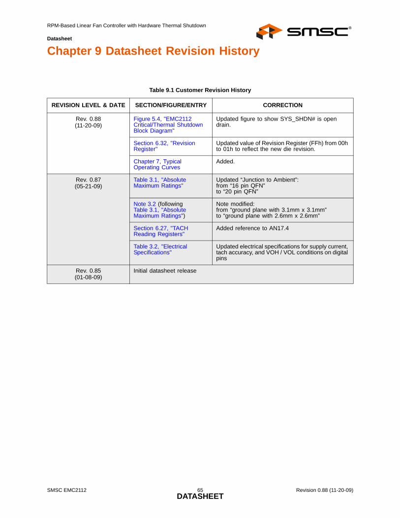
RPM-Based Linear Fan Controller with Hardware Thermal Shutdown
Datasheet
SMSC EMC2112 65 Revision 0.88 (11-20-09)DATASHEET
Chapter 9 Datasheet Revision History
Table 9.1 Customer Revision History
REVISION LEVEL & DATE SECTION/FIGURE/ENTRY CORRECTION
Rev. 0.88(11-20-09)
Figure 5.4, "EMC2112 Critical/Thermal Shutdown Block Diagram"
Updated figure to show SYS_SHDN# is open drain.
Section 6.32, "Revision Register"
Updated value of Revision Register (FFh) from 00h to 01h to reflect the new die revision.
Chapter 7, Typical Operating Curves
Added.
Rev. 0.87(05-21-09)
Table 3.1, "Absolute Maximum Ratings"
Updated “Junction to Ambient”: from “16 pin QFN” to “20 pin QFN”
Note 3.2 (following Table 3.1, "Absolute Maximum Ratings")
Note modified:from “ground plane with 3.1mm x 3.1mm” to “ground plane with 2.6mm x 2.6mm”
Section 6.27, "TACH Reading Registers"
Added reference to AN17.4
Table 3.2, "Electrical Specifications"
Updated electrical specifications for supply current, tach accuracy, and VOH / VOL conditions on digital pins
Rev. 0.85(01-08-09)
Initial datasheet release