EMC Design Guidelines - The Centre for Computing...
16
EMC Design Guidelines
Transcript of EMC Design Guidelines - The Centre for Computing...
EMC Design Guidelines
EMC Design Guidelines
Copyright (C) Acorn Computers Limited 1993
Published by Acorn Computers Technical Publications Department
Neither the whole nor any part of the information contained inthis manual may be adaptedor reproduced in any material form except with the prior written approval of Acorn Computers Limited:
Acorn Computers Limited cannot accept any liability for any loss or damage arising from the use of any information or particulars in this manual.
Published by Acorn Computers LtdPart No xxxxIssue B, May 1993
Issue B May 1993 (C) ACORN LTD V. Gibling ii
EMC Design Guidelines
Contents: page
Shielding:
Shielding efficiency 1Absorbtion loss 1Reflective loss 2Shield design 2
Design Features:The shape 3Electric Field Shielding Effectiveness Formula 3
Enclosure design:
Seams, interfaces , holes and slots 4Bonding 5Edge effects 5Cables and connectors 6Internal standing waves 6Plastic enclosures 6Metal enclosures 6
Summary of shielded enclosure design considerations
Selection of material 7Joins and seams 7Size of Holes/Slots 7Connector termination 7Star/Main Ground point 7Edge effect 7
EMC Design Guidelines for PCB layout 8
Issue B May 1993 (C) ACORN LTD V. Gibling iii
EMC Design GuidelinesShielding
The purpose of an enclosure in EMC terms is to provide a continuously closed conductive envelope in order to prevent outside fields from penetrating and internally generated noise from emerging. This is impractical as there is inevitably the need to pass power into the box, to communicate to other devices via cables and to ensure the circuitry within is adequately cooled: Each aperature made in the enclosure and any cable passing into or out from will reduce its shielding efficiency which will result in increased susceptibility and emissions.
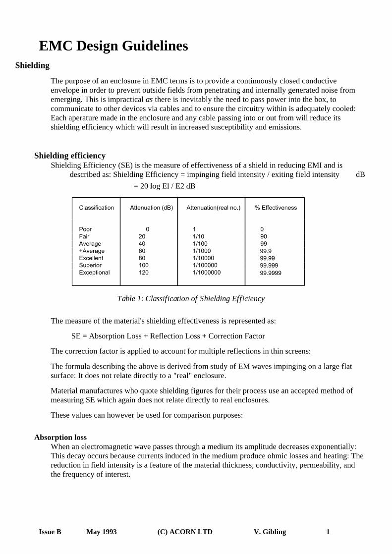
Shielding efficiencyShielding Efficiency (SE) is the measure of effectiveness of a shield in reducing EMI and is
described as: Shielding Efficiency = impinging field intensity / exiting field intensity dB
= 20 log El / E2 dB
Classification Attenuation (dB) Attenuation(real no.) % Effectiveness
Poor 0 1 0Fair 20 1/10 90Average 40 1/100 99+Average 60 1/1000 99.9Excellent 80 1/10000 99.99Superior 100 1/100000 99.999Exceptional 120 1/1000000 99.9999
Table 1: Classification of Shielding Efficiency
The measure of the material's shielding effectiveness is represented as:
SE = Absorption Loss + Reflection Loss + Correction Factor
The correction factor is applied to account for multiple reflections in thin screens:
The formula describing the above is derived from study of EM waves impinging on a large flat surface: It does not relate directly to a "real" enclosure.
Material manufactures who quote shielding figures for their process use an accepted method of measuring SE which again does not relate directly to real enclosures.
These values can however be used for comparison purposes:
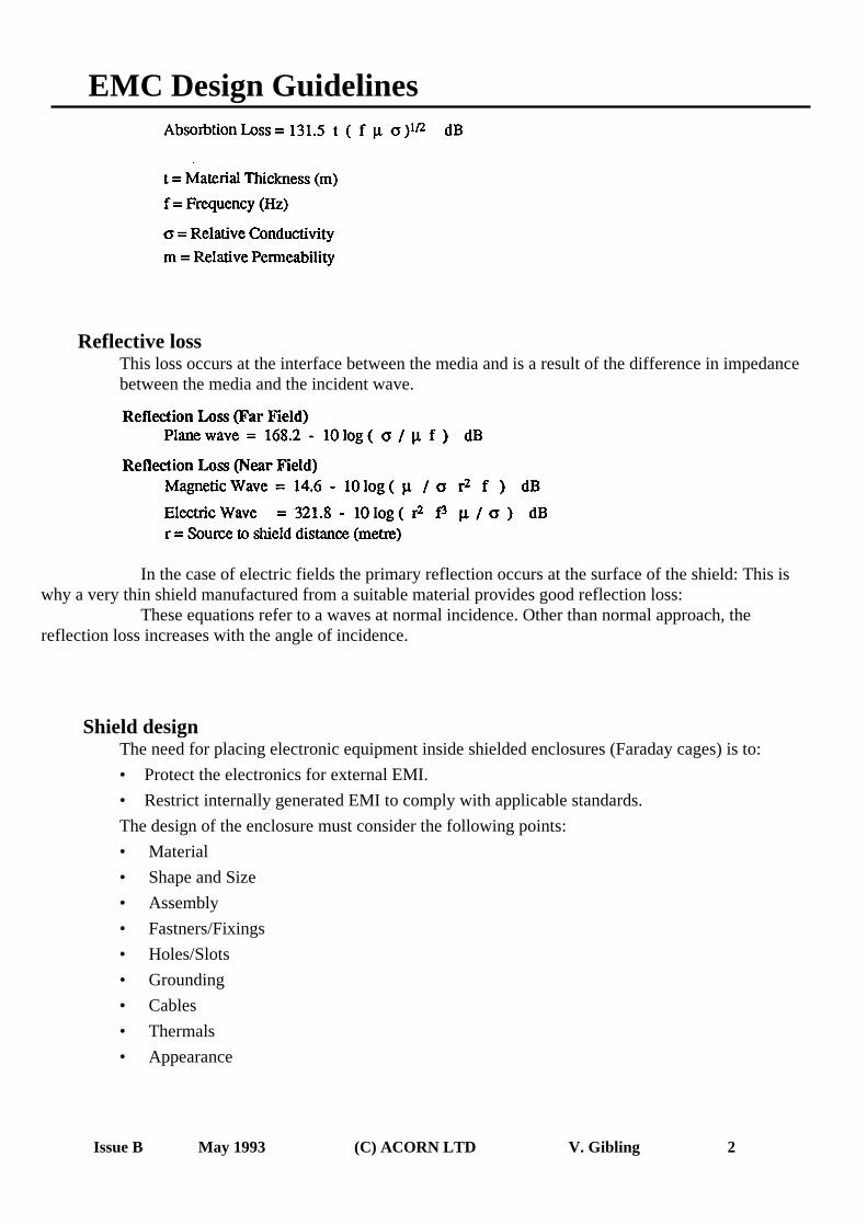
Absorption lossWhen an electromagnetic wave passes through a medium its amplitude decreases exponentially: This decay occurs because currents induced in the medium produce ohmic losses and heating: The reduction in field intensity is a feature of the material thickness, conductivity, permeability, and the frequency of interest.
Issue B May 1993 (C) ACORN LTD V. Gibling 1
EMC Design Guidelines
Reflective lossThis loss occurs at the interface between the media and is a result of the difference in impedance between the media and the incident wave.
In the case of electric fields the primary reflection occurs at the surface of the shield: This is why a very thin shield manufactured from a suitable material provides good reflection loss:
These equations refer to a waves at normal incidence. Other than normal approach, the reflection loss increases with the angle of incidence.
Shield designThe need for placing electronic equipment inside shielded enclosures (Faraday cages) is to:
• Protect the electronics for external EMI.
• Restrict internally generated EMI to comply with applicable standards.
The design of the enclosure must consider the following points:
• Material
• Shape and Size
• Assembly
• Fastners/Fixings
• Holes/Slots
• Grounding
• Cables
• Thermals
• Appearance
Issue B May 1993 (C) ACORN LTD V. Gibling 2
EMC Design Guidelines
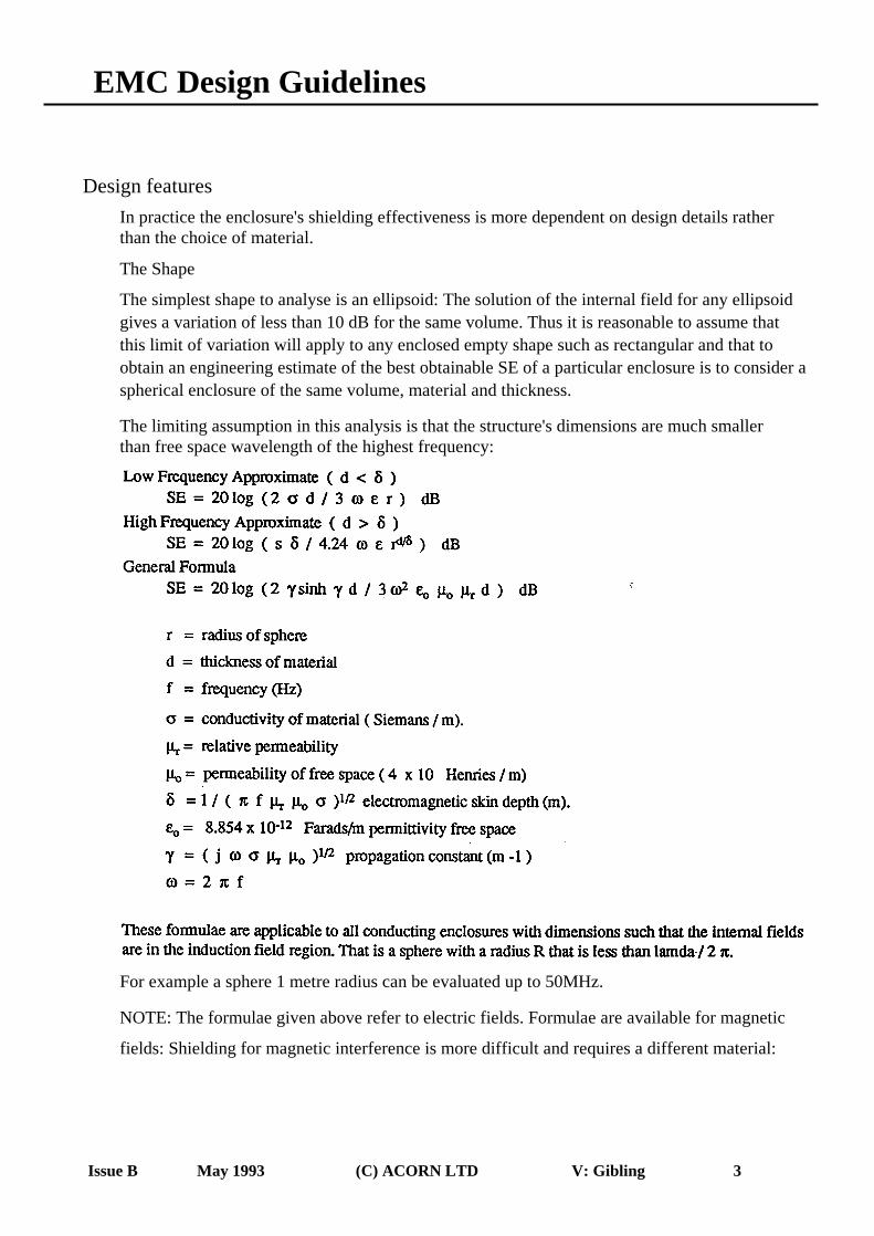
Design features
In practice the enclosure's shielding effectiveness is more dependent on design details rather than the choice of material.
The Shape
The simplest shape to analyse is an ellipsoid: The solution of the internal field for any ellipsoid gives a variation of less than 10 dB for the same volume. Thus it is reasonable to assume that this limit of variation will apply to any enclosed empty shape such as rectangular and that to obtain an engineering estimate of the best obtainable SE of a particular enclosure is to consider a spherical enclosure of the same volume, material and thickness.
The limiting assumption in this analysis is that the structure's dimensions are much smaller than free space wavelength of the highest frequency:
Electric Field Shielding Effectiveness Formulae.
For example a sphere 1 metre radius can be evaluated up to 50MHz.
NOTE: The formulae given above refer to electric fields. Formulae are available for magnetic
fields: Shielding for magnetic interference is more difficult and requires a different material:
Issue B May 1993 (C) ACORN LTD V: Gibling 3
EMC Design Guidelines
Enclosure designSeams, interfaces, holes and slotsThe design of interfaces should be to ensure a uniform low impedance join: The number of fixing points will determine its uniformity. To visualise this consider the induced currents flowing: For these currents to generate the additional field which will cancel the original field they must flow undisturbed in the manner in which they are induced. If a discontinuity forces the current to flow in a different path, the shielding effictiveness is reduced. The further the detour the greater this decrease will be: Holes and slots should be considered similarly.
If the join only makes contact at intervals then the total resistance is likely to be much higher than a well fitting join, resulting in a reduction in shielding integrity:
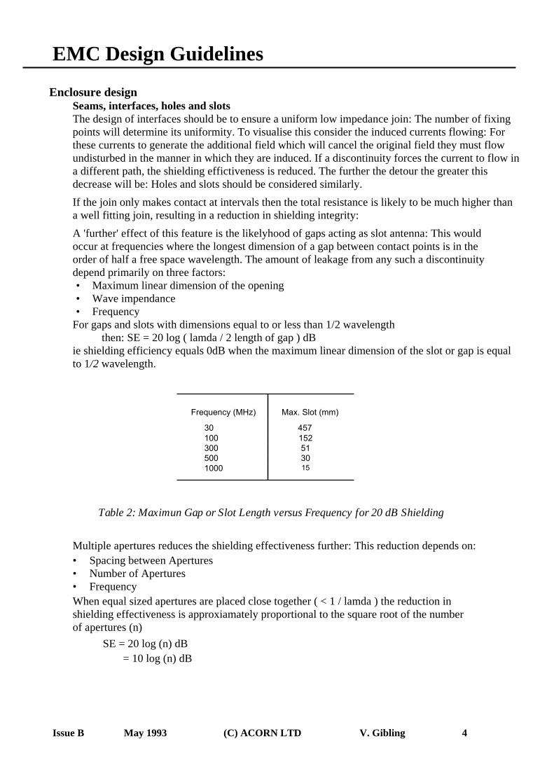
A 'further' effect of this feature is the likelyhood of gaps acting as slot antenna: This would occur at frequencies where the longest dimension of a gap between contact points is in the order of half a free space wavelength. The amount of leakage from any such a discontinuity depend primarily on three factors:• Maximum linear dimension of the opening• Wave impendance• Frequency
For gaps and slots with dimensions equal to or less than 1/2 wavelengththen: SE = 20 log ( lamda / 2 length of gap ) dB
ie shielding efficiency equals 0dB when the maximum linear dimension of the slot or gap is equal to 1/2 wavelength.
Frequency (MHz) Max. Slot (mm)
30 457100 152300 51500 301000 15
Table 2: Maximun Gap or Slot Length versus Frequency for 20 dB Shielding
Multiple apertures reduces the shielding effectiveness further: This reduction depends on:• Spacing between Apertures• Number of Apertures• FrequencyWhen equal sized apertures are placed close together ( < 1 / lamda ) the reduction in shielding effectiveness is approxiamately proportional to the square root of the number of apertures (n)
SE = 20 log (n) dB= 10 log (n) dB
Issue B May 1993 (C) ACORN LTD V. Gibling 4
EMC Design GuidelinesA similar approach can be taken for arrays of holes. For an array of equally spaced holes then:
SE ( k t) / g + 20 log ( C2 / D) dB
k = 27 for square holes
32 for circular holes
t = Material thickness
g = width of square holes or diameter of circular holes
C = Centre to centre spacing of holes
D = Length of aperture for square or diameter for circular aperture
If the holes are not equally spaced then C2 is replaced by A / N
Where A = Area of Aperture (D )
N = Number of holes
To achieve the best shielding effectiveness from arrays of holes or slots a suggested approach is to ensure that any dimension is not a multiple of any other: To achieve this a prime number can be applied, ie if any series of numbers are prime number multiples of a common base then no number in the series will be a multiple of any other: For example if the vent area is to be 280 square millimetres then a set of 7 slots in 3 groups, each slot 37mm x 11mm with the slots spaced at 7mm and 13mm between groups will give no resonances under 800MHz:
If the maximum frequency of interest is unknown then work on the basis that it is equal to the reciprocal of Pi times the typical rise time of the logic families used or the fifth harmonic of the fastest clock what ever is the greatest. eg: If the maximum clock frequency is say 96MHz then this corresponds to a maximum slot length of 62 mm: However if this dimension is significant with respect to the overall dimensions of the enclosure than this it should be reduced.
Holes are prefered to slots.
BondingThe overall design of the enclosure should consider the employment of a Star Ground: This is a point or plane to which all grounding routes are brought and from which the safety earth is taken. In general this point is best located close to where the safety earth enters the enclosure and ideally should be close to the panel to which the connectors are bonded. Consistant with this concept is an enclosure design in which the lower wrap included the connector panel through which the mains entered.
Ensure continuous electrical contact between all metal fittings and chassis: The design of any bonding or joint should be to give a very low impedance connection particularly at high frequencies: Bonding arrangements of less than 10 milliohms can be achieved: If a non-conductive surface is present over a conductive surface then a piercing star washer is required:
To assist a low impedance joint between mating parts an overlap should be employed however care is needed in its implimentation (see Seams, interfaces, holes and slots):
Edge effectsEnergy absorbed by the shield is channeled through the shield to edges where secondary interference can occur. For example, conductive fasteners penetrating the shield can act as small pole antenna and radiate secondary fields.
It can also occur at overlaps, these can be eliminated by folding seams back so that all edges are outside the enclosure.
Issue B May 1993 (C) ACORN LTD V. Gibling 5
EMC Design Guidelines
Cables and ConnectorsAny cable shielding should terminate at the enclosure. Attention must be paid to the connectors fixing: It is important for the connector body to be bonded to the panel to which they attatch via low impedance fixings. The panel itself must also be similarly bonded to the main enclosure ground (star point): lithe panel has a non conductive finish over the conductive material then paint piercing washers or selective exposed areas must be considered.
Internal Standing WavesEnergy enclosed in a metal box will bounce of the walls. The lowest resonant frequency of such an enclosure is given by:
resonant frequency (MHz) = 212 / largest dimension (metre)
Plastic enclosuresWhen designing a plastic enclosure the following extra points should be considered:• The choice of plating process. Not all plating processes are compatible with all
plastics and some processess deteriorate under humid conditions.
• If selective plating or a post plating process is to be used ensure the enclosure design will allow for cost effective masking:
• Connectivity between mating parts is best accomplished with flexible fingers: These should give a wiping action on assembly and accomodate design tolerances: The spacing of the fingers should be consistant with the rule for maximum slot length and hole/slot arrangements:
• All internal corners should be rounded with least at 1mm radius. This is particularly important for earth fixing bosses.
• Opposite screw bosses should not make contact with each other.• Provide a counterbore to all holes where thread forming screws are used:• Design without undercuts or narrow channels to ensure consistancy of plating:
Metal enclosuresWhen designing a metal enclosure the following extra points should be considered:• The choice of metal used as not ALL metals are suitable. Consideration must be
given to many other design requirements. In general any solid shield thick enough to be practical provides more than adequate shielding for most applications. It is the discontinuities such as slots and interfaces that determine the practical level of shielding effectiveness:
• Where non conductive coatings are applied to a conductive suface then star washers should be used. A paint-free or clean area is prefered.
• Connectivity between mating parts is best accomplished with flexible fingers: These• should give a wiping action on assembly and accomodate design tolerances: The
spacing of the fingers should be consistant with the rule for maximum slot length and hole/slot arrangements.
Issue B May 1993 (C) ACORN LTD V. Gibling 6
EMC Design Guidelines
Summary of shielded enclosure design considerations.
• Selection of material - Type of EM wave electric, magnetic or plane- Reflection loss is large for electric fields and plane waves- Reflection loss is normally small for low frequency magnetic
fields:- Magnetic fields are harder to shield than electric:- Use a good conductor to shield against electric fields, plane waves
and high frequency magnetic fields:- Above 10 MHz, the absorption loss predominates, and any solid
shield thick enough to be practical provides more than adequate shielding for most applications:
- Environmental requirements:- Level of attenuation:
• Joins and seams - Ease of assembly and maintainability:- Ensure low impedance joints between mating parts: An interference
fit is probably not good enough.
- Use lap joins where possible:
• Size of Holes/Slots - Thermal consideration:- SE decreases with the square root of the number of apertures
and directly with the maximum linear dimension of the aperture:
- Actual SE obtained in practice is usually determined by the leakages at joins and seams, not by the the SE of the material:
- The maximum dimension (not area) of a hole or discontinuity determines the amount of leakage: This should not exceed one tenth the wavelength of the maximum frequency of interest.
- Holes are prefered to slots:- Array holes and slots into irregular patterns:
• Connector Tennination - Ensure low impedance bond between connector body and mounting plate or panel:
• Star/Main Ground point - Close to point of entry of safety earth.- Close to Connectors:
• Edge Effect - Slots- Holes- Overlaps- Protrusions
Issue B May 1993 (C) ACORN LTD V. Gibling 7
EMC design guidelines for PCB layout
IntroductionThe speed and complexity of computers results in the generation of electromagnetic emissions which must be controlled to within the limits dictated by various national and international standards: This control can be achieved by applying EMC techniques to the complete system design. It must be stressed that the same degree of attention must be applied to all aspects of the system including the peripherals.
The layout of the pcb is particularly important as it is a major source of emissions and is therefore the place to start containing them at a low level. At best a correctly designed pcb will result in minimal reliance on other EMC measures but such achievements will not be attained easily or cheaply though success will have the advantage of keeping the overall EMC cost to a minimum:
The object of this section is to present some of the mechanisms which generate emissions on a pcb and some suggestions as to their control: Firstly it is important to appreciate that the final board layout cannot be left to one man, the pcb designer: It is necessary for several persons, usually with conflicting requirements, to be involved in achieving a satisfactory manufacturable board. Those involved alongside the pcb engineer must include the circuit's design engineer whose intimate knowledge of the circuit will enable specific areas and interactions to be highlighted: It is he/she who is expected to understand the electrical parameters affecting the working of the circuit and must make the necessary allowances for them. This is most important with respect to high speed logic circuits in which component and track lengths become very important, sometimes critical. This later point will be felt more when using CAD systems whose auto routing may well have to be manually circumvented. The pcb design may be further complicated by the need to subdivide the pcb into specific zones sometimes with individual power and grounding arrangements which may require tracking into/out of these areas only at specific points.
From a production viewpoint the requirements of EMC and high speed logic design will often be at variance with their wishes. It may be difficult to ensure component placement is arranged for efficient assembly, ATE and inspection. For example it may be better to orientate an IC to take advantage of pinout topology rather than align all pin l's. Such apparent haphazard layout will also be seen by maintenance and service personnel as a disadvantage.
Because of the enormous variations possible in electronic design the following guide is intended to raise awareness of the areas where thought and consideration should be given: The coverage is not extensive and will concentrate on multilayer pcb's and digital design though many of the points raised will be applicable to other pcb and circuit types.
OverviewRadiation from digital electronics can occur as either differential mode or common mode radiation and it's energy increases with the operational bandwidth of the circuit.
Differential mode radiation results from high frequency ac current flowing around a loop which acts as a small antenna radiating magnetic fields. Such loops are inevitable and their
P C BFor most computer applications the multilayer board is the only feasible starting point as it offers the best base on which to build a 'clean' board.
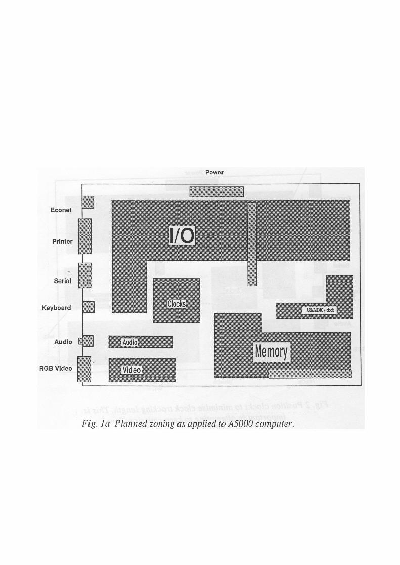
ZoningThis is the grouping together of activity associated circuitry related by function and/or operational speed or bandwidth: for example grouping I/O circuitry together, keeping high speed circuitry separate from low speed circuitry. These resulting zones should be contained in an area such that no track length exceeds the equivalent of one tenth its operational wavelength. Thus high speed circuitry should occupy a smaller area than slower speed circuitry.
Similarly sections of circuitry which may either generate high noise levels or are susceptible to noise can be contained within an island or a partially sectioned area of power and/or ground: These should be at the edge of the pcb to avoid destroying the integrity of the ground plane.
Example see Figures la and lb:
Track routing and component placementIt is good practice to organise the signal tracks close to their return, either the ground plane or a balanced return track. This has the effect of reducing the radiation or induced signal in the given field.
To minimise crosstalk high frequency clocks and signals should not run parallel to other tracks for long distances particularly sensitive I/O lines. Also track and signal impedances should be kept to a minimum to reduce noise pickup:
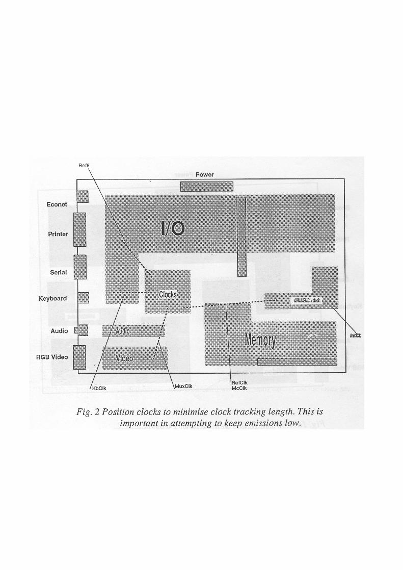
Clock lines which are a major source of noise should be as short as possible with NO tee's or spurs. Their layout should be considered early in conjunction with zoning and it is advisable to track them first. See figure 2.
Minimising crosstalk between adjacent signals can be achieved by interleaving a ground trace: The trace should have taps to ground every quarter wavelength of the signal's highest frequency component to ensure low impedance. The highest frequency component is related to the signal's rise time (tr) or fall time (tf), whichever is the fastest, by the following formula:
DecouplingDecoupling capacitors used with logic design provide the transient current demanded when the gates switch. Even with the advantage of a multilayer board and it's distributed capacitance it is necessary to provide local decoupling to minimise power supply noise.
These capacitors must provide high frequency currents and therefore should be a low inductance, high frequency type such as disc or multilayer ceramics. This inherent inductance is a consequence of their construction and along with the inductance of the circuit tracking they will self resonate. At frequencies below self resonance the capacitor behaves like a capacitor with it's impedance being a minimum at self resonance: Above these frequencies the capacitor acts as an inductor: This may necessitate using several capacitors with different values to account for high and low self resonance.
Most designers tend to use decoupling capacitors that are too large for the application and in general the smallest value that will do the job is best.
The optimum value of capacitor can only be found through a investigation on the finished pcb: This is achieved by measuring the dynamic noise waveform of the is and selecting a value to give an acceptable noise level: typically a value of 200mV for cmos and 100mV for TTL.
To provide adequate decoupling a minimum of one capacitor per two integrated circuit should be used though one per IC would be preferred: Some manufacturers give specific decoupling details for their devices and these should be sought particularly when dealing with the larger and more complex devices.
Decoupling capacitors should be placed close to the supply pin of the device it supports and if tracking is necessary it should be short and thick:
Component selectionThe operating current and frequency of the circuit will dictate the type of components selected but such choice should be decided with consideration to EMC: The lowest possible operating current and frequency consistent with the systems performance should be sought. The rise/fall times also impact on EMC performance, in general the faster the logic speed the more difficult it is to control and the shorter the rise/fall times the broader the noise spectra.
Prepackaged clock oscillators must be selected with care: Many exhibit fast rise times and high fan out with RF levels varying by as much as 20dB for equivalent clocks from different manufacturers.