Embedded Dual-Band GSM Antenna Design - Vogel.de · Application Note | CST AG Embedded Dual-Band...
6
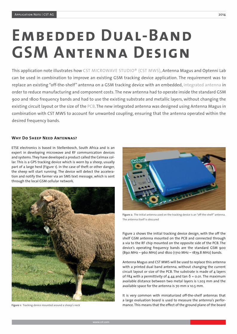
www.cst.com Application Note | CST AG 2014 Embedded Dual-Band GSM Antenna Design This application note illustrates how CST MICROWAVE STUDIO® (CST MWS) , Antenna Magus and Optenni Lab can be used in combination to improve an existing GSM tracking device application. The requirement was to replace an existing “off-the-shelf” antenna on a GSM tracking device with an embedded, integrated antenna in order to reduce manufacturing and component costs. The new antenna had to operate inside the standard GSM 900 and 1800 frequency bands and had to use the existing substrate and metallic layers, without changing the existing circuit layout or the size of the PCB. The new integrated antenna was designed using Antenna Magus in combination with CST MWS to account for unwanted coupling, ensuring that the antenna operated within the desired frequency bands. Why Do Sheep Need Antennas? ETSE electronics is based in Stellenbosch, South Africa and is an expert in developing microwave and RF communication devices and systems. They have developed a product called the Celmax col- lar. This is a GPS tracking device which is worn by a sheep, usually part of a large herd (Figure 1). In the case of theft or other danger, the sheep will start running. The device will detect the accelera- tion and notify the farmer via an SMS text message, which is sent through the local GSM cellular network. Figure 1: Tracking device mounted around a sheep’s neck Figure 2: The initial antenna used on the tracking device is an “off-the-shelf” antenna. The antenna itself is obscured Figure 2 shows the initial tracking device design, with the off the shelf GSM antenna mounted on the PCB and connected through a via to the RF chip mounted on the opposite side of the PCB. The device’s operating frequency bands are the standard GSM 900 (890 MHz – 960 MHz) and 1800 (1710 MHz – 1879.8 MHz) bands. Antenna Magus and CST MWS will be used to replace this antenna with a printed dual band antenna, without changing the current circuit layout or size of the PCB. The substrate is made of 4 layers of FR4 with a permittivity of 4.44 and tan δ = 0.01. The maximum available distance between two metal layers is 1.203 mm and the available space for the antenna is 70 mm x 10.5 mm. It is very common with miniaturized off-the-shelf antennas that a large evaluation board is used to measure the antenna’s perfor- mance. This means that the effect of the ground plane of the board
Transcript of Embedded Dual-Band GSM Antenna Design - Vogel.de · Application Note | CST AG Embedded Dual-Band...
www.cst.com
Application Note | CST AG 2014
Embedded Dual-Band GSM Antenna Design This application note illustrates how CST MICROWAVE STUDIO® (CST MWS), Antenna Magus and Optenni Lab can be used in combination to improve an existing GSM tracking device application. The requirement was to replace an existing “off-the-shelf” antenna on a GSM tracking device with an embedded, integrated antenna in order to reduce manufacturing and component costs. The new antenna had to operate inside the standard GSM 900 and 1800 frequency bands and had to use the existing substrate and metallic layers, without changing the existing circuit layout or the size of the PCB. The new integrated antenna was designed using Antenna Magus in combination with CST MWS to account for unwanted coupling, ensuring that the antenna operated within the desired frequency bands.
Why Do Sheep Need Antennas?
ETSE electronics is based in Stellenbosch, South Africa and is an expert in developing microwave and RF communication devices and systems. They have developed a product called the Celmax col-lar. This is a GPS tracking device which is worn by a sheep, usually part of a large herd (Figure 1). In the case of theft or other danger, the sheep will start running. The device will detect the accelera-tion and notify the farmer via an SMS text message, which is sent through the local GSM cellular network.
Figure 1: Tracking device mounted around a sheep’s neck
Figure 2: The initial antenna used on the tracking device is an “off-the-shelf” antenna.
The antenna itself is obscured
Figure 2 shows the initial tracking device design, with the off the shelf GSM antenna mounted on the PCB and connected through a via to the RF chip mounted on the opposite side of the PCB. The device’s operating frequency bands are the standard GSM 900 (890 MHz – 960 MHz) and 1800 (1710 MHz – 1879.8 MHz) bands.
Antenna Magus and CST MWS will be used to replace this antenna with a printed dual band antenna, without changing the current circuit layout or size of the PCB. The substrate is made of 4 layers of FR4 with a permittivity of 4.44 and tan δ = 0.01. The maximum available distance between two metal layers is 1.203 mm and the available space for the antenna is 70 mm x 10.5 mm.
It is very common with miniaturized off-the-shelf antennas that a large evaluation board is used to measure the antenna’s perfor-mance. This means that the effect of the ground plane of the board
Application Note | CST AG Embedded Dual-Band GSM Antenna Design
www.cst.com
used during evaluation is often neglected. In reality, the whole structure (including the evaluation board) resonates and deter-mines the antenna’s reactive impedance. In practice most antennas are placed on modified, non-uniform substrates and are integrated with other components. This affects the characteristic impedance of the antenna which usually decreases efficiency and perfor-mance. There might be ways to compensate for these effects but that would require more information about the antenna in order to optimize the whole structure. Even with this information options are limited as the antenna is designed and packaged in isolation.
Advantages of Integrated Antenna Design
Integrating the antenna into the circuit design has several advan-tages compared to fitting a standard antenna package. Printing the antenna as part of the PCB has a lower costper-unit cost , since less assembly is required, and the the cost of “off-the-shelf” an-tenna component is also remonved, as the new printed antenna uses the existing PCB.
As mentioned previously, the engineer has no control over the an-tenna’s impedance or installed performance when using an exist-ing shelf component. When using an integrated design, one can more effectively compensate for effects like mismatch, losses and coupling between the antenna and the printed circuit. This will be demonstrated later in this article.
Another very important factor is the total antenna efficiency, which depends primarily on the impedance match between the antenna and the rest of the circuit, as well as losses in the substrate. By fol-lowing an integrated design approach, the engineer can simulate the complete design and compensate for any mismatch between the amplifier and printed antenna. A better match between the antenna and radio results in a much higher receive-to-transmit an-tenna range, and a more efficient antenna requires lower transmit power with less power reflected back into the amplifier. This will increase the life of the amplifier and battery.
Initial Design in Antenna Magus
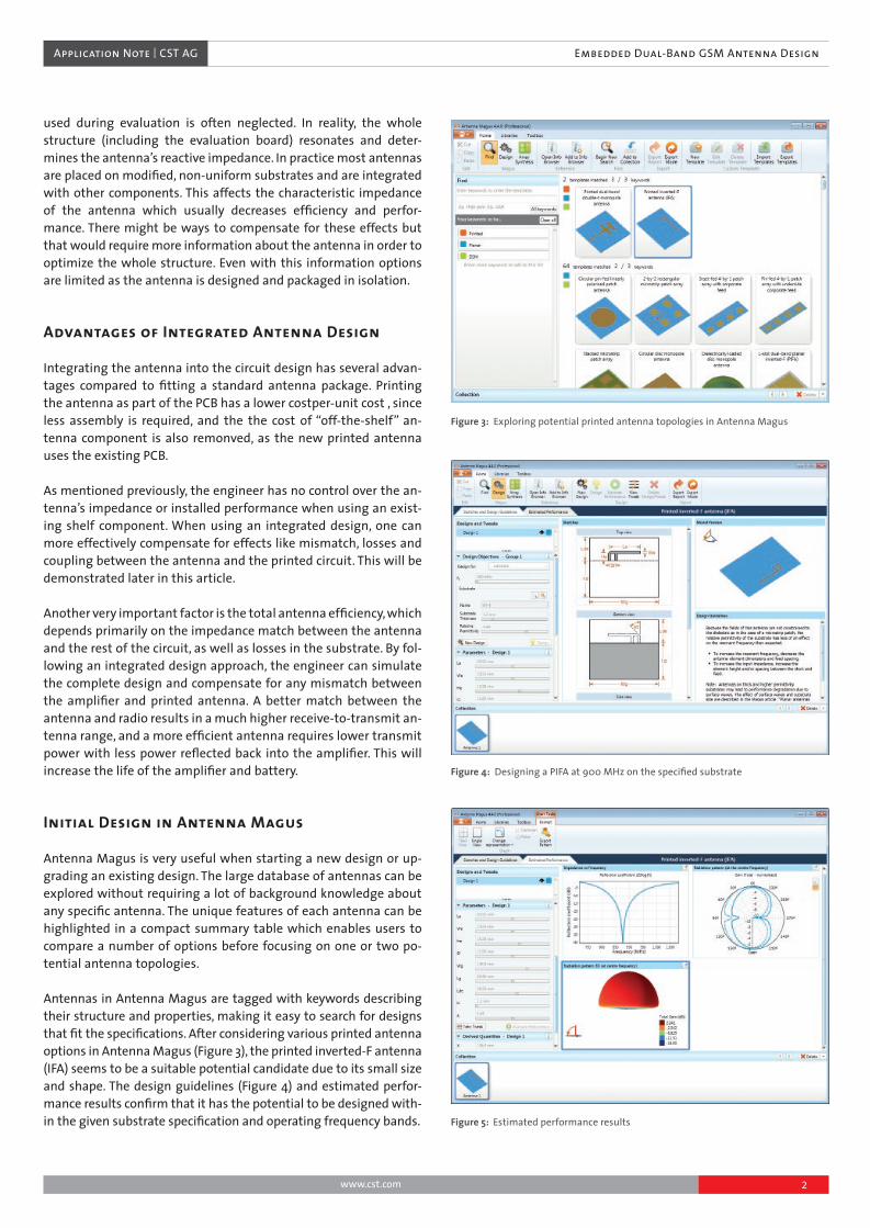
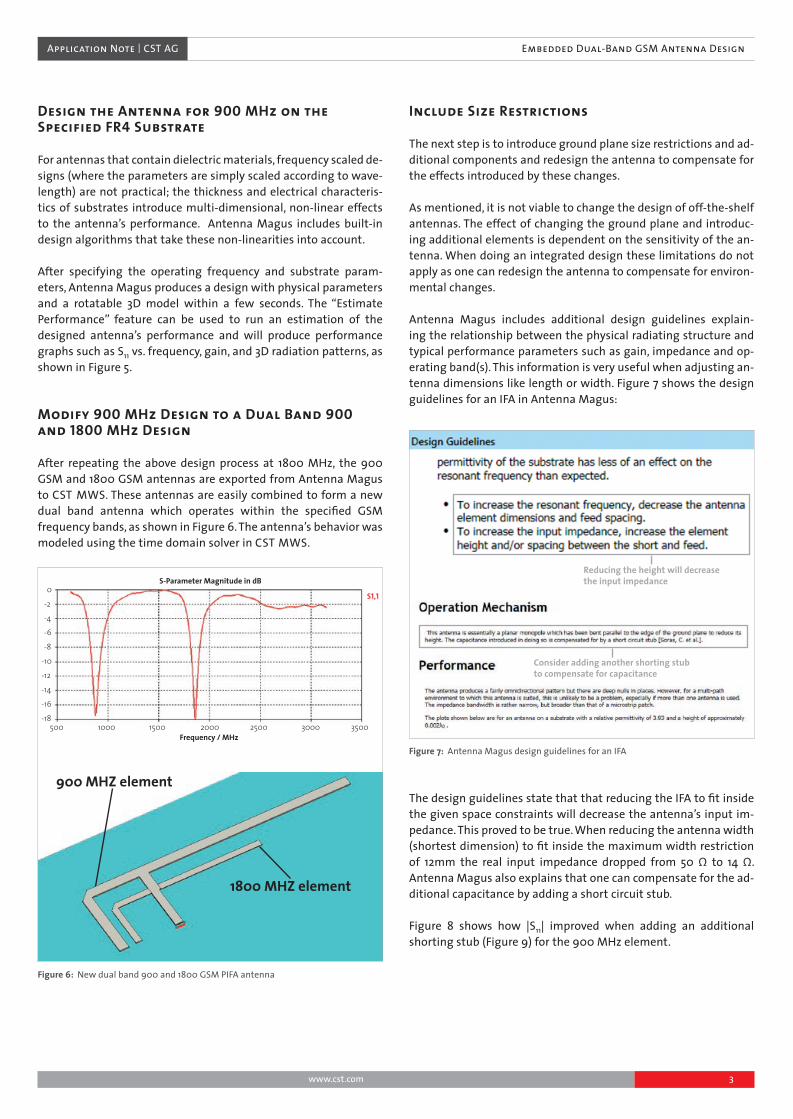
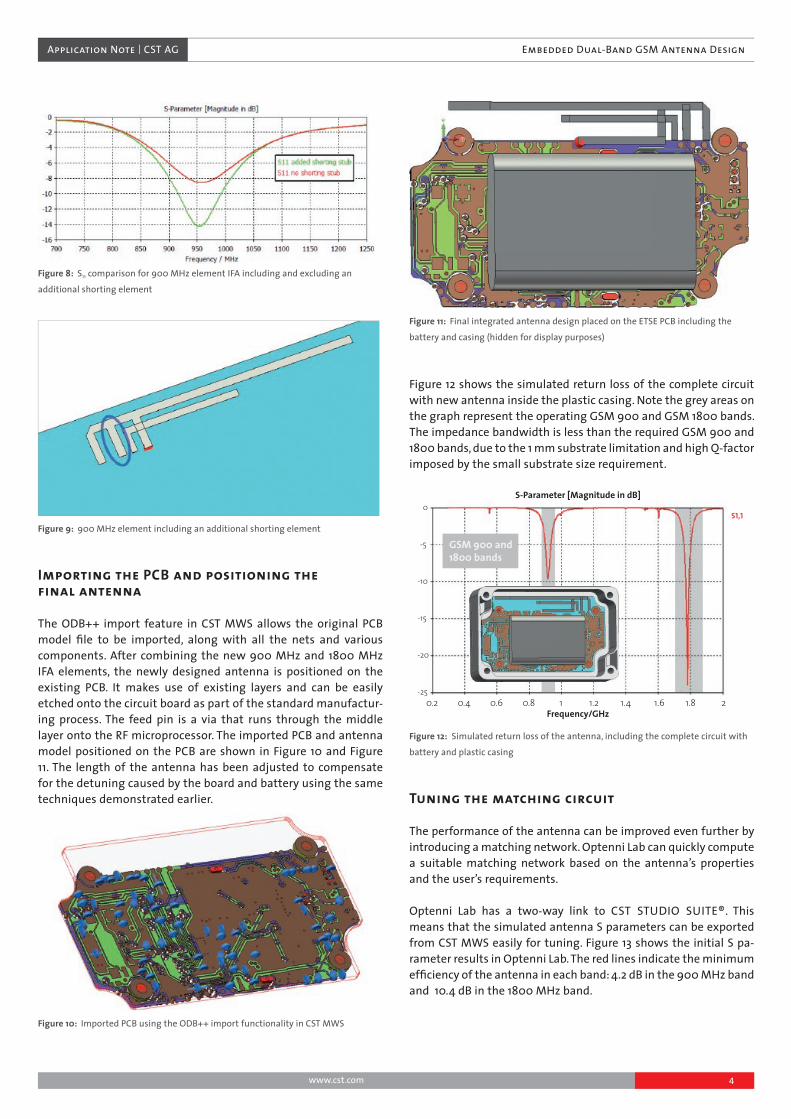
Antenna Magus is very useful when starting a new design or up-grading an existing design. The large database of antennas can be explored without requiring a lot of background knowledge about any specific antenna. The unique features of each antenna can be highlighted in a compact summary table which enables users to compare a number of options before focusing on one or two po-tential antenna topologies. Antennas in Antenna Magus are tagged with keywords describing their structure and properties, making it easy to search for designs that fit the specifications. After considering various printed antenna options in Antenna Magus (Figure 3), the printed inverted-F antenna (IFA) seems to be a suitable potential candidate due to its small size and shape. The design guidelines (Figure 4) and estimated perfor-mance results confirm that it has the potential to be designed with-in the given substrate specification and operating frequency bands.
Figure 3: Exploring potential printed antenna topologies in Antenna Magus
Figure 4: Designing a PIFA at 900 MHz on the specified substrate
Figure 5: Estimated performance results
2
Embedded Dual-Band GSM Antenna DesignApplication Note | CST AG
www.cst.com
Design the Antenna for 900 MHz on the Specified FR4 Substrate
For antennas that contain dielectric materials, frequency scaled de-signs (where the parameters are simply scaled according to wave-length) are not practical; the thickness and electrical characteris-tics of substrates introduce multi-dimensional, non-linear effects to the antenna’s performance. Antenna Magus includes built-in design algorithms that take these non-linearities into account.
After specifying the operating frequency and substrate param-eters, Antenna Magus produces a design with physical parameters and a rotatable 3D model within a few seconds. The “Estimate Performance” feature can be used to run an estimation of the designed antenna’s performance and will produce performance graphs such as S11 vs. frequency, gain, and 3D radiation patterns, as shown in Figure 5.
Modify 900 MHz Design to a Dual Band 900 and 1800 MHz Design
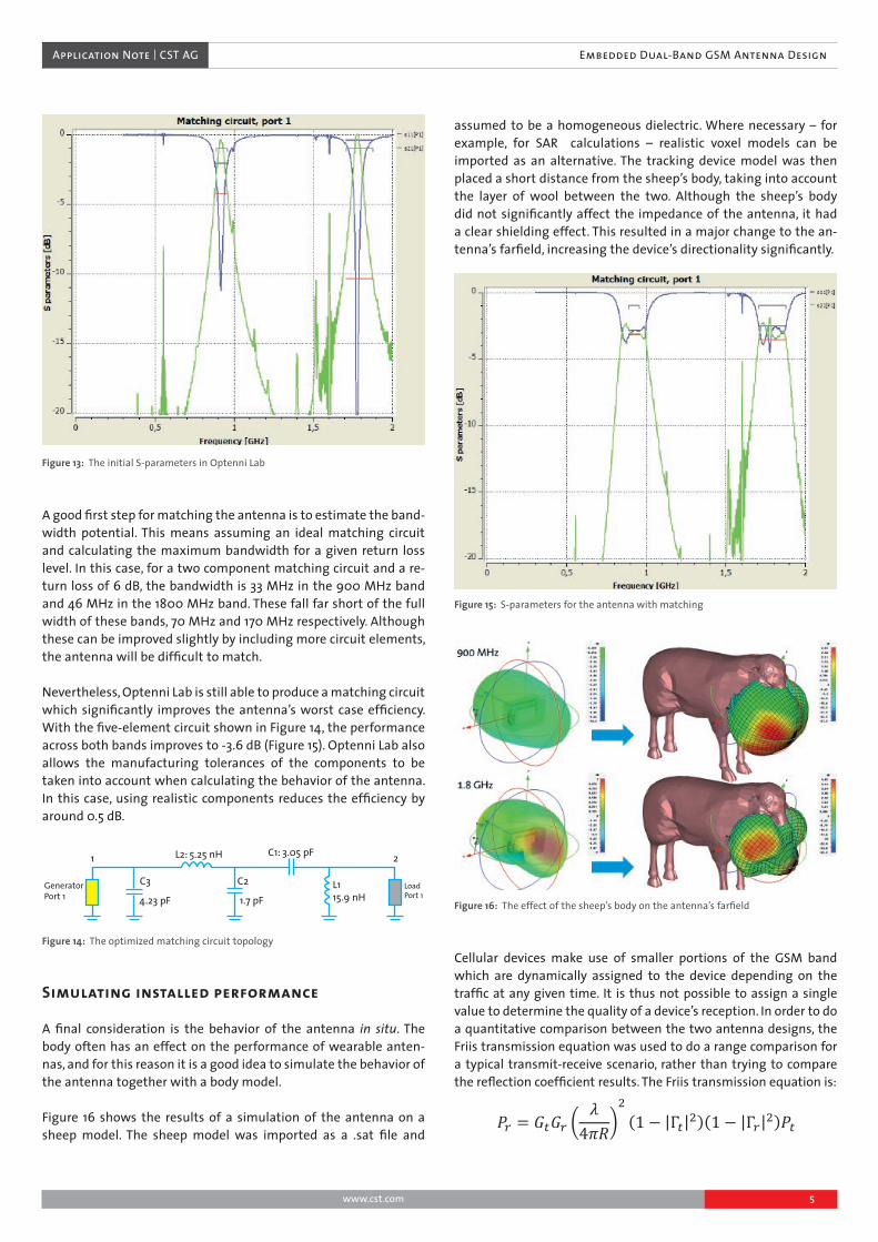
After repeating the above design process at 1800 MHz, the 900 GSM and 1800 GSM antennas are exported from Antenna Magus to CST MWS. These antennas are easily combined to form a new dual band antenna which operates within the specified GSM frequency bands, as shown in Figure 6. The antenna’s behavior was modeled using the time domain solver in CST MWS.
900 MHZ element
1800 MHZ element
Frequency / MHz
S-Parameter Magnitude in dB0
--2
--4
--6
--8
-10
-12
-14
-16
-18500 1000 1500 2000 2500 3000 3500
S1,1
Figure 6: New dual band 900 and 1800 GSM PIFA antenna
Include Size Restrictions
The next step is to introduce ground plane size restrictions and ad-ditional components and redesign the antenna to compensate for the effects introduced by these changes.
As mentioned, it is not viable to change the design of off-the-shelf antennas. The effect of changing the ground plane and introduc-ing additional elements is dependent on the sensitivity of the an-tenna. When doing an integrated design these limitations do not apply as one can redesign the antenna to compensate for environ-mental changes.
Antenna Magus includes additional design guidelines explain-ing the relationship between the physical radiating structure and typical performance parameters such as gain, impedance and op-erating band(s). This information is very useful when adjusting an-tenna dimensions like length or width. Figure 7 shows the design guidelines for an IFA in Antenna Magus:
Consider adding another shorting stub to compensate for capacitance
Reducing the height will decrease the input impedance
Figure 7: Antenna Magus design guidelines for an IFA
The design guidelines state that that reducing the IFA to fit inside the given space constraints will decrease the antenna’s input im-pedance. This proved to be true. When reducing the antenna width (shortest dimension) to fit inside the maximum width restriction of 12mm the real input impedance dropped from 50 Ω to 14 Ω. Antenna Magus also explains that one can compensate for the ad-ditional capacitance by adding a short circuit stub.
Figure 8 shows how |S11| improved when adding an additional shorting stub (Figure 9) for the 900 MHz element.
3
Application Note | CST AG Embedded Dual-Band GSM Antenna Design
www.cst.com
Figure 8: S11 comparison for 900 MHz element IFA including and excluding an
additional shorting element
Figure 9: 900 MHz element including an additional shorting element
Importing the PCB and positioning the final antenna
The ODB++ import feature in CST MWS allows the original PCB model fi le to be imported, along with all the nets and various components. After combining the new 900 MHz and 1800 MHz IFA elements, the newly designed antenna is positioned on the existing PCB. It makes use of existing layers and can be easily etched onto the circuit board as part of the standard manufactur-ing process. The feed pin is a via that runs through the middle layer onto the RF microprocessor. The imported PCB and antenna model positioned on the PCB are shown in Figure 10 and Figure 11. The length of the antenna has been adjusted to compensate for the detuning caused by the board and battery using the same techniques demonstrated earlier.
Figure 10: Imported PCB using the ODB++ import functionality in CST MWS
Figure 11: Final integrated antenna design placed on the ETSE PCB including the
battery and casing (hidden for display purposes)
Figure 12 shows the simulated return loss of the complete circuit with new antenna inside the plastic casing. Note the grey areas on the graph represent the operating GSM 900 and GSM 1800 bands. The impedance bandwidth is less than the required GSM 900 and 1800 bands, due to the 1 mm substrate limitation and high Q-factor imposed by the small substrate size requirement.
GSM 900 and 1800 bands
S-Parameter [Magnitude in dB]
Frequency/GHz
0
--5
-10
-15
-20
-250.2 0.4 0.6 0.8 1 1.2 1.4 1.6 1.8 2
S1,1
Figure 12: Simulated return loss of the antenna, including the complete circuit with
battery and plastic casing
Tuning the matching circuit
The performance of the antenna can be improved even further by introducing a matching network. Optenni Lab can quickly compute a suitable matching network based on the antenna’s properties and the user’s requirements.
Optenni Lab has a two-way link to CST STUDIO SUITE®. This means that the simulated antenna S parameters can be exported from CST MWS easily for tuning. Figure 13 shows the initial S pa-rameter results in Optenni Lab. The red lines indicate the minimum effi ciency of the antenna in each band: 4.2 dB in the 900 MHz band and 10.4 dB in the 1800 MHz band.
4
Application Note | CST AG Embedded Dual-Band GSM Antenna Design
www.cst.com
Figure 13: The initial S-parameters in Optenni Lab
A good first step for matching the antenna is to estimate the band-width potential. This means assuming an ideal matching circuit and calculating the maximum bandwidth for a given return loss level. In this case, for a two component matching circuit and a re-turn loss of 6 dB, the bandwidth is 33 MHz in the 900 MHz band and 46 MHz in the 1800 MHz band. These fall far short of the full width of these bands, 70 MHz and 170 MHz respectively. Although these can be improved slightly by including more circuit elements, the antenna will be difficult to match.
Nevertheless, Optenni Lab is still able to produce a matching circuit which significantly improves the antenna’s worst case efficiency. With the five-element circuit shown in Figure 14, the performance across both bands improves to -3.6 dB (Figure 15). Optenni Lab also allows the manufacturing tolerances of the components to be taken into account when calculating the behavior of the antenna. In this case, using realistic components reduces the efficiency by around 0.5 dB.
GeneratorPort 1
LoadPort 1
L2: 5.25 nH C1: 3.05 pF1 2
C3 C2 L115.9 nH4.23 pF 1.7 pF
Figure 14: The optimized matching circuit topology
Simulating installed performance
A final consideration is the behavior of the antenna in situ. The body often has an effect on the performance of wearable anten-nas, and for this reason it is a good idea to simulate the behavior of the antenna together with a body model.
Figure 16 shows the results of a simulation of the antenna on a sheep model. The sheep model was imported as a .sat file and
assumed to be a homogeneous dielectric. Where necessary – for example, for SAR calculations – realistic voxel models can be imported as an alternative. The tracking device model was then placed a short distance from the sheep’s body, taking into account the layer of wool between the two. Although the sheep’s body did not significantly affect the impedance of the antenna, it had a clear shielding effect. This resulted in a major change to the an-tenna’s farfield, increasing the device’s directionality significantly.
Figure 15: S-parameters for the antenna with matching
Figure 16: The effect of the sheep’s body on the antenna’s farfield
Cellular devices make use of smaller portions of the GSM band which are dynamically assigned to the device depending on the traffic at any given time. It is thus not possible to assign a single value to determine the quality of a device’s reception. In order to do a quantitative comparison between the two antenna designs, the Friis transmission equation was used to do a range comparison for a typical transmit-receive scenario, rather than trying to compare the reflection coefficient results. The Friis transmission equation is:
5
Embedded Dual-Band GSM Antenna DesignApplication Note | CST AG
www.cst.com
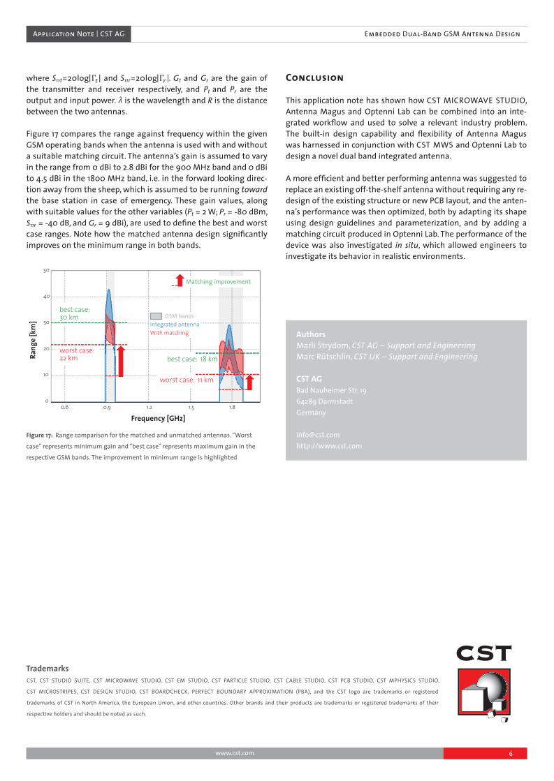
where S11t=20log and S11r=20log . Gt and Gr are the gain of the transmitter and receiver respectively, and Pt and Pr are the output and input power. is the wavelength and R is the distance between the two antennas.
Figure 17 compares the range against frequency within the given GSM operating bands when the antenna is used with and without a suitable matching circuit. The antenna’s gain is assumed to vary in the range from 0 dBi to 2.8 dBi for the 900 MHz band and 0 dBi to 4.5 dBi in the 1800 MHz band, i.e. in the forward looking direc-tion away from the sheep, which is assumed to be running toward the base station in case of emergency. These gain values, along with suitable values for the other variables (Pt = 2 W; Pr = -80 dBm, S11r = -40 dB, and Gr = 9 dBi), are used to define the best and worst case ranges. Note how the matched antenna design significantly improves on the minimum range in both bands.
Frequency [GHz]
Rang
e [k
m]
50
40
30
20
10
100.6 0.9 1.2 1.5 1.8
best case:30 km
Matching improvement
GSM bandsIntegrated antennaWith matching
worst case:22 km best case: 18 km
worst case: 11 km
Figure 17: Range comparison for the matched and unmatched antennas. “Worst
case” represents minimum gain and “best case” represents maximum gain in the
respective GSM bands. The improvement in minimum range is highlighted
Conclusion
This application note has shown how CST MICROWAVE STUDIO, Antenna Magus and Optenni Lab can be combined into an inte-grated workflow and used to solve a relevant industry problem. The built-in design capability and flexibility of Antenna Magus was harnessed in conjunction with CST MWS and Optenni Lab to design a novel dual band integrated antenna.
A more efficient and better performing antenna was suggested to replace an existing off-the-shelf antenna without requiring any re-design of the existing structure or new PCB layout, and the anten-na’s performance was then optimized, both by adapting its shape using design guidelines and parameterization, and by adding a matching circuit produced in Optenni Lab. The performance of the device was also investigated in situ, which allowed engineers to investigate its behavior in realistic environments.
AuthorsMarli Strydom, CST AG – Support and EngineeringMarc Rütschlin, CST UK – Support and Engineering
CST AGBad Nauheimer Str. 1964289 DarmstadtGermany
[email protected]://www.cst.com
6
Trademarks CST, CST STUDIO SUITE, CST MICROWAVE STUDIO, CST EM STUDIO, CST PARTICLE STUDIO, CST CABLE STUDIO, CST PCB STUDIO, CST MPHYSICS STUDIO,
CST MICROSTRIPES, CST DESIGN STUDIO, CST BOARDCHECK, PERFECT BOUNDARY APPROXIMATION (PBA), and the CST logo are trademarks or registered
trademarks of CST in North America, the European Union, and other countries. Other brands and their products are trademarks or registered trademarks of their
respective holders and should be noted as such.