EMB1428Q Switch Matrix Gate Driver datasheet … · EMB1428Q SNVS812A –MAY 2012–REVISED MAY...
31
EMB1428Q www.ti.com SNVS812A – MAY 2012 – REVISED MAY 2013 EMB1428Q Switch Matrix Gate Driver Check for Samples: EMB1428Q 1FEATURES DESCRIPTION The EMB1428 Switch Matrix Gate Driver IC is 2• 60V Maximum Stack Operating Voltage designed to work in conjunction with EMB1499 • Twelve (12) Floating Gate Drivers DC/DC Controller IC to support TI’s switch matrix • SPI Bus Interface (for Charge/discharge based active cell balancing scheme in a battery Commands and Fault Reporting) management system. The EMB1428 provides 12 floating MOSFET gate drivers necessary for • Low Power Sleep Mode balancing up to 7 battery cells connected in a series • EMB1428Q is an Automotive Grade Product stack. Multiple EMB1428 ICs may be used together that is AEC-Q100 Grade 1 Qualified (-40°C to to balance a stack of more than seven battery cells. +125°C Operating Junction Temperature) The EMB1428 integrated circuit interfaces with the EMB1499 DC/DC controller to control and enable APPLICATIONS charging and discharging modes. The EMB1428 uses • Li-Ion Battery Management Systems an SPI bus to accept commands from the main controller (CPU/MCU) on which battery cell should be • Electrical/Hybrid Vehicles charged or discharged and to report back any faults • Grid-Power Storage to the main controller (CPU/MCU). 1 Please be aware that an important notice concerning availability, standard warranty, and use in critical applications of Texas Instruments semiconductor products and disclaimers thereto appears at the end of this data sheet. 2All trademarks are the property of their respective owners. PRODUCTION DATA information is current as of publication date. Copyright © 2012–2013, Texas Instruments Incorporated Products conform to specifications per the terms of the Texas Instruments standard warranty. Production processing does not necessarily include testing of all parameters.
Transcript of EMB1428Q Switch Matrix Gate Driver datasheet … · EMB1428Q SNVS812A –MAY 2012–REVISED MAY...
EMB1428Q
www.ti.com SNVS812A –MAY 2012–REVISED MAY 2013
EMB1428Q Switch Matrix Gate DriverCheck for Samples: EMB1428Q
1FEATURES DESCRIPTIONThe EMB1428 Switch Matrix Gate Driver IC is
2• 60V Maximum Stack Operating Voltagedesigned to work in conjunction with EMB1499• Twelve (12) Floating Gate Drivers DC/DC Controller IC to support TI’s switch matrix
• SPI Bus Interface (for Charge/discharge based active cell balancing scheme in a batteryCommands and Fault Reporting) management system. The EMB1428 provides 12
floating MOSFET gate drivers necessary for• Low Power Sleep Modebalancing up to 7 battery cells connected in a series• EMB1428Q is an Automotive Grade Product stack. Multiple EMB1428 ICs may be used together
that is AEC-Q100 Grade 1 Qualified (-40°C to to balance a stack of more than seven battery cells.+125°C Operating Junction Temperature)
The EMB1428 integrated circuit interfaces with theEMB1499 DC/DC controller to control and enableAPPLICATIONS charging and discharging modes. The EMB1428 uses
• Li-Ion Battery Management Systems an SPI bus to accept commands from the maincontroller (CPU/MCU) on which battery cell should be• Electrical/Hybrid Vehiclescharged or discharged and to report back any faults• Grid-Power Storage to the main controller (CPU/MCU).
1
Please be aware that an important notice concerning availability, standard warranty, and use in critical applications ofTexas Instruments semiconductor products and disclaimers thereto appears at the end of this data sheet.
2All trademarks are the property of their respective owners.PRODUCTION DATA information is current as of publication date. Copyright © 2012–2013, Texas Instruments IncorporatedProducts conform to specifications per the terms of the TexasInstruments standard warranty. Production processing does notnecessarily include testing of all parameters.
FAULT2FAULT1FAULT0
GNDA GNDP
GNDP GND
CPU ORMCU
EMB1428
EMB1499
Vstack
SPI BUS
DAC
MOSFETDRIVER
DIR_RTDONE
DIR
+12V
GNDFPGNDF
PVINFFloating
12V Supply
GATE_HS2
VSENSE_HS
+3.3VVDD5V
VDDPVDD12V
VSTACK
CEXT1
CEXT2
VDDCP
GATE[11..0]
SOURCE[11..0]
+12V
+5V
FAULT0FAULT1FAULT2
DONEDIR_RT
DIREN
CSSD0SDI
SCLK
FAULT_INTRST
7-CellHalf-
Stack
Vstack
°
°¯
®
VINA
VDDIO
VINF
CELLPLUS
GATE_HS1
EN
VSET
VINP
VSENSE_LS
PWM_CLAMP
GATE_LS
TO OTHER BALANCING CIRCUIT
EMB1428Q
SNVS812A –MAY 2012–REVISED MAY 2013 www.ti.com
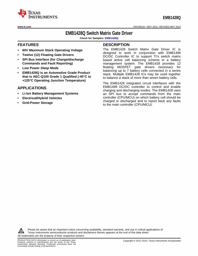
Typical Application
Figure 1. Typical Application
2 Submit Documentation Feedback Copyright © 2012–2013, Texas Instruments Incorporated
Product Folder Links: EMB1428Q
GNDP
VDDP
SOURCE7
GATE7
SOURCE6
GATE6
SOURCE5
GATE5
SOURCE4
GATE4
SOURCE3
GATE3
1
2
3
4
5
6
7
8
9
10
11
12
GND
RST
VDD12V
VDD5V
VDDIO
FAULT_INT
CS
SDO
SDI
SCLK
EN
DIR
36
35
34
33
32
31
30
29
28
27
26
25
48 47 46 45 44 43 42 41 40 39 38 37
VS
TA
CK
CE
XT
1
CE
XT
2
VD
DC
P
GA
TE
8
SO
UR
CE
8
4GA
TE
9
SO
UR
CE
9
GA
TE
10
SO
UR
CE
10
GA
TE
11
SO
UR
CE
11
13 14 15 16 17 18 19 20 21 22 23 24
GN
D
SO
UR
CE
2
GA
TE
2
SO
UR
CE
1
GA
TE
1
SO
UR
CE
0
GA
TE
0
FA
ULT
2
FA
ULT
1
FA
ULT
0
DO
NE
DIR
_RT
EMB1428(Top View)
* Exposed pad must be soldered to groundPlane to ensure rated performance
EMB1428Q
www.ti.com SNVS812A –MAY 2012–REVISED MAY 2013
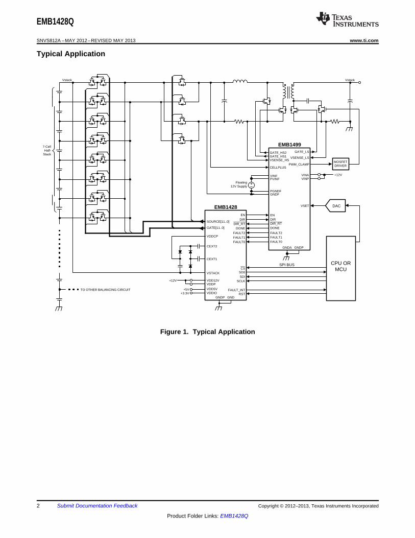
Connection Diagram
48-Pin WQFNSee RHS Package
Table 1. ORDERING INFORMATIONOrder number Package Package Supplied As Features
Type DrawingEMB1428QSQ 1000 Units in Tape and Reel AECQ100 Grade qualified. Automotive
EMB1428QSQE 250 Units in Tape andEMB1428QSQE WQFN RHS 250 Units in Tape and Reel Reel Grade Production Flow (1)
EMB1428QSQX 2500 Units in Tape and Reel
(1) Automotive Grade (Q) product incorporates enhanced manufacturing and support processes for the automotive market, including defectdetection methodologies. Reliability qualification is compliant with the requirements and temperature grades defined in the AEC-Q100standard. Automotive grade products are identified with the letter Q. For more information go to http://www.ti.com/automotive.
PIN DESCRIPTIONSPin Name Description Application Information1 GNDP Ground for charge pump circuitry Connect to stack ground at board level.2 VDDP 12V supply for charge pump circuitry Connect to 12V supply at board level with
0.1µF bypass cap to GNDP.3, 5, 7, 9, 11, 14, SOURCE0 to Floating driver references Connect to FET switch sources.16, 18, 37, 39, 41, SOURCE11
434, 6, 8, 10, 12, 15, GATE0 to GATE11 Floating driver outputs Connect to FET switch gates.17, 19, 38, 40, 42,
4413, 36 GND Ground Internal reference for all analog and digital
circuitry except the charge pump.20, 21, 22 FAULT[2, 1, 0] Inputs, three-bit digital fault code from Fault code is reported to CPU through the
EMB1499 SPI bus. 5V Schmitt-trigger inputs, 12Vsignal tolerant.
23 DONE Input from EMB1499, indicates end of charge 5V Schmitt-trigger input, 12V signal tolerant.cycle
Copyright © 2012–2013, Texas Instruments Incorporated Submit Documentation Feedback 3
Product Folder Links: EMB1428Q
EMB1428Q
SNVS812A –MAY 2012–REVISED MAY 2013 www.ti.com
PIN DESCRIPTIONS (continued)Pin Name Description Application Information24 DIR_RT Input from EMB1499, handshake signal, 5V Schmitt-trigger input, 12V signal tolerant.
inverted version of DIR25 DIR Output to EMB1499, indicates direction of 'High' indicates charge mode, 'Low' indicates
charging current discharge mode. 5V CMOS output levels.26 EN Output to EMB1499, enable signal for 'High' signals EMB1499 to begin charge or
charge/discharge cycle discharge cycle, 'Low' signals EMB1499 toramp down current and finish present cycle.5V CMOS levels.
27 SCLK SPI clock input 1MHz SPI interface, I/O levels arereferenced to the VDDIO supply.
28 SDI SPI data input29 SDO SPI data output30 CS SPI chip select input31 FAULT_INT Fault interrupt output to CPU Referenced to the VDDIO supply.32 VDDIO IO supply for SPI interface circuitry Connect to CPU supply to match I/O levels.33 VDD5V 5V supply for digital core and EMB1499
interface circuitry34 VDD12V 12V supply for analog core circuitry35 RST RESET pin45 VDDCP Floating supply input from external charge Connected to external charge pump circuit
pump circuit that provides a floating supply referenced tothe top of the battery module (VSTACK).
46, 47 CEXT1, CEXT2 Charge pump driver outputs Buffered, differential 1MHz clock signals fordriving external charge pump circuit.
48 VSTACK Supply from the highest voltage in the batterymodule
These devices have limited built-in ESD protection. The leads should be shorted together or the device placed in conductive foamduring storage or handling to prevent electrostatic damage to the MOS gates.
4 Submit Documentation Feedback Copyright © 2012–2013, Texas Instruments Incorporated
Product Folder Links: EMB1428Q
EMB1428Q
www.ti.com SNVS812A –MAY 2012–REVISED MAY 2013
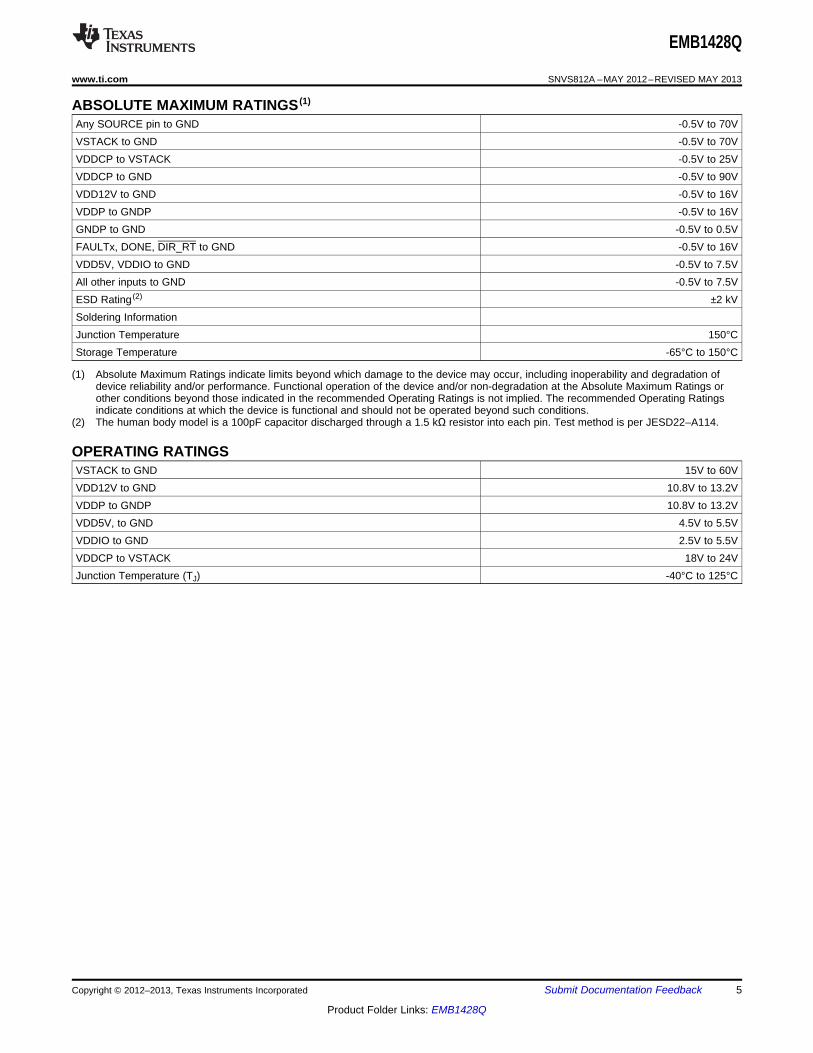
ABSOLUTE MAXIMUM RATINGS (1)
Any SOURCE pin to GND -0.5V to 70VVSTACK to GND -0.5V to 70VVDDCP to VSTACK -0.5V to 25VVDDCP to GND -0.5V to 90VVDD12V to GND -0.5V to 16VVDDP to GNDP -0.5V to 16VGNDP to GND -0.5V to 0.5VFAULTx, DONE, DIR_RT to GND -0.5V to 16VVDD5V, VDDIO to GND -0.5V to 7.5VAll other inputs to GND -0.5V to 7.5VESD Rating (2) ±2 kVSoldering InformationJunction Temperature 150°CStorage Temperature -65°C to 150°C
(1) Absolute Maximum Ratings indicate limits beyond which damage to the device may occur, including inoperability and degradation ofdevice reliability and/or performance. Functional operation of the device and/or non-degradation at the Absolute Maximum Ratings orother conditions beyond those indicated in the recommended Operating Ratings is not implied. The recommended Operating Ratingsindicate conditions at which the device is functional and should not be operated beyond such conditions.
(2) The human body model is a 100pF capacitor discharged through a 1.5 kΩ resistor into each pin. Test method is per JESD22–A114.
OPERATING RATINGSVSTACK to GND 15V to 60VVDD12V to GND 10.8V to 13.2VVDDP to GNDP 10.8V to 13.2VVDD5V, to GND 4.5V to 5.5VVDDIO to GND 2.5V to 5.5VVDDCP to VSTACK 18V to 24VJunction Temperature (TJ) -40°C to 125°C
Copyright © 2012–2013, Texas Instruments Incorporated Submit Documentation Feedback 5
Product Folder Links: EMB1428Q
EMB1428Q
SNVS812A –MAY 2012–REVISED MAY 2013 www.ti.com
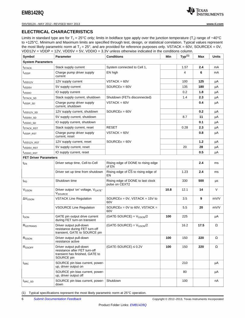
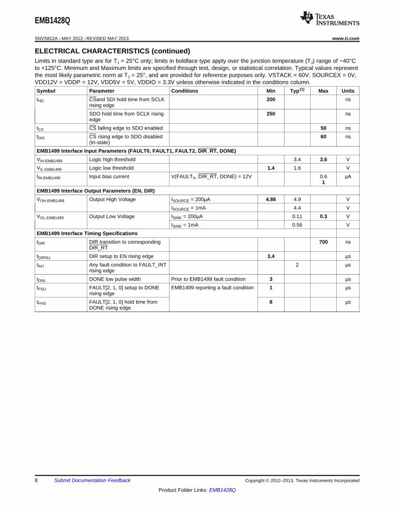
ELECTRICAL CHARACTERISTICSLimits in standard type are for TJ = 25°C only; limits in boldface type apply over the junction temperature (TJ) range of −40°Cto +125°C. Minimum and Maximum limits are specified through test, design, or statistical correlation. Typical values representthe most likely parametric norm at TJ = 25°, and are provided for reference purposes only. VSTACK = 60V, SOURCEX = 0V,VDD12V = VDDP = 12V, VDD5V = 5V, VDDIO = 3.3V unless otherwise indicated in the conditions column.Symbol Parameter Conditions Min Typ (1) Max UnitsSystem ParametersISTACK Stack supply current System connected to Cell 1, 1.57 2.4 mAIVDDP Charge pump driver supply EN high 4 6 mA
currentIVDD12V 12V supply current VSTACK = 60V 100 125 µAIVDD5V 5V supply current SOURCEx = 60V 135 180 µAIVDDIO IO supply current 0.2 1.8 µAISTACK_SD Stack supply current, shutdown Shutdown (FETs disconnected) 1.4 2.3 µAIVDDP_SD Charge pump driver supply VSTACK = 60V 0.4 µA
current, shutdownIVDD12V_SD 12V supply current, shutdown SOURCEx = 60V 0.2 µAIVDD5V_SD 5V supply current, shutdown 8.7 11 µAIVDDIO_SD IO supply current, shutdown 0.1 µAISTACK_RST Stack supply current, reset RESET 0.28 2.3 µAIVDDP_RST Charge pump driver supply VSTACK = 60V 0.8 µA
current, resetIVDD12V_RST 12V supply current, reset SOURCEx = 60V 1.2 µAIVDD5V_RST 5V supply current, reset 20 28 µAIVDDIO_RST IO supply current, reset 0.5 µAFET Driver ParameterstEN Driver setup time, Cell-to-Cell Rising edge of DONE to rising edge 2.4 ms
of ENDriver set up time from shutdown Rising edge of CS to rising edge of 1.23 2.4 ms
ENtPD Shutdown time Rising edge of DONE to last clock 330 500 µs
pulse on CEXT2VGSON Driver output 'on' voltage, VGATE- 10.8 12.1 14 V
VSOURCE
ΔVGSON VSTACK Line Regulation SOURCEx = 0V, VSTACK = 15V to 3.5 9 mV/V60V
VSOURCE Line Regulation SOURCEx = 0V to 60V, VSTACK = 5.5 20 mV/V60V
IGON GATE pin output drive current (GATE-SOURCE) = VGSON/2 100 225 µAduring FET turn-on transient
RGSTRANS Driver output pull-down (GATE-SOURCE) = VGSON/2 16.2 17.5 Ωresistance during FET turn-offtransient, GATE to SOURCE pin
RGSON Driver output pull-down 100 150 220 Ωresistance active
RGSOFF Driver output pull-down (GATE-SOURCE) ≤ 0.2V 100 150 220 Ωresistance after FET turn-offtransient has finished, GATE toSOURCE pin
ISRC SOURCE pin bias current, power- 210 µAup, driver output onSOURCE pin bias current, power- 80 µAup, driver output off
ISRC_SD SOURCE pin bias current, power- Shutdown 100 nAdown
(1) Typical specifications represent the most likely parametric norm at 25°C operation.
6 Submit Documentation Feedback Copyright © 2012–2013, Texas Instruments Incorporated
Product Folder Links: EMB1428Q
EMB1428Q
www.ti.com SNVS812A –MAY 2012–REVISED MAY 2013
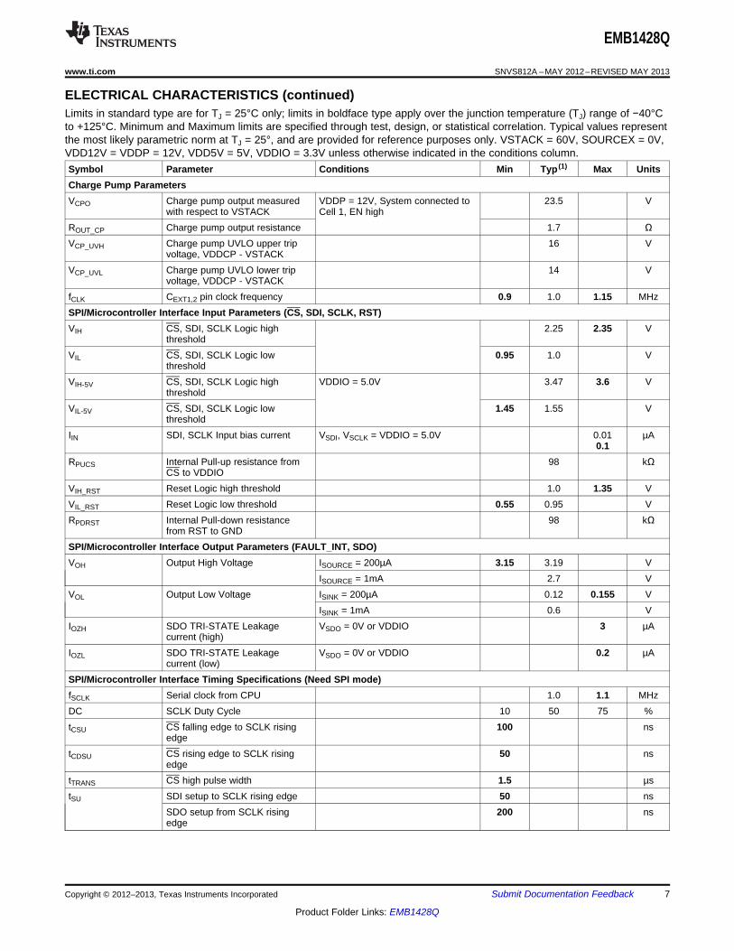
ELECTRICAL CHARACTERISTICS (continued)Limits in standard type are for TJ = 25°C only; limits in boldface type apply over the junction temperature (TJ) range of −40°Cto +125°C. Minimum and Maximum limits are specified through test, design, or statistical correlation. Typical values representthe most likely parametric norm at TJ = 25°, and are provided for reference purposes only. VSTACK = 60V, SOURCEX = 0V,VDD12V = VDDP = 12V, VDD5V = 5V, VDDIO = 3.3V unless otherwise indicated in the conditions column.Symbol Parameter Conditions Min Typ (1) Max UnitsCharge Pump ParametersVCPO Charge pump output measured VDDP = 12V, System connected to 23.5 V
with respect to VSTACK Cell 1, EN highROUT_CP Charge pump output resistance 1.7 ΩVCP_UVH Charge pump UVLO upper trip 16 V
voltage, VDDCP - VSTACKVCP_UVL Charge pump UVLO lower trip 14 V
voltage, VDDCP - VSTACKfCLK CEXT1,2 pin clock frequency 0.9 1.0 1.15 MHzSPI/Microcontroller Interface Input Parameters (CS, SDI, SCLK, RST)VIH CS, SDI, SCLK Logic high 2.25 2.35 V
thresholdVIL CS, SDI, SCLK Logic low 0.95 1.0 V
thresholdVIH-5V CS, SDI, SCLK Logic high VDDIO = 5.0V 3.47 3.6 V
thresholdVIL-5V CS, SDI, SCLK Logic low 1.45 1.55 V
thresholdIIN SDI, SCLK Input bias current VSDI, VSCLK = VDDIO = 5.0V 0.01 µA
0.1RPUCS Internal Pull-up resistance from 98 kΩ
CS to VDDIOVIH_RST Reset Logic high threshold 1.0 1.35 VVIL_RST Reset Logic low threshold 0.55 0.95 VRPDRST Internal Pull-down resistance 98 kΩ
from RST to GNDSPI/Microcontroller Interface Output Parameters (FAULT_INT, SDO)VOH Output High Voltage ISOURCE = 200µA 3.15 3.19 V
ISOURCE = 1mA 2.7 VVOL Output Low Voltage ISINK = 200µA 0.12 0.155 V
ISINK = 1mA 0.6 VIOZH SDO TRI-STATE Leakage VSDO = 0V or VDDIO 3 µA
current (high)IOZL SDO TRI-STATE Leakage VSDO = 0V or VDDIO 0.2 µA
current (low)SPI/Microcontroller Interface Timing Specifications (Need SPI mode)fSCLK Serial clock from CPU 1.0 1.1 MHzDC SCLK Duty Cycle 10 50 75 %tCSU CS falling edge to SCLK rising 100 ns
edgetCDSU CS rising edge to SCLK rising 50 ns
edgetTRANS CS high pulse width 1.5 µstSU SDI setup to SCLK rising edge 50 ns
SDO setup from SCLK rising 200 nsedge
Copyright © 2012–2013, Texas Instruments Incorporated Submit Documentation Feedback 7
Product Folder Links: EMB1428Q
EMB1428Q
SNVS812A –MAY 2012–REVISED MAY 2013 www.ti.com
ELECTRICAL CHARACTERISTICS (continued)Limits in standard type are for TJ = 25°C only; limits in boldface type apply over the junction temperature (TJ) range of −40°Cto +125°C. Minimum and Maximum limits are specified through test, design, or statistical correlation. Typical values representthe most likely parametric norm at TJ = 25°, and are provided for reference purposes only. VSTACK = 60V, SOURCEX = 0V,VDD12V = VDDP = 12V, VDD5V = 5V, VDDIO = 3.3V unless otherwise indicated in the conditions column.Symbol Parameter Conditions Min Typ (1) Max UnitstHD CSand SDI hold time from SCLK 200 ns
rising edgeSDO hold time from SCLK rising 250 nsedge
tCS CS falling edge to SDO enabled 50 nstDIS CS rising edge to SDO disabled 60 ns
(tri-state)EMB1499 Interface Input Parameters (FAULT0, FAULT1, FAULT2, DIR_RT, DONE)VIH-EMB1499 Logic high threshold 3.4 3.6 VVIL-EMB1499 Logic low threshold 1.4 1.6 VIIN-EMB1499 Input bias current V(FAULTX, DIR_RT, DONE) = 12V 0.6 µA
1EMB1499 Interface Output Parameters (EN, DIR)VOH-EMB1499 Output High Voltage ISOURCE = 200µA 4.86 4.9 V
ISOURCE = 1mA 4.4 VVOL-EMB1499 Output Low Voltage ISINK = 200µA 0.11 0.3 V
ISINK = 1mA 0.56 VEMB1499 Interface Timing SpecificationstDIR DIR transition to corresponding 700 ns
DIR_RTtDIRSU DIR setup to EN rising edge 3.4 µstINT Any fault condition to FAULT_INT 2 µs
rising edgetDNL DONE low pulse width Prior to EMB1499 fault condition 3 µstFSU FAULT[2, 1, 0] setup to DONE EMB1499 reporting a fault condition 1 µs
rising edgetFHD FAULT[2, 1, 0] hold time from 8 µs
DONE rising edge
8 Submit Documentation Feedback Copyright © 2012–2013, Texas Instruments Incorporated
Product Folder Links: EMB1428Q
DRIVERLEVELSHIFT
SOFTSTART
DRVRUVLO
HV CURRENT MIRROR
SHUTDOWN BIAS100 nA
FLOATING DRIVER 12X
BANDGAP
VDDCPCEXT2
GATE
0.01P
0.01P
FROM TOP OF BATTERYSTACK (60V MAX)
CEXT1
SOURCE
VDDP
0.01P
EXTERNAL CIRCUITRY
DRIVER BIAS CURRENTGENERATOR
Approx. VSTACK + (2 X VDDP)
CHARGE PUMP
VDD5V
5V CORE LOGIC
GNDP
VDD5V
RST
VDDIO
CSCLKSDI
SDOFAULT_INT
MACHINEEMB1499INTER-FACE
5VI/O
1 MHzCLOCK
SPIINTER-FACE
STATE
bg_goodSWITCH _EN
SLEW
POR
CLKLEVEL SHIFT
VSTACK
bg_good
CHARGEPUMPUVLO
VDD12V
3.3VI/O
DIR_RTDONE
FAULT[2..0]DIREN
EMB1428Q
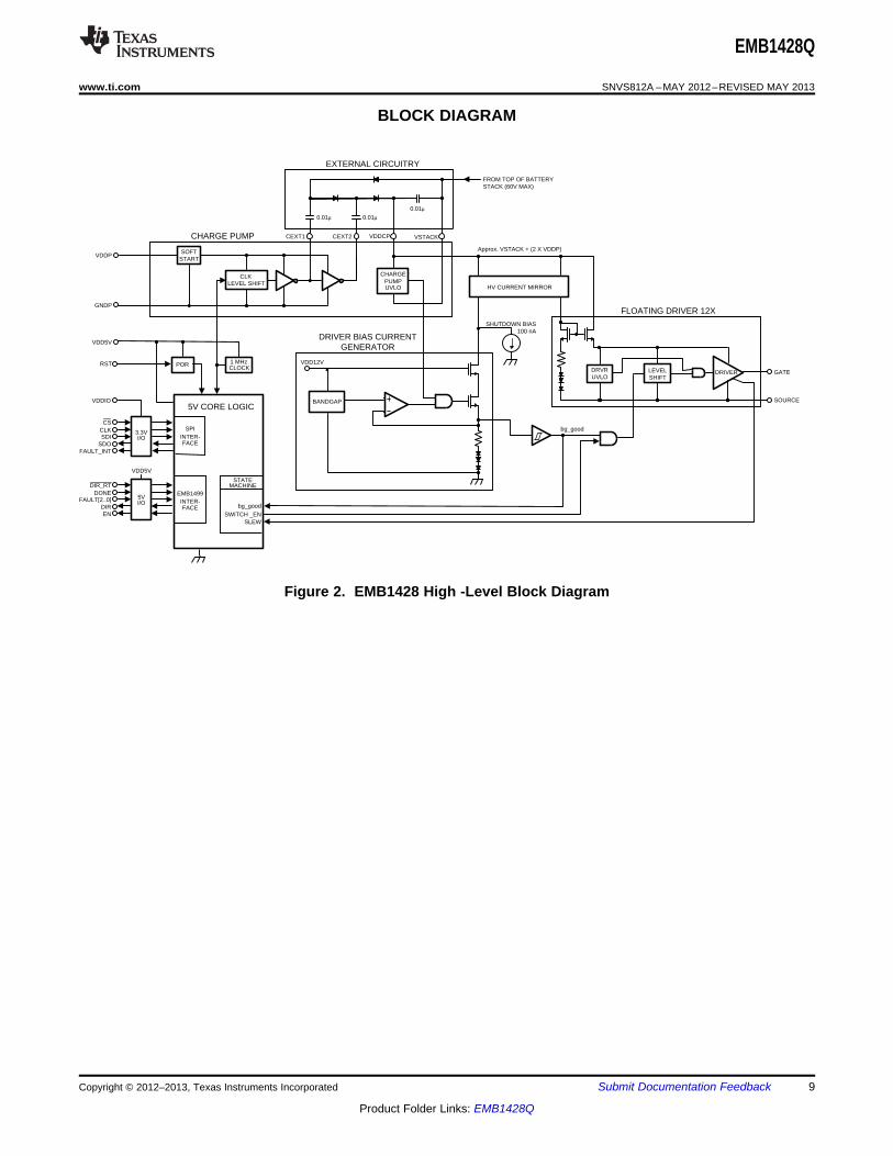
www.ti.com SNVS812A –MAY 2012–REVISED MAY 2013
BLOCK DIAGRAM
Figure 2. EMB1428 High -Level Block Diagram
Copyright © 2012–2013, Texas Instruments Incorporated Submit Documentation Feedback 9
Product Folder Links: EMB1428Q
EMB1428Q
SNVS812A –MAY 2012–REVISED MAY 2013 www.ti.com
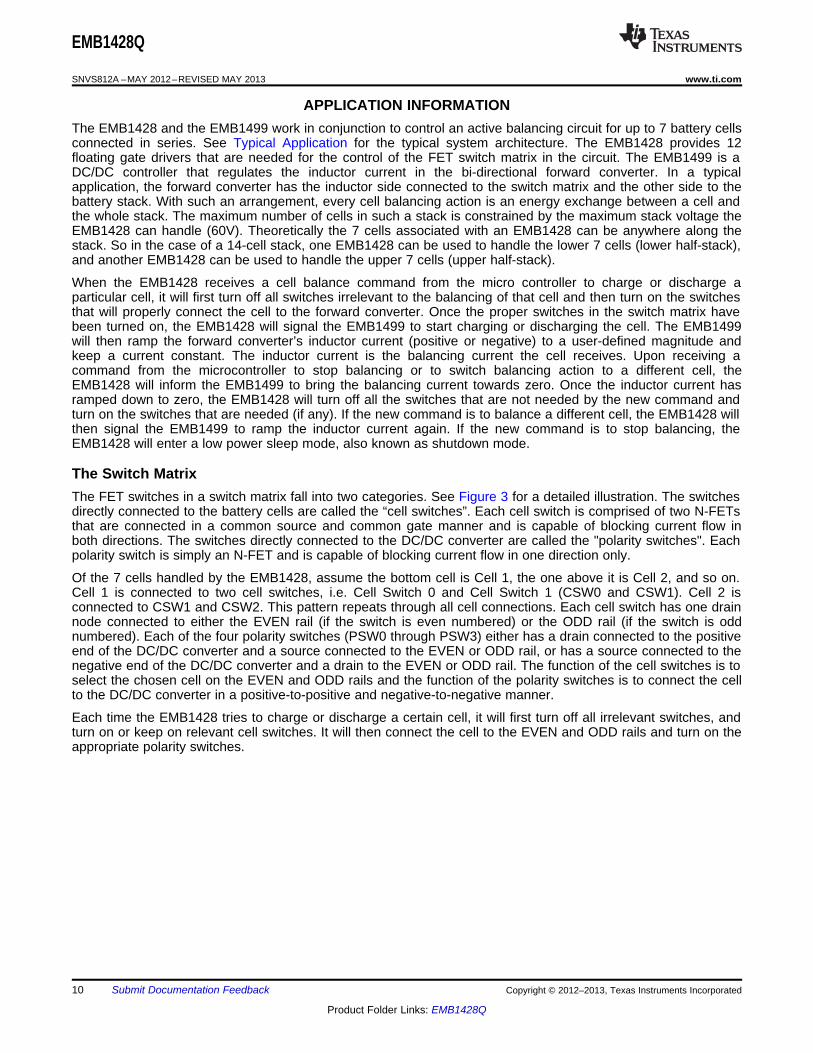
APPLICATION INFORMATIONThe EMB1428 and the EMB1499 work in conjunction to control an active balancing circuit for up to 7 battery cellsconnected in series. See Typical Application for the typical system architecture. The EMB1428 provides 12floating gate drivers that are needed for the control of the FET switch matrix in the circuit. The EMB1499 is aDC/DC controller that regulates the inductor current in the bi-directional forward converter. In a typicalapplication, the forward converter has the inductor side connected to the switch matrix and the other side to thebattery stack. With such an arrangement, every cell balancing action is an energy exchange between a cell andthe whole stack. The maximum number of cells in such a stack is constrained by the maximum stack voltage theEMB1428 can handle (60V). Theoretically the 7 cells associated with an EMB1428 can be anywhere along thestack. So in the case of a 14-cell stack, one EMB1428 can be used to handle the lower 7 cells (lower half-stack),and another EMB1428 can be used to handle the upper 7 cells (upper half-stack).
When the EMB1428 receives a cell balance command from the micro controller to charge or discharge aparticular cell, it will first turn off all switches irrelevant to the balancing of that cell and then turn on the switchesthat will properly connect the cell to the forward converter. Once the proper switches in the switch matrix havebeen turned on, the EMB1428 will signal the EMB1499 to start charging or discharging the cell. The EMB1499will then ramp the forward converter’s inductor current (positive or negative) to a user-defined magnitude andkeep a current constant. The inductor current is the balancing current the cell receives. Upon receiving acommand from the microcontroller to stop balancing or to switch balancing action to a different cell, theEMB1428 will inform the EMB1499 to bring the balancing current towards zero. Once the inductor current hasramped down to zero, the EMB1428 will turn off all the switches that are not needed by the new command andturn on the switches that are needed (if any). If the new command is to balance a different cell, the EMB1428 willthen signal the EMB1499 to ramp the inductor current again. If the new command is to stop balancing, theEMB1428 will enter a low power sleep mode, also known as shutdown mode.
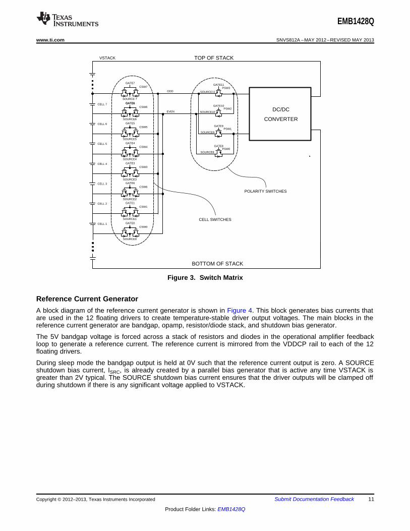
The Switch MatrixThe FET switches in a switch matrix fall into two categories. See Figure 3 for a detailed illustration. The switchesdirectly connected to the battery cells are called the “cell switches”. Each cell switch is comprised of two N-FETsthat are connected in a common source and common gate manner and is capable of blocking current flow inboth directions. The switches directly connected to the DC/DC converter are called the "polarity switches". Eachpolarity switch is simply an N-FET and is capable of blocking current flow in one direction only.
Of the 7 cells handled by the EMB1428, assume the bottom cell is Cell 1, the one above it is Cell 2, and so on.Cell 1 is connected to two cell switches, i.e. Cell Switch 0 and Cell Switch 1 (CSW0 and CSW1). Cell 2 isconnected to CSW1 and CSW2. This pattern repeats through all cell connections. Each cell switch has one drainnode connected to either the EVEN rail (if the switch is even numbered) or the ODD rail (if the switch is oddnumbered). Each of the four polarity switches (PSW0 through PSW3) either has a drain connected to the positiveend of the DC/DC converter and a source connected to the EVEN or ODD rail, or has a source connected to thenegative end of the DC/DC converter and a drain to the EVEN or ODD rail. The function of the cell switches is toselect the chosen cell on the EVEN and ODD rails and the function of the polarity switches is to connect the cellto the DC/DC converter in a positive-to-positive and negative-to-negative manner.
Each time the EMB1428 tries to charge or discharge a certain cell, it will first turn off all irrelevant switches, andturn on or keep on relevant cell switches. It will then connect the cell to the EVEN and ODD rails and turn on theappropriate polarity switches.
10 Submit Documentation Feedback Copyright © 2012–2013, Texas Instruments Incorporated
Product Folder Links: EMB1428Q
GATE6CSW6
EVEN
ODD
CELL 7
GATE5CSW5
CELL 6
GATE4CSW4
CELL 5
GATE3CSW3
CELL 4
GATE6CSW6
CELL 3
GATE1CSW1
CELL 2
GATE0CSW0
CELL 1
TOP OF STACK
DC/DC
CONVERTER
VSTACK
GATE6
GATE7CSW7
SOURCE 7
SOURCE6
SOURCE5
SOURCE1
SOURCE2
SOURCE0
SOURCE3
SOURCE4
PSW3GATE11
SOURCE11
PSW2GATE10
SOURCE10
PSW0GATE8
SOURCE8
PSW1GATE9
SOURCE9
BOTTOM OF STACK
CELL SWITCHES
POLARITY SWITCHES
EMB1428Q
www.ti.com SNVS812A –MAY 2012–REVISED MAY 2013
Figure 3. Switch Matrix
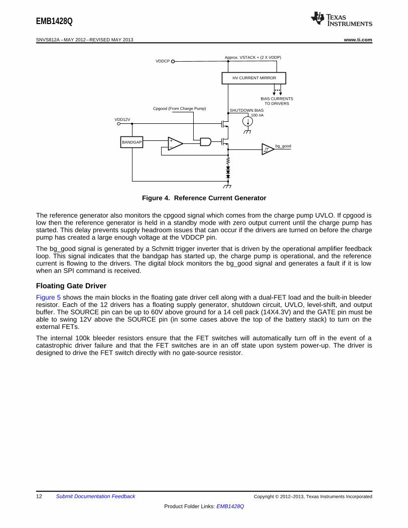
Reference Current GeneratorA block diagram of the reference current generator is shown in Figure 4. This block generates bias currents thatare used in the 12 floating drivers to create temperature-stable driver output voltages. The main blocks in thereference current generator are bandgap, opamp, resistor/diode stack, and shutdown bias generator.
The 5V bandgap voltage is forced across a stack of resistors and diodes in the operational amplifier feedbackloop to generate a reference current. The reference current is mirrored from the VDDCP rail to each of the 12floating drivers.
During sleep mode the bandgap output is held at 0V such that the reference current output is zero. A SOURCEshutdown bias current, ISRC, is already created by a parallel bias generator that is active any time VSTACK isgreater than 2V typical. The SOURCE shutdown bias current ensures that the driver outputs will be clamped offduring shutdown if there is any significant voltage applied to VSTACK.
Copyright © 2012–2013, Texas Instruments Incorporated Submit Documentation Feedback 11
Product Folder Links: EMB1428Q
SHUTDOWN BIAS100 nA
BANDGAP
Approx. VSTACK + (2 X VDDP)
bg_good
VDD12V
VDDCP
HV CURRENT MIRROR
Cpgood (From Charge Pump)
BIAS CURRENTSTO DRIVERS
EMB1428Q
SNVS812A –MAY 2012–REVISED MAY 2013 www.ti.com
Figure 4. Reference Current Generator
The reference generator also monitors the cpgood signal which comes from the charge pump UVLO. If cpgood islow then the reference generator is held in a standby mode with zero output current until the charge pump hasstarted. This delay prevents supply headroom issues that can occur if the drivers are turned on before the chargepump has created a large enough voltage at the VDDCP pin.
The bg_good signal is generated by a Schmitt trigger inverter that is driven by the operational amplifier feedbackloop. This signal indicates that the bandgap has started up, the charge pump is operational, and the referencecurrent is flowing to the drivers. The digital block monitors the bg_good signal and generates a fault if it is lowwhen an SPI command is received.
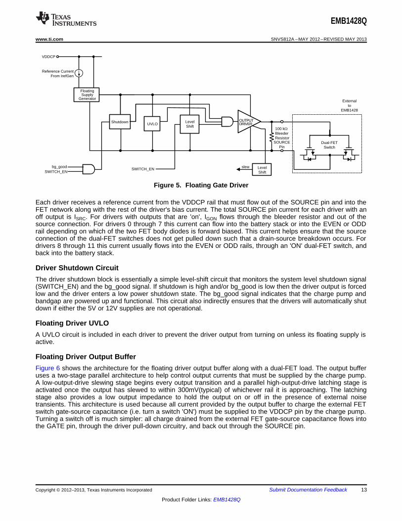
Floating Gate DriverFigure 5 shows the main blocks in the floating gate driver cell along with a dual-FET load and the built-in bleederresistor. Each of the 12 drivers has a floating supply generator, shutdown circuit, UVLO, level-shift, and outputbuffer. The SOURCE pin can be up to 60V above ground for a 14 cell pack (14X4.3V) and the GATE pin must beable to swing 12V above the SOURCE pin (in some cases above the top of the battery stack) to turn on theexternal FETs.
The internal 100k bleeder resistors ensure that the FET switches will automatically turn off in the event of acatastrophic driver failure and that the FET switches are in an off state upon system power-up. The driver isdesigned to drive the FET switch directly with no gate-source resistor.
12 Submit Documentation Feedback Copyright © 2012–2013, Texas Instruments Incorporated
Product Folder Links: EMB1428Q
Reference CurrentFrom IrefGen
VDDCP
SWITCH_ENbg_good
OUTPUTDRIVER
100 k:BleederResistor
SOURCEPin
Dual-FETSwitch
LevelShift
LevelShift
UVLOShutdown
FloatingSupply
Generator
slewSWITCH_EN
External to
EMB1428
EMB1428Q
www.ti.com SNVS812A –MAY 2012–REVISED MAY 2013
Figure 5. Floating Gate Driver
Each driver receives a reference current from the VDDCP rail that must flow out of the SOURCE pin and into theFET network along with the rest of the driver's bias current. The total SOURCE pin current for each driver with anoff output is ISRC. For drivers with outputs that are 'on', IGON flows through the bleeder resistor and out of thesource connection. For drivers 0 through 7 this current can flow into the battery stack or into the EVEN or ODDrail depending on which of the two FET body diodes is forward biased. This current helps ensure that the sourceconnection of the dual-FET switches does not get pulled down such that a drain-source breakdown occurs. Fordrivers 8 through 11 this current usually flows into the EVEN or ODD rails, through an 'ON' dual-FET switch, andback into the battery stack.
Driver Shutdown CircuitThe driver shutdown block is essentially a simple level-shift circuit that monitors the system level shutdown signal(SWITCH_EN) and the bg_good signal. If shutdown is high and/or bg_good is low then the driver output is forcedlow and the driver enters a low power shutdown state. The bg_good signal indicates that the charge pump andbandgap are powered up and functional. This circuit also indirectly ensures that the drivers will automatically shutdown if either the 5V or 12V supplies are not operational.
Floating Driver UVLOA UVLO circuit is included in each driver to prevent the driver output from turning on unless its floating supply isactive.
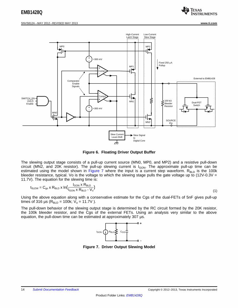
Floating Driver Output BufferFigure 6 shows the architecture for the floating driver output buffer along with a dual-FET load. The output bufferuses a two-stage parallel architecture to help control output currents that must be supplied by the charge pump.A low-output-drive slewing stage begins every output transition and a parallel high-output-drive latching stage isactivated once the output has slewed to within 300mV(typical) of whichever rail it is approaching. The latchingstage also provides a low output impedance to hold the output on or off in the presence of external noisetransients. This architecture is used because all current provided by the output buffer to charge the external FETswitch gate-source capacitance (i.e. turn a switch 'ON') must be supplied to the VDDCP pin by the charge pump.Turning a switch off is much simpler: all charge drained from the external FET gate-source capacitance flows intothe GATE pin, through the driver pull-down circuitry, and back out through the SOURCE pin.
Copyright © 2012–2013, Texas Instruments Incorporated Submit Documentation Feedback 13
Product Folder Links: EMB1428Q
RBLDIGON CGS
+
-
tSLEW = Cgs x RBLD x ln(IGON x RBLD
IGON x RBLD - Vo)
100 k:BleederResistor
Dual-FETSwitch
+-
Comp1
+
-Comp2
SWITCH_ENUVLO
Enable
Slew CurrentLevel-Shift
Slew SignaltoDigital Core
Fixed 250 PAPullup
MN1
SOURCEPin
High-CurrentLatch Stage
Low-CurrentSlew Stage
+300 mV
+300 mV+-
MP1
MP2
MN2
MP0
MN0
+
-
ComparatorEnableSignals
External to EMB1428
EMB1428Q
SNVS812A –MAY 2012–REVISED MAY 2013 www.ti.com
Figure 6. Floating Driver Output Buffer
The slewing output stage consists of a pull-up current source (MN0, MP0, and MP2) and a resistive pull-downcircuit (MN2, and 20K resistor). The pull-up slewing current is IGON. The approximate pull-up time can beestimated using the model shown in Figure 7 where the input is a current step waveform. RBLD is the 100kbleeder resistance, typical. Vo is the voltage to which the slewing stage pulls the gate voltage up to (12V-0.3V =11.7V). The equation for the slewing time is:
(1)
Using the above equation along with a conservative estimate for the Cgs of the dual-FETs of 5nF gives pull-uptimes of 316 µs (RBLD = 100k; Vo = 11.7V ).
The pull-down behavior of the slewing output stage is determined by the RC circuit formed by the 20K resistor,the 100k bleeder resistor, and the Cgs of the external FETs. Using an analysis very similar to the aboveequation, the pull-down time can be estimated at approximately 307 µs.
Figure 7. Driver Output Slewing Model
14 Submit Documentation Feedback Copyright © 2012–2013, Texas Instruments Incorporated
Product Folder Links: EMB1428Q
SOFTSTART
VDDCPCEXT2
FROM TOP OF BATTERYSTACK (60V)
CEXT1
VDDP
External to EMB1428
GNDP
CLKLVL SHIFT
VSTACK
CHARGEPUMPUVLO
C1
D2N1
D3N2
C2
C3
D1
To Digital Block
1 MHzInternal
Clock
EMB1428Q
www.ti.com SNVS812A –MAY 2012–REVISED MAY 2013
The latching output stage shown in Figure 6 consists of comparators Comp1 and Comp2 along with outputdevices MP1 and MN1. Half of this stage is de-activated each time the output begins a transition so that it doesnot conflict with the slewing stage. Comp1 and Comp2 receive an enable signal that switches them betweennormal comparator operation and a low-power mode where their outputs are forced high (Comp1) or low(Comp2) to unlatch. These comparators have a current output that is activated whenever the comparator is incomparator mode but un-latched (i.e. the output is still slewing). These currents are wire-ORed and processed bya level-shift circuit to produce a 5V logic slew signal. This slew signal is used by the digital core to control thetiming of the switch enable signals.
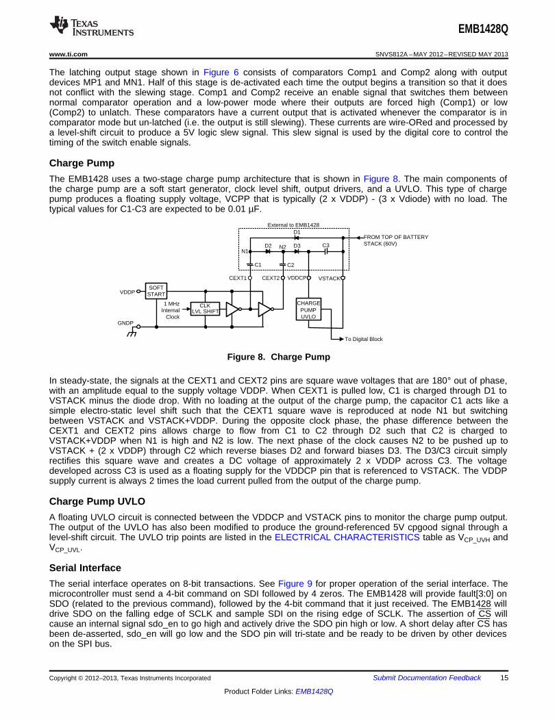
Charge PumpThe EMB1428 uses a two-stage charge pump architecture that is shown in Figure 8. The main components ofthe charge pump are a soft start generator, clock level shift, output drivers, and a UVLO. This type of chargepump produces a floating supply voltage, VCPP that is typically (2 x VDDP) - (3 x Vdiode) with no load. Thetypical values for C1-C3 are expected to be 0.01 µF.
Figure 8. Charge Pump
In steady-state, the signals at the CEXT1 and CEXT2 pins are square wave voltages that are 180° out of phase,with an amplitude equal to the supply voltage VDDP. When CEXT1 is pulled low, C1 is charged through D1 toVSTACK minus the diode drop. With no loading at the output of the charge pump, the capacitor C1 acts like asimple electro-static level shift such that the CEXT1 square wave is reproduced at node N1 but switchingbetween VSTACK and VSTACK+VDDP. During the opposite clock phase, the phase difference between theCEXT1 and CEXT2 pins allows charge to flow from C1 to C2 through D2 such that C2 is charged toVSTACK+VDDP when N1 is high and N2 is low. The next phase of the clock causes N2 to be pushed up toVSTACK + (2 x VDDP) through C2 which reverse biases D2 and forward biases D3. The D3/C3 circuit simplyrectifies this square wave and creates a DC voltage of approximately 2 x VDDP across C3. The voltagedeveloped across C3 is used as a floating supply for the VDDCP pin that is referenced to VSTACK. The VDDPsupply current is always 2 times the load current pulled from the output of the charge pump.
Charge Pump UVLOA floating UVLO circuit is connected between the VDDCP and VSTACK pins to monitor the charge pump output.The output of the UVLO has also been modified to produce the ground-referenced 5V cpgood signal through alevel-shift circuit. The UVLO trip points are listed in the ELECTRICAL CHARACTERISTICS table as VCP_UVH andVCP_UVL.
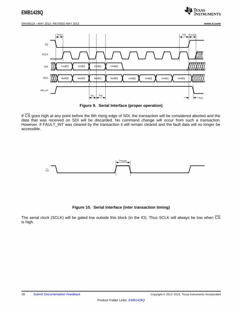
Serial InterfaceThe serial interface operates on 8-bit transactions. See Figure 9 for proper operation of the serial interface. Themicrocontroller must send a 4-bit command on SDI followed by 4 zeros. The EMB1428 will provide fault[3:0] onSDO (related to the previous command), followed by the 4-bit command that it just received. The EMB1428 willdrive SDO on the falling edge of SCLK and sample SDI on the rising edge of SCLK. The assertion of CS willcause an internal signal sdo_en to go high and actively drive the SDO pin high or low. A short delay after CS hasbeen de-asserted, sdo_en will go low and the SDO pin will tri-state and be ready to be driven by other deviceson the SPI bus.
Copyright © 2012–2013, Texas Instruments Incorporated Submit Documentation Feedback 15
Product Folder Links: EMB1428Q
tTRANS
CS
CS
SCLK
SDO
sdo_en
SDI
tCSU tHD tCDSU
tDIStHDtSU
fault[3]
cmd[3]
fault[2]
cmd[2]
fault[1]
cmd[1]
fault[0]
cmd[0]
cmd[3] cmd[2] cmd[1] cmd[0]
EMB1428Q
SNVS812A –MAY 2012–REVISED MAY 2013 www.ti.com
Figure 9. Serial Interface (proper operation)
If CS goes high at any point before the 8th rising edge of SDI, the transaction will be considered aborted and thedata that was received on SDI will be discarded. No command change will occur from such a transaction.However, if FAULT_INT was cleared by the transaction it will remain cleared and the fault data will no longer beaccessible.
Figure 10. Serial Interface (inter transaction timing)
The serial clock (SCLK) will be gated low outside this block (in the IO). Thus SCLK will always be low when CSis high.
16 Submit Documentation Feedback Copyright © 2012–2013, Texas Instruments Incorporated
Product Folder Links: EMB1428Q
SCLK
SDI cmd[3] cmd[2] cmd[1] cmd[0]
tCDSU
CS
EMB1428Q
www.ti.com SNVS812A –MAY 2012–REVISED MAY 2013
Figure 11. Serial Interface (aborted transaction)
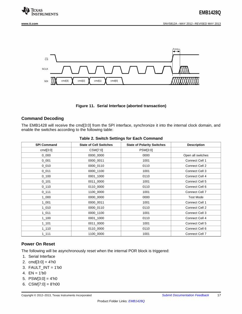
Command DecodingThe EMB1428 will receive the cmd[3:0] from the SPI interface, synchronize it into the internal clock domain, andenable the switches according to the following table:
Table 2. Switch Settings for Each CommandSPI Command State of Cell Switches State of Polarity Switches Description
cmd[3:0] CSW[7:0] PSW[3:0]0_000 0000_0000 0000 Open all switches0_001 0000_0011 1001 Connect Cell 10_010 0000_0110 0110 Connect Cell 20_011 0000_1100 1001 Connect Cell 30_100 0001_1000 0110 Connect Cell 40_101 0011_0000 1001 Connect Cell 50_110 0110_0000 0110 Connect Cell 60_111 1100_0000 1001 Connect Cell 71_000 0000_0000 0000 Test Mode1_001 0000_0011 1001 Connect Cell 11_010 0000_0110 0110 Connect Cell 21_011 0000_1100 1001 Connect Cell 31_100 0001_1000 0110 Connect Cell 41_101 0011_0000 1001 Connect Cell 51_110 0110_0000 0110 Connect Cell 61_111 1100_0000 1001 Connect Cell 7
Power On ResetThe following will be asynchronously reset when the internal POR block is triggered:1. Serial Interface2. cmd[3:0] = 4’h03. FAULT_INT = 1’b04. EN = 1’b05. PSW[3:0] = 4’h06. CSW[7:0] = 8’h00
Copyright © 2012–2013, Texas Instruments Incorporated Submit Documentation Feedback 17
Product Folder Links: EMB1428Q
START CommandProcessed
Enable FET Switches for Selected Cell
Wait for new command
Internal Fault Checking
DONE set unexpectedlySet FAULT_INT
output
Set DIR, check DIR_RT
Set ENDONE set
Read FAULT Pins
Reset EN, Wait for DONE
Open all FET Switches
SLEEP
STOP CommandProcessed
30176820
EMB1428Q
SNVS812A –MAY 2012–REVISED MAY 2013 www.ti.com
7. Shutdown Mode = yes8. Internal Clock = off9. Normal Mode/Test Mode = Normal Mode
The serial interface is reset so that it is prepared to detect aborted transactions. If POR block isn’t triggered, theserial interface will still function. However the initial state of the part will be unknown, so the first transaction mayclock out a fault code.
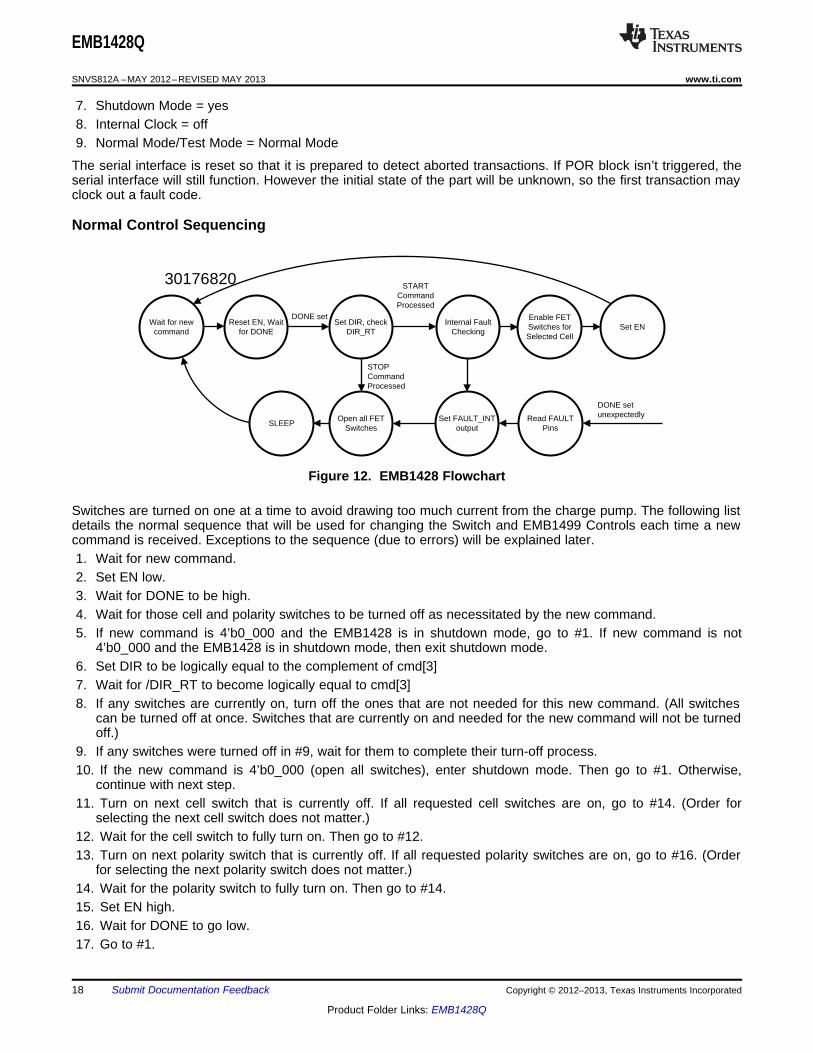
Normal Control Sequencing
Figure 12. EMB1428 Flowchart
Switches are turned on one at a time to avoid drawing too much current from the charge pump. The following listdetails the normal sequence that will be used for changing the Switch and EMB1499 Controls each time a newcommand is received. Exceptions to the sequence (due to errors) will be explained later.1. Wait for new command.2. Set EN low.3. Wait for DONE to be high.4. Wait for those cell and polarity switches to be turned off as necessitated by the new command.5. If new command is 4’b0_000 and the EMB1428 is in shutdown mode, go to #1. If new command is not
4’b0_000 and the EMB1428 is in shutdown mode, then exit shutdown mode.6. Set DIR to be logically equal to the complement of cmd[3]7. Wait for /DIR_RT to become logically equal to cmd[3]8. If any switches are currently on, turn off the ones that are not needed for this new command. (All switches
can be turned off at once. Switches that are currently on and needed for the new command will not be turnedoff.)
9. If any switches were turned off in #9, wait for them to complete their turn-off process.10. If the new command is 4’b0_000 (open all switches), enter shutdown mode. Then go to #1. Otherwise,
continue with next step.11. Turn on next cell switch that is currently off. If all requested cell switches are on, go to #14. (Order for
selecting the next cell switch does not matter.)12. Wait for the cell switch to fully turn on. Then go to #12.13. Turn on next polarity switch that is currently off. If all requested polarity switches are on, go to #16. (Order
for selecting the next polarity switch does not matter.)14. Wait for the polarity switch to fully turn on. Then go to #14.15. Set EN high.16. Wait for DONE to go low.17. Go to #1.
18 Submit Documentation Feedback Copyright © 2012–2013, Texas Instruments Incorporated
Product Folder Links: EMB1428Q
tDIR
EN
tDIR
DIR_RT
DIR
tDIRSU tDIRSU
EMB1428Q
www.ti.com SNVS812A –MAY 2012–REVISED MAY 2013
Any time a new command arrives, the EMB1428 immediately goes back to step #2, regardless of where it was atin the sequence. Any time an error occurs that causes FAULT_INT to go high, the EMB1428 immediately goesback to step #1 and acts as if it received a command to open all switches.
Emergency ShutdownIf the EMB1428 receives two consecutive commands to open all switches (no intervening commands), it willimmediately set CSW[7:0], PSW[3:0] = 12’h0. This allows all switches to be shut off if there is a problem in theEMB1499 communication or in the EMB1428 charge pump circuitry.
An emergency shutdown will cause the EMB1428 to enter shutdown mode and turn off its internal clock within afew clock cycles without waiting for switches to finish turning on or off.
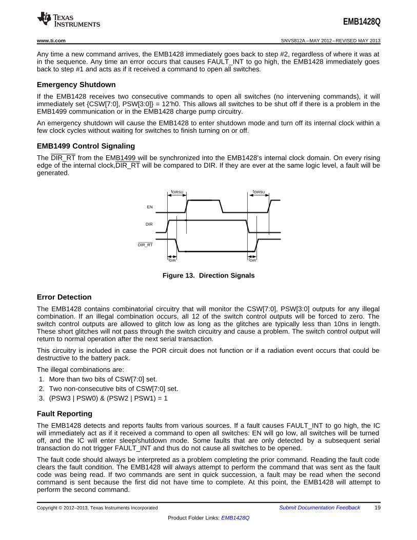
EMB1499 Control SignalingThe DIR_RT from the EMB1499 will be synchronized into the EMB1428’s internal clock domain. On every risingedge of the internal clock,DIR_RT will be compared to DIR. If they are ever at the same logic level, a fault will begenerated.
Figure 13. Direction Signals
Error DetectionThe EMB1428 contains combinatorial circuitry that will monitor the CSW[7:0], PSW[3:0] outputs for any illegalcombination. If an illegal combination occurs, all 12 of the switch control outputs will be forced to zero. Theswitch control outputs are allowed to glitch low as long as the glitches are typically less than 10ns in length.These short glitches will not pass through the switch circuitry and cause a problem. The switch control output willreturn to normal operation after the next serial transaction.
This circuitry is included in case the POR circuit does not function or if a radiation event occurs that could bedestructive to the battery pack.
The illegal combinations are:1. More than two bits of CSW[7:0] set.2. Two non-consecutive bits of CSW[7:0] set.3. (PSW3 | PSW0) & (PSW2 | PSW1) = 1
Fault ReportingThe EMB1428 detects and reports faults from various sources. If a fault causes FAULT_INT to go high, the ICwill immediately act as if it received a command to open all switches: EN will go low, all switches will be turnedoff, and the IC will enter sleep/shutdown mode. Some faults that are only detected by a subsequent serialtransaction do not trigger FAULT_INT and thus do not cause all switches to be opened.
The fault code should always be interpreted as a problem completing the prior command. Reading the fault codeclears the fault condition. The EMB1428 will always attempt to perform the command that was sent as the faultcode was being read. If two commands are sent in quick succession, a fault may be read when the secondcommand is sent because the first did not have time to complete. At this point, the EMB1428 will attempt toperform the second command.
Copyright © 2012–2013, Texas Instruments Incorporated Submit Documentation Feedback 19
Product Folder Links: EMB1428Q
SCLK
SDI cmd[3] cmd[2] cmd[1] cmd[0]
tINT
CS
FAULT_INT
SCLK
FAULT_INT
tINT
CS
EMB1428Q
SNVS812A –MAY 2012–REVISED MAY 2013 www.ti.com
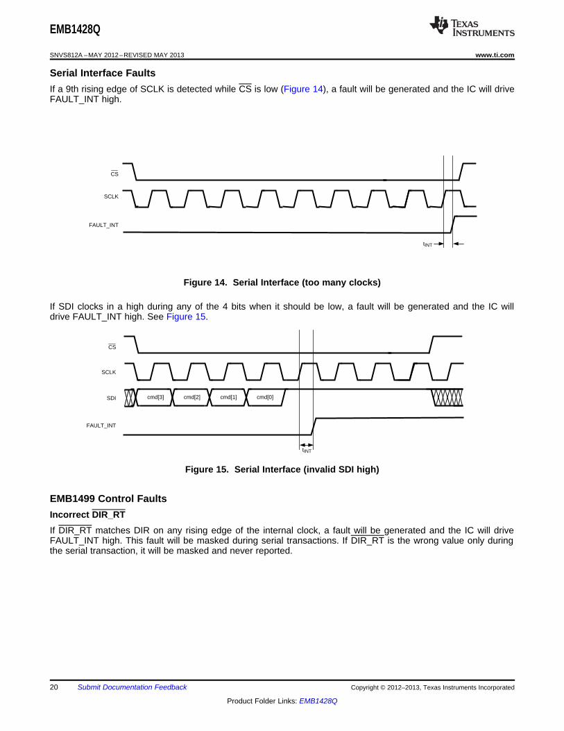
Serial Interface FaultsIf a 9th rising edge of SCLK is detected while CS is low (Figure 14), a fault will be generated and the IC will driveFAULT_INT high.
Figure 14. Serial Interface (too many clocks)
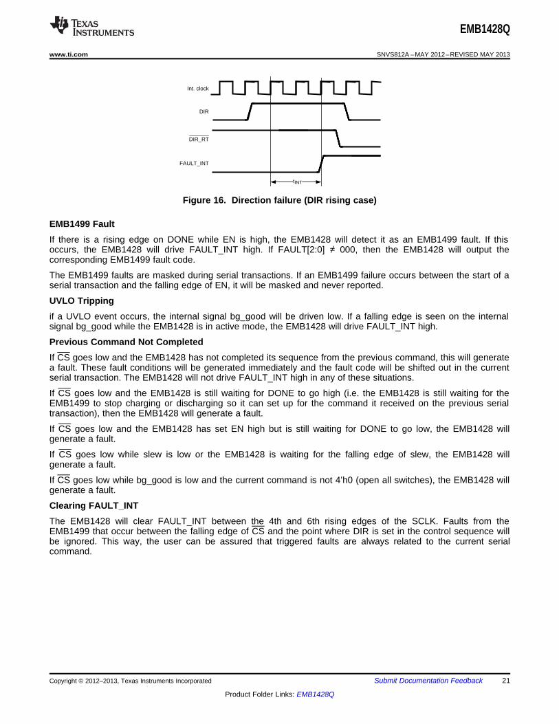
If SDI clocks in a high during any of the 4 bits when it should be low, a fault will be generated and the IC willdrive FAULT_INT high. See Figure 15.
Figure 15. Serial Interface (invalid SDI high)
EMB1499 Control FaultsIncorrect DIR_RTIf DIR_RT matches DIR on any rising edge of the internal clock, a fault will be generated and the IC will driveFAULT_INT high. This fault will be masked during serial transactions. If DIR_RT is the wrong value only duringthe serial transaction, it will be masked and never reported.
20 Submit Documentation Feedback Copyright © 2012–2013, Texas Instruments Incorporated
Product Folder Links: EMB1428Q
FAULT_INT
tINT
DIR_RT
Int. clock
DIR
EMB1428Q
www.ti.com SNVS812A –MAY 2012–REVISED MAY 2013
Figure 16. Direction failure (DIR rising case)
EMB1499 FaultIf there is a rising edge on DONE while EN is high, the EMB1428 will detect it as an EMB1499 fault. If thisoccurs, the EMB1428 will drive FAULT_INT high. If FAULT[2:0] ≠ 000, then the EMB1428 will output thecorresponding EMB1499 fault code.
The EMB1499 faults are masked during serial transactions. If an EMB1499 failure occurs between the start of aserial transaction and the falling edge of EN, it will be masked and never reported.
UVLO Trippingif a UVLO event occurs, the internal signal bg_good will be driven low. If a falling edge is seen on the internalsignal bg_good while the EMB1428 is in active mode, the EMB1428 will drive FAULT_INT high.
Previous Command Not CompletedIf CS goes low and the EMB1428 has not completed its sequence from the previous command, this will generatea fault. These fault conditions will be generated immediately and the fault code will be shifted out in the currentserial transaction. The EMB1428 will not drive FAULT_INT high in any of these situations.
If CS goes low and the EMB1428 is still waiting for DONE to go high (i.e. the EMB1428 is still waiting for theEMB1499 to stop charging or discharging so it can set up for the command it received on the previous serialtransaction), then the EMB1428 will generate a fault.
If CS goes low and the EMB1428 has set EN high but is still waiting for DONE to go low, the EMB1428 willgenerate a fault.
If CS goes low while slew is low or the EMB1428 is waiting for the falling edge of slew, the EMB1428 willgenerate a fault.
If CS goes low while bg_good is low and the current command is not 4’h0 (open all switches), the EMB1428 willgenerate a fault.
Clearing FAULT_INTThe EMB1428 will clear FAULT_INT between the 4th and 6th rising edges of the SCLK. Faults from theEMB1499 that occur between the falling edge of CS and the point where DIR is set in the control sequence willbe ignored. This way, the user can be assured that triggered faults are always related to the current serialcommand.
Copyright © 2012–2013, Texas Instruments Incorporated Submit Documentation Feedback 21
Product Folder Links: EMB1428Q
SCLK
SDI cmd[3] cmd[2] cmd[1] cmd[0]
CS
FAULT_INT
EMB1428Q
SNVS812A –MAY 2012–REVISED MAY 2013 www.ti.com
Figure 17. Clearing FAULT_INT
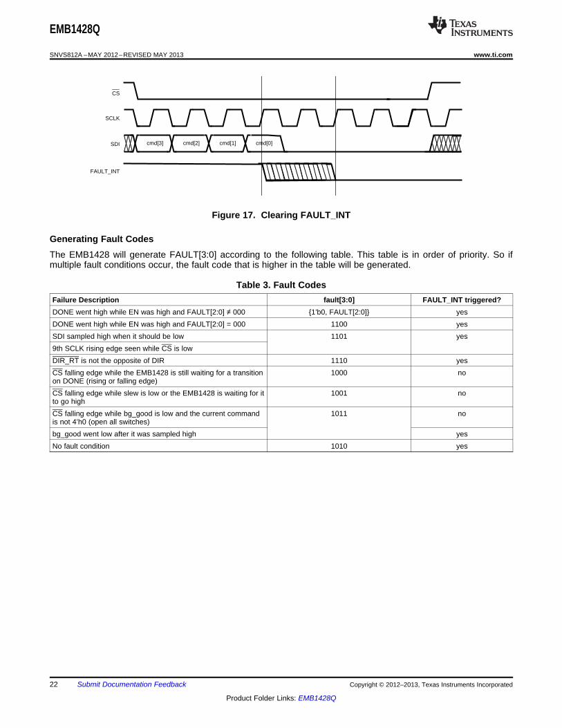
Generating Fault CodesThe EMB1428 will generate FAULT[3:0] according to the following table. This table is in order of priority. So ifmultiple fault conditions occur, the fault code that is higher in the table will be generated.
Table 3. Fault CodesFailure Description fault[3:0] FAULT_INT triggered?DONE went high while EN was high and FAULT[2:0] ≠ 000 1’b0, FAULT[2:0] yesDONE went high while EN was high and FAULT[2:0] = 000 1100 yesSDI sampled high when it should be low 1101 yes9th SCLK rising edge seen while CS is lowDIR_RT is not the opposite of DIR 1110 yesCS falling edge while the EMB1428 is still waiting for a transition 1000 noon DONE (rising or falling edge)CS falling edge while slew is low or the EMB1428 is waiting for it 1001 noto go highCS falling edge while bg_good is low and the current command 1011 nois not 4’h0 (open all switches)bg_good went low after it was sampled high yesNo fault condition 1010 yes
22 Submit Documentation Feedback Copyright © 2012–2013, Texas Instruments Incorporated
Product Folder Links: EMB1428Q
EMB1428Q
www.ti.com SNVS812A –MAY 2012–REVISED MAY 2013
REVISION HISTORY
Changes from Original (April 2013) to Revision A Page
• Changed layout of National Data Sheet to TI format .......................................................................................................... 22
Copyright © 2012–2013, Texas Instruments Incorporated Submit Documentation Feedback 23
Product Folder Links: EMB1428Q
PACKAGE OPTION ADDENDUM
www.ti.com 18-Dec-2013
Addendum-Page 1
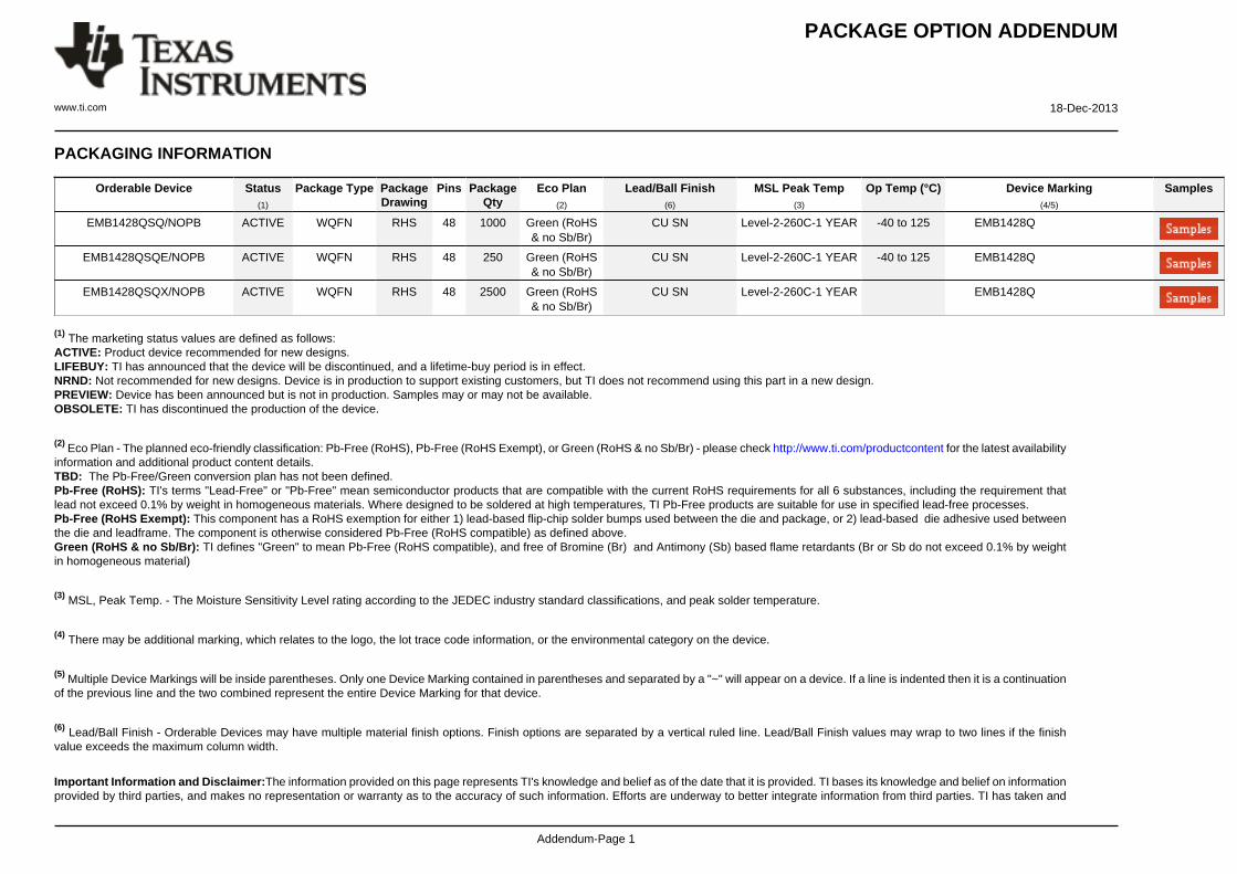
PACKAGING INFORMATION
Orderable Device Status(1)
Package Type PackageDrawing
Pins PackageQty
Eco Plan(2)
Lead/Ball Finish(6)
MSL Peak Temp(3)
Op Temp (°C) Device Marking(4/5)
Samples
EMB1428QSQ/NOPB ACTIVE WQFN RHS 48 1000 Green (RoHS& no Sb/Br)
CU SN Level-2-260C-1 YEAR -40 to 125 EMB1428Q
EMB1428QSQE/NOPB ACTIVE WQFN RHS 48 250 Green (RoHS& no Sb/Br)
CU SN Level-2-260C-1 YEAR -40 to 125 EMB1428Q
EMB1428QSQX/NOPB ACTIVE WQFN RHS 48 2500 Green (RoHS& no Sb/Br)
CU SN Level-2-260C-1 YEAR EMB1428Q
(1) The marketing status values are defined as follows:ACTIVE: Product device recommended for new designs.LIFEBUY: TI has announced that the device will be discontinued, and a lifetime-buy period is in effect.NRND: Not recommended for new designs. Device is in production to support existing customers, but TI does not recommend using this part in a new design.PREVIEW: Device has been announced but is not in production. Samples may or may not be available.OBSOLETE: TI has discontinued the production of the device.
(2) Eco Plan - The planned eco-friendly classification: Pb-Free (RoHS), Pb-Free (RoHS Exempt), or Green (RoHS & no Sb/Br) - please check http://www.ti.com/productcontent for the latest availabilityinformation and additional product content details.TBD: The Pb-Free/Green conversion plan has not been defined.Pb-Free (RoHS): TI's terms "Lead-Free" or "Pb-Free" mean semiconductor products that are compatible with the current RoHS requirements for all 6 substances, including the requirement thatlead not exceed 0.1% by weight in homogeneous materials. Where designed to be soldered at high temperatures, TI Pb-Free products are suitable for use in specified lead-free processes.Pb-Free (RoHS Exempt): This component has a RoHS exemption for either 1) lead-based flip-chip solder bumps used between the die and package, or 2) lead-based die adhesive used betweenthe die and leadframe. The component is otherwise considered Pb-Free (RoHS compatible) as defined above.Green (RoHS & no Sb/Br): TI defines "Green" to mean Pb-Free (RoHS compatible), and free of Bromine (Br) and Antimony (Sb) based flame retardants (Br or Sb do not exceed 0.1% by weightin homogeneous material)
(3) MSL, Peak Temp. - The Moisture Sensitivity Level rating according to the JEDEC industry standard classifications, and peak solder temperature.
(4) There may be additional marking, which relates to the logo, the lot trace code information, or the environmental category on the device.
(5) Multiple Device Markings will be inside parentheses. Only one Device Marking contained in parentheses and separated by a "~" will appear on a device. If a line is indented then it is a continuationof the previous line and the two combined represent the entire Device Marking for that device.
(6) Lead/Ball Finish - Orderable Devices may have multiple material finish options. Finish options are separated by a vertical ruled line. Lead/Ball Finish values may wrap to two lines if the finishvalue exceeds the maximum column width.
Important Information and Disclaimer:The information provided on this page represents TI's knowledge and belief as of the date that it is provided. TI bases its knowledge and belief on informationprovided by third parties, and makes no representation or warranty as to the accuracy of such information. Efforts are underway to better integrate information from third parties. TI has taken and
PACKAGE OPTION ADDENDUM
www.ti.com 18-Dec-2013
Addendum-Page 2
continues to take reasonable steps to provide representative and accurate information but may not have conducted destructive testing or chemical analysis on incoming materials and chemicals.TI and TI suppliers consider certain information to be proprietary, and thus CAS numbers and other limited information may not be available for release.
In no event shall TI's liability arising out of such information exceed the total purchase price of the TI part(s) at issue in this document sold by TI to Customer on an annual basis.
TAPE AND REEL INFORMATION
*All dimensions are nominal
Device PackageType
PackageDrawing
Pins SPQ ReelDiameter
(mm)
ReelWidth
W1 (mm)
A0(mm)
B0(mm)
K0(mm)
P1(mm)
W(mm)
Pin1Quadrant
EMB1428QSQ/NOPB WQFN RHS 48 1000 330.0 16.4 7.3 7.3 1.3 12.0 16.0 Q1
EMB1428QSQE/NOPB WQFN RHS 48 250 178.0 16.4 7.3 7.3 1.3 12.0 16.0 Q1
EMB1428QSQX/NOPB WQFN RHS 48 2500 330.0 16.4 7.3 7.3 1.3 12.0 16.0 Q1
PACKAGE MATERIALS INFORMATION
www.ti.com 20-Sep-2016
Pack Materials-Page 1
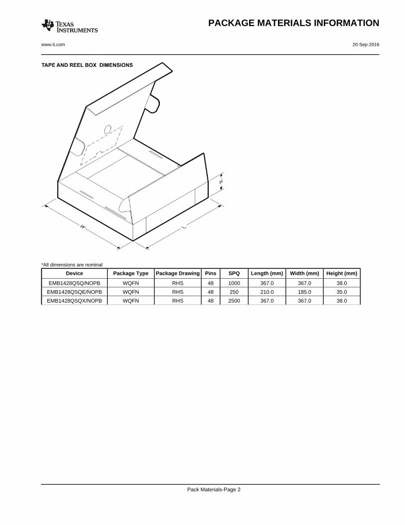
*All dimensions are nominal
Device Package Type Package Drawing Pins SPQ Length (mm) Width (mm) Height (mm)
EMB1428QSQ/NOPB WQFN RHS 48 1000 367.0 367.0 38.0
EMB1428QSQE/NOPB WQFN RHS 48 250 210.0 185.0 35.0
EMB1428QSQX/NOPB WQFN RHS 48 2500 367.0 367.0 38.0
PACKAGE MATERIALS INFORMATION
www.ti.com 20-Sep-2016
Pack Materials-Page 2
www.ti.com
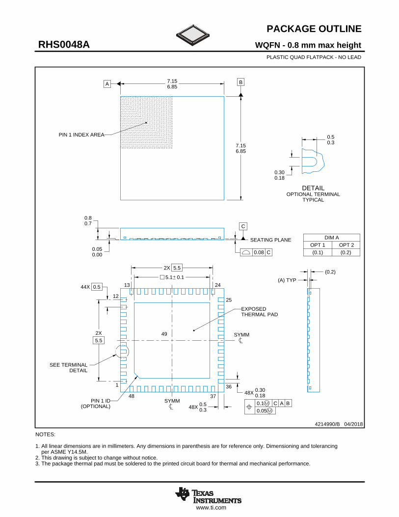
PACKAGE OUTLINE
C
SEE TERMINALDETAIL
48X 0.300.18
5.1 0.1
48X 0.50.3
0.80.7
(A) TYP
0.050.00
44X 0.5
2X5.5
2X 5.5
A 7.156.85
B
7.156.85
0.300.18
0.50.3
(0.2)
WQFN - 0.8 mm max heightRHS0048APLASTIC QUAD FLATPACK - NO LEAD
4214990/B 04/2018
DIM AOPT 1 OPT 2(0.1) (0.2)
PIN 1 INDEX AREA
0.08 C
SEATING PLANE
1
1225
36
13 24
48 37
(OPTIONAL)PIN 1 ID 0.1 C A B
0.05
EXPOSEDTHERMAL PAD
49 SYMM
SYMM
NOTES: 1. All linear dimensions are in millimeters. Any dimensions in parenthesis are for reference only. Dimensioning and tolerancing per ASME Y14.5M. 2. This drawing is subject to change without notice. 3. The package thermal pad must be soldered to the printed circuit board for thermal and mechanical performance.
SCALE 1.800
DETAILOPTIONAL TERMINAL
TYPICAL
www.ti.com
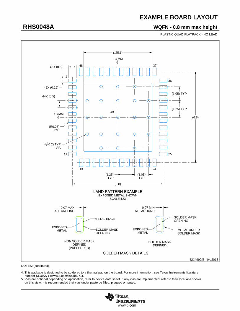
EXAMPLE BOARD LAYOUT
0.07 MINALL AROUND
0.07 MAXALL AROUND
48X (0.25)
48X (0.6)
( 0.2) TYPVIA
44X (0.5)
(6.8)
(6.8)
(1.25) TYP
( 5.1)
(R0.05)TYP
(1.25)TYP
(1.05) TYP
(1.05)TYP
WQFN - 0.8 mm max heightRHS0048APLASTIC QUAD FLATPACK - NO LEAD
4214990/B 04/2018
SYMM
1
12
13 24
25
36
3748
SYMM
LAND PATTERN EXAMPLEEXPOSED METAL SHOWN
SCALE:12X
NOTES: (continued) 4. This package is designed to be soldered to a thermal pad on the board. For more information, see Texas Instruments literature number SLUA271 (www.ti.com/lit/slua271).5. Vias are optional depending on application, refer to device data sheet. If any vias are implemented, refer to their locations shown on this view. It is recommended that vias under paste be filled, plugged or tented.
49
SOLDER MASKOPENING
METAL UNDERSOLDER MASK
SOLDER MASKDEFINED
EXPOSEDMETAL
METAL EDGE
SOLDER MASKOPENING
SOLDER MASK DETAILS
NON SOLDER MASKDEFINED
(PREFERRED)
EXPOSEDMETAL
www.ti.com
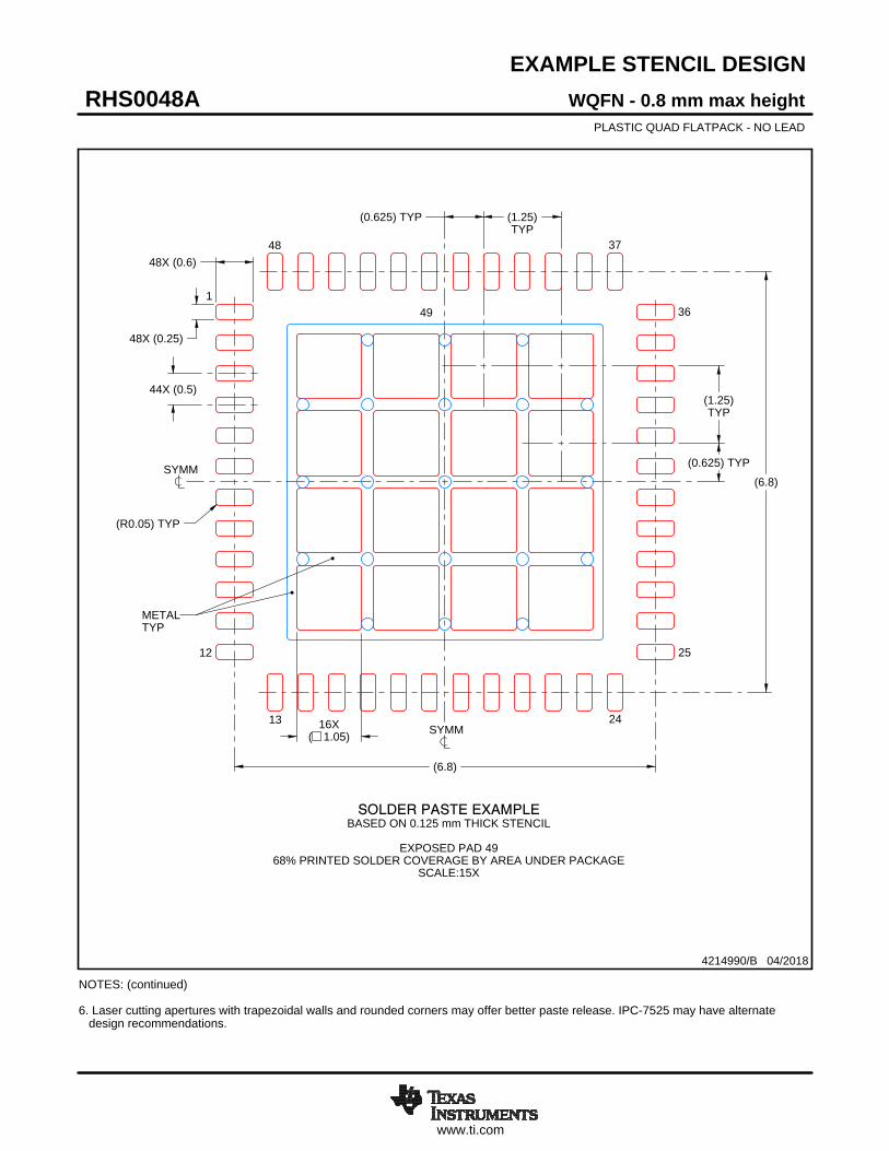
EXAMPLE STENCIL DESIGN
48X (0.6)
48X (0.25)
44X (0.5)
(6.8)
(6.8)
16X( 1.05)
(0.625) TYP
(R0.05) TYP
(1.25)TYP
(1.25)TYP
(0.625) TYP
WQFN - 0.8 mm max heightRHS0048APLASTIC QUAD FLATPACK - NO LEAD
4214990/B 04/2018
NOTES: (continued) 6. Laser cutting apertures with trapezoidal walls and rounded corners may offer better paste release. IPC-7525 may have alternate design recommendations.
49
SYMM
METALTYP
SOLDER PASTE EXAMPLEBASED ON 0.125 mm THICK STENCIL
EXPOSED PAD 49
68% PRINTED SOLDER COVERAGE BY AREA UNDER PACKAGESCALE:15X
SYMM
1
12
13 24
25
36
3748
IMPORTANT NOTICE
Texas Instruments Incorporated (TI) reserves the right to make corrections, enhancements, improvements and other changes to itssemiconductor products and services per JESD46, latest issue, and to discontinue any product or service per JESD48, latest issue. Buyersshould obtain the latest relevant information before placing orders and should verify that such information is current and complete.TI’s published terms of sale for semiconductor products (http://www.ti.com/sc/docs/stdterms.htm) apply to the sale of packaged integratedcircuit products that TI has qualified and released to market. Additional terms may apply to the use or sale of other types of TI products andservices.Reproduction of significant portions of TI information in TI data sheets is permissible only if reproduction is without alteration and isaccompanied by all associated warranties, conditions, limitations, and notices. TI is not responsible or liable for such reproduceddocumentation. Information of third parties may be subject to additional restrictions. Resale of TI products or services with statementsdifferent from or beyond the parameters stated by TI for that product or service voids all express and any implied warranties for theassociated TI product or service and is an unfair and deceptive business practice. TI is not responsible or liable for any such statements.Buyers and others who are developing systems that incorporate TI products (collectively, “Designers”) understand and agree that Designersremain responsible for using their independent analysis, evaluation and judgment in designing their applications and that Designers havefull and exclusive responsibility to assure the safety of Designers' applications and compliance of their applications (and of all TI productsused in or for Designers’ applications) with all applicable regulations, laws and other applicable requirements. Designer represents that, withrespect to their applications, Designer has all the necessary expertise to create and implement safeguards that (1) anticipate dangerousconsequences of failures, (2) monitor failures and their consequences, and (3) lessen the likelihood of failures that might cause harm andtake appropriate actions. Designer agrees that prior to using or distributing any applications that include TI products, Designer willthoroughly test such applications and the functionality of such TI products as used in such applications.TI’s provision of technical, application or other design advice, quality characterization, reliability data or other services or information,including, but not limited to, reference designs and materials relating to evaluation modules, (collectively, “TI Resources”) are intended toassist designers who are developing applications that incorporate TI products; by downloading, accessing or using TI Resources in anyway, Designer (individually or, if Designer is acting on behalf of a company, Designer’s company) agrees to use any particular TI Resourcesolely for this purpose and subject to the terms of this Notice.TI’s provision of TI Resources does not expand or otherwise alter TI’s applicable published warranties or warranty disclaimers for TIproducts, and no additional obligations or liabilities arise from TI providing such TI Resources. TI reserves the right to make corrections,enhancements, improvements and other changes to its TI Resources. TI has not conducted any testing other than that specificallydescribed in the published documentation for a particular TI Resource.Designer is authorized to use, copy and modify any individual TI Resource only in connection with the development of applications thatinclude the TI product(s) identified in such TI Resource. NO OTHER LICENSE, EXPRESS OR IMPLIED, BY ESTOPPEL OR OTHERWISETO ANY OTHER TI INTELLECTUAL PROPERTY RIGHT, AND NO LICENSE TO ANY TECHNOLOGY OR INTELLECTUAL PROPERTYRIGHT OF TI OR ANY THIRD PARTY IS GRANTED HEREIN, including but not limited to any patent right, copyright, mask work right, orother intellectual property right relating to any combination, machine, or process in which TI products or services are used. Informationregarding or referencing third-party products or services does not constitute a license to use such products or services, or a warranty orendorsement thereof. Use of TI Resources may require a license from a third party under the patents or other intellectual property of thethird party, or a license from TI under the patents or other intellectual property of TI.TI RESOURCES ARE PROVIDED “AS IS” AND WITH ALL FAULTS. TI DISCLAIMS ALL OTHER WARRANTIES ORREPRESENTATIONS, EXPRESS OR IMPLIED, REGARDING RESOURCES OR USE THEREOF, INCLUDING BUT NOT LIMITED TOACCURACY OR COMPLETENESS, TITLE, ANY EPIDEMIC FAILURE WARRANTY AND ANY IMPLIED WARRANTIES OFMERCHANTABILITY, FITNESS FOR A PARTICULAR PURPOSE, AND NON-INFRINGEMENT OF ANY THIRD PARTY INTELLECTUALPROPERTY RIGHTS. TI SHALL NOT BE LIABLE FOR AND SHALL NOT DEFEND OR INDEMNIFY DESIGNER AGAINST ANY CLAIM,INCLUDING BUT NOT LIMITED TO ANY INFRINGEMENT CLAIM THAT RELATES TO OR IS BASED ON ANY COMBINATION OFPRODUCTS EVEN IF DESCRIBED IN TI RESOURCES OR OTHERWISE. IN NO EVENT SHALL TI BE LIABLE FOR ANY ACTUAL,DIRECT, SPECIAL, COLLATERAL, INDIRECT, PUNITIVE, INCIDENTAL, CONSEQUENTIAL OR EXEMPLARY DAMAGES INCONNECTION WITH OR ARISING OUT OF TI RESOURCES OR USE THEREOF, AND REGARDLESS OF WHETHER TI HAS BEENADVISED OF THE POSSIBILITY OF SUCH DAMAGES.Unless TI has explicitly designated an individual product as meeting the requirements of a particular industry standard (e.g., ISO/TS 16949and ISO 26262), TI is not responsible for any failure to meet such industry standard requirements.Where TI specifically promotes products as facilitating functional safety or as compliant with industry functional safety standards, suchproducts are intended to help enable customers to design and create their own applications that meet applicable functional safety standardsand requirements. Using products in an application does not by itself establish any safety features in the application. Designers mustensure compliance with safety-related requirements and standards applicable to their applications. Designer may not use any TI products inlife-critical medical equipment unless authorized officers of the parties have executed a special contract specifically governing such use.Life-critical medical equipment is medical equipment where failure of such equipment would cause serious bodily injury or death (e.g., lifesupport, pacemakers, defibrillators, heart pumps, neurostimulators, and implantables). Such equipment includes, without limitation, allmedical devices identified by the U.S. Food and Drug Administration as Class III devices and equivalent classifications outside the U.S.TI may expressly designate certain products as completing a particular qualification (e.g., Q100, Military Grade, or Enhanced Product).Designers agree that it has the necessary expertise to select the product with the appropriate qualification designation for their applicationsand that proper product selection is at Designers’ own risk. Designers are solely responsible for compliance with all legal and regulatoryrequirements in connection with such selection.Designer will fully indemnify TI and its representatives against any damages, costs, losses, and/or liabilities arising out of Designer’s non-compliance with the terms and provisions of this Notice.
Mailing Address: Texas Instruments, Post Office Box 655303, Dallas, Texas 75265Copyright © 2018, Texas Instruments Incorporated