EM Effects on Semiconductor Devices, Gates and …EM Effects on Semiconductor Devices, ... coupling...
48
EM Effects on Semiconductor Devices, Gates and Integrated Circuit Interconnects Dept. of Electrical and Computer Engineering, UMCP Neil Goldsman Collaborators: Omar Ramahi, John Rogers, Bruce Jacob, Agis Iliadis Xi Shao, Parvez N. Guzdar Akin Akturk, Zeynep Dilli, Bo Yang, Todd Firestone
Transcript of EM Effects on Semiconductor Devices, Gates and …EM Effects on Semiconductor Devices, ... coupling...
EM Effects on Semiconductor Devices, Gates and Integrated Circuit
InterconnectsDept. of Electrical and Computer Engineering, UMCP
Neil Goldsman
Collaborators:Omar Ramahi, John Rogers, Bruce Jacob, Agis Iliadis
Xi Shao, Parvez N. GuzdarAkin Akturk, Zeynep Dilli, Bo Yang, Todd Firestone
EM Effects on Semiconductor Devices, Gates and Integrated Circuit Interconnects
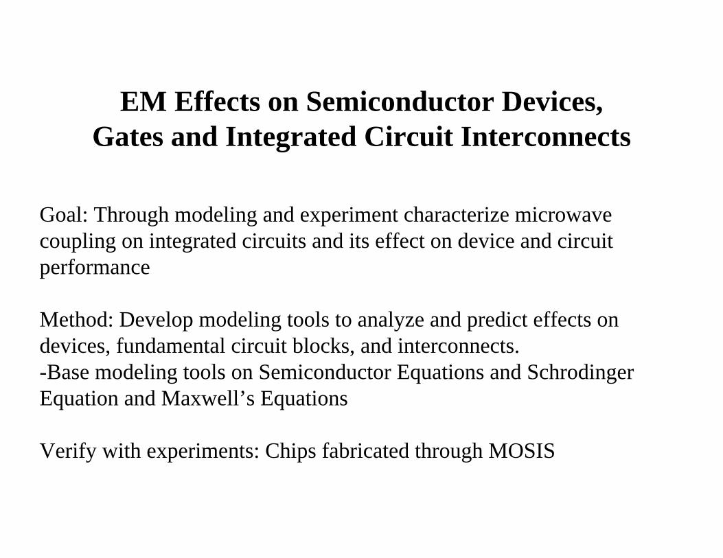
Goal: Through modeling and experiment characterize microwave coupling on integrated circuits and its effect on device and circuit performance
Method: Develop modeling tools to analyze and predict effects ondevices, fundamental circuit blocks, and interconnects.-Base modeling tools on Semiconductor Equations and SchrodingerEquation and Maxwell’s Equations
Verify with experiments: Chips fabricated through MOSIS
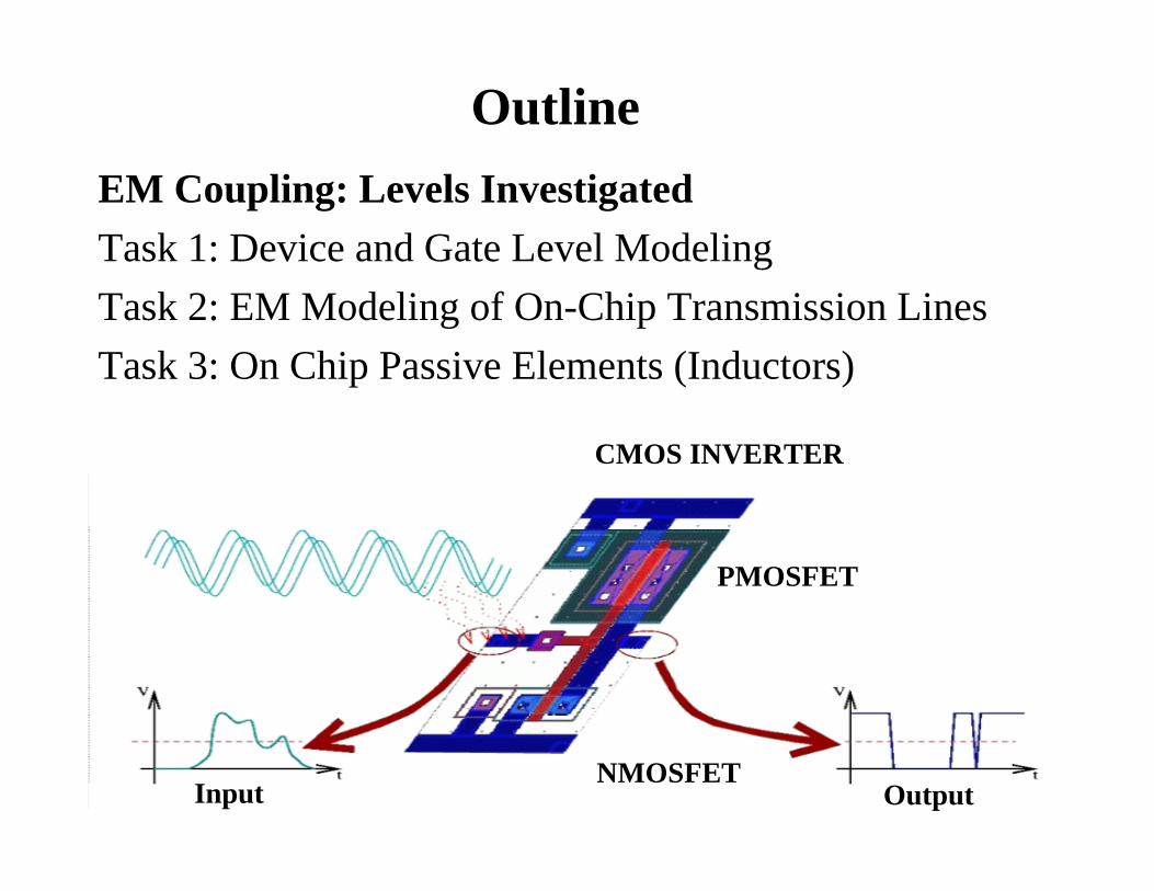
OutlineEM Coupling: Levels InvestigatedTask 1: Device and Gate Level ModelingTask 2: EM Modeling of On-Chip Transmission LinesTask 3: On Chip Passive Elements (Inductors)
PMOSFET
NMOSFET
CMOS INVERTER
Input Output
Task 1: EM Coupling to Semiconductor Devices
• EM coupling may induce large voltages on semiconductor device terminals inside IC’s
• Large terminal voltages can damage devices permanently and cause upsets.
• Most modern ICs are composed of MOSFETs.• Pentium IV contains 40 million nanoscale MOSFETs.• MOSFETs are exceptionally vulnerable.• Task 1 focuses on detailed modeling of MOSFETs to
understand their internal mechanisms of EM induced failure.

MOSFET Cross-Section and Illustration of Vulnerabilities:Oxide and Avalanche Breakdown
Current through the gate
Problems:-Scaling to the nanometer gate length requires oxides less than 20Angstroms.-Such thin oxides give rise to such large gate current that devices will not function.-Large internal fields cause impact ionization, avalanching and damaging filaments-Problems especially important for EM coupling, which induces large voltages to Gate and Drain Electrodes!
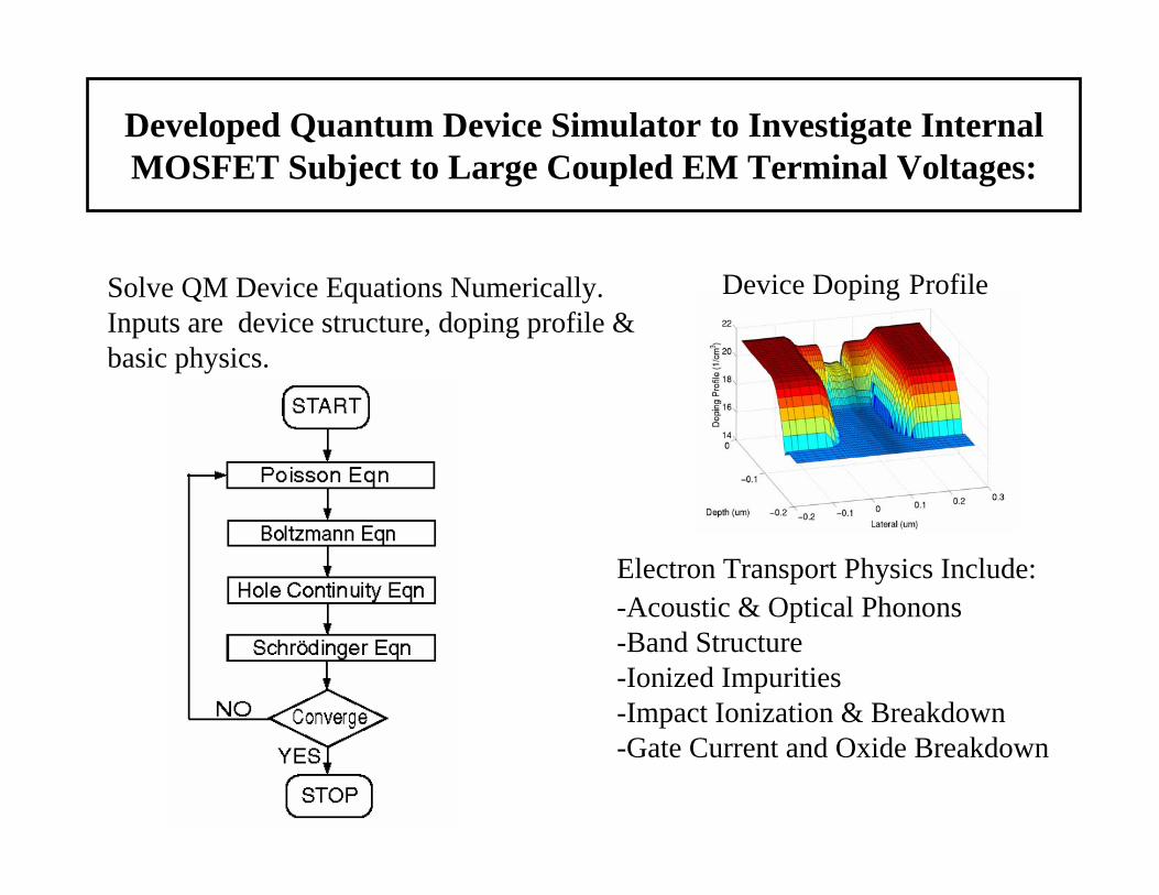
Developed Quantum Device Simulator to Investigate Internal MOSFET Subject to Large Coupled EM Terminal Voltages:
Device Doping ProfileSolve QM Device Equations Numerically.Inputs are device structure, doping profile & basic physics.
Electron Transport Physics Include:-Acoustic & Optical Phonons-Band Structure-Ionized Impurities-Impact Ionization & Breakdown-Gate Current and Oxide Breakdown
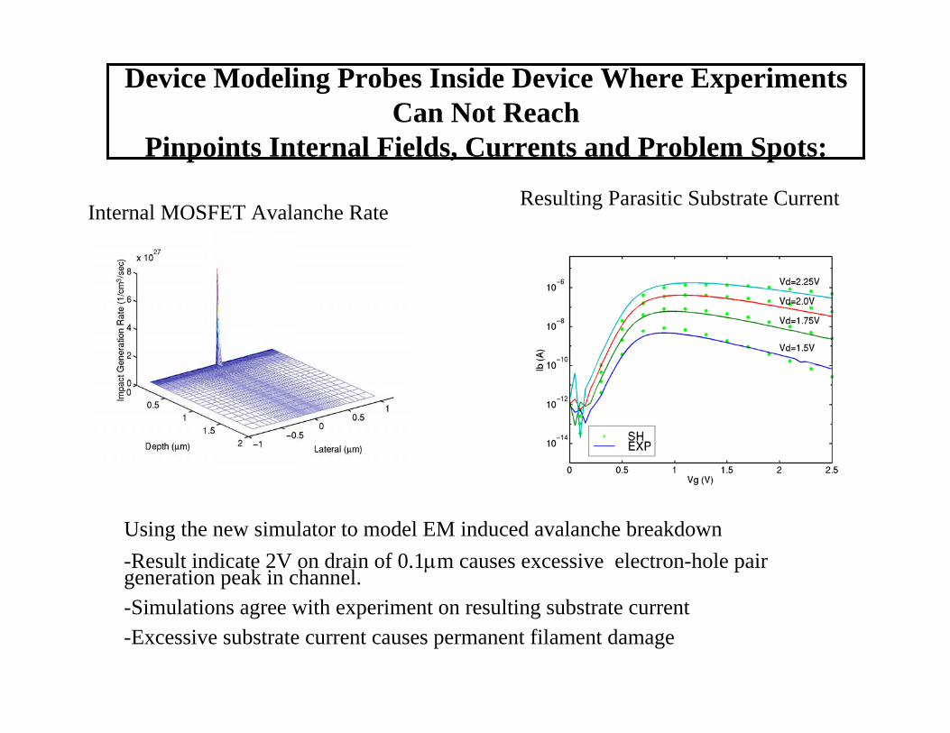
Device Modeling Probes Inside Device Where Experiments Can Not Reach
Pinpoints Internal Fields, Currents and Problem Spots:
Internal MOSFET Avalanche Rate Resulting Parasitic Substrate Current
Using the new simulator to model EM induced avalanche breakdown-Result indicate 2V on drain of 0.1µm causes excessive electron-hole pair generation peak in channel.-Simulations agree with experiment on resulting substrate current-Excessive substrate current causes permanent filament damage
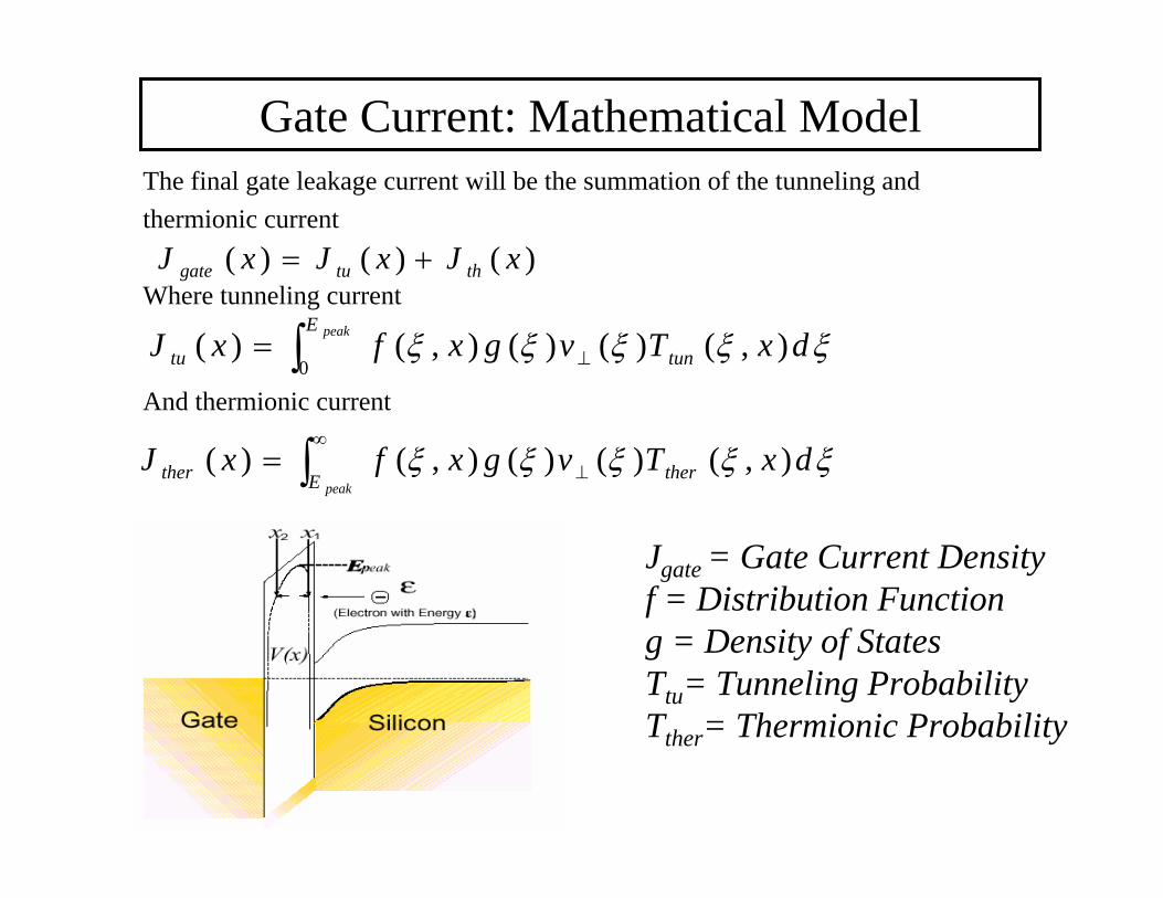
Gate Current: Mathematical ModelThe final gate leakage current will be the summation of the tunneling andthermionic current
Where tunneling current
And thermionic current
)()()( xJxJxJ thtugate +=
ξξξξξ dxTvgxfxJ tun
E
tupeak ),()()(),()(
0 ⊥∫=
ξξξξξ dxTvgxfxJ therEtherpeak
),()()(),()( ⊥
∞
∫=
Jgate = Gate Current Densityf = Distribution Functiong = Density of StatesTtu= Tunneling ProbabilityTther= Thermionic Probability
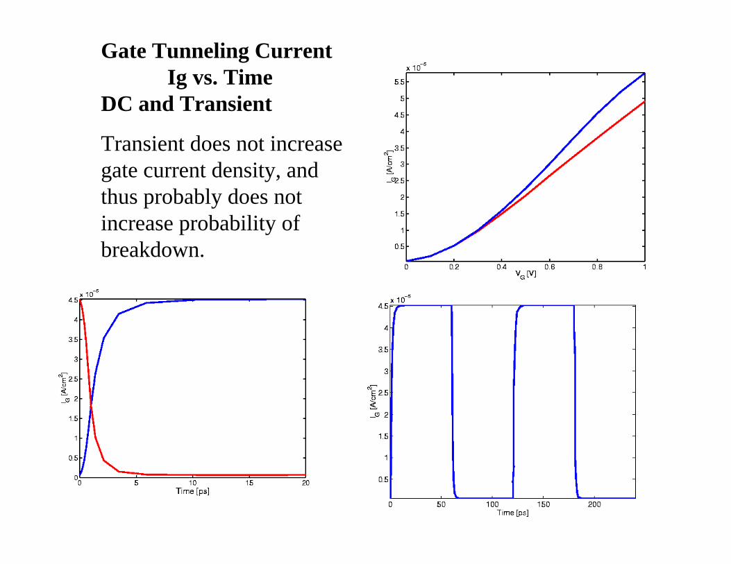
Gate Tunneling Current Ig vs. Time
DC and Transient
Transient does not increase gate current density, and thus probably does not increase probability of breakdown.
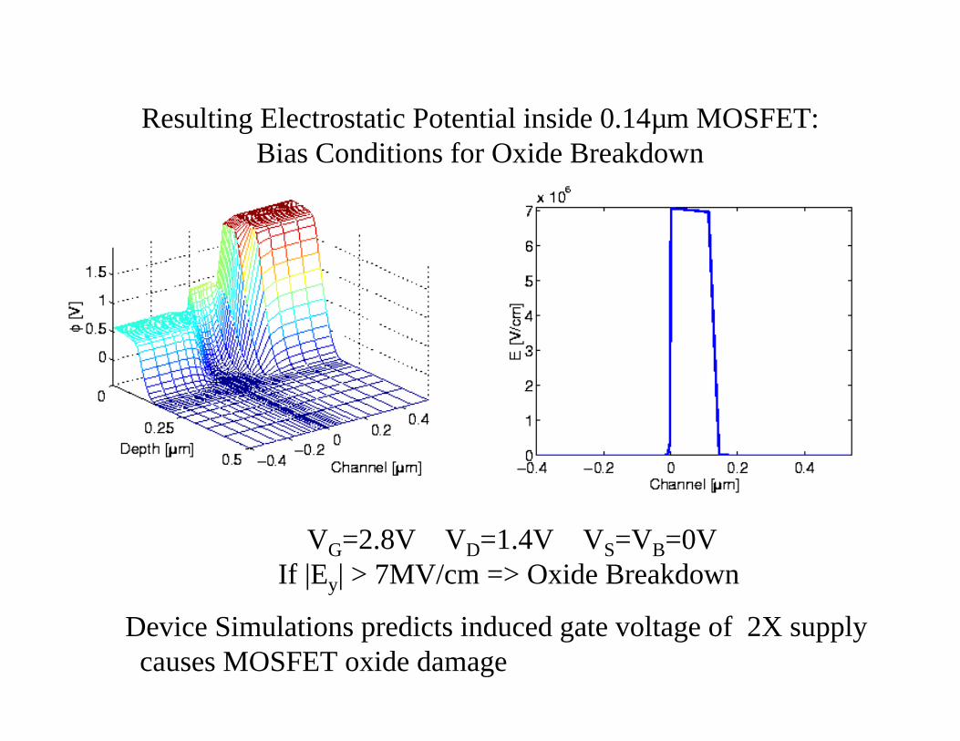
VG=2.8V VD=1.4V VS=VB=0VIf |Ey| > 7MV/cm => Oxide Breakdown
Resulting Electrostatic Potential inside 0.14µm MOSFET: Bias Conditions for Oxide Breakdown
Device Simulations predicts induced gate voltage of 2X supply causes MOSFET oxide damage
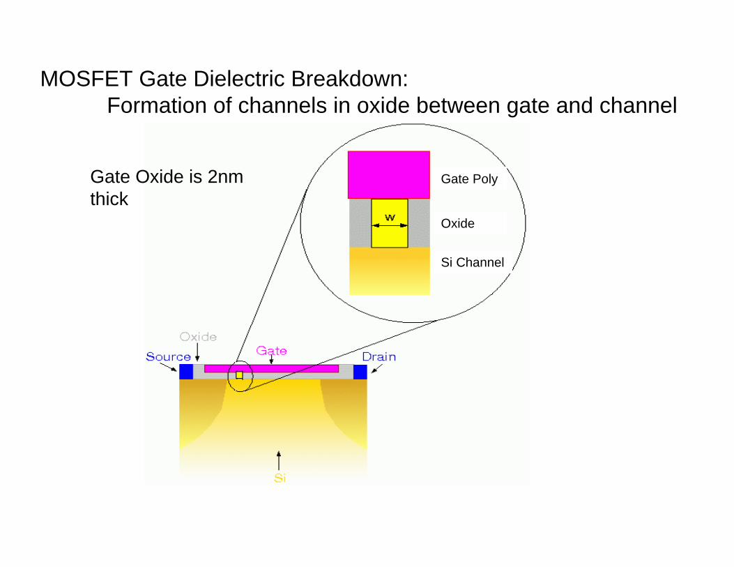
MOSFET Gate Dielectric Breakdown: Formation of channels in oxide between gate and channel
Gate Poly
Oxide
Si Channel
Gate Oxide is 2nm thick
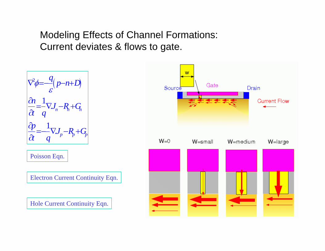
( )2
1 .
1 .
n n n
p p p
q p n D
n J R Gt qp J R Gt q
φε
∇ =− − +
∂= ∇ − +
∂∂=− ∇ − +
∂
Poisson Eqn.
Electron Current Continuity Eqn.
Hole Current Continuity Eqn.
Modeling Effects of Channel Formations: Current deviates & flows to gate.
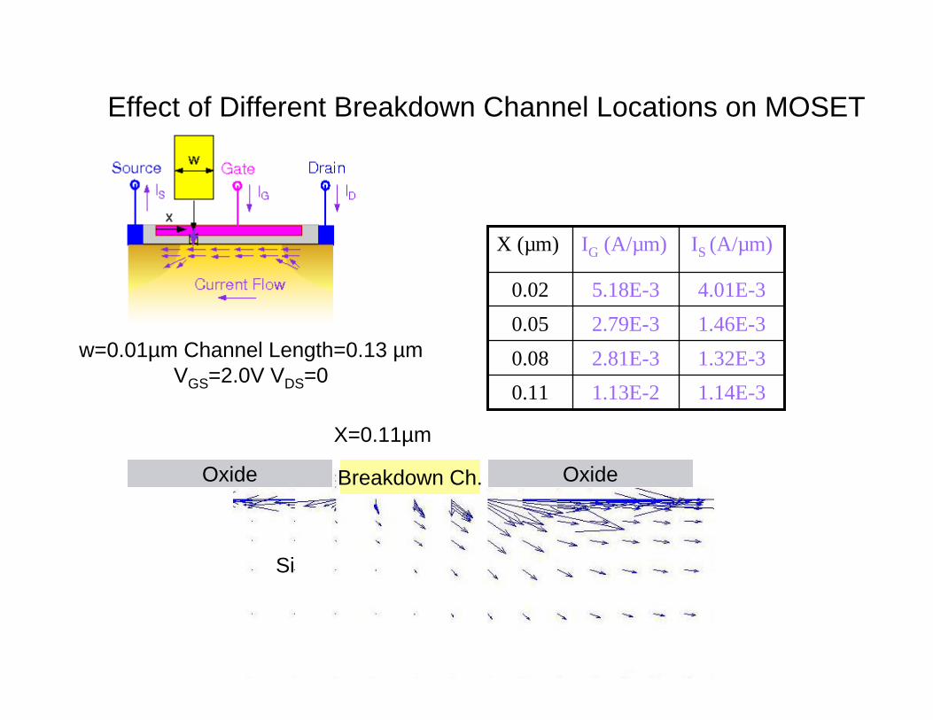
X=0.11µm
w=0.01µm Channel Length=0.13 µm VGS=2.0V VDS=0
1.14E-31.13E-20.111.32E-32.81E-30.081.46E-32.79E-30.054.01E-35.18E-30.02
IS (A/µm)IG (A/µm)X (µm)
Effect of Different Breakdown Channel Locations on MOSET
OxideOxide Breakdown Ch.
Si
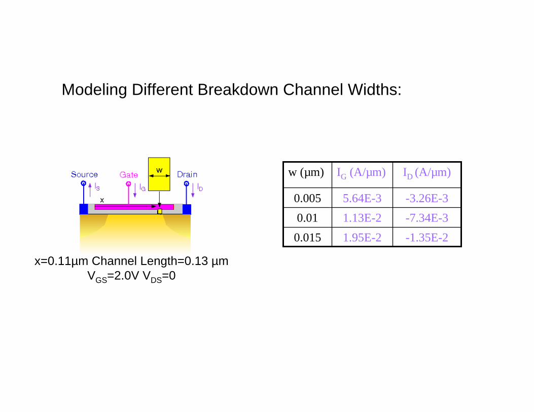
x=0.11µm Channel Length=0.13 µm VGS=2.0V VDS=0
-1.35E-2-7.34E-3-3.26E-3
ID (A/µm)
1.95E-20.0151.13E-20.015.64E-30.005
IG (A/µm)w (µm)
Modeling Different Breakdown Channel Widths:

Differential equation based modeling of EM effects on inverter circuits
Task 2. EM Effects on Gates
• Stage 1: Develop simulation tool.• Stage 2: Use tool to analyze distributed effects of
EM GHz range coupling on fundamental computer chip circuit elements.
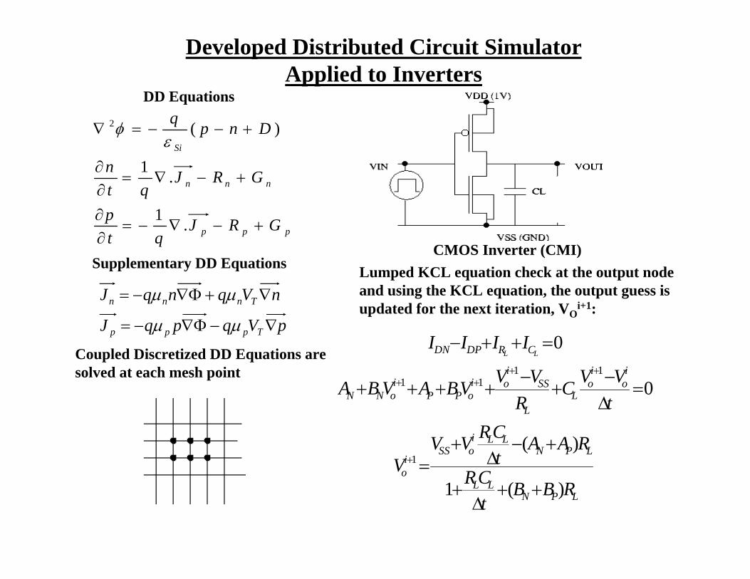
ppp
nnn
Si
GRJqt
p
GRJqt
n
Dnpq
+−∇−=∂∂
+−∇=∂∂
+−−=∇
.1
.1
)(2
εφ
DD Equations
pVqpqJ
nVqnqJ
Tppp
Tnnn
∇−Φ∇−=
∇+Φ∇−=
µµ
µµ
Supplementary DD Equations
Coupled Discretized DD Equations are solved at each mesh point
CMOS Inverter (CMI)
LPNLL
LPNLLi
oSSi
o
io
io
LL
SSi
oioPP
ioNN
CRDPDN
RBBtCR
RAAtCRVV
V
tVVC
RVVVBAVBA
IIIILL
)(1
)(
0
0
1
1111
++∆
+
+−∆
+=
=∆−
+−
++++
=++−
+
++++
Lumped KCL equation check at the output nodeand using the KCL equation, the output guess isupdated for the next iteration, VO
i+1:
Developed Distributed Circuit Simulator Applied to Inverters

L=0.1µm or 0.25µm
Modeling 20GHz, 1V Coupled to 0.1µm & 0.25µm Inverters -Output follows input but with
reduced amplitude in 0.25-Bit errors can still occur in larger device but may be less likely
0.1µm Output 0.25µm Output
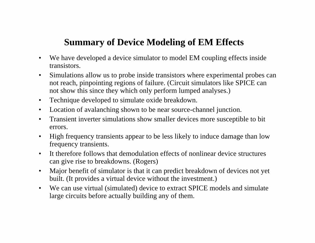
Summary of Device Modeling of EM Effects• We have developed a device simulator to model EM coupling effects inside
transistors.• Simulations allow us to probe inside transistors where experimental probes can
not reach, pinpointing regions of failure. (Circuit simulators like SPICE can not show this since they which only perform lumped analyses.)
• Technique developed to simulate oxide breakdown.• Location of avalanching shown to be near source-channel junction.• Transient inverter simulations show smaller devices more susceptible to bit
errors. • High frequency transients appear to be less likely to induce damage than low
frequency transients.• It therefore follows that demodulation effects of nonlinear device structures
can give rise to breakdowns. (Rogers)• Major benefit of simulator is that it can predict breakdown of devices not yet
built. (It provides a virtual device without the investment.)• We can use virtual (simulated) device to extract SPICE models and simulate
large circuits before actually building any of them.
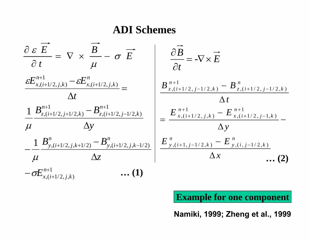
Developed Finite Difference Time Domain Alternating Direction Implicit Method (FDTD-ADI) for Solving Maxwell’s Equations on Chip.
Task 3. Interconnects and Passive Elements
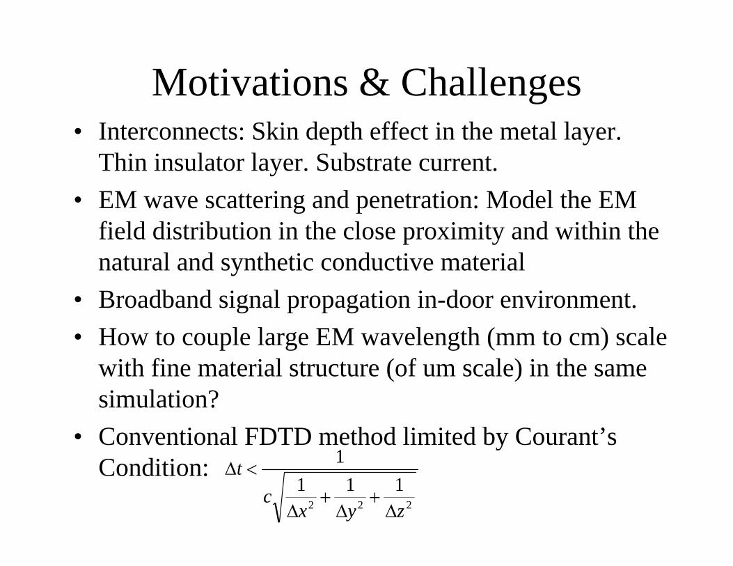
Motivations & Challenges• Interconnects: Skin depth effect in the metal layer.
Thin insulator layer. Substrate current.• EM wave scattering and penetration: Model the EM
field distribution in the close proximity and within the natural and synthetic conductive material
• Broadband signal propagation in-door environment.• How to couple large EM wavelength (mm to cm) scale
with fine material structure (of um scale) in the same simulation?
• Conventional FDTD method limited by Courant’s Condition:
222111
1
zyxc
t
∆+
∆+
∆
<∆
EBtE σ
µε
−×∇=∂
∂
… (2)1
),,2/1(,
)2/1,,2/1(,)2/1,,2/1(,
1),2/1,2/1(,
1),2/1,2/1(,
),,2/1(,1
),,2/1(,
1
1
++
−+++
+−+
+++
+++
−
∆
−−
∆
−
=∆
−
nkjix
nkjiy
nkjiy
nkjiz
nkjiz
nkjix
nkjix
EzBB
yBB
tEE
σµ
µ
εε
ADI Schemes
xEEyEEtBB
nkjiy
nkjiy
nkjix
nkjix
nkjiz
nkjiz
∆
−
−∆
−=
∆
−
−−+
+−+
++
−++
−+
),2/1,(,),2/1,1(,
1),1,2/1(,
1),,2/1(,
),2/1,2/1(,1
),2/1,2/1(,
… (1)
- EtB
×∇=∂∂
Example for one component
Namiki, 1999; Zheng et al., 1999
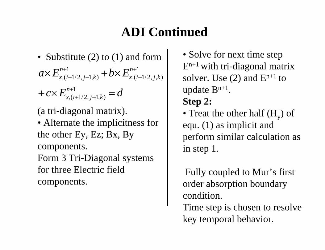
ADI Continued
• Substitute (2) to (1) and form
(a tri-diagonal matrix). • Alternate the implicitness for the other Ey, Ez; Bx, By components.Form 3 Tri-Diagonal systems for three Electric field components.
• Solve for next time step En+1 with tri-diagonal matrix solver. Use (2) and En+1 to update Bn+1.Step 2:• Treat the other half (Hy) of equ. (1) as implicit and perform similar calculation as in step 1.
Fully coupled to Mur’s first order absorption boundary condition.Time step is chosen to resolve key temporal behavior.
dEc
EbEan
kjix
nkjix
nkjix
=×+
×+×+
++
++
+−+
1),1,2/1(,
1),,2/1(,
1),1,2/1(,

Simulating Signal Propagation along Metal-Insulator-Silicon (MIS) Interconnect
x
y
metal
Lossy Silicon Substratez
SiO2Vacuum 500
um
1.8 um
2 um
500um
555 um 555 um6 um
Cross Section of Simulated MIS Structure

Simulation Performance• Non-uniform grid in the cross section; smallest grid
size in the cross section is 0.1 um. Uniform grid = 25 um in the propagation direction.
• Simulation ∆t = 2x10-13 sec. Courant’s limit is ∆t < 0.33×10⁻¹⁵sec
• Simulation time is 3-4 hour on a PC for 1000 step simulation.
• Outer boundary condition: Mur’s first order
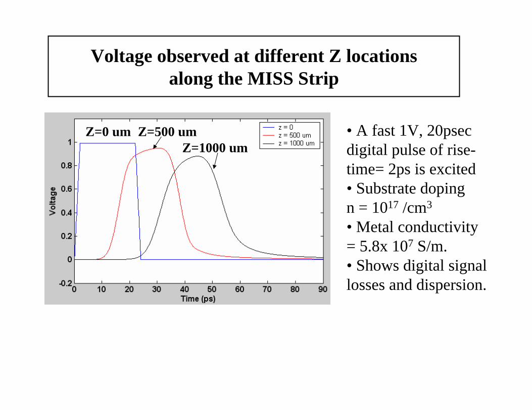
Voltage observed at different Z locations along the MISS Strip
Z=500 umZ=1000 um
Z=0 um • A fast 1V, 20psec digital pulse of rise-time= 2ps is excited• Substrate doping n = 1017 /cm3
• Metal conductivity = 5.8x 10⁷ S/m.• Shows digital signal losses and dispersion.
X (um)
X 10 5
X (um)
X 10 5
SiO2
metal
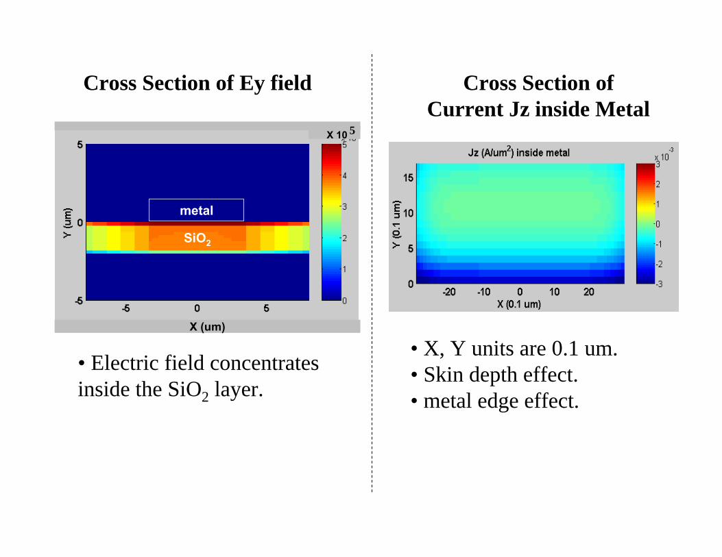
Cross Section of Ey field Cross Section of Current Jz inside Metal
• Electric field concentrates inside the SiO2 layer.
• X, Y units are 0.1 um.• Skin depth effect.• metal edge effect.
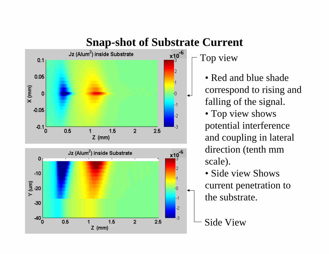
Snap-shot of Substrate Currentx10-6
x10-6x10-6
Top view
Side View
• Red and blue shade correspond to rising and falling of the signal. • Top view shows potential interference and coupling in lateral direction (tenth mm scale). • Side view Shows current penetration to the substrate.

Signal Propagation with Different Substrate Doping
• n1 = 1018 /cm3 (solid)• n2 = 1016 /cm3
(dashed)•At the skin-effect mode, higher substrate doping conforms signal better.
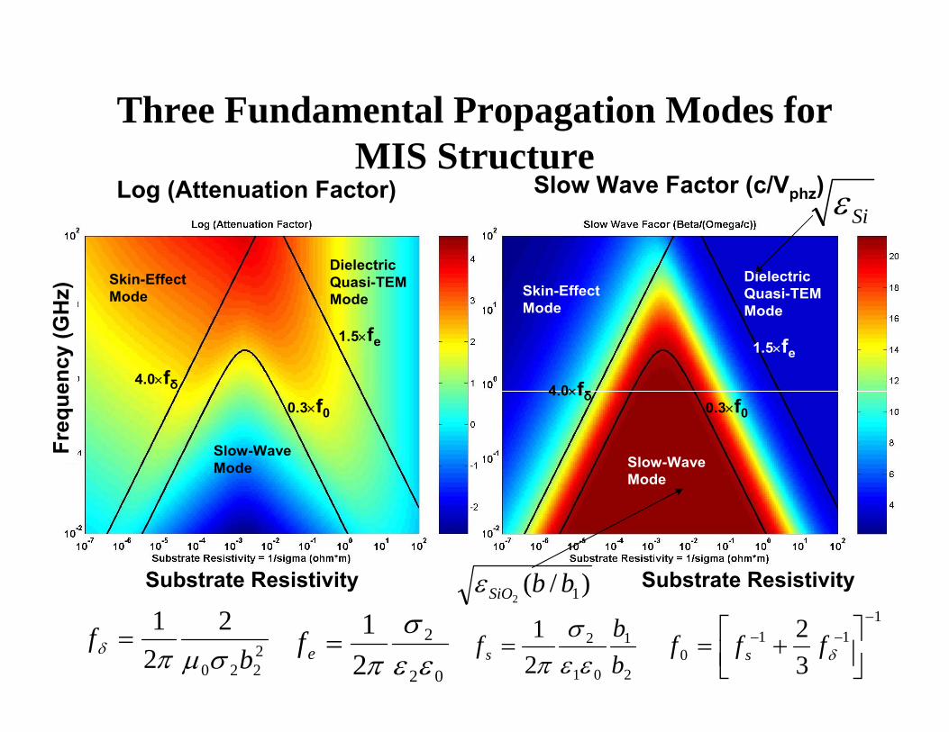
Three Fundamental Propagation Modes for MIS Structure
Skin-Effect Mode
DielectricQuasi-TEM Mode
Slow-Wave Mode
4.0×fδ
1.5×fe
0.3×f0
Skin-Effect Mode
DielectricQuasi-TEM Mode
Slow-Wave Mode
4.0×fδ
1.5×fe
0.3×f0
1.5×fe
4.0×fδ
Skin-Effect Mode
Slow-Wave Mode
DielectricQuasi-TEM Mode
0.3×f0
1.5×fe
4.0×fδ
Skin-Effect Mode
Slow-Wave Mode
DielectricQuasi-TEM Mode
0.3×f0
Log (Attenuation Factor) Slow Wave Factor (c/Vphz)
)/( 12bbSiOε
Siε
2220
221
bf
σµπδ =
Substrate Resistivity Substrate Resistivity
Freq
uenc
y (G
Hz)
02
2
21
εεσ
π=ef
2
1
01
2
21
bbf s εε
σπ
=1
110 3
2 −−−⎥⎦⎤
⎢⎣⎡ += δfff s
500um
500um
1.8 um2 um
x
yz
555 um555 um 6 um
6um
20um
Lossy Silicon Substrate
Activemetal line
SiO2
VacuumPassivemetal line
500um
500um
1.8 um2 um
x
yz
555 um555 um 6 um
6um
20um
Lossy Silicon Substrate
Activemetal line
SiO2
VacuumPassivemetal line
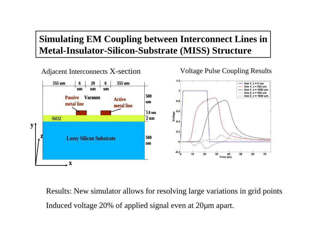
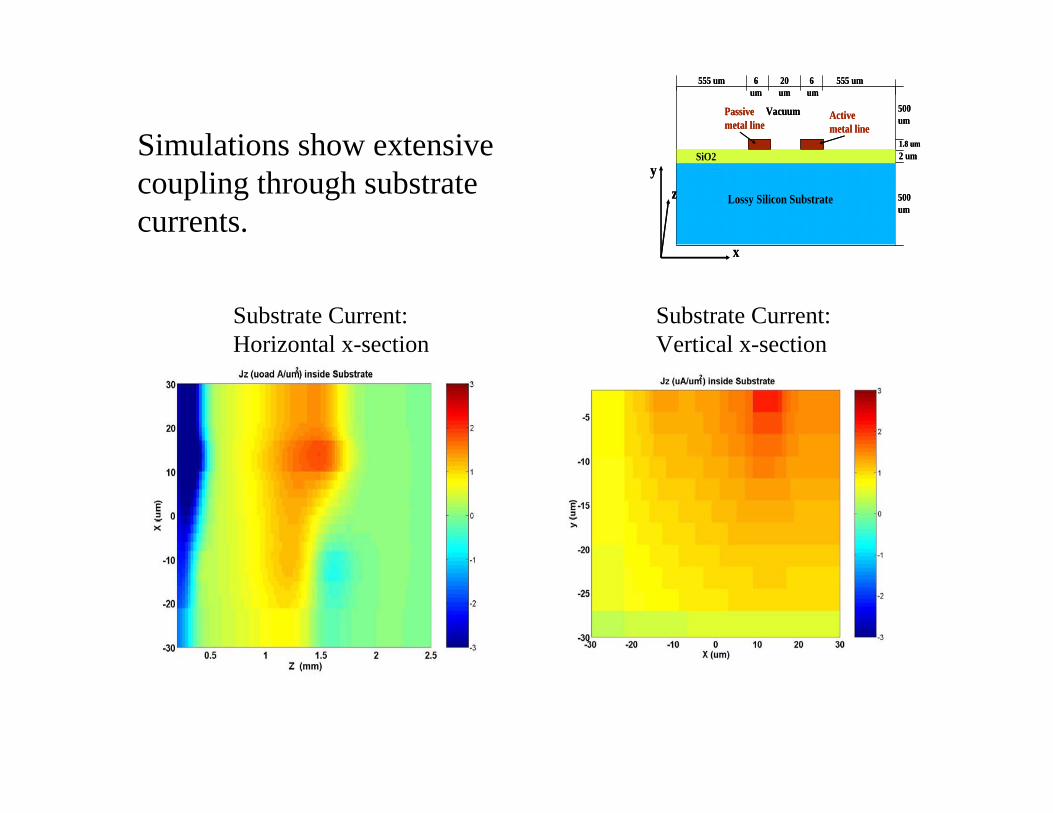
Simulating EM Coupling between Interconnect Lines inMetal-Insulator-Silicon-Substrate (MISS) Structure
Adjacent Interconnects X-section Voltage Pulse Coupling Results
Results: New simulator allows for resolving large variations in grid points
Induced voltage 20% of applied signal even at 20µm apart.
500um
500um
1.8 um2 um
x
yz
555 um555 um 6 um
6um
20um
Lossy Silicon Substrate
Activemetal line
SiO2
VacuumPassivemetal line
500um
500um
1.8 um2 um
x
yz
555 um555 um 6 um
6um
20um
Lossy Silicon Substrate
Activemetal line
SiO2
VacuumPassivemetal line
Simulations show extensive coupling through substrate currents.
Substrate Current: Horizontal x-section
Substrate Current: Vertical x-section
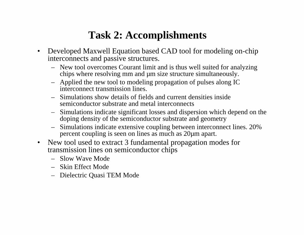
Task 2: Accomplishments• Developed Maxwell Equation based CAD tool for modeling on-chip
interconnects and passive structures.– New tool overcomes Courant limit and is thus well suited for analyzing
chips where resolving mm and µm size structure simultaneously.– Applied the new tool to modeling propagation of pulses along IC
interconnect transmission lines.– Simulations show details of fields and current densities inside
semiconductor substrate and metal interconnects– Simulations indicate significant losses and dispersion which depend on the
doping density of the semiconductor substrate and geometry– Simulations indicate extensive coupling between interconnect lines. 20%
percent coupling is seen on lines as much as 20µm apart.• New tool used to extract 3 fundamental propagation modes for
transmission lines on semiconductor chips– Slow Wave Mode– Skin Effect Mode– Dielectric Quasi TEM Mode
Task 3: EM-Sensitive Passive Components on Semiconductor Chips: Modeling, Testing and
Design• Modern RF circuits often feature on-chip inductors required by
circuit design– Operating frequencies are high enough to make this feasible
• Increasing circuit complexity also creates other inductive components– Long transmission (bus) lines; signal/clock distribution
networks…
Motivation• Investigating parasitic effects
– Vulnerability to external EM coupling– Potential to create on-chip interference
• Radiation• Substrate current
• System-on-a-chip RF circuits require on-chip inductors with high L, small area and high Q– Automated design and speedy evaluation of geometrical
tradeoffs.• On-Chip Inductors are fundamental elements for RF
IC’s.• Different geometries will resonate with different
external RF
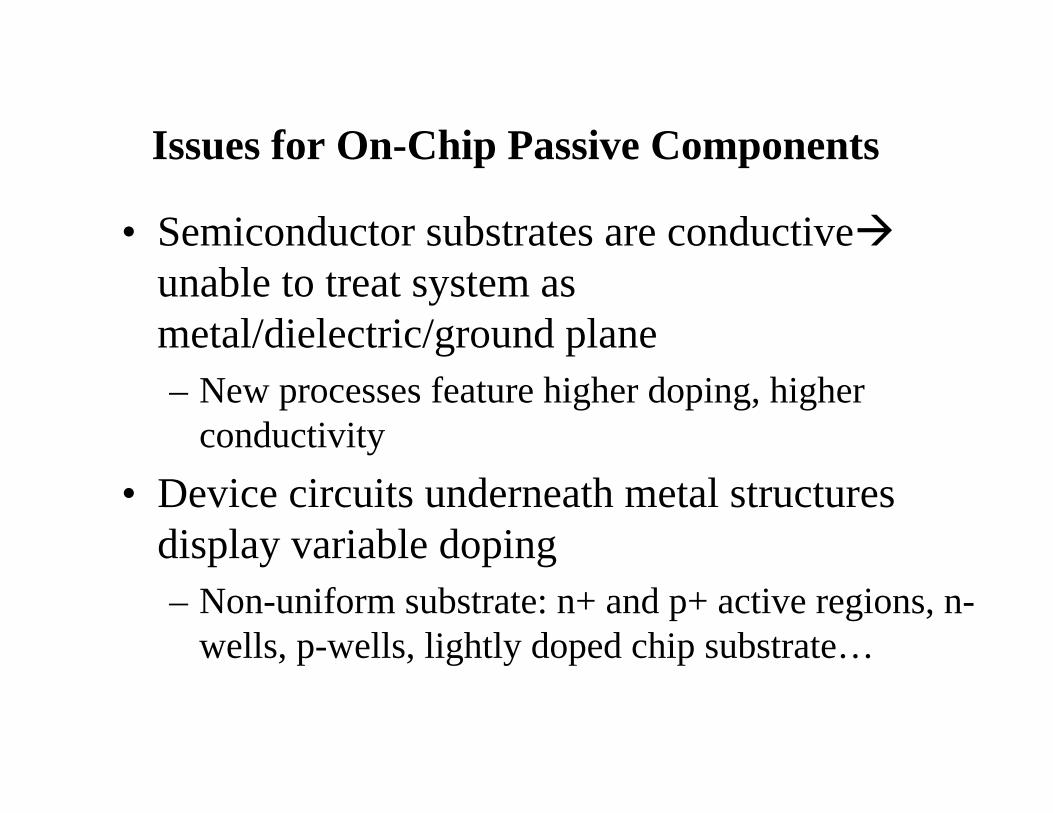
Issues for On-Chip Passive Components
• Semiconductor substrates are conductiveunable to treat system as metal/dielectric/ground plane– New processes feature higher doping, higher
conductivity• Device circuits underneath metal structures
display variable doping– Non-uniform substrate: n+ and p+ active regions, n-
wells, p-wells, lightly doped chip substrate…
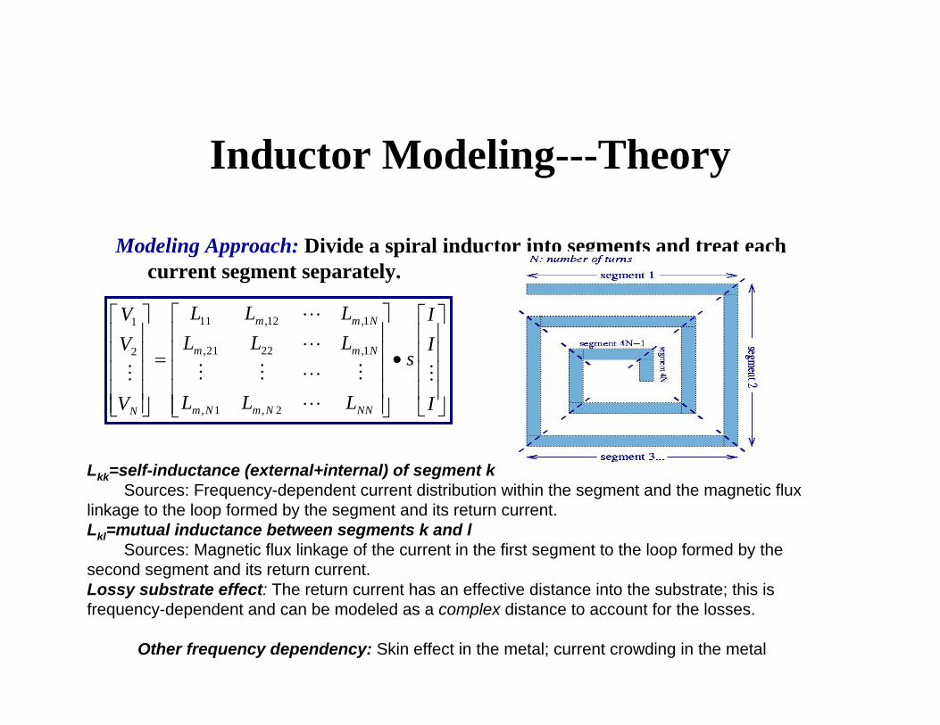
Inductor Modeling---Theory
Modeling Approach: Divide a spiral inductor into segments and treat each current segment separately.
11 ,12 ,11
,21 22 ,12
, 1 , 2
m m N
m m N
m N m N NNN
L L LV IL L LV I
s
L L LV I
⎡ ⎤⎡ ⎤ ⎡ ⎤⎢ ⎥⎢ ⎥ ⎢ ⎥⎢ ⎥⎢ ⎥ ⎢ ⎥= •⎢ ⎥⎢ ⎥ ⎢ ⎥⎢ ⎥⎢ ⎥ ⎢ ⎥
⎢ ⎥ ⎢ ⎥ ⎣ ⎦⎣ ⎦ ⎣ ⎦
Lkk=self-inductance (external+internal) of segment kSources: Frequency-dependent current distribution within the segment and the magnetic flux
linkage to the loop formed by the segment and its return current. Lkl=mutual inductance between segments k and l
Sources: Magnetic flux linkage of the current in the first segment to the loop formed by the second segment and its return current.Lossy substrate effect: The return current has an effective distance into the substrate; this is frequency-dependent and can be modeled as a complex distance to account for the losses.
Other frequency dependency: Skin effect in the metal; current crowding in the metal

Mutual Inductance
,
14
i j
i i j j
j
c c j i ji ja b a b
i ijm ij
j ja
J d l d ld a d a
a RL
J d a
µπ
•
=∫ ∫ ∫ ∫
∫
Mutual inductance: The magnetic flux created by the current on one loop linking to the area of other loop
ijij
j
LIΨ
=
Calculate Ψ from the magnetic vector potential and I from the current distribution; the mutual inductance between two current segments is then
Frequency dependency: The signal current of a current segment and its image current both induce voltages on the “target” current segment; the distribution of the image current varies with frequency on a semiconductor substrate.
xpx qx
2pW
−2
pW2
qW−
2qW
( )qxJ
( )qxJ−
'qqh
yz
Virtual Ground Plane
qp
'q (image)
1py
2py
1qy
2qypqh
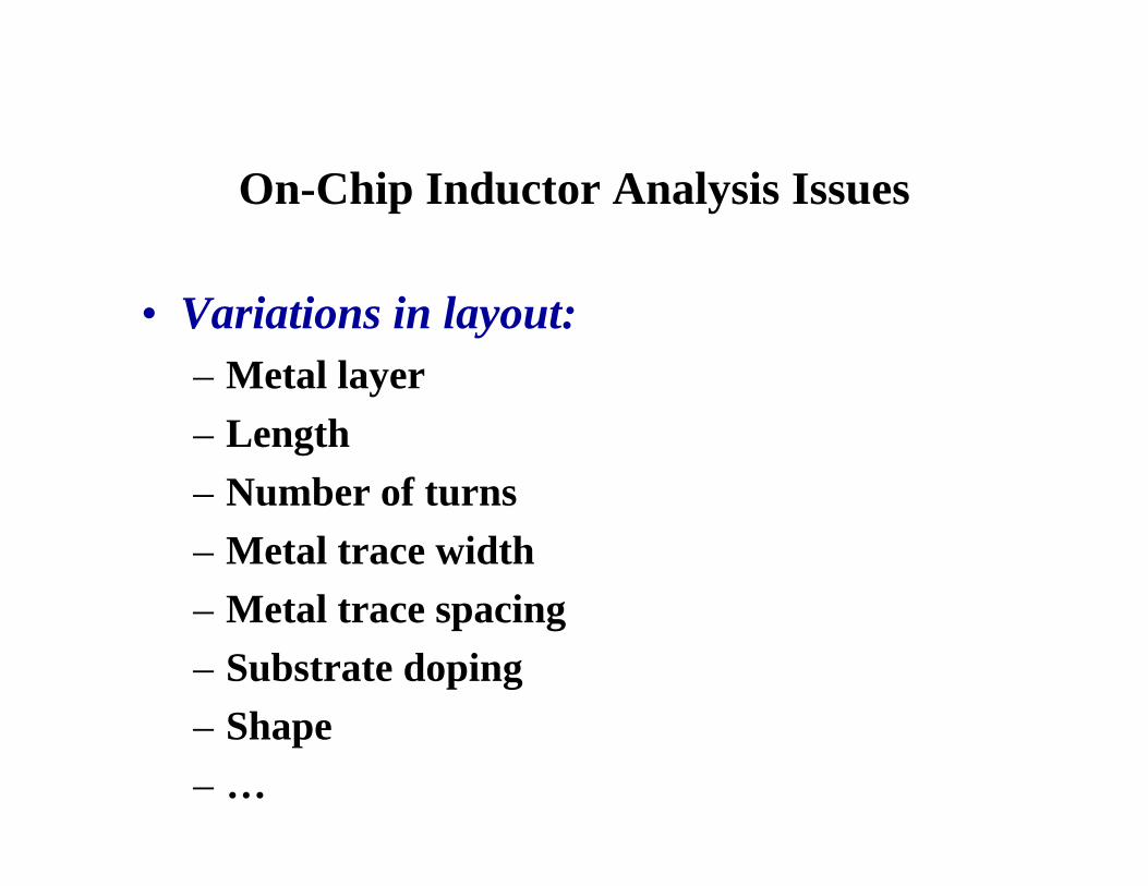
On-Chip Inductor Analysis Issues
• Variations in layout:– Metal layer– Length– Number of turns– Metal trace width– Metal trace spacing– Substrate doping– Shape– …
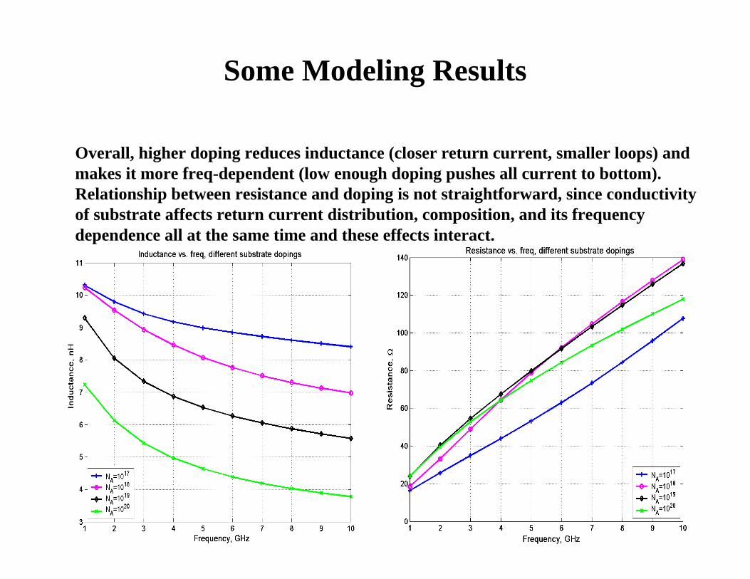
Some Modeling ResultsSubstrate Doping VariationOverall, higher doping reduces inductance (closer return current, smaller loops) and makes it more freq-dependent (low enough doping pushes all current to bottom). Relationship between resistance and doping is not straightforward, since conductivity of substrate affects return current distribution, composition, and its frequency dependence all at the same time and these effects interact.
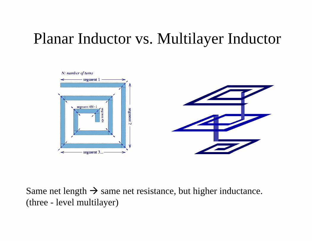
Planar Inductor vs. Multilayer Inductor
Same net length same net resistance, but higher inductance.(three - level multilayer)
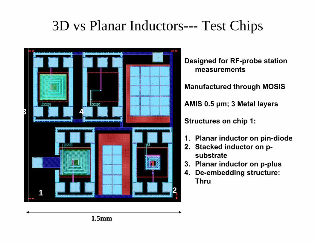
3D vs Planar Inductors--- Test Chips
Designed for RF-probe station measurements
Manufactured through MOSIS
AMIS 0.5 µm; 3 Metal layers
Structures on chip 1:
1. Planar inductor on pin-diode 2. Stacked inductor on p-
substrate3. Planar inductor on p-plus4. De-embedding structure:
Thru1 2
3 4
1.5mm
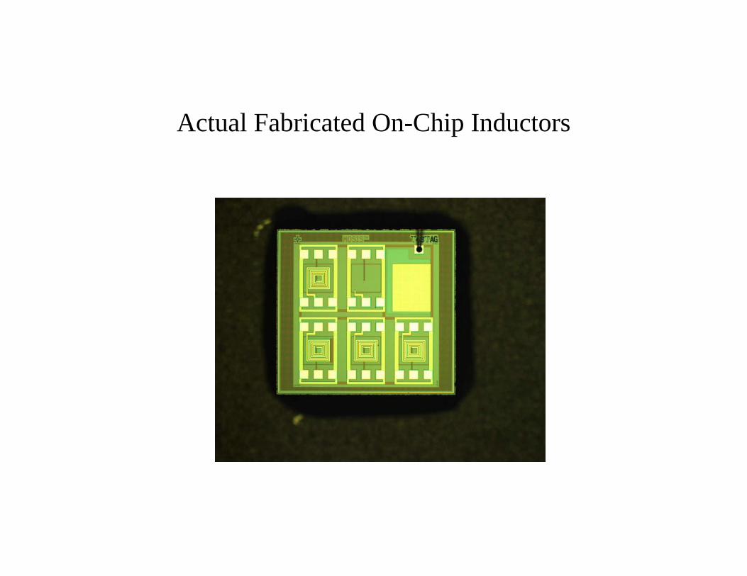
Actual Fabricated On-Chip Inductors

Test Chip: Investigating Micro GeometryPlanar vs Stacked Inductors
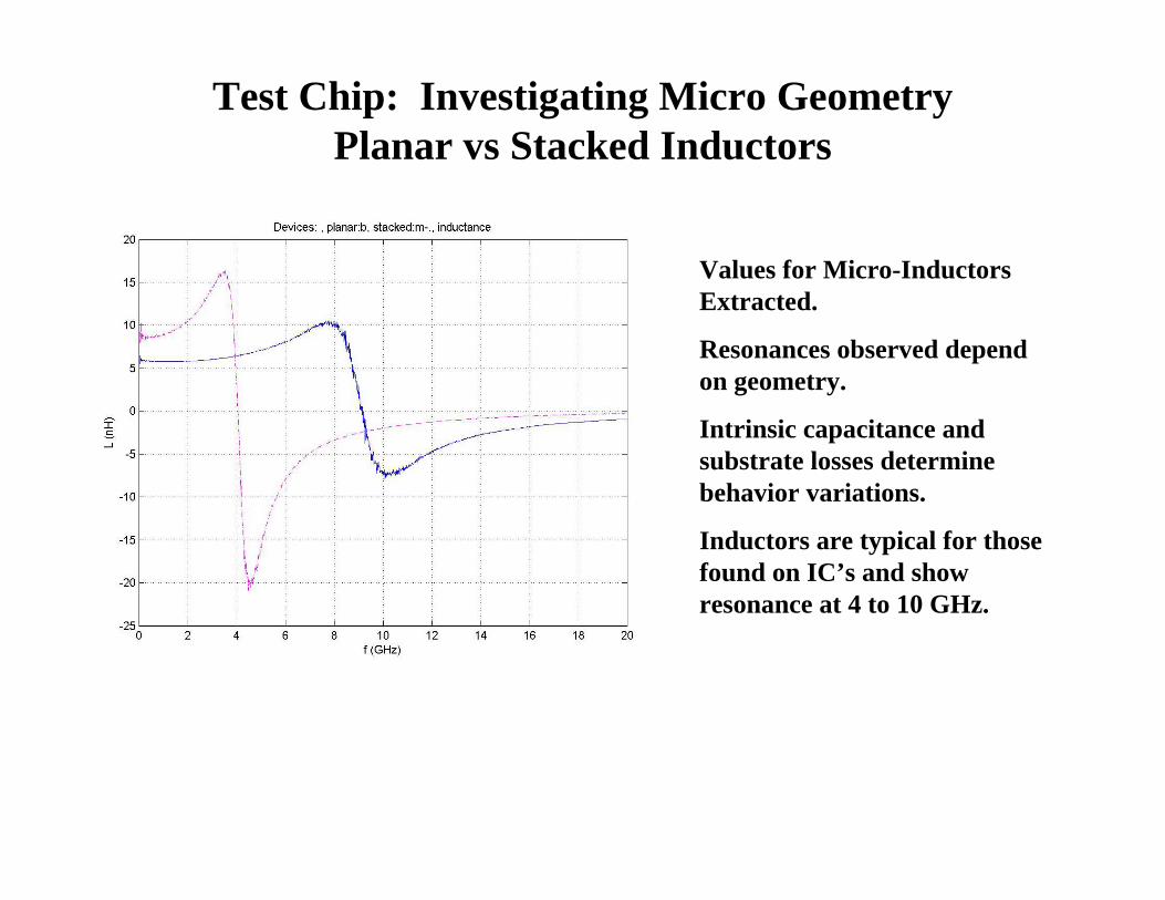
Test Chip: Investigating Micro GeometryPlanar vs Stacked Inductors
Values for Micro-Inductors Extracted.
Resonances observed depend on geometry.
Intrinsic capacitance and substrate losses determine behavior variations.
Inductors are typical for those found on IC’s and show resonance at 4 to 10 GHz.

Test Chip: Investigating Micro InductorsEffect of Silicon Substrate Doping
Designed for RF-probe station measurements
Manufactured through MOSIS
AMIS 0.5 µm; 3 Metal layers
Structures on chip 1:
1. Planar inductor on grounded poly
2. Planar inductor on n-well3. Planar inductor on p-
substrate4. Planar inductor on n-plus5. De-embedding structure:
Open1 2 3
4 5

Test Chip: Investigating Micro InductorsEffect of Silicon Substrate Doping
Measurements show resonance for much higher doped substrate occurs at lower frequency.
Indicates higher intrinsic capacitance for more highly doped system.
Future Work• Continue modeling of oxide breakdown in nanoscale
MOSFETs.• Extend MOSFET oxide breakdown modeling to transient
case.• Continue modeling of on-chip interconnects using ADI
code.• Investigate effect of doping and geometry on how bus lines
couple to external EM.• Continue experiments and modeling on on-chip passive
elements.• Extend theory for calculating inductance to include intrinsic
capacitance effects as well.

Publications• C.K. Huang and N. Goldsman, Non-equilibrium modeling of tunneling gate currents in nanoscale
MOSFETs, Solid State Electronics, vol. 47: pp. 713-720, 2003.• A. Akturk, N. Goldsman and G. Metze, ``Faster CMOS Inverter Switching Obtained withChannel
Engineered Asymmetrical Halo Implanted MOSFETs, Solid State Electronics, vol. 47, pp.~185--192, 2003.
• X. Shao, N. Goldsman, O. M. Ramahi, P. N. Guzdar, A New Method for Simulation of On-Chip Interconnects and Substrate Currents with 3D Alternating-Direction-Implicit (ADI) Maxwell Equation Solver. International Conference on Simulation of Semiconductor Processes and Devices, pp. 315-318, 2003.
• X. Shao, N. Goldsman, and O. M Ramahi, The Alternating-Direction Implicit Finite-Difference Time-Domain (ADI-FDTD) Method and its Application to Simulation of Scattering from Highly Conductive Material, IEEE International Antennas and Propagation Symposium and USNC/CNC/URSI North American Radio Science Meeting: URSI, Digest, p. 358, 2003.
• Y. Bai, Z. Dilli, N. Goldsman and G. Metze, Frequency-Dependent Modeling of On-Chip Inductors on Lossy Substrate, International Semiconductor Device Research Symposium, pp. 292-293, 2003.
• 6. X. Shao, N. Goldsman, O. M. Ramahi,and P. N. Guzdar, Modeling RF Effects in Integrated Circuits with a New 3D Alternating-Direction-Implicit Maxwell Equation Solver, International Semiconductor Device Research Symposium, pp. 532-533, 2003.


![Semiconductor Devices [Kanaan Kano]](https://static.fdocuments.in/doc/165x107/55cf931a550346f57b9bb747/semiconductor-devices-kanaan-kano.jpg)