Electronics in High Energy Physics Introduction to Electronics in HEP Field Programmable Gate Arrays...
36
Electronics in High Energy Physics Introduction to Electronics in HEP Field Programmable Gate Arrays Part 1 based on the lecture of S.Haas
-
Upload
lee-hoover -
Category
Documents
-
view
216 -
download
2
Transcript of Electronics in High Energy Physics Introduction to Electronics in HEP Field Programmable Gate Arrays...

Electronics in High Energy PhysicsIntroduction to Electronics in HEP
Field Programmable Gate ArraysPart 1
based on the lecture of S.Haas

2
Part 2• VHDL
– Introduction– Examples
• Design Flow– Entry Methods– Simulation– Synthesis– Place & Route
• IP Cores• CERN Tools & Support
Part 1• Programmable Logic• CPLD• FPGA
– Architecture– Examples– Features– Vendors and Devices
coffee break
Outline

Programmable Logic

4
Programmable Logic
• Programmable digital integrated circuit• Standard off-the-shelf parts• Desired functionality is implemented by configuring
on-chip logic blocks and interconnections• Advantages (compared to an ASIC):
– Low development costs– Short development cycle– Device can (usually) be reprogrammed
• Types of programmable logic:– Complex PLDs (CPLD)– Field programmable Gate Arrays (FPGA)

CPLDArchitecture and Examples

6
PLD - Sum of Products
A B C
CBACBAf 1
CBABAf 2
AND plane
Programmable AND array followed by fixed fan-in OR gates
Programmable switch or fuse

7
PLD - Macrocell
Can implement combinational or sequential logic
A B C
Flip-flop
SelectEnable
D Q
Clock
AND plane
MUX
1f

8
CPLD Structure
Integration of several PLD blocks with a programmable interconnect on a single chip
PLDBlockPLD
BlockPLD
BlockPLD
Block
Interconnection MatrixInterconnection Matrix
I/O B
lock
I/O B
lock
I/O B
lock
I/O B
lock
PLDBlockPLD
BlockPLD
BlockPLD
Block
I/O B
lock
I/O B
lock
I/O B
lock
I/O B
lock
• • •
Interconnection MatrixInterconnection Matrix
• • •
• • •
• • •
9
CPLD Example - Altera MAX7000
EPM7000 Series Block Diagram
10
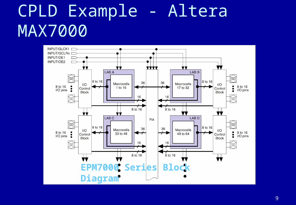
CPLD Example - Altera MAX7000
EPM7000 Series Device Macrocell

FPGA Architecture
12
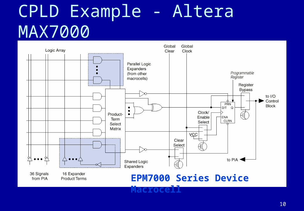
FPGA - Generic Structure
FPGA building blocks:• Programmable logic blocks
Implement combinatorial and sequential logic
• Programmable interconnectWires to connect inputs and outputs to logic blocks
• Programmable I/O blocks Special logic blocks at the periphery of device for external connections
I/O
I/O
Logic block Interconnection switches
I/O
I/O

13
Other FPGA Building Blocks
• Clock distribution
• Embedded memory blocks
• Special purpose blocks:– DSP blocks:
• Hardware multipliers, adders and registers
– Embedded microprocessors/microcontrollers– High-speed serial transceivers
14
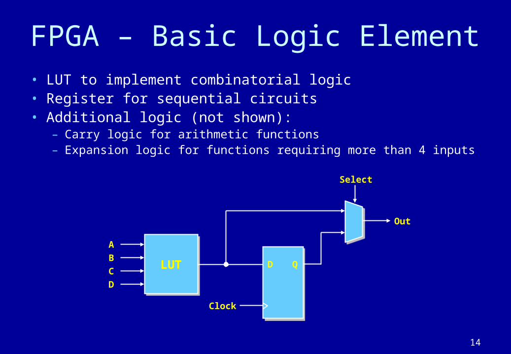
FPGA – Basic Logic Element• LUT to implement combinatorial logic• Register for sequential circuits• Additional logic (not shown):
– Carry logic for arithmetic functions– Expansion logic for functions requiring more than 4 inputs
LUTLUT
Out
Select
D Q
A
B
C
D
Clock

15
Look-Up Tables (LUT)• Look-up table with N-inputs can be used to implement any
combinatorial function of N inputs• LUT is programmed with the truth-table
LUTLUT
ABCD
Z
A
B
C
D
Z
Truth-table Gate implementation
LUT implementation

16
LUT Implementation
• Example: 3-input LUT• Based on multiplexers
(pass transistors)• LUT entries stored in
configuration memory cells
0/10/1
0/10/1
0/10/1
0/10/1
0/10/1
0/10/1
0/10/1
0/10/1
X1X2
X3
F
Configuration memorycells

17
Programmable Interconnect
• Interconnect hierarchy (not shown)– Fast local interconnect– Horizontal and vertical lines of various lengths
LELE
LELE
LELE
LELE
LELE
LELE
SwitchMatrix
Switch Matrix

18
Switch Matrix Operation
• 6 pass transistors per switch matrix interconnect point
• Pass transistors act as programmable switches
• Pass transistor gates are driven by configuration memory cells
After ProgrammingBefore Programming

19
Special Features
• Clock management– PLL,DLL– Eliminate clock skew between external clock input
and on-chip clock– Low-skew global clock distribution network
• Support for various interface standards
• High-speed serial I/Os
• Embedded processor cores
• DSP blocks

20
Configuration Storage Elements• Static Random Access Memory (SRAM)
– each switch is a pass transistor controlled by the state of an SRAM bit– FPGA needs to be configured at power-on
• Flash Erasable Programmable ROM (Flash)– each switch is a floating-gate transistor that can be turned off by
injecting charge onto its gate. FPGA itself holds the program– reprogrammable, even in-circuit
• Fusible Links (“Antifuse”)– Forms a forms a low resistance path when electrically programmed – one-time programmable in special programming machine – radiation tolerant

Example: Altera Stratix Series

22
Floorplan

23
Logic Element

24
Logic Array Block (LAB)
• LAB regroups 10 logic elements with a fast local interconnect
• Interconnect structure– Direct link between LABs
and adjacent blocks– Row interconnects
• 4, 8, and 24 blocks left or right
– Column interconnects• 4, 8, and 16 blocks up or
down
25
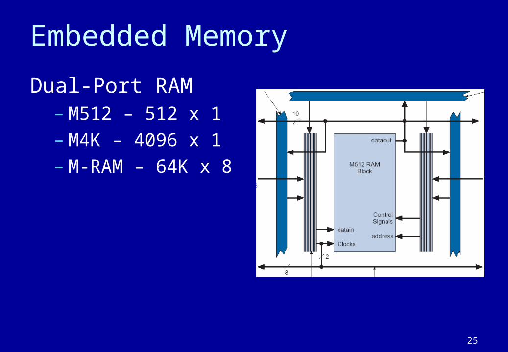
Embedded Memory
Dual-Port RAM– M512 – 512 x 1– M4K – 4096 x 1– M-RAM – 64K x 8

Example: Xilinx Virtex-II Pro

27
Virtex II Pro Floorplan
• 1 to 4 PowerPCs• 4 to 16 multi-gigabit
transceivers• 12 to 216 multipliers• 3,000 to 50,000 logic
cells• 200k to 4M bits RAM• 204 to 852 I/Os L
og
ic
cells
Up to 16 serial transceivers• 622 Mbps to 3.125 Gbps622 Mbps to 3.125 Gbps
PowerPCs

28
Logic Slice Architecture
• Two 4-input LUT, can also be used as:– 16-bit synchronous RAM– 16-bit shift register
• Two flip-flops/latches• Carry logic for arithmetic
circuits (e.g. adder)• Fast width expansion logic
– Implement logic functions with more than 4 inputs

29
Configurable Logic Block (CLB)
• CLB regroups 4 logic slices
• Fast connection to neighbors
• Connections for carry logic and shift register mode
30
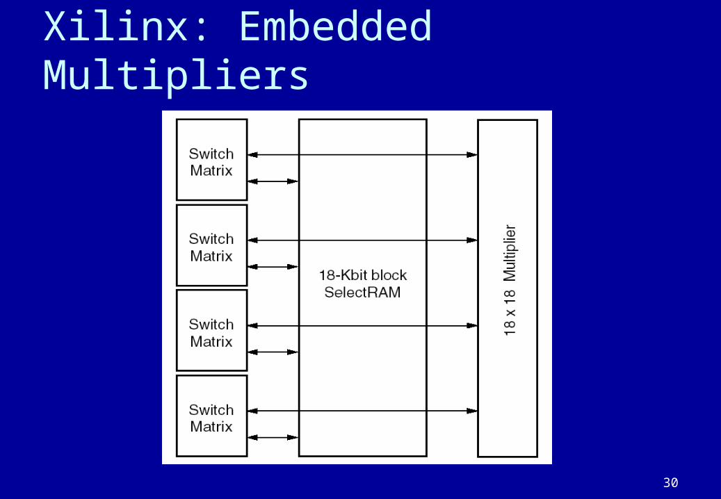
Xilinx: Embedded Multipliers
31
Altera: Embedded DSP Blocks
• Two DSP Block columns per device
• Number varies by height of column
• Can implement:– Eight 9x9 multipliers– Four 18x18 multipliers– One 36x36 multiplier
• Contains adder/subtractor/accumulator
• Registered inputs can become shift register

32
Altera: Embedded DSP Block

33
3.125 Gb/s per pair
32b @ 78 MHz
32b @ 78 MHz
Virtex-II Pro Virtex-II Pro
Xilinx: Rocket I/O
Virtex 4: 11.1 Gbps !!!

34
FPGA Vendors & Device Families• Xilinx
– Virtex-II/Virtex-4: Feature-packed high-performance SRAM-based FPGA
– Spartan 3: low-cost feature reduced version
– CoolRunner: CPLDs• Altera
– Stratix/Stratix-II• High-performance SRAM-
based FPGAs– Cyclone/Cyclone-II
• Low-cost feature reduced version for cost-critical applications
– MAX3000/7000 CPLDs– MAX-II: Flash-based FPGA
• Actel– Anti-fuse based FPGAs
• Radiation tolerant– Flash-based FPGAs
• Lattice– Flash-based FPGAs– CPLDs (EEPROM)
• QuickLogic– ViaLink-based FPGAs

35
State of the Art in FPGAs• 90 nm process on 300 mm wafers
– Lower cost per function (LUT + register)– Smaller and faster transistors: Higher speed
• System speed up to 500 MHz– Mainly through smart interconnects, clock management, dedicated
circuits, flexible I/O. – Integrated transceivers running at 10 Gigabits/sec
• More Logic and Better Features:– >100,000 LUTs & flip-flops– >200 embedded RAMs, and same number 18 x 18 multipliers
• 1156 pins (balls) with >800 GP I/O– 50 I/O standards, incl. LVDS with internal termination
• 16 low-skew global clock lines– Multiple clock management circuits
• On-chip microprocessor(s) and multi-Gbps transceivers
36
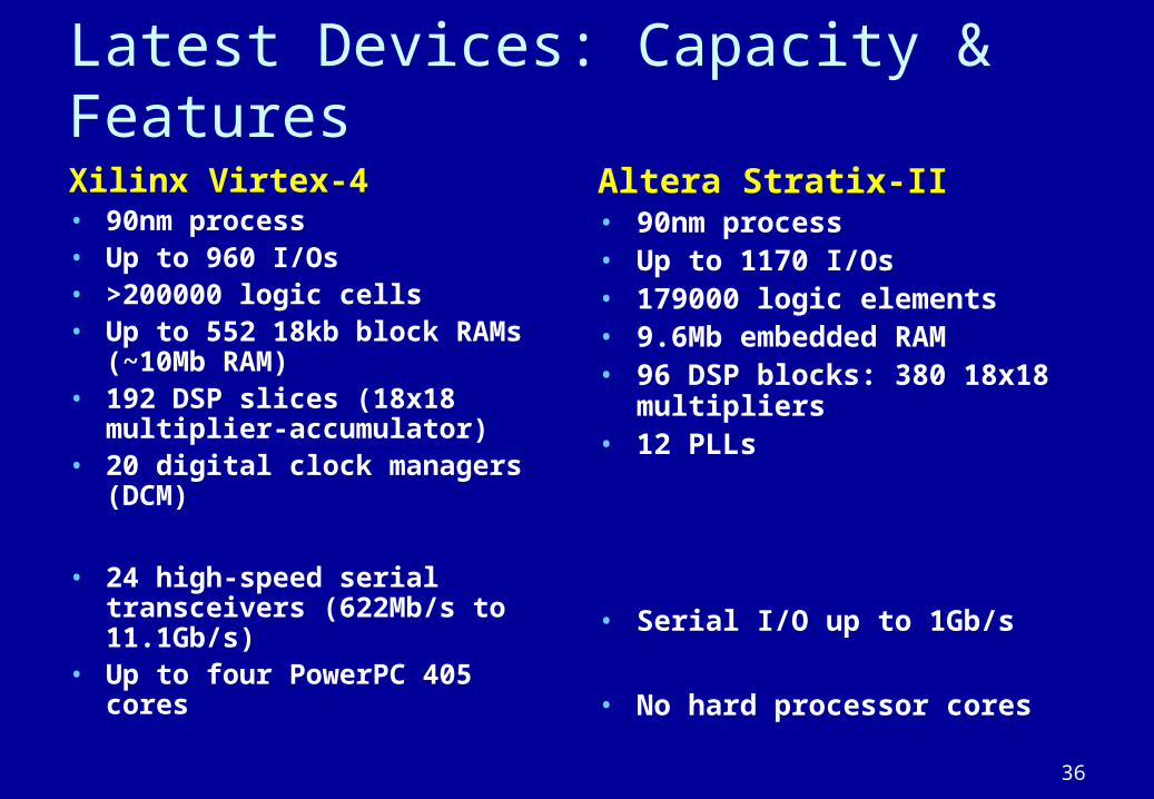
Latest Devices: Capacity & Features
Xilinx Virtex-4• 90nm process• Up to 960 I/Os• >200000 logic cells• Up to 552 18kb block RAMs
(~10Mb RAM)• 192 DSP slices (18x18
multiplier-accumulator)• 20 digital clock managers
(DCM)
• 24 high-speed serial transceivers (622Mb/s to 11.1Gb/s)
• Up to four PowerPC 405 cores
Altera Stratix-II• 90nm process• Up to 1170 I/Os• 179000 logic elements• 9.6Mb embedded RAM• 96 DSP blocks: 380 18x18
multipliers• 12 PLLs
• Serial I/O up to 1Gb/s
• No hard processor cores