Electronic transport, field effect and doping in … · monolayer thin film ... Field effect...
173
Electronic transport, field effect and doping in pentacene nanorods and monolayer thin film prepared by combination of nano-fabrication and self-assembly. Inauguraldissertation zur Erlangung der W¨ urde eines Doktors der Philosophie vorgelegt der Philosophisch-Naturwissenschaftlichen Fakult¨ at der Universit¨ at Basel von Claudio Vanoni aus Aurigeno, Tessin Villigen, 2008
Transcript of Electronic transport, field effect and doping in … · monolayer thin film ... Field effect...

Electronic transport, field effect
and doping
in pentacene nanorods and
monolayer thin film
prepared by combination of
nano-fabrication and self-assembly.
Inauguraldissertation
zurErlangung der Wurde eines Doktors der Philosophie
vorgelegt derPhilosophisch-Naturwissenschaftlichen Fakultat
der Universitat Basel
von
Claudio Vanoni
aus Aurigeno, Tessin
Villigen, 2008

Genehmigt von der Philosophisch-Naturwissenschaftlichen Fakultatauf Antrag von
Prof. Dr. Ch. SchonenbergerDr. T. A. JungDr. W. Riess
Basel, den 19. September 2006
Prof. Dr. Hans-Peter HauriDekan

Abstract
The transport in organic semiconductors is investigated on the na-nometer scale. Field effect transistor with device-active layers in themonolayer (ML) range are characterized in-situ right after the con-trolled deposition of pentacene. By using a bottom contact geometry,the thickness of the channel is varied in several steps and the thinfilm transistors (TFTs) are characterized after each additional depo-sition. The mobility is found to saturate at a channel thickness of3-4 ML. This allows for the operation of 2 ML TFT, where the effectof dopant molecules deposited on top of the channel is studied. Flu-orinated tetracyanoquinodimethane (F4TCNQ) is found to increasethe charge carrier concentration by a charge transfer process withpentacene without degradation of the mobility. For a separation ofcontact effects from bulk effects, TFTs with channel length between20 µm and 200 µm have been processed in parallel. The contact resis-tance Rc and the contact free mobility µcf have been extracted andanalyzed by the transmission line method (TLM).
In temperature dependent studies, an approximately linear log(µ)vs. 1/T relation describes the experimental results. The fit is slightlybetter for the undoped TFT compared to the doped TFT. This is con-sistent with the accepted theoretical models based on a disordered
3

ABSTRACT
Gaussian density of states (DOS). In fact, the experimental determi-nation of the DOS in doped TFTs shows an additional broad peakat 0.14 eV above the HOMO edge caused by the dopant molecules.
A second pronounced effect of doping is the reduction of theRc by a factor 20 between the gold electrode and pentacene. Thegate field dependent decrease of Rc in undoped TFTs is related toa lowering of the Schottky barrier at the interface. In doped TFTs,the opposite effect is observed. This demonstrates the influence ofthe dopant molecules on the interface barrier. The injection pro-cess determining Rc is found to change from a thermionic emissionmechanism to a tunneling regime.
For the investigation of the injection properties at the interface,a new manufacturing method to produce metallic nanojunction ispresented. In combination with a self-assembly process leading topentacene rod-like islands connecting the two electrodes right throughtheir growth, the transport in the 10-nm scale is investigated. At thisscale length, the current-voltage (I-V) characteristics of pentacene ischanging from rectifying Schottky-like behavior to fully linear behav-ior upon F4TCNQ doping. Variable temperature investigations showthat the conduction in the doped pentacene nanojunction is ther-mally activated, with an activation energy very close to the energyposition of the dopant induced peak in the DOS and to the thermalactivation energy of Rc.
keywords:
organic semiconductor, pentacene, field effect, monolayer, mobility,density of states (DOS), transport mechanism, nanoscale transport,nanojuncton, electromigration, nanorods, injection, contact resistance,metal-organic interface, Schottky barrier, doping, thermally assistedtunneling, gate filed modulation, in-situ doping, charge transfer.
4

Contents
Abstract 3
1 Introduction and motivation 9
2 Outline 15
3 Fabrication and characterization of nanojunctions 193.1 Manufacturing process . . . . . . . . . . . . . . . . . . 203.2 Batch process . . . . . . . . . . . . . . . . . . . . . . . 223.3 In-situ control of the nanojunction formation . . . . . 253.4 Concerns on electrical stability . . . . . . . . . . . . . 323.5 Concerns on chemical stability . . . . . . . . . . . . . 37
4 Self-assembly and growth of pentacene thin film 414.1 Principle of self-assembly . . . . . . . . . . . . . . . . 414.2 Pentacene: model for ordered organic semiconductors 45
5
CONTENTS
4.3 Physical vapor deposition of pentacene . . . . . . . . . 464.4 Structural Characterization . . . . . . . . . . . . . . . 49
4.4.1 Methods: AFM, SEM and XRD . . . . . . . . 494.4.2 Pentacene on oxide surface . . . . . . . . . . . 504.4.3 Pentacene on metal surfaces . . . . . . . . . . . 55
5 Electrical transport through self-assembled pentacenenanorods 635.1 Contacting pentacene nanorods by a metallic nano-
junction . . . . . . . . . . . . . . . . . . . . . . . . . . 645.2 Current-voltage measurements of undoped and doped
nanorods . . . . . . . . . . . . . . . . . . . . . . . . . 645.3 Temperature dependence of the conductivity . . . . . 70
5.3.1 Experimetal setup . . . . . . . . . . . . . . . . 705.3.2 Results on doped pentacene . . . . . . . . . . . 705.3.3 Undoped pentacene nanorods . . . . . . . . . . 72
5.4 Possible transport mechanism . . . . . . . . . . . . . . 76
6 In-situ doping of a few monolayer pentacene thin film 836.1 Thin film transistor: introduction and working principle 84
6.1.1 Design . . . . . . . . . . . . . . . . . . . . . . . 846.1.2 Working principle . . . . . . . . . . . . . . . . 856.1.3 Extrapolation of TFT mobility and charge car-
rier density from measurements . . . . . . . . . 866.1.4 Correction for contact resistance: transmission
line method (TLM) . . . . . . . . . . . . . . . 896.1.5 Considerations on the models, peculiarities of
organic semiconductors . . . . . . . . . . . . . 906.2 In-situ control of TFT formation . . . . . . . . . . . . 93
6.2.1 Sample preparation . . . . . . . . . . . . . . . 936.2.2 Measurements setup . . . . . . . . . . . . . . . 946.2.3 TFT formation . . . . . . . . . . . . . . . . . . 94
6

CONTENTS
6.3 Determination of the mobility and the threshold gatevoltage . . . . . . . . . . . . . . . . . . . . . . . . . . . 95
6.4 Effect of guest dopant molecules . . . . . . . . . . . . 1046.4.1 Control of threshold gate voltage by in-situ dop-
ing . . . . . . . . . . . . . . . . . . . . . . . . . 1046.4.2 F4TCNQ doping : effect on the carrier concen-
tration . . . . . . . . . . . . . . . . . . . . . . . 1096.5 Influence of air exposure on the threshold gate voltage 113
7 Coevaporation of F4TCNQ and pentacene 1177.1 Reduction of the contact resistance . . . . . . . . . . . 1177.2 Comparison between the mobility of undoped and doped
TFT . . . . . . . . . . . . . . . . . . . . . . . . . . . . 123
8 Thermally activated transport in pentacene 1258.1 Temperature dependence of the mobility . . . . . . . . 1268.2 Temperature-induced shift of the gate voltage threshold1348.3 Contact resistance . . . . . . . . . . . . . . . . . . . . 1368.4 Charge carrier density dependence of the contact free
mobility at various temperatures . . . . . . . . . . . . 1388.5 Density of states in undoped and F4TCNQ doped pen-
tacene . . . . . . . . . . . . . . . . . . . . . . . . . . . 141
9 Conclusions and Outlook 149
Bibliography 152
Acknowledgments 152
Pubblication 165
Acknowledgments 168
7

8

Chapter 1Introduction and
motivation
Looking at the changes of our society in the recent history, two majordriving forces to the development can be recognized: communicationand computation. Society evolved from localized small communi-ties to a network of interlinked individuals, where an efficient andextended information exchange is taking place. For a fast, reliableand long-range information transport, we do not anymore rely onPheidippides, homing pigeon, or smoke signals. Since the beginningof the last century, two very efficient information carriers have beenexploited: electromagnetic waves and electrons. This enables com-munication between any two locations on the planet earth in lessthan the time needed for the human being to react on an external
9

INTRODUCTION AND MOTIVATION
stimulus, typically 100 ms. On the other hand, the large quantity ofinformation generated everyday and available on archive has to beprocessed to make it useful: this is where computation plays a majorrole. The invention of integrated circuits has largely facilitated thistask, another development that has promoted the electron as the ma-jor actor. The arena is obtained from highly artificial materials, likeultra-purified silicon engineered with dopants concerted even moreexotic materials like GaN. The physics in these condensed mattersis favorable to the manipulation of electrons, the exploitation of theextent and the quantum properties of its wave-like nature. Nowadaysthe use of electromagnetic waves for communication and electroniccomputation is the basis of the information era that we live in.
Recently, very practical limitations started to be pointed out.Conventional semiconductors lack on flexibility, can not be processedin large areas and depend on increasing (and less and less sustainable)investments costs [1]. Organic electronics offers a large potential forimprovement to compete with inorganic counterpart. Indeed, manyindustrial and academic institutions are working on the implemen-tation of this new class of semiconductors into applications. A fewexamples have already reached the market, like organic light emit-ting diodes (OLED) and radio frequency identifier (RFID), otherswill follow.
Besides the engineering development, more fundamental studiesare interested in the basic electronic behavior in organic semiconduc-tors. It is realized that the aspects concerning the motion and thenature of charges are very different from inorganic materials. Forexample, the mobility of crystalline organic semiconductors is muchlower compared to single crystal inorganic semiconductors. In thebest organic semiconductors like small weight polyacenes, the mo-bility reaches the 1 cm2/(Vs) range, which is almost comparable toamorphous silicon. However, highly desirable solution-processible or-
10

ganic semiconductors still exhibit mobilities many orders of magni-tude below this values. In order to improve the device performance,knowledge on the relation between the microscopic structural mor-phology and the mobility is required.
From a physical point of view, the major differences come fromthe rather weak Van der Waals intermolecular forces that bind to-gether the molecules in crystalline π conjugated organic solid andthe chains in polymer compounds. The bandwidth arising from thesplitting of the highest occupied molecular orbital (HOMO) and thelowest unoccupied molecular orbital (LUMO) when going from anisolated molecule to interacting molecules is therefore narrow. Fur-thermore, it is even more deceased by electron-phonon coupling [2],i.e. it is strongly influenced by thermal fluctuations [3]. As a con-sequence, the transfer integral describing the electronic coupling be-tween molecules is much weaker than between atoms in inorganiccrystals. In other words, the electronic wave function is confinedon a molecular scale and the mobility relies more on an hopping ofcharges between localized states rather than on an extended bandmechanism. Recent theoretical descriptions model the transport indisordered organic semiconductors as a thermal assisted tunnelingbetween localized molecular states [4]. Here, a central concept com-mon to all the proposed models is the density of states (DOS) whichdirectly influences the hopping mobility. The DOS arises from thefurther splitting of electronic transport orbitals caused by disorder.To a good approximation, the energy distribution of a pristine or-ganic semiconductor DOS exhibits a Gaussian profile as confirmedby comparison between theoretical prediction and measurements oftemperature, charge carrier density and field dependence of the mo-bility. In doped organic semiconductors, the DOS can be more com-plicated exhibiting additional peaks [5]. Consequently, the modelshould also consider the dopant induced states that may contribute
11

INTRODUCTION AND MOTIVATION
to the charge transport. Therefore, comparisons between the exper-imental determined DOS and the transport properties are requiredand would allow to validate the theoretical predictions
The above considerations relate only to bulk devices. To whichextent these models describe the electronic transport when the sizeor the dimensionality or the organic semiconductor is decreased onlystarts to be explored. In inorganic semiconductor, the lower limit ofthe relevant length scale where a bulk description of the electronicproperties needs to be changed is set by the de Broglie wave length.Typically, in high mobility inorganic semiconductors this is in the100 nm range. Since the electron wave function in organic semicon-ductors is much smaller, it is expected that the transport propertiesdo not deviate from a classical bulk description down to the molec-ular dimensions. This implies that devices based on organic semi-conductors can operate at small sizes compared to inorganic deviceswithout changes of the physics that describe the working principles.For example, field effect transistor with a channel thickness in thefew monolayers range have been demonstrated [6, 7]. These materialsystems offer significant advantages for device miniaturization. Tomanufacture device in this size range a bottom up approach wherethe components interconnect by a self-assembly process is required[8, 9, 10]. Possible application of small size organic devices is theiruse as sensors [11], provided that a large number of devices can beconnected in parallel. The greatly enhanced sensitivity is given by thesmall number of entities necessary to change the physical propertieson the nanometer scale. For example, surface charge transfer couldprovide carriers that are then detected by an increase of the conduc-tance. The modulation of the conductance can also take place at theinterface between the organic material and the electrode, which usu-ally becomes the bottleneck for transport as the size is reduced. Insensors research the modulation is passively exploited to detect the
12

analyte, whereas in other research field it is engineered to enhancethe injection of charges. In inorganic semiconductors, the mecha-nism leading to the reduction of the contact resistance for exampleby doping are well known [12]. In organic material, the same effectis observed, but the mechanism appear to be different. The injec-tion process is described as an hopping process from the broad DOSof the first molecular layer to the much narrower DOS of the nextlayers [13]. However, the effect of doping at the interface and theconsequent reduction of the contact resistance is not well understoodyet.
The extreme case of miniaturization in organic semiconductor isreached in molecular electronics, where a single molecule is the basicconstituent of a circuit [14]. Here, the physical description has to beadapted [15]: the flow of charges depends exact on the location ofthe molecular levels, which can be in principle addressed and manip-ulated. Since the energy level of a molecule can be chemically tai-lored, a variety of functionalities are available. Moreover, chemistrycan produce these basic elements by a single synthesis in a quantitythat is larger that the total number of inorganic transistors that haveever been produced. The major challenge remains to incorporate themolecules into a circuit, where the simplest one is composed by twoelectrodes that directly connect a single molecule. A number of ap-proaches have been exploited for research [16, 17, 18, 19, 20, 21], anew one is presented in the first part of this work.
It is therefore important and very interesting to investigate theelectronic behavior of organic semiconductors, doping processes andinjection through metal-organic interface with reduced size and di-mension of the active material, either by using ultra thin films inthe monolayers range or by decreasing the size of the channel to-ward reaching molecular dimensions. This is the starting point ofthis thesis.
13

14

Chapter 2Outline
This dissertation is organized as follow:
In Chap. 3 a top-down manufacturing process aimed at obtainingstable metallic junction with the electrode separation comparable tothe length of a molecule is presented. This was the original goal ofthe work and is a fundamental requirement in order to investigate thetransport properties through a single molecule. It will be shown thatthe necessary stability, both physically and chemically, to performsingle molecule experiments is not met. Nevertheless, the obtainednanojunction with gap in the 10 nm range are useful to study thetransport properties of organic semiconductors at this length scaleand to characterize injection properties.
Chap. 4 describes the self-assembly of pentacene on different sur-faces. Pentacene is chosen as a model for organic semiconductor ma-
15

OUTLINE
terials because it possesses the most favourable electronic propertiesamong organic semiconductors. Moreover, it does not chemically re-act with the metallic surfaces but only physically adsorbs. On SiO2,the layer-by-layer growth is characterized, whereas on polycrystallinegold, a self-assembly process leading to rod-like pentacene islands(nanorods) is found. This Chapter sets the basis for the investiga-tions of the electric transport properties of few monolayer (ML) thinfilm transistor (TFT) and of the self assembled pentacene nanorods.
In Chap. 5 a new bottom-up approach based on the self-assemblyof pentacene nanorods grown across metallic nanojunctions is shown.Electrical transport through undoped and doped nanorods, in air andin vacuum at variable temperature is investigated on the nanometerscale. Possible transport mechanisms are then discussed with thefocus on the effect of doping on the injection properties across themetal-organic interface.
In order to compare the transport properties of the nanorods,few ML pentacene in a TFT geometry are investigated in Chap. 6.Pentacene channels with a thickness of 1.7-7 ML are characterized in-situ. The doping effect is studied by evaporation of dopant moleculesin a sub-ML coverage on top of the channel. The surface sensitivityof the ultrathin channel is also exploited to investigate the effects ofair exposure.
Chap. 7 present the crucial effect of F4TCNQ doping on thecharge injection across metal-pentacene interfaces. This is achievedby using TFTs with different channel lengths, where the contact re-sistance (Rc) is obtained by the application of the transmission linemethod (TLM). The gate field influence on Rc is discussed.
Temperature dependent transport studies in undoped andF4TCNQ doped TFTs are shown in Chap. 8. The Rc and µ de-pendence on the temperature T is discussed along with the relationbetween contact free mobility µcf , carrier concentration p and T . Fi-
16

nally, the dopant induced modification of the density of states (DOS)is extracted from the data. The influence of the modified DOS on thetransport and injection properties, as well as the comparison betweenthe transport in nanoscale junction and in TFT setup are presented.
17

18

Chapter 3Fabrication and
characterization of
nanojunctions
In this chapter, a new manufacturing process for obtaining two metal-lic electrodes with a separation that can be adjusted from tens of nmto few nm is presented. The method makes beneficial use of the angledeposition technique while taking a pre-fabricated step as the shadowmask: a metallic layer is deposited from a negative angle directionwith respect to the vertical sidewall of a sharp step.
19

FABRICATION AND CHARACTERIZATION OFNANOJUNCTIONS
3.1 Manufacturing process
Fig. 3.1 shows the processing steps used to produce the nanojunc-tions.
SiO2
p+SiresistmetalSiO2
p+Siresistmetal
αgap size ∆
(a)
(b)
(c)
(d)
(e)
(f)
100 um
step
contactingpad
Figure 3.1: (a)-(d) Processing for the preparation of the sharpinsulating step. (e) angle evaporation of the metal electrodes.(f) SEM of a device showing the two contacting pads and thethin wire crossing the step. At the center, the location of thegap (red square).
The manufacturing starts by defining the location of the step.A p-type (110) Si 4” wafer is patterned by photolithography. For
20

3.1. MANUFACTURING PROCESS
this purpose, a window is opened in a positive resist (Fig. 3.1(a)),where the resist is used as a mask for the removal of the oxide bybuffered oxide etchant (Fig. 3.1(b)). Next, the resist is removed andthe unetched oxide is used as a mask for the anisotropic etching ofthe Si substrate obtained with a water solution of tetramethylammo-nium hydroxide (Fig. 3.1(c)). The time necessary to reach the desireddepth was calibrated before each run on a test piece. The etching ratevaries between 5 nm/sec and 10 nm/sec. The depth of trench etchedin the substrate was reduced as possible, although for depths below∼100 nm, a step edge with only modest quality is obtained. The rea-son is the waviness of the resist, the resulting waviness on the oxidemask and the missalinement with respect to the crystallographic ori-entation of the substrate. The anisotropic etching process thereforerequires a minimum etch depth for to smooth out these irregularitiesand to obtain a single (111) vertical plane along the patterned line.After accomplishing the etching process, the remaining oxide is re-moved. In order to insulate the semiconducting substrate from thesurface, 50 nm of high quality SiO2 are regrown onto the surface by adry thermal oxidation (Fig. 3.1(d)). It was verified by scanning elec-tron microscopy (SEM)that the step edge remains sharp also afterthe oxide regrowth. Next, contacting pads, 40 µm from each side ofthe step, are patterned. In this case a double layer process is used. Itmakes use of a second resist layer on top of a (not photosensitive) firstone. By adjusting the exposure and the developing time, an undercutin the resist profile is obtained. The double layer process is used tofacilitated the lift-off after the metal deposition and for obtaining ametal layer with a gentle decreasing thickness toward the boardersby continuously rotating the sample during metalization. Finally,because the substrate serves as a gate electrode and for monitoringof the leakage current, the backside was covered by a Ti/Cr metallayer. The wafer is then sawed in 21×7 or 7×7 mm2 pieces and fur-
21

FABRICATION AND CHARACTERIZATION OFNANOJUNCTIONS
ther processed by the manufacturing of the metallic nanojunction.For this purpose, a 1.5 µm-wide Au or Pd wire is deposited at ambi-ent temperature through an opening in a second double layer resist.This metallic wire is oriented perpendicular to the step edge directionand electrically contacts the pre-patterned pads. The evaporation isperformed from an angle α with respect to the surface normal direc-tion (Fig. 3.1(e)). Depositing the metal at a perpendicular directionleads to an increased number of defective devices. Using a largerdeposition angle, the minimal gap size increased. Good results areobtained by using an angle of 10 − 30. The wire is produced bythermal evaporation (resistive heating) of the metal at a backgroundpressure of 2·10−6 mbar and at a deposition rate of 1-2 A/sec, whichis continuously monitored by using a quartz microbalance. The de-position rate is calibrated by profilometer measurements (alpha-step,Tencor) and by tapping mode atomic force microscope.
3.2 Batch process
A batch process involving a sample that can be moved behind ashutter has been developed (Fig. 3.2). This enables the variation ofthe electrode thickness along one axis of the two dimensional arrayof identical prepared devices. Devices obtained in this way possessa gap spacing that depends on their position in the 2D array alongthe direction of motion of the shutter. The sample is mounted on amoving holder that can be tilted before the evaporation by a fixedangle, which define the evaporation angle α described in Fig. 3.1(e).
For a statistical analysis on the obtained gap size, two methodsare adopted. The first one is based on measurements from SEM im-ages of the gap size of open, nominal identically devices. The secondone is based on the electrical characterization of the devices pro-duced by the movable shutter technique. The gap size of one device
22

3.2. BATCH PROCESS
is estimated from SEM images by the average of 10 measurementsof the electrode distances along the gap region. Typically, such mea-surements gives a scatter for the gap of one device of ±5 nm. Bymeasuring the gap of 20 devices obtained from 3 different runs aimedat the same deposited thickness, it is found that the mean gap sizeis 19±5, 21±8 and 8±5 nm. It is concluded that the deposition pro-cess can be controlled with a precision of ±7 nm for a total thicknessof ∼100 nm. By looking at the devices produced on the same run,the variation of the gap size between devices is ±6 nm. This is notsurprising, since close inspection of the SEM image reveals that thedeposited Au layer forms a polycrystalline film consisting of 30-50nm-size crystal grains. However, due to the 3-dimensional geometryof the gap, a precise measurements of the gap size is difficult.
For this reason, the second method based on electrical measure-ments is also presented. Table 3.2 shows a statistical analysis basedon one chip where different metal thicknesses hstep are deposited(deposition angle 21) with the movable shutter technique over rowsof devices (63 devices measured in total) with the same step heighthstep=120 nm.
The results show that up to a metal thickness of 87 nm all thedevices were open. The gap in these devices is in the range of tensof nm. By increasing the deposited thickness, the percentage of opendevices decreases. In these rows, the open devices have a gap inthe 10 nm range. By further increasing the metal thickness, the gapsize and the yield of open devices decreases. At a target gap sizeof 3 nm, 50% of the devices were short. Finally, for metal thicknessabove 161 nm all the devices were short. As already mentioned inthe analysis based on SEM images, the graininess of the film growthleads to individual grains that in many cases bridge the gap beforethe average Au thickness reaches the step height. This observationalso indicates the important role of the Au atom diffusion during the
23

FABRICATION AND CHARACTERIZATION OFNANOJUNCTIONS
Table 3.1: Statistical analysis based on the electrical charac-terization of 63 devices with the same step height hstep=120 nmand with different deposited thicknes hav.
deposited thick-ness (nm)
target gap size(nm)
open devices (%)
(hstep − hav)
≤87 ≥33 100102 18 71117 3 50131 -11 12146 -26 37161 -41 0
24

3.3. IN-SITU CONTROL OF THE NANOJUNCTIONFORMATION
deposition in the nm scale at ambient temperature [22]. In othercases, the grains provide a local shadow effect delaying the shortingof the junction. This is probably the case for the open devices withelectrode thickness above 120 nm. From these data, the scatter ofthe gap size is considered to be ±15 nm, which is higher than theestimation based on th SEM images. One reason is that the analysisbased electrical characterization also includes devices with defects,like unusual big grains and damages caused by the measurementsprocess.
Nevertheless, nanojunction devices with a gap size of ∼10 nmare successfully used in Chap. 5 for the electrical characterization ofthe transport of organic semiconductors on the nanometer scale byexploiting the self-assembling process presented in the Sec. 4.4.3.
3.3 In-situ control of the nanojunctionformation
Aiming at the original goal of contacting individual small molecu-les it is necessary to fabricate 1 nm-scale nanojunction devices. Forthis purpose, the transient of the nanojunction formation from elec-trically open to short-circuited devices during the deposition of theelectrodes is explored. It is likely that the first contact between theelectrodes relates to one or several fast growing grains near the stepedge. At a certain critical gap size, an open junctions becomes unsta-ble, exhibits resistance fluctuations and finally closes by the diffusionof metal atoms. This transient process is monitored by measuringthe conductance of one specific device in-situ during the depositionof the narrow metallic wire at the last step of the device fabricationprocess. A very different behavior is observed between the use ofgold and palladium as electrode material. First the situation for Au
25

FABRICATION AND CHARACTERIZATION OFNANOJUNCTIONS
is discussed.
Fig. 3.4 shows the relation between the junction conductance Gand the deposition time for a device having hstep of 100 nm when theevaporation rate is fixed at ∼1.3 A/s. The abscissa gives the amountof deposited metal with reference to the deposition time (bottom)and average metal thickness hav (top) which is calibrated within10%. The ordinate shows G scaled by the conductance quantumG0 = 2e2/h. G was monitored by measuring the device current whileapplying a fixed bias V =10 mV during the deposition. It is foundthat when hav exceeds ∼5 nm , G begins to increase substantially.Further on, the ratio G/G0 increases to values higher than 1 whenhav is close to ∼20 nm. For hav values above ∼20 nm, the Au wire be-tween the contact pads and the step edge forms a continuous film asrecognized by both SEM investigation and transport measurements.The final hav is a factor of 5 smaller than hstep. This observation isascribed to the diffusion of the deposited Au atoms along the verticalsidewall of the step. This process is greatly enhanced by the con-trol bias applied between the two electrodes, confirming the surfacediffusion and electromigration behaviour of metal adatoms [23, 24].
The increase of G between 5 and 20 nm is likely due to the for-mation of a gold nanojunction ensemble consisting of nm-scale goldislands along the step sidewall. In fact, the presence of such gold is-lands was confirmed by SEM and also by the low temperature trans-port experiments presented in Sec. 3.4.
A different behaviour is observed when Pd is used as electrodematerial. The result is shown in Fig. 3.5. In this case the increaseof G is not observed below hav of ∼88 nm. The diffusion of the Pdatoms appears to be substantially weaker than that of Au atoms.This is in agreement with reference [25]. When hav is increased from∼89 nm to ∼92 nm, G increases exponentially, in correspondence tothe increasing tunneling probability with the gap narrowing in this
26

3.3. IN-SITU CONTROL OF THE NANOJUNCTIONFORMATION
hav range. When hav is between 92 and 93.5 nm, G exhibits a plateau(G = G0) indicating the formation of a metallic point contact thatis likely to occur at a single metallic grain boundary at the stepedge [26]. Further evaporation above 94 nm leads to a short-circuiteddevice with resistance in the 100 Ω range.
27

FABRICATION AND CHARACTERIZATION OFNANOJUNCTIONS
evaporated metal atom flux
α
shutter
Si substrate (chip)
individual device
Figure 3.2: Drawing of the moving shutter technique. Thechip with the devices is placed on a movable stage below a shut-ter. In this way, the device can be slowly exposed to the evap-orated metal atoms creating a gradient in the deposited thick-ness along the direction of the motion. For performing the angleevaporation, the stage can be placed in a tilted position in theevaporation chamber.
28

3.3. IN-SITU CONTROL OF THE NANOJUNCTIONFORMATION
500 nm
[110][112]
[111]
a
B
100 nm
b
500 nm
[110][112]
[111]
a
B
100 nm
b
Figure 3.3: (a) SEM micrograph of a gold device typically ob-tained by the batch process. The step edge is aligned along the[112] direction while the metal is aligned perpendicular to thestep. The width of the electrodes is 1.5 µm and the step heighthstep is ∼100 nm. (b) Detail of the junction showing a gap sizeof ∼10 nm. The smooth vertical sidewall of the substrate steporiginates from the slowly etched (111) plane of the substrate.
29

FABRICATION AND CHARACTERIZATION OFNANOJUNCTIONS
0 5 10 15 20
10−8
10−6
10−4
10−2
100
102
metal thickness hav
(nm)
G/G
0
0 30 60 90 120 150deposition time (s)
Figure 3.4: The variation of the conductance G of the Aunanojunction device measured in-situ in function of Au depo-sition time. G has been measured by applying a fixed bias of10 mV and is scaled to the conductance quantum G0. A de-vice with 100±3 nm step height was used. Note the start of theincrease of G with increasing Au layer thickness which is morethan a factor 10 lower than the step height. This observation in-dicates an enhancement of the migration of the Au atoms alongthe gap by the applied bias.
30

3.3. IN-SITU CONTROL OF THE NANOJUNCTIONFORMATION
86 88 90 92 94
10−8
10−6
10−4
10−2
100
102
metal thickness hav
(nm)
G/G
0
480 490 500 510 520deposition time (s)
∆
Figure 3.5: The variation of the conductance G of the Pdnanojunction device measured in-situ as a function of the Pddeposition time. G has been measured by applying a fixed biasof 10 mV and is scaled to the conductance quantum G0. Adevice with 100±3 nm step height was used. The thick lineis an exponential fitting of the conductance change when thedeposited Pd thickness increases from 89 to 92 nm.
31

FABRICATION AND CHARACTERIZATION OFNANOJUNCTIONS
3.4 Concerns on electrical stability
To study the stability of the palladium point contact produced duringsimultaneous in-situ control, the evaporation is stopped when thejunction conductance is detected to be equal to G0 and the variationof G with time is monitored. Fig. 3.6 shows the result. It is foundthat G remains close to G0 for an initial 30 s, then decreases in time.The decrease of G occurs in a stepwise way similar to the conductancevariation observed in a mechanically controllable break junction. Inboth cases, the discrete rearrangement of atoms in the junction causesfinite conductance changes. However it should be noted that here themeasured currents is in the tunneling regime (G ≪ G0) while breakjunction experiments refer to a situation where there is an initialmetallic contact between the electrodes.
To estimate the final junction gap size from the observed con-ductance in Fig. 3.6, the exponential relation between G and ∆observed in Fig. 3.5 for hav between 89 and 92 nm is considered.The right ordinate shows the result: here it is assumed that ∆ iszero for hav equal to h0 = 92nm, and G is fitted by G0e
−β∆ with∆ = (h0 − hav). The fit provides a phenomenological tunneling pa-rameter β = 0.49±0.14 A−1. Using β, the observed drop of G fromG0 to (10−4 − 10−6)×G0 in Fig. 3.6 is ascribed to the increase of ∆up to 1-3 nm, which is compatible to the molecular length scale. Itshould be noted that the noise level in these measurements is below1 pA at V=0.1 V as it can be seen from the base line of Fig. 3.5. Allthe data points above 5 × 10⁻⁷ are not influenced by noise or sig-nificant experimental errors and reflect therefore real changes in thejunction.
Although the point contact (G = G0) observed in the Pd nano-junction device can be ascribed to an atomic scale contact at a metal-lic grain around the step edge, several metallic grains along the 1.5µm-wide step of the device can be simultaneously responsible for the
32

3.4. CONCERNS ON ELECTRICAL STABILITY
conductance in the tunneling regime (G ≪ G0). In fact, when thenanojunction is realized at an edge of a single metallic grain, the
tunneling conductance varies with ∆ as e−β0∆ by tunneling of elec-
trons through vacuum, where β0, given by 2√
2meφM/~2 (m is theelectron mass, e the electron charge, ~ the Planck constant and themetal’s work function φM = 2− 5 eV) takes a value of 1.5− 2.3 A−1.The factor of 3-5 discrepancy of the observed β from β0 is too largeto be ascribed to the uncertainty of the actual φM in the device.Therefore the observed smaller slope of G in Fig. 3.5 is likely due tothe narrowing of the gap and the concomitant increase of the numberof the grains along the step. However, the evaluated final gap sizeof 1-3 nm in Fig. 3.6 still provides an adequate estimate since theexperimentally fitted value of β as determined above is used in theprocedure. By assuming a single Pd grain contact, the obtained gapsize can be evaluate to be ∼0.5 nm (β0 = 2.3 A−1 with φM = 5.1 eV)which constitutes the lower limit of the estimate.
From this analysis, a single grain tunneling junction devices canlikely be produced by narrowing the width of the electrodes by e.g.electron beam lithography. This will also be helpful in the case ofnanojunctions with lerger gap, where the location of the nm-sizedorganic conductor like the nanorods presented in Chap. 5 may notbe identical to the place where the gap is minimal.
The electrical stability of the nanojunction devices is also a majorconcern for the transfer and connection to external circuits. A lot ofcare must be take in order to limit drastic changes in the device.A very necessary precaution, is to wear an anti-static wrist strapand connected all the instrumental cables to ground through a highresistance before and while connecting the devices. The reason isthat because of the small but insulating gap involved, any potentialfluctuations between the two electrodes produce a huge electric field,which cause atomic electromigration or, in the extreme case, even an
33

FABRICATION AND CHARACTERIZATION OFNANOJUNCTIONS
explosion of the junction area with damages that can be seen by eye.Even if all the cares are taken, the nanojunctions with gaps in
the 1 nm range are extreme difficult to handle. An example is givenin Fig. 3.7. The devices used for these experiments are prepared byevaporating gold with a positive angle (∼20) respect to the sidewallof the prepaterned step. In this way, a very thin film of gold (<10 nm)on the vertical sidewall connected by two thicker electrodes on thehorizontal surfaces is obtained. Because of the dewetting of gold de-posited on oxide, the film forms gold islands separated by gaps in the1 nm range. The islands formation is confirmed by SEM investiga-tions and is very similar to the gold structure that can be seen onthe SiO2 surface close to the electrode in Fig. 3.3(b). The chip withthe device is then carefully electrically connected and cooled downto 4.2 K by slow immersion in a helium bath. The current-voltagecharacteristics reveal periodic steps separated by ∼100 meV. Theseare attributed to the Coulomb blockade phenomena due to electrontunneling between ∼10 nm-size gold islands [27]. The results showsalso that the device change between two consecutive measurements,caused probably by some atomic rearrangement. This is remarkable,since at liquid helium temperature diffusion is strongly suppressedand electromigration, influenced by joule heating, is not expected tobe relevant for the current intensities (≤100 pA) measured here.
The presented example involves many ∼1 nm gaps between thegold islands, but the same conclusion on the high mobility of thegold atom can be made also for the nanojunctions devices. Althoughthe stability is improved by using Pd, the physical limitations likediffusion and electromigration are of concern for every manufactur-ing method aimed at obtaining stable metallic nanogap for studyingsmall, or even single, molecules.
34

3.4. CONCERNS ON ELECTRICAL STABILITY
0 50 100 150 200 250 300 35010
−8
10−6
10−4
10−2
100
102
time (s)
G/G
0
0
1
2
3
gap
size
∆ (
nm)
Figure 3.6: Temporal stability of the conductance G of thein-situ fabricated Pd nanojunction device after terminating thePd evaporation when G reaches the conductance quantum G0.A fixed bias of 10 mV is applied throughout the fabrication ofthe device and after termination of the evaporation. The gapsize ∆ is calculated from the fit of ∆ vs. G/G0 presented inFig. 3.5.
35

FABRICATION AND CHARACTERIZATION OFNANOJUNCTIONS
-300 -200 -100 0 100 200 300-40
-20
0
20
40
60
80
Vsource-drain
[mV]
I sour
ce-d
rain
[pA
]
-200 0 200
0
0.5
1
dI/d
V [
nS]
T=4.2K
-300 -200 -100 0 100 200 300-40
-20
0
20
40
60
80
Vsource-drain
[mV]
I sour
ce-d
rain
[pA
]
-200 0 200
0
0.5
1
dI/d
V [
nS]
T=4.2K
Figure 3.7: Low temperature (4.2 K) current-voltage char-actetistics of the same device showing structural changes be-tween two consequently measurements.
36
3.5. CONCERNS ON CHEMICAL STABILITY
3.5 Concerns on chemical stability
In a attempt to characterize the conduction through molecules, alarge number of gold islands separated by gaps in the 1 nm range areexposed to a thiols solution. The devices are produced by deposit-ing the metal but this time with a positive angle respect to prepat-terned step. As result, an ensemble of gold islands on the verticalsidewall connected by the two electrodes is expected. The conduc-tance of the devices increases with the thickness of the film, showingthat separated islands merge together. The devices are then im-mersed in ethanol solutions of thiol-terminated molecules such as 1,4-benzenedimethanethiol (DMBT) and octanethiols (C8SH) for 20 h.The results are shown in Fig. 3.8. As a reference, a batch of devicesare immersed in pure ethanol (EtOH). The conductance is often en-hanced by a factor of 10-50 for a thickness smaller that 6 nm. Al-though it was difficult to obtain reliable data due to the instability ofthe device, it is evident that the conductance of the devices increasesfor both kind of thiol molecules. Transport experiments and theo-retical consideration show that alkanethiols are orders of magnitudeless conductive than conjugated thiols molecules. This suggests thatthe similar enhancement of the conductivity observed here is mainlyrelated to the interaction of the thiol binding group with the goldatoms. In STM experiments on self-assembled monolayer of thiolson gold surfaces, it is observed that thiols modify the god surface bycreating etch pits [28]. It is therefore plausible, that the thiols groupslocally modify the shape of the gold islands. Since the conduction isgoverned by tunneling between islands, a statistical change in the gapdimensions will be detected as an enhancement of the conductancedriven by those gaps that become smaller. This instability againstthiols solution can be also supported by considering that the gold is-lands are less stable than the reconstructed flat surface used in STMexperiments, which are obtained by thermal treatement and should
37

FABRICATION AND CHARACTERIZATION OFNANOJUNCTIONS
be more closer to the equilibrium.In conclusion, the shape of gold islands produced by a thermal
evaporation on a substrate is found to change upon adsorption of mo-lecules from a thiol solutions. This scenario is different from the casewhere thermodynamically stable gold colloids are produced and usedas metal electrodes [29, 30]. In the case of evaporated electrodes, thestability of the gold grains is a major concern for experiments whereprepared 1 nm gaps are used for the self-assembly of thiol molecu-les. For this reason, in the next Chapters, the focus will be movedto pentacene molecules, which are much less agressive and can beself-assembled also over gaps exceeding the 1 nm range.
38

3.5. CONCERNS ON CHEMICAL STABILITY
0 3 6 910
−12
10−10
10−8
10−6
10−4
10−2
G (
S)
0 3 6 910
−12
10−10
10−8
10−6
10−4
10−2
deposited metal on the verical sidewall (nm)0 3 6 9
10−12
10−10
10−8
10−6
10−4
10−2
as deposited+ EtOH
as deposited+DMBT
as deposited+C8SH
Figure 3.8: Conductance of the devices with increasing goldthickness on the vertical sidewall before and after immersion indifferent solutions.
39

40

Chapter 4Self-assembly and growth
of pentacene thin film
In this chapter the technique and the setup used to deposit smallorganic molecules like pentacene is presented. Depending on thesurface and on the parameters used for the self-assembly, differentmorphologies are obtained.
4.1 Principle of self-assembly
Self-assembly is a phenomenon in which simple components sponta-neously form complex and ordered aggregates. This feature is ubiqui-tously found in biological systems. For example, membranous bound-
41

SELF-ASSEMBLY AND GROWTH OF PENTACENETHIN FILM
ary structures like cell membrane define all life that we know today.Those structures, generate by a self-assembly process of amphiphilemolecules solved in a liquid medium, seems to be very tightly boundto the origin of life [31]. In addition to the formation of micelles byadequate water soluble molecules, self-assembly can also take placein other environments and is not limited to molecules. As a generalfeature, it must involve components that interact with each otherand with the environment. The environment must allow for motionof the constituent and can be a liquid phase or an interface. Theinteraction between the constituent are determined by the chemicalstructure of the molecules but can also be guide by “programmableinstruction”obtained by specifically designed features, for exampleby chemically incorporate selective interactive groups at the particlesurface or directly in the molecules [32]. The interaction betweenthe components has to be balanced between repulsive and attractiveforces and must be “weak”, i.e. its energy must be comparable tothe thermal energy. The covalent chemical bond that holds togetherthe atoms in the molecules is much too strong for this purpose: thenoncovalent interactions are the basis for any (room temperature)self-assembling process. This provides reversibility and adjustabilityto the aggregate structures enabling to reach a ordered (meta)stableequilibrium [33]. The obtained supramolecular structures has becomea major filed of research in the last quarter of the century motivatedby the hope of finding novel properties in functional supramolecularmaterials [8].
The self-assembly of molecules at a solid surface is generally stud-ied in multifunctional UHV systems in the context of self-assemblingon metallic single crystal [34]. The relevant interactions are in afirst approximation between the molecules itself and between themolecules and the surface, i.e. the electronic interactions betweenmolecular orbitals and metallic surface states [35]. Photoelectron
42

4.1. PRINCIPLE OF SELF-ASSEMBLY
spectroscopic techniques in the energy range of ultraviolet light (20-50 eV) are useful to investigate the binding energy of the outermostmolecular levels. The electrostatic interaction between the moleculeand the surface can be detected by a modification on the electronicstates and by the creation of an interface dipole barrier [36]. Theinteractions between the molecules and the surface can be investi-gated by varying the metal [37, 35] or in within the same metal byusing different crystal orientations [38]. Another degree of freedomis given by the interaction between neighbor molecules that can betuned by changing the coverage, by chemical tailoring of side groups[39] or by using intermixed monolayers [40]. This enable to obtaina broad range of supramolecular, two dimensional and highly or-dered structures like herringbone pattern or one dimensional lines[41]. These studies usually deal with sub-monolyer coverage in athermodynamic regime where the growth occurs close to equilibriumconditions and the system have the necessary time to reach a min-imum energy configuration. Therefore the electronic as well as theconformational state of an isolated molecule upon adsorption can becompared to (demanding) computational calculations [Ref rr], wheredifferent mathematical models, from ab initio calculations to densityfunctional theories, can verify their validity [42].
For thicker layers and at higher evaporation rates, the growth isdetermined by a competition between kinetics and thermodynamics[43]. The kinetics term is given by the ratio between the thermalactivated diffusion of the molecules on the surface and the deposi-tion flux. In the kinetics regime (e.g. in case of high deposition rateand low substrate temperature), the formed structures are far awayfrom the thermodynamical equilibrium and can results therefore inpolymorphisms, which is a very common feature in organics crystals.These results can hardly be compared to simulations or to theoreticalcalculation because the complexity of the weak intermolecular inter-
43

SELF-ASSEMBLY AND GROWTH OF PENTACENETHIN FILM
action and the many degrees of freedom of the systems are to largefor the present computational power to be appropriately described.
The growth of organic molecules on polycrystalline metals ismuch less investigated because of the complications given by the pres-ence of different crystal orientation and grain boundaries. Moreover,SPM techniques are also more difficult to apply in the case of roughsurfaces. However, in a first approximation, polycrystalline metalscan be described as a ensemble of grains with a distribution of dif-ferent crystal orientations around an average one forming a texturedsurface. Knowledge from the literature on single metal crystal canbe used, however the influence on the growth of the different facetorientations, the average crystalline size, the ground boundaries andstep edge density can hardly be neglected. This is more relevant topractical application and is the main concern of this chapter, whereall the metal surfaces and electrodes are obtained by physical vapordeposition of the metal on non-lattice-matched substrate at ambienttemperature and are therefore polycrystalline.
In Sec. 4.4.2 and 4.4.3 different morphologies obtained by de-positing pentacene molecules on polycrystalline metal substrates andon oxide substrates are presented. In a context relevant to electron-ics at the nanometer scale, self-assembly processes offer a chance tobridge technological the gap between molecular electronics and bulkplastic electronics []. In this field, also called supramolecular elec-tronics, teh self-assembled structures are considered as ideal buildingblocks because of the favorable combination between small dimen-sions and a perfect (ordered) crystalline structures [44]. Moreover,a bottom-up approach is accessible if the components are able toself-assemble between larger structures. This process is exploited inChap. 5, where the obtained supramolecular nanocrystals connecttwo prepatterned electrode allowing for characterization of the elec-trical transport properties.
44

4.2. PENTACENE: MODEL FOR ORDEREDORGANIC SEMICONDUCTORS
4.2 Pentacene: model for ordered or-ganic semiconductors
Pentacene molecules are the material of choice used in this disserta-tion because of the excellent charge carrier mobility and because of itsability to form large well-ordered crystalline structure [45]. Its abil-ity to conduct charges is determined by two factors. First, pentaceneexhibits a conjugated π-electron system, formed by the pz-orbitals ofsp2-hybridized C-Atoms, which extends over the whole molecule. Ina single pentacene molecule, the weakness of the π-bonding results ina lower electronic excitation (π-π* transitions). The occupied π levelis also commonly called highest occupied molecular orbital (HOMO),while the unoccupied π* level is referred as lowest unoccupied molec-ular orbital (LUMO). As in inorganic solid materials, the electronlevels responsible for the electrical conduction are the ones which areclosest to the Fermi energy, which lies between the HOMO and theLUMO and characterize therefore the electronic states responsible forthe conduction and for the optical properties. The HOMO-LUMOgap in pentacene is found to be 2.7 eV [46]. A difference from inor-ganic crystals is the weak van der Waals forces between the molecu-les, which results only in a partials mixing of the orbitals betweenadjacent molecules and in a reduced transfer integral. This inte-gral is directly related to the effective width of the energy band forcharge carrier transport, i.e. the bandwidth. In comparison to inor-ganic crystals, the reduced bandwidth tend to localize the charges.In this context, the concept of valence and conduction band are re-placed by the HOMOs and LUMOs of the organic crystals, whichare mainly located at the molecules sites but weakly interacting witheach other. Only at low temperature and in case of well ordered puri-fied organic crystals the transport may be described in term of bandtransport. Increasing the amount of disorder, either by impurities
45

SELF-ASSEMBLY AND GROWTH OF PENTACENETHIN FILM
or by grain boundaries, further decrease the bandwidth transformingthe band transport to an hopping process. Another way to increasethe disorder is by increasing the temperature, which both affect theintramolecular and intermolecular vibrations. Thus, the electricaltransport in organic semiconductor greatly depend on the purity ofthe starting materials but also on the manufacturing process, whichlead to imperfections that dominate the intrinsic transport. This isparticular important in the case of polycrystalline thin film describedin this dissertation.
Besides the excellent mobility, pentacene (as well as other smallmolecular weight molecules) has also the advantage to be easily vac-uum sublimated to a thickness that can be controlled at the mono-layer level as presented in the next sections.
4.3 Physical vapor deposition of pen-tacene
Fig. 4.1(a) shows an overview of the setup used for the sublimationof pentacene. It consists of ① a vacuum chamber provided with ②
an evaporation stage and ③ a quartz crystal microbalance (QCMB)(Fig. 4.1(b)) The chamber is pumped by a ⑤ turbo pump down toa base pressure of 2×10⁻⁸ mbar. The sample is mounted in a ④
linear translation feedthrough that permits to expose or hide thesample from the flow of the sublimated molecules. Additionally, thetranslation feedthrough can be rotated allowing for the depositionthe molecules with an arbitrary angle respect to the surface normal(Fig. 4.1(c)). For in-situ electrical characterization, the devices on achip are mounted on the ⑧ chip holder placed at the end of the linearfeedthrough . The devices are connected to the external measure-ments setup via a ⑥ 7-plugs wire feedthough. This allows a contin-
46

4.3. PHYSICAL VAPOR DEPOSITION OFPENTACENE
(b)
(a) (c)
Figure 4.1: Setup used for the evaporation of the organic mole-cules and for the in-situ measurements of the produced devices.
47

SELF-ASSEMBLY AND GROWTH OF PENTACENETHIN FILM
uous characterization of the devices when the sample is exposed tothe molecular flux or placed in the shadowed region. Additionally, anelectrical heater is integrated close to the chip and allows for deposi-tion at different substrate temperature. A second ⑦ wire feedthroughallows sample heating and temperature controlling by a thermocoupleelement. In the evaporation stage there are two sources for evapo-rating or coevaporating two different kind molecules. The sourcesare made by two metallic chamins brought in thermic contact withtwo separate electric bottom heaters. Alternatively, a ceramic potinserted in a metallic coil has also been used instead of the metallicchamin. The chamins are heated by the current driven through theheater which define the temperature of the evaporators (200-300C,Ref). By tuning the heating current, the evaporation rate could beset from 0.01 to 1 ML/min. The evaporation rate and the depositedthickness are monitored by the QCMB that is provided by a watercooling system ensuring a minimal thermic load and consequentlya more stable frequency signal. The signal is calibrated by tappingmode atomic force microscope. To further improve the precision,the measured signal is averaged over 100 s. Because for depositingthe molecules the sample has be to introduced between the sourceand the QCMB, the effective rate and deposited thickness is calcu-lated as the average between the values obtained before and afterthe deposition. Before starting an evaporation, the rate is allowedfor stabilization for ∼1 h, minimizing therefore the rate fluctuations.The temperature of the sample (25C for all presented experiments)is measured by the thermocouple element and did not change whilethe evaporation process.
Prior to the deposition of the molecules on SiO2 surfaces, thesample are cleaned by a 30 s oxygen plasma in a Oxford PlasmaLab
100 RIE etching system with 10 ccm O2, 100 mbar chamber pressureand 100W radio frequency power. For the deposition on the metal
48

4.4. STRUCTURAL CHARACTERIZATION
samples, the freshly deposited metal surfaces are used without addi-tional cleaning. For electrical characterization, the devices are gluedby silver paint on a ceramic chip carrier and wire-bonded. All thesamples are transfered to the molecules evaporation chamber within15 min, minimizing the air exposure time.
4.4 Structural Characterization
4.4.1 Methods: AFM, SEM and XRD
Tapping mode atomic force measurements (tm-AFM) is a useful toolfor the calibration of the deposition thickness of pentacene on SiO2
because of the precise measurement of the layer thickness. The instru-ment used is a Nanoscope DI 3100 scanning station with commercialtips. The height resolution of tm-AFM allows the identification ofthe growth mode, distinguishing between layer-by-layer growth andmultilayer island growth. Larger scans allow the statistical analy-sis of the height distribution and the extent of the surface coverage.These data are used both for the calibration of the QCMB and forevaluation of the electrically characterized devices.
A major drawback of tm-AFM it is the difficulty of investigationson polycrystalline metals because of the roughness comparable to theheight of the pentacene layers. For this purpose, a scanning electronmicroscope (SEM, Supra 55 VP) is used for a quality control of thedeposited thin film. Because of the contrast difference in the SEMimages, pentacene aggregates are easily recognized both on oxideand on metals. This allows an identification of grain boundariesand measurements of the the island shape and size. It is also veryuseful in the investigation of the coverage of the edge of the metallicelectrodes, which is particularly important for the electrical contactof the electrode to the conduction channel of thin film transistor.
49

SELF-ASSEMBLY AND GROWTH OF PENTACENETHIN FILM
Moreover, the contrast enable to discern between single, double ormuliple molecular layers on oxide. In combination with tm-AFMmeasurements of the thickness of one layer, it is possible to concludeon the 3-dimensional multilayer shape based on SEM images.
An important question related to the transport properties of pen-tacene is the determination of the molecular crystal structure withrespect to the transport direction. For this purpose, samples ob-tained by depositing pentacene on oxide and on gold surfaces havebeen analyzed with x-ray diffractometry (XRD). The measurementshave been carried out at the Swiss Light Source MS-X04SA beam-line [47], which provides high spectral flux density 5-40 keV x-rays.The energy of the beam was set to 11.8 keV (λ=1.051 A), which isjust below the L3 adsorption edge of gold. A crystal-analyzer system,consisting of 5 detectors is used for high resolution data acquirement.The detector and the sample can be independently rotated allowingfor θ-2θ scans. After careful alignment of the sample, the θ anglecould be varied between 0.3 and 20, where an angle resolution be-tween 0.01-0.08 was used. From the peaks in the θ-2θ scans thatsatisfy the diffraction condition the distance between planes in themolecular crystal (parallel to the sample surface) is calculated follow-ing the Bragg’s law
nλ = 2dsin(θ) (4.1)
where n is the diffraction peak order, λ the x-ray wave length, d thecrystal lattice perpendicular to the surface and θ the angle betweenthe incident radiation and the sample.
4.4.2 Pentacene on oxide surface
Because of the crucial influence on electrical properties, the growthof pentacene deposited on smooth oxide surfaces has been vastly in-vestigated [48, 49]. Is is recognized that pentacene can be grown in a
50

4.4. STRUCTURAL CHARACTERIZATION
layer-by-layer fashion with extended two dimensional grains, which infact decrease the number of grain boundaries. The grain boundarieshave a larger number of traps compared to the ordered crystallinedomains and have therefore an important influence on to the chargetransport [50]. The growth mode and the size of the resulting grainscan be controlled by the deposition rate, the substrate temperature[51] and by chemical modifications of the oxide surface [52]. This isof particular importance for the investigation of few ML thin film,where an complete layer is only obtained by a well controlled growth.
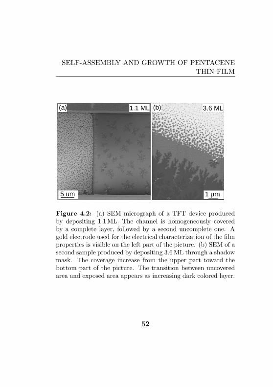
Fig. 4.2(a) shows a SEM micrograph of a device obtained by de-positing 1.1 ML of pentacene at a rate of 0.03 ML/min. The channelis homogeneously covered by a first complete layer, with an addi-tional uncomplete second layer in form of dendrimers. The layer-by-layer growth is evidenced in Fig. 4.2(b), where 3.6 ML are depositedthrough a shadow mask. The top of the picture shows the low cov-erage area with the SiO2 appearing in a bright color. The coverageincreases toward the bottom part of the picture, where a first, a sec-ond and a third layer is visible as layers with increasing dark color.The grain boundaries in the first monolayer are not recognizable ei-ther by SEM nor by AFM. The grain size estimated by the nucleationdensity interferred from the upper part of Fig. 4.2(b) should not belarger that 1 µm, but it can not be excluded that a number of thegrains merge together forming larger single crystals.
Fig. 4.3(a) shows an AFM measurements of the sample presentedin Fig. 4.2(a). The height of a single layer is found to be approxima-tively 1.5 nm (Fig. 4.3(b)), which corresponds very well to the lengthof a pentacene molecules (15 A).
These results are also confirmed by XRD measurements on asample with ∼6 ML presented in Fig. 4.4. Because of small thicknessof the investigated samples, the peaks are broad. However, threemain peaks associated to the pentacene layer can re recognized. The
51
SELF-ASSEMBLY AND GROWTH OF PENTACENETHIN FILM
5 um 1 µm
(a) (b)1.1 ML 3.6 ML
Figure 4.2: (a) SEM micrograph of a TFT device producedby depositing 1.1 ML. The channel is homogeneously coveredby a complete layer, followed by a second uncomplete one. Agold electrode used for the electrical characterization of the filmproperties is visible on the left part of the picture. (b) SEM of asecond sample produced by depositing 3.6 ML through a shadowmask. The coverage increase from the upper part toward thebottom part of the picture. The transition between uncoveredarea and exposed area appears as increasing dark colored layer.
52

4.4. STRUCTURAL CHARACTERIZATION
0 1 2 3-2
-1
0
1
2
µm
nm
(b)
(a) 5 nm
Figure 4.3: (a) 3µm×µm AFM scan of the sample presentedin Fig. 4.2(a). (b) line scan showing that the surface is almostcompletely covered by a 1.5 nm layer. The dendrimer growingan top of it is also 1.5 nm height, confirming the layer-by-layergrowth mode.
53

SELF-ASSEMBLY AND GROWTH OF PENTACENETHIN FILM
1 2 3 4 5 6
102
103
104
theta (°)
calib
rate
d co
unts
↓
(001)
↓
(002)
↓
(003)
SiO2/Si
Pn/SiO2/Si
0 0.1 0.20
1
2
3
2sin(θ)n
λ (Å
)
d = 15.3 Å
(a)
(b)
15.3 A15.3 A
Figure 4.4: (a) XRD spectrum of 6 ML pentacene deposited onSiO2(50 nm)/Si surface. The peaks corresponding to the penta-cene crystal lattice are evidenced. (b) Crystal structure of thethin film phase. Reprinted from [49]
54

4.4. STRUCTURAL CHARACTERIZATION
position at 1.85, 3.85 and 5.80 corresponds to a lattice constantof the (00l) planes of the pentacene crystals of 15.3 A for the 1th,2th and 3th order diffraction peaks, respectively. This is in excellentagreement with crystallographic studies on the pentacene thin filmphase [53, 54, 55].
From these results, it is concluded that the produced samplesconsist of polycrystalline thin film composed by pentacene moleculesstanding in the upright position. The molecules pack together result-ing in ordered monolayer domain that grow in layer-by-layer fashion.These growth conditions are exploited for the production of the fewML thin film transistor presented in Chap. 6.
It is important to note, that the growth is different if the sampleare not quickly transferred to the deposition chamber after the lastoxygen plasma cleaning process. Otherwise, extended air exposureof the SiO2 surface leads to multilayer islands and the productionof uniform samples with few ML pentacene coverage is not possible.The contaminations from the environment change the surface com-position and consequently the surface energy ,which probably changethe diffusion/flux ratio and therefore the growth mode.
4.4.3 Pentacene on metal surfaces
The growth of ultrathin layers of pentacene on metal substrate differsfrom the growth on oxide surfaces. On a metal surface, the electronicsurface states of the metal extend into the vacuum as evanescentwaves, which strongly interact with the molecular orbitals. On goldsingle crystal, the pentacene exhibit a flat-lying phase [56], where themolecules are oriented with their long axis parallel to the substrateand growth in a layer-by-layer cofacial structure, provided that abalance between intermolecular interaction and molecularsurface in-teraction is achieved. In case of polycrystalline surfaces, this balancecan change depending on the details of the surface as shown in this
55

SELF-ASSEMBLY AND GROWTH OF PENTACENETHIN FILM
section. The metal surfaces studied in this dissertation are polycrys-talline gold and palladium surfaces used as electrodes for the TFTs(Chap. 6) and the gold electrode of the nanojunctions (Chap. 3).
The electrodes used in the TFTs are made by depositing on ox-idized p-Si substrates 10 nm Ti adhesion layer followed by 200 nm ofAu or Pd. For all these surfaces, the deposited pentacene form multi-layers round-shaped islands as depicted in the left side of Fig. 4.5(a),(b) and on Fig. 4.6(a)
The growth of pentacene on metal is important first of all forthe characterization of the contact resistance of few monolayer TFT.In such few monolayer film, the morphology of the organic layer atthe transition between the metal electrode and the oxide surface iscrucial for a good electrical contact between the electrode and thepentacene channel. Fig. 4.5(a) shows an example of a bad contact,which leads to a pronounced contact resistance that strongly limitsthe performances. The device is obtained by depositing 1.8 ML at aperpendicular direction to the surface. It is recognized from the SEMimage that the region close to the interface grow in a peculiar way,with a strong tendency of dewetting. As a consequence, only a smallportion of the electrode is connected by pentacene to the channel.Although the electrodes patterning process is developped for obtain-ing a gently decreasing thickness by using a double layer resist and byrotating the sample during metallization, a local shadow mask effectcan decrease the amount as well as the rate of deposited moleculesclose to the electrode. This problem is minimize by depositing thefirst half of the pentacene at an angle of ±30, exposing equally theleft and the right contact regions. The process is terminated by theremaining part of pentacene deposited at a perpendicular direction.Increasing the channel thickness to 6-7ML further increase the ex-tent of the contact between the channel and the electrode as shownin Fig. 4.5(b). The device performance is enhanced, even if the chan-
56

4.4. STRUCTURAL CHARACTERIZATION
500 nm 500 nm
(b)(a)
Figure 4.5: (a) SEM of a electrode (left) with a bad contact tothe pentacene channel (right). Only a small island connect theelectrode to the channel. (b) SEM of a good contact, showingthat a much larger contact area between the pentacene islandon the electrode edge and the pentacene layer on the SiO2. Thesample is obtained by partially depositing the pentacene withan angle of ±30 with respect to the perpendicular direction.In this particular sample, an higher amount of pentacene is de-posited.
57

SELF-ASSEMBLY AND GROWTH OF PENTACENETHIN FILM
nel coverage appear less regular probably because of slightly differentevaporation condition or surface contamination. The considerationon the extent of the contact area responsible for the injection is im-portant for the investigation of the the contact resistance. Comparedto thicker devices or to top-contacted TFT, in few ML TFTs onlythe region close to the interface, i.e. only the channel width andthe pentacene coverage along the edge of the electrode, is important,while the two dimensional geometrical extent of the metal pad is not.The reason is that at these small coverages, the pentacene on theelectrode forms disconnected islands and can not contribute to theinjection of carriers in the channel.
A completely different growth mode is unexpectedly found byinvestigation of pentacene deposited on single gold layer that is usedas the electrodes for the nanojunctions. Only in this case, penta-cene self-assemble as several 100 nm-long rods with a diameter of∼20 nm (Fig. 4.6(b)). This growth mode (at a fixed growth rate of0.06-0.08, ML/min) strongly depends on the polycrystalline textureof the surface. This is clearly demonstrated in Fig. 4.6(c), wherethe metal surface on the left side of the picture is prepatternedby Ti(10 nm)/Pd(200 nm). The whole surface is then covered by90 nm Au, followed by pentacene deposition up to a nominal thick-ness of 4.2 ML. On the Au/Ti/Pd/SiO2 surface, pentacene grows in3-dimensional islands as illustrated above. However, on the Au/SiO2
surface, the molecules self-assemble in the form of nanorods.
It is worth to point out that the Au surfaces both sides, withand without prepatternd Pd/Ti layer, are prepared in identical con-ditions with the pentacene deposited in the same run. Moreover, agold thickness of 90 nm ensure a complete coverage of the underly-ing surface and a floating effect or diffusion of the underlying metalwhile gold deposition is not found in the literature. The self-assemblyof pentacene on a metal substrate critically depends on the elec-
58

4.4. STRUCTURAL CHARACTERIZATION
500 nm
Au / Pd / Ti / SiO2 Au / SiO2(c)
200 nm 200 nm
(a) (b)Pd / Ti / SiO2 Au / SiO2
Figure 4.6: SEM micrographs of pentacene deposited on dif-ferent metal surfaces covering a SiO2 substrate. (a) 1.4 ML de-posited on Pd(200 nm)/Ti(10 nm). (b) 4.1 ML on Au(90 nm).(c) 4.2 ML deposited on Au(90 nm). The Au layer extend overthe all sample, but on the left side, the surface is prepatternedby a Pd(200 nm)/Ti(10 nm), while on the right side Au is di-rectly evaporated on SiO2.
59

SELF-ASSEMBLY AND GROWTH OF PENTACENETHIN FILM
tronic structure of the metal [35]. Possibly, diffusion and and self-assembly also depend on the crystallographic orientation and on thestep edge density. XRD of gold deposited directly on SiO2 reveals apreferred (111) orientation, with additional other crystal facets, grainboundaries and step edges as visible in the SEM pictures. By tm-AFM measurements, the average roughness Ra for the Au/SiO2 andAu/Pd/Ti/SiO2 surfaces is found to be 1.5±0.5 nm and 3.5±0.5 nm,respectively. It is therefore plausible that the density of other crys-tal orientations and/or type of defects on the metal surface differ.The growth of the pentacene nanorods is apparently controlled by adelicate balance between the diffusion of the molecules on the tex-tured metal surface and π-π interactions between the molecules. Thedifferent diffusion of pentacene on the two surfaces is also suggestedby a close inspection of the SEM picture. The gold grains are bet-ter visible on the Au/Pd/Ti/SiO2 surface, indicating that 1-2ML ofpentacene completely cover the Au/SiO2 surface. Unfortunately, itwas not possible to determine the crystal structure of the nanorods byXRD. The ∼100 nm gold layer, necessary for the particular growth ofthe nanorods, increases the reflectivity of the surface at small anglesby several orders of magnitude. The intensity of the reflected x-raysmask the scattered signal from the pentacene crystal and no peakscorresponding to the pentacene layer could be identified. This makesa determination of the pentacene orientation (parallel or perpendic-ular to the surface) impossible. However, it is safely concluded thata small differences in the average atomic crystalline structure of apolycrystalline metallic surface directly influences the molecular self-assembling of nanoscale object by a delicate energetic balance. Thisprovide thous an interesting method to control a surface-mediatedself-assembly process by physically tailoring the substrate.
It was found out later, that the growth of pentacene nanorodswas already observed [57, 58]. However the use of such self-assembling
60

4.4. STRUCTURAL CHARACTERIZATION
was not recognized. In the next Chapter, this self-assembling processis exploited to grow nanorods across the nanojunction devices andto characterize the charge transport in organic semiconductor at thenanometer scale.
61

62

Chapter 5Electrical transport
through self-assembled
pentacene nanorods
In this Chapter, the self-assembly properties of pentacene are ex-ploited to obtain nanorods that bridge the gap of a metallic nano-junctions, allowing for the investigation of the electrical transportproperties. The characterization is performed in-situ, in air and ina cryostat with temperature ranging between 298K and 100K. De-pending on the doping of pentacene, either by air contamination orcoevaporation with a dopant molecules, different transport mecha-nisms are observed.
63

ELECTRICAL TRANSPORT THROUGHSELF-ASSEMBLED PENTACENE NANORODS
5.1 Contacting pentacene nanorods bya metallic nanojunction
As presented in Sec. 4.4.3, pentacene deposited at a rate of∼0.1 ML/min on a single layer gold surface self-assembles in a form of20-nm wide, several 100-nm long nanorods. When the deposition isperformed on a metallic nanojunction, the nanorods can grow acrossthe gap connecting the two electrodes. The deposition angle was setbetween 0 and +30 in order to facilitated the bridging of the gap.An example of the nanorods devices obtained by undoped pentaceneis presented in Fig. 5.1(b), where it is recognized that nanorods inthe junction area are sometimes wider than what is obtained on theplanar surface. Nevertheless, the 3-µm wide electrodes are connectedby ∼7 nanorods for a total width of ∼800 nm. Fig. 5.1(a) shows aschematic drawn of the nanojunction. Devices based on pentacenedoped by F4TCNQ (the molecular structure and the energy levels arepresented in Sec. 6.4) have also been obtained by coevaporation of thetwo molecules in a 3% ratio. It was found that the doped pentacenealso forms islands but self-assemble in a flatter and less regular shapeas depiced in Fig. 5.1(c). The different shape can be explained by therelatively high doping ratio and its influence on the crystal structure.However, the aspect ratio and the nanorods-electrode contact areaare similar (within a factor 2) and can not explain the very differentelectrical transport properties presented below.
5.2 Current-voltage measurements ofundoped and doped nanorods
The electrical characterization is performed by the measurements ofcurrent-voltage characteristics (I − V ) of the devices using a
64

5.2. CURRENT-VOLTAGE MEASUREMENTS OFUNDOPED AND DOPED NANORODS
500 nm
A
V
upper electrode
lower electrode
(a)
(b)
200 nm200 nm
(d)
200 nm
(c)
Figure 5.1: (a) Drawn of the nanojunction devices used formeasuring the transport properties of pentacene nanorods. (b)SEM micrograph of a nanorods device. The pentacene molecu-les (nominal thickness ∼6 ML) self-assemble in form of nanorodsthat grown over the gap of the nanojunction connecting the twoelectrodes. Upper electrode is referred to the gold electrodeabove the step, while lower electrode is at the bottom of thesidewall of the step. (c) SEM of a F4TCNQ doped pentacenedevice showing the different shape of the self-assembled islands.However, both undoped and doped nanorods have similar con-tact area to the metal electrodes. (d) SEM of a thick undopedpentacene nanojunction obtained by depositing ∼20 ML at arate of 0.7 ML/min.
65

ELECTRICAL TRANSPORT THROUGHSELF-ASSEMBLED PENTACENE NANORODS
Ketihley 236 as a voltage drive source meter for controlling Vsd
and measuring Isd with sub-pA precision. In order to keep this cur-rent resolution and to limit the parasitic capacitance, the instrument,which is provided with triaxial cables, is connected to the sample byusing appropriate cables, feedthrough and connectors. In the part ofthe setup where the use of triaxial cables was not possible (e.g. in-side the evaporation chamber and in the cryostat), single separatedwire with a thin insulation provide a satisfactory current resolutionsince the external noise is shielded by the metallic chamber. Highvoltage feedthrough are found to shows significant lower current leakcompare to compact multi-pin feedthrough and are therefore pre-ferred. The leakage current through the substrate is measured usinga Ketihley 2400. The data are acquired at a rate of ∼1 measure-ment/sec by a laptop provided with a Labview program that controlsboth instruments. Three different measurement setup configurationsare used: the in-situ characterization setup (Fig. 4.1), a commercialprobe station for the measurements in air and a cryostat for the tem-perature dependent characterization. For all three setup, the samemeasurements units are used. The bias applied between the upperand the lower electrode was swept at 0.05-0.2 V/s between ±2 V forthe undoped devices and between ±1 V for the doped ones.
Fig. 5.2(c) and (d) show the I − V of an undoped and a 3%F4TCNQ doped pentacene nanojunction devices measured in vac-uum and in air, respectively. The device obtained from pure penta-cene measured in vacuum shows an insulating behavior with currentbelow 5 pA for bias voltage up to 2 V. Since the current measurdedon an empty device (before the deposition of the pentacene) is evensmaller, the hysteresis and the current intensity recorded is relatedto the udoped nanorods and is not an experimental artefact. Theorganic semiconductor is in this condition depleted of carriers. Thisobservation is supported by the investigations on thin film transis-
66

5.2. CURRENT-VOLTAGE MEASUREMENTS OFUNDOPED AND DOPED NANORODS
−2 0 2−15
−10
−5
0
5
10
15
bias (V)
curr
ent (
pA)
← × 1/104
vacuum
−2 0 2−150
−100
−50
0
50
100
bias (V)
curr
ent (
pA)
← × 1/102
air
emptyundopeddoped
undopeddoped
Figure 5.2: (a) I − V of undoped and doped pentacenenanorods measured in vacuum. Comparison between the cur-rent measured in an empty device (before the pentacene evap-oration) and the undoped pentacene nanojunction shows thatthe hysteresis and the current intensity recorded is related tothe nanorods and is not an experimental artifact. Undopednanorods show a highly insulating (Schottky) behavior, whereasin doped pentacene the conduction increased by a factor 105. (b)I − V of undoped and doped pentacene nanorods measured inair. Undoped pentacene exhibits a rectifying behavior, while afully linear ohmic I −V is recorded for doped pentacene. Uponexposure to the air, the conduction of the undoped pentacene(at V =±2 V) increases by a factor 5-25, while the conduction ofthe doped pentacene decreases by a factor 20.
67

ELECTRICAL TRANSPORT THROUGHSELF-ASSEMBLED PENTACENE NANORODS
tor (TFT) based on the same material and at similar conditions.The transfer characteristics of undoped pentacene TFT presented inSec. 6.4 indicates a normally-off transistor (Isd = 0 at Vg=0), i.e.Vg,th < 0.
Upon doping, the current in the nanojunction increases to 150 nAat 2V. The effect is related to charge carriers that are introduced bythe doping process. Again, this can be compared to the positivevalues of Vg,th of the doped TFT presented in Sec. 6.4 and to therelated charge carrier density p0=4.8×10¹⁸ 1/cm3 that can estimatedfor a 3% doped pentacene. This increase is assigned to the doping-induced increase of the charge carriers density generated by a chargetransfer mechanism between the pentacene matrix and the dopant[59]. This interaction is investigated in detail in Chap. 6 and Chap. 8.In vacuum, the symmetric I − V of the doped nanojunction shows atransition from a linear regime below 0.2 V to a power law at higherbias voltages (I ∝ V α with α = 1.7 − 1.8 at V =±1 V).
This could be interpreted either as an indication for the trap fill-ing regime before the onset of a space charge limited current (SCLC)[60, 61] or as a Poole-Frenkel (PF) effect [62]. SCLC are usually onlypossibly in the most rigorously purified single crystal, which is notthe case here. However,the small channel length may be favorable toSCLC in spite of PF. Following Gregg et al. [63], the discriminationcan be made by comparing the charge carrier concentration p inducedby both mechanism. For this purpose, the I − V are first fitted bythe PF model
J = eFµ0pb,0exp((−Ea,0 + ηF 1/2)/kT ) (5.1)
where J is the current density (I/(Wd) with the width W=600 nmand the thickness d=10 nm ), F is the electric field (V/L with L=10 nm),µ0 the mobility, pb,0 the charge carrier density at zero filed (estimated
68

5.2. CURRENT-VOLTAGE MEASUREMENTS OFUNDOPED AND DOPED NANORODS
above), Ea,0 the activation energy and η describes the dependenceof µ and p on F 1/2. By setting σ0 = eµ0pb,0/(Wd)=7 × 10−8 Sfound by extrapolating the conductance at zero bias, the fit providesEa/kT=11 meV and η=2.77 × 10⁻⁵ eVcm/V1/2.
Since SCLC requires the bulk charge densitypb,F = pb,0exp(ηF 1/2/(kT )) to be insignificant compared to the in-jected carriers density pinj,F = Fǫǫ0/(eL), the ratio
ξ =pb,F
pinj,F(5.2)
needs to be much smaller than 1 for SCLC. After analysis of thedata, it is found ξ >1 for all the applied bias for the nanojunctionmeasured in vacuum, which would indicate a PF current. For dopedpentacene exposed to the air, the lack of knowledge on pb,0 and µ0
makes this analysis impossible. Moreover, ξ is quite sensitive to theincertitude in the actual device geometry. It is therefore concluded,that the I − V are not pure SCLC nor PF but an interplay betweenboth mechanisms probably exists. The important observation is thatboth type of descriptions are related to a bulk effect, i.e. the con-tact resistance in the doped pentacene nanojunction seems at leastcomparable to the bulk part. This issue will further be discussed inSec. 5.4.
For the undoped nanojunctions measured in air, a finite conduc-tion is recorded, probably because of charge carriers induced by aneffect of moisture, oxygen and light [64, 65]. From the TFT char-acteristics presented in Sec. 6.5, a charge carrier concentration of∼3×1017cm−3 is calculated, which is lower compared to the F4TCNQdoped pentacene (Sec. 6.4.2). The measured I − V are strongly non-linear and asymmetric. By a 3% F4TCNQ doping, the conductionis enhanced by a factor 103-105 and shows an Ohmic behavior. Thisimplies that the dopant molecules has a fundamental influence to the
69

ELECTRICAL TRANSPORT THROUGHSELF-ASSEMBLED PENTACENE NANORODS
transport properties on the nanometer scale.
To gain insight on the transport mechanism, temperature depen-dent measurements are presented in the next Section.
5.3 Temperature dependence of the con-ductivity
5.3.1 Experimetal setup
For the temperature dependent studies, all the sample have to betransferred from the evaporation chamber to the low temperaturemeasurements setup, exposing therefore the samples to the air forabout 5min. The setup consists of a close cycle He-cryostat (Janisxxx) with a base pressure below 1×10⁻⁶ mbar. The same measure-ments units as for the in-situ characterization is used.
5.3.2 Results on doped pentacene
Fig. 5.3(a) shows the I−V of a doped nanojunction measured at tem-peratures ranging from 298 K to 101 K. The curve are linear, showingan Ohmic conduction for all investigated temperatures. If a simplethermal activated transport I(T )/V = G(T ) = G0exp(−Ea/(kBT ))is assumed, the activation energy Ea can be calculated from the slopeof the Arrhenius plot log(G(T )) vs. 1/T . The results presented inFig. 5.3(b) show that this model fits very well the transport in thedoped nanorods device with an activation energy Ea=128±4 meV.By comparing the conductance before and after the thermal cycle, a10% lower conductace after the cycle is recorded, which indicates anacceptable low degradation.
70

5.3. TEMPERATURE DEPENDENCE OF THECONDUCTIVITY
−1 0 1−10
−5
0
5
10(a)
bias (V)
curr
ent (
nA)
298 K277 K261 K242 K222 K202 K181 K161 K141 K121 K101 K298 K
4 6 8 10
10−12
10−11
10−10
10−9
10−8
1000/T (1/K)
G (
S)
(b)
Ea = 128 +/− 4 meV
Figure 5.3: (a) I-V characteristics of a doped pentacene nano-junctions measured at temperature between 298 K and 101 K.A striking linear behaviour is observed at all temperatures. (b)Arrhenius plot of the conductance showing a thermal activationenergy of 128±4 meV.
71

ELECTRICAL TRANSPORT THROUGHSELF-ASSEMBLED PENTACENE NANORODS
5.3.3 Undoped pentacene nanorods
The transport mechanism in undoped pentacene nanorods device isvery different from the doped ones. The asymmetry, already pre-sented in Sec. 5.2, further extends to the temperature dependence.Fig. 5.4(a) shows the I−V measured at temperatures between 298 Kand 200 K. The raw data has a quite large scatter (cf. the I − Vof undpoed nanorods in air in Fig. 5.2), therefore an averaging pro-ceed over three consecutive scans is applied. In Fig. 5.4(b) the cur-rent measured at different bias is plotted versus the inverse of thetemperature. An Arrhenius model describing the transport requiresthat the points, representing the current measured at the same bias,should be aligned, where the slope of the line represents the activationenergy. This is clearly not the case, and the transport mechanism ap-pears to be more complicated. The slope of the curve in Fig. 5.4(b)is attributed to some activation energies (that depend on tempera-ture and on bias). The transport is almost temperature independentfor negative bias, while for positive bias the activation factor reaches∼300 meV for intermediate temperature. The increase of the conduc-tivity in some T-range could be ascribed to the electrical instabilityof the nanorods, probably given by some charges in the contact re-gion caused by the applied bias. However, the observation of differenttransport between positive and negative voltages is evident and is notinfluenced by changes in the contact region.
Although the experimental I −V curves could be reasonably fit-ted by a Fowler-Nordheim model (field assisted injection through atriangular shape energy barrier) for negative bias and by a Richardson-Schottky model [66](thermionic emission over an image potential low-ered energy barrier) for positive bias, it is difficult to unambiguouslydetermine a transport mechanism. Moreover, the measured tempera-ture dependence is not well described by these models. It was shownthat the obtained fitted parameter differs by order of magnitude from
72

5.3. TEMPERATURE DEPENDENCE OF THECONDUCTIVITY
−2 0 210
−14
10−13
10−12
10−11
10−10
10−9
(a)
bias (V)
I (A
)
T = 298 KT = 275 KT = 260 KT = 250 KT = 240 KT = 230 KT = 215 KT = 200 K
3.5 4 4.5 5
10−13
10−12
10−11
10−10
10−9
(b)
300 meV
100 meV
1000/T (1/K)
I (A
)
V= −2.0 VV= 2.0 VV= −1.0 VV= 1.0 V
Figure 5.4: (a) I-V characteristics of a pentacene nanorodsdevice measured at temperature between 298 K and 200 K. TheI-V curves are nonlinear and asymmetric. (b) The conductancedoes not follow a simple thermal activated behavior. Rather,the transport appears to be almost not temperature dependentfor negative bias (red symbols). A more complicated transportis found for positive bias (blue symbols), where the activationenergy reaches ∼300 meV for intermediate temperature.
73

ELECTRICAL TRANSPORT THROUGHSELF-ASSEMBLED PENTACENE NANORODS
theoretical ones [67], which cast a serious doubt on the applicationof such models in the case of metal-organic semiconductor interfaces.Therefore, the obtained results will only be qualitatively described.
It is noted by close inspection of the SEM image (Fig. 5.1(b)),that most of the nanorods have larger contact area to the upperelectrode compared to the bottom one, probably as a consequence ofthe electrode geometry and the growth mode of the nanorods. Thehypothesis that the different contact explain the asymmetric I − Vcharacteristics is discussed in Sec. 5.4.
To support this hypothesis, thick pentacene devices are producedby depositing ∼20 ML (deposition rate ∼0.7 ML/min) of pentaceneon a similar metallic nanojunction. The thick devices show that thegold surface and the gap region are almost completely covered withpentacene (Fig. 5.1(d)). Thus, the pentacene has similar contact onboth sides. As expected, the measured I−V are much more symmet-ric as depicted in Fig. 5.5(a). The temperature dependent transportcan be fitted at high bias by an Arrhenius model. In contrast to thedoped nanorods devices, the conductance G depends here on both thetemperature and on the bias. The results are presented in Fig. 5.5(b).For bias exceeding 1 V, an activation energy of 270-410 meV is found,which is slightly larger for positive compared to negative bias. Inthis regime the activation energy decrease with increasing bias. Thisobservation indicates a barrier lowering by the applied field. Theeffect is experimentally similar to the Schottky barrier lowering ininorganic semiconductor, but the exact injection mechanism betweena metal electrode and an organic semiconductor is different [68]. Atbias below 1 V, the Arrhenius model is less accurate, either becauseof experimental errors or because of a different injection mechanism.A discussion on the different injection processes observed is presentedin the next section.
74

5.3. TEMPERATURE DEPENDENCE OF THECONDUCTIVITY
−2 0 2
10−12
10−11
10−10
bias (V)
I (A
)
(a) T = 298 KT = 286 KT = 274 KT = 266 K
3.4 3.6 3.8 4 4.2
10−12
10−11
10−10
10−9
(b)
272 meV
359 meV
343 meV408 meV
376 meV361 meV
1000/T (K−1)
I (A
)
V= −2.0 VV= 2.0 VV= −1.0 VV= 1.0 VV= −0.2 VV= 0.2 V
Figure 5.5: (a) I-V characteristics of a thick (∼20 ML) pen-tacene nanojunctions measured at temperature between 298 Kand 266 K. The I-V curves are nonlinear but almost symmet-ric. (b) The current at different bias voltages shows a thermalactivation energy of 300-400 meV.
75

ELECTRICAL TRANSPORT THROUGHSELF-ASSEMBLED PENTACENE NANORODS
5.4 Possible transport mechanism
In this section, a possible mechanism for the transport observed inundoped and doped pentacene nanorods devices is discussed.
The first general consideration is on the size of the devices. Asthe channel length L is reduced, the interfaces become predominantfor the transport properties. This is because the total resistanceRtot is the sum of the contact resistance Rc and the resistance ofthe bulk part Rb, which depends on L. Reducing L increase the ratioRc/Rtot. It is known from literatures, that short channel effects startto play an important role in organic TFT with sub-µm channel length[69]. Since the here presented devices has L in the 10 nm range, itis not surprising that the interface is the bottleneck for the chargetransport. The second indication is based on the measured I − V .Usually, asymmetric I − V characteristics are obtained by using aselectrodes two metals with different work function. This is accom-plished by a sandwich structure with two different metals, as it isthe case in an organic light emitting diode or in photovoltaic devices.Asymmetric I−V are also observed by a combination of a clean elec-trode and a contaminated one. In both cases, the work function ofthe actual metal surface influences the energy level alignment of themetal-organic interface creating a build-in potential. In the here pre-sented devices, however, the two gold contacts have a similar amountof contaminations coming from the brief exposure to the air prior andafter the pentacene deposition. Consequently, the electrodes shouldexhibit the same work function. Nevertheless, the asymmetry hasto arise from contact properties, since the bulk do not discriminatebetween the flow in opposite directions. There is the possibility ofbipolar current caused by positive and negative bias, i.e. of transportof holes and electrons, which in general have different mobilities andcauses therefore different current intensity. Even if the transport inthe 10 nm range could be different, the TFT transfer characteristics
76

5.4. POSSIBLE TRANSPORT MECHANISM
presented in Chap. 6 suggest that holes are the main charge carriersin gold-pentacene-gold devices. Moreover, the results on the thicknanorods devices also imply that in case of similar contact on bothsides, the asymmetry disappears. It is therefore concluded, that thetransport in nanojunction device based on pentacene is determinedby Rc, i.e. it is limited by the charge injection from metal to pen-tacene at the contact. In other words, studying the transport innanojunction gives information about the injection properties of themetal-organic interface. The injection is governed by the HOMOalignment, interface dipoles and charge carrier concentration [68] or,more in general, by the shape of the energy band near the interface,by the barrier height and by the related depletion width. In a roughapproximation, the depletion width W at a metal-organic interfaceis determine by
W =√
(2ǫǫ0φ)/(pe) (5.3)
were φ is the band misalignment, ǫ the dielectric constant of penta-cene, p the charge carrier concentration and e the electron charge.As p is increased, W decrease and charges can more easily tunnelthrough the thinner barrier. As an estimation, the depletion widthW in the case of undoped pentacene exposed to the air, estimatedfrom p0 = 3 × 10¹⁷ and φ=0.4 eV, is 15 nm. It should be noted,that this relation follow from the Poisson equation applied to a pla-nar bulk junction. For a one-dimensional geometry, a deviation fromthis behavior has been both predicted [70] for carbon nanotubes. Ifthis has to be applied in a 10 nm organic semiconductor is still un-clear. The band missalignement [71] measured in UHV conditions isfound to be 0.47 eV [46]. Since the sample measured in these workhave been exposed to the ambient air, the contaminants probably re-duce the electronic interaction between the metal and the pentacenemolecules. The activation energy of 0.4 eV measured for the thicknanojunction is therefore in good agreement with the spectroscopy
77

ELECTRICAL TRANSPORT THROUGHSELF-ASSEMBLED PENTACENE NANORODS
experiments.
In the specific case of the thin nanorods devices, the nanorods-lower electrode contact, which has the smaller contact area, is moreexposed to the environment. As a consequence, the concentrationof the ionized dopants on the nanorods-lower contact is higher com-pared to the nanorods-upper contact. In the experiments, the voltagebias was always applied to the upper electrode (drain), while keepingthe lower one at ground (source). Thus, the width of the depletionlayer is considerably smaller on the source side compared to drainside. A possible band diagram is presented in Fig. 5.6. By apply-ing a negative bias voltage, the charge carriers (holes) have to beinjected from the source where the width of the depletion layer issmaller, allowing a direct tunneling through the barrier. This tun-neling process is inherently temperature insensitive, consistent to theexperimental data. In contrast, by applying a positive bias voltage,holes have to be injected from the drain where the width of the de-pletion layer is too large for a direct tunneling. Therefore the chargeshave to overcome a barrier by a thermally activated process charac-terized by an activation energy. This is also the case for the contactsin the thick devices, where both electrodes have a large contact areato the pentacene and the interfaces are therefore less exposed to theair. Consequently, the smaller charge carriers concentration and ahigher depletion width determine an almost symmetric I −V and anArrhenius-like activation energy.
This picture follows directly from the theory on inorganic semi-conductors. For metal-organic semiconductor interfaces, the situa-tion is more complicated because of the localized nature of the chargecarriers. In fact, the injection process involves a combination be-tween a thermionic emission process and a tunneling process, wherethe crucial first injection event is thermally assisted tunneling intoa distribution of localized states [68, 13]. The energy barrier that a
78

5.4. POSSIBLE TRANSPORT MECHANISM
tunnelingthrough the barrier
injectionover the barrier
doping Vsd
depletion width W
lower contact
uppercontact
Figure 5.6: Possible energetic levels of pentacene nanorodsconnetcted between 2 electrodes. On the left side (lower elec-trode in fig. 5.1(b)) the nanorods-electrode contact is smallerand therefore more exposed to environment doping. The carrierconcentration at this side is higher, which shrink the depletionwidth enabling direct tunneling through the barrier. This pro-cess is not temperature dependent. On the right side (upperelectrode in fig. 5.1), the depletion width is bigger and the car-rier must be thermally injected over the barrier.
79

ELECTRICAL TRANSPORT THROUGHSELF-ASSEMBLED PENTACENE NANORODS
charge has to overcome or pass depends on many details, like the en-ergy level alignment between the metal Fermi level and the first layerof molecules (charge neutrality level [72], the metal induced broaden-ing of the density of the gap states in the first layer of molecules [73]and the dopant induced dipolar disorder [74]. In low mobility disor-dered organic semiconductors, also the back diffusion of the injectedcarriers driven by the image charge potential has to be considered.This could also play a role in the interface region, where the mobilitycan be reduced by the impurities. However, even if a detailed de-scription is complicated, the general observation that doping reducethe injection barrier holds also for the injection in the nanojunctionpresented here.
As state above, the transport in nanojunction probes the injec-tion properties of the metal-organic interface. It is not obvious if thisis true also for doped pentacene.
The I − V of F4TCNQ doped pentacene measured in vacuum(Fig. 5.2(a)) show an indication of SCLC or PF related phenomena,which is a bulk effect. After exposing the device to air, the conduc-tance decreases and a fully linear I − V is measured, which is alsoan indication of bulk transport. On the other hand, by scaling themeasured Rc (Chap. 7) to the nanojunction geometry, it is foundthat even if Rc is substantially reduce by doping, it is comparable tothe resistance of the channel, i.e. the nanojunction remains injectionlimited. However, it should be noted, that a precise comparison ofRc between TFT and nanojunction devices is not straightfords, asthe arrangement of the pentacene molecules may be not comparableand the higher field in a small length scale could modify the barrier.
The question remains even if the transport at variable tempera-tures is considered. The I − V remains linear (within the measure-ment accuracy) to the lowest measured T . A linear I − V is a signeither of bulk transport or a tunneling process. By assuming a tun-
80

5.4. POSSIBLE TRANSPORT MECHANISM
nel process, the thermal activation energy has then corresponds tothe T-dependence of the barrier width. The problem is that a linearI − V based on a tunnel process requires G = I/V ∼ exp(−W ),where W is the barrier width, and the experimental observation ofG ∼ exp(−1/T ) implies W ∼ 1/T . This is not consistent with aSchottky-like barrier determined from W ∼ p−1/2 by thermally acti-vated carriers p ∼ exp(−1/T ). By assuming the thermal generationof p, then one has to conclude that W = −log(p). Curiously, this be-havior was observed in doped carbon nanotubes and was attributedto 1-dimensional nature of the system [70]. However, it is hard tobelieve that this would also applied in the present situation. A moreplausible explanation can be found in a thermally assisted tunnelingmechanism [75, 76]. The linear I−V could be a consequence of multi-ple tunneling processes, while the thermal activation part come fromthe energy difference between the mean energy level of the carrierand the transport level. However, it is not clear why by increasingfiled the activation energy stays constant.
In conclusion, it is difficult to clarify if the transport in dopedpentacene nanojunctions in limited by the contact or by the chan-nel. Available literature data on similar structure with comparablechannel length are very limited, and non of them comments on linearI − V of organic semiconductors. In any case, the important findingis that the transport in a 10-nm length scale shows a linear, highcurrent density I − V upon doping with F4TCNQ. These propertiesare well suited for a good injection of charges carriers into the organicsemiconductor and may be important for future applications.
For a field and temperature dependent quantitative measurementof the contact resistance in this material system, organic thin filmtransistors with undoped and doped pentacene are investigated inthe next chapters.
81

82

Chapter 6In-situ doping of a few
monolayer pentacene thin
film
In-situ characterizations of thin film transistor (TFT) are presentedin this chapter. Experiments with ultrathin active channel repre-sents a new method for the investigation of doping phenomena ina few monolayer (ML) organic semiconductors, in a similar way towhat has been recently discussed for inorganic semiconductors [77].In combination with the transmission line method, this approach per-mits to study the effect of dopant molecules on the mobility and theinjection efficiency at the nanometer scale.
83

IN-SITU DOPING OF A FEW MONOLAYERPENTACENE THIN FILM
6.1 Thin film transistor: introductionand working principle
6.1.1 Design
The electrical transport properties of organic semiconductor have of-ten been characterized using the investigated molecules as the activematerials in the channel of a filed effect transistor (FET). Such tran-sistors consists of two contacts, source and drain, separated by a de-fined distance (called the channel length L) and connected togetherby the semiconductive channel. A third electrode, the gate electrode,is separated from the channel by an insulating layer and allows themodulation of the channel conductivity. Typically, a SiO2 or a SiNinsulating layer is used, but recently high dielectric nanocomposite[78] or self-assembled monolayers [79] have been explored.
Bottom gated devices with very thin channel thickness (from fewmonolayer to ∼ 100 nm) are called thin film transistor (TFT). Thecontact are usually made of metals, but in general can also be ob-tained from well-conductive polymer as it is the case for the so calledall-plastic (flexible) electronics. There exists two different configu-rations. Bottom-contact TFTs are produced by first pattering thetwo metal contact on a thin insulating layer and by then depositingthe semiconductive organic material in a last step of the fabricationprocess. The other possible configuration is the top-contact geome-try, where the two metal contact are produced in the last fabricationstep, usually by a shadow mask evaporation which permits to patternthe contact without damaging the semiconducting layer. The advan-tage of the bottom-contact FET is that the properties of the channellike e.g. the thickness or the composition can be easily changed onthe same device and the resulting characteristics can be continuouslymonitored. This is particularly helpful for studying the early stages
84

6.1. THIN FILM TRANSISTOR: INTRODUCTIONAND WORKING PRINCIPLE
of the channel formation (see Sec. 6.2) and the doping of the result-ing TFT (Sec. 6.4). The disadvantage is in general a poorer contactbetween the metal pad and the semiconductor because of the differ-ent growth of the film on the metal and on the oxide (as alreadypresented in Sec. 4.4). This issue is discussed in Sec. 4.4.3 and inChap. 7.
source Vsddrain
dielectric (SiO2)Vg
A
p+Si
channel thickness
pentacenechannel length
Figure 6.1: Schematic drawn of a bottom contact TFT. Inthese thesis, pentacene is used as organic semiconductor
6.1.2 Working principle
The advantage of using a FET for studying the transport propertiesof a semiconductor is that the conductivity of the channel, given byboth the carrier density and the charge mobility, can be indepen-
85

IN-SITU DOPING OF A FEW MONOLAYERPENTACENE THIN FILM
dently measured. The reason is that the gate bias voltage Vg linearlyinfluence the charge carrier density in the channel, whereas the mo-bility is in a first assumption independent from the applied field andfrom the charge carrier density. To illustrate the working principle,the energetic band diagramm of a p-type TFT is displayed in Fig. 6.2with a metallic gate electrode. A cut in the perpendicular directionp-p′ (Fig. 6.2(a)) show the allignement of the gate Fermi level EF ,the wide bandgap insulating oxide, the position of the high occupiesmolecular orbital (HOMO) and of the low unoccupies molecular or-bital (LUMO). For a p-type semiconductor, the states responsible forthe conduction (conduction states) lie close above the HOMO level.If no bias is applied to the gate (Fig. 6.2(a) and (b)), the Fermi levelEF lie somewhere between the HOMO and the LUMO of the organicsemiconductor. In this situation the conductivity of the channel isvery poor as the HOMO levels are not aligned to EF as sketched inthe horizontal cut h-h′ presented in Fig. 6.2(b). By applying a neg-ative bias between the gate and the two contact, an electric field iscreated in the channel. This shifts all the levels of the semiconductortoward positive values (Fig. 6.2(c). For large enough Vg conductionstates (holes) start to be aligned with EF (Fig. 6.2(d)) enabling thecharge carriers to flow between source and drain. This voltage is theturn on voltage Von. Around and below Von there is the subthresholdregime, where charges are partially free to move. Only above the gatethreshold voltage Vg,th, the number of induced charges contributingto the current increase proportionally with Vg.
6.1.3 Extrapolation of TFT mobility and chargecarrier density from measurements
Because of charge neutrality, the charge carrier concentration p gener-ated by Vg (above the gate threshold voltage Vg,th) can be expressed
86

6.1. THIN FILM TRANSISTOR: INTRODUCTIONAND WORKING PRINCIPLE
d s
p-typeoxide
gate
VG
source
gate
drainoxide
p
h’
p’
h
aa bb
cc dd
EF
HOMO
LUMO
p-p’ h-h’VG = 0
VG < 0
Figure 6.2: Working principle of a TFT. For simplicity bandbending at the oxide-pentacene interface at Vg=0 is neglected.In the experiments a p+-Si substrate is used as the gate elec-trode.
87
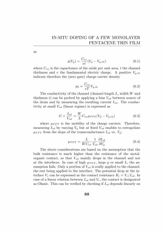
IN-SITU DOPING OF A FEW MONOLAYERPENTACENE THIN FILM
as
p(Vg) =Cox
et(Vg − Vg,th) (6.1)
where Cox is the capacitance of the oxide per unit area, t the channelthickness and e the fundamental electric charge. A positive Vg,th
indicate therefore the (zero gate) charge carrier density
p0 =Cox
eTVg,th (6.2)
The conductivity of the channel (channel length L, width W andthickness t) can be probed by applying a bias Vsd between source ofthe drain and by measuring the resulting current Isd. The conduc-tivity at small Vsd (linear regime) is expressed as
G =Isd
Vsd=
W
LCoxµTFT (Vg − Vg,th) (6.3)
where µTFT is the mobility of the charge carriers. Therefore,measuring Isd by varying Vg but at fixed Vsd enables to extrapolateµTFT from the slope of the transconductance Isd vs. Vg:
µTFT =L
WCox
1
Vsd
∂Isd
∂Vg(6.4)
The above considerations are based on the assumption that thebulk resistance is much higher than the resistance of the metal-organic contact, so that Vsd mainly drops in the channel and notat the interfaces. In case of high µTFT , large p or small L, the as-sumption fails. Only a portion of Vsd is really applied to the channel,the rest being applied to the interface. The potential drop at the in-terface Vc can be expressed as the contact resistance Rc = Vc/Isd. Incase of a linear relation between Isd and Vc, the contact is designatedas Ohmic. This can be verified by checking if Isd depends linearly on
88

6.1. THIN FILM TRANSISTOR: INTRODUCTIONAND WORKING PRINCIPLE
Vsd for small Vsd, i.e. before starting the saturation regime. The ef-fect of a large (ohmic and non-ohmic) Rc are noticed as non constantslope of the transfer characteristics, with in extreme case a saturationof Isd. For practical application, high Rc’s are undesiderable becauseof the decrease of Isd, of the on/off ratio and the performance. It istherefore important to characterize the potential drop in the contactregion.
6.1.4 Correction for contact resistance: trans-mission line method (TLM)
W = 110 µm
L = 20, 50, 75, 200 µm
resist opening
contact pads
pentacene
Figure 6.3: Schematic drawn of the devices used for the TLM:4 devices with L=20-200 µm are obtained by depositing penta-cene in the resist opening between the metal pads.
Several methods have been implemented for the measurementsof Rc: 4-probes technique [80], kelvin probe [81] and transmissionline method (TLM) [82]. In this dissertation, the TLM is used. Itconsists of measuring the total resistance Rtot of four TFTs withvarious channel length’s L and fixed width W (Fig. 6.3). Here Rtot
89

IN-SITU DOPING OF A FEW MONOLAYERPENTACENE THIN FILM
is expressed as the sum of Rc and Rb, which depends on L and thesheet conductivity σ. By using the relation
Rtot =Vsd
Isd= Rc + Rb = Rc +
L
Wσ= Rc +
L
WCoxµcf (Vg − Vg,th,i)(6.5)
Rc is evaluated by extrapolating to L =0 the relation between Rtot
and L:Rc = Rtot(L = 0) (6.6)
while the contact free mobility µcf is calculate by
µcf =1
WCox·
∂
∂Vg
(
∂Rtot
∂L
)
−1
(6.7)
An important assumption here is that the mobility is consideredfield independent, which should be considered for channel length de-pendent studies on the mobility at high Vsd. The Vg,th,i is the intrin-sic gate threshold voltage, which differs from the Vg,th extrapolatedfrom the transfer characteristics. It has been pointed out, that Vg,th isa fitting parameter without a real physical meaning [83]. Thus, thetransfer characteristics of a TFT can be described at various tem-peratures without the need of Vg,th. However, Vg,th does reflect ina rough approximation the charge carrier density, following Eq. 6.2.Therefore, even if only indirectly, it is a useful fitting parameter. Thedifference between Vg,th,i and Vg,th is further discussed in Sec. 6.3.
6.1.5 Considerations on the models, peculiar-ities of organic semiconductors
Although the above described model will be exploited in some mea-surements in this thesis to estimate µTFT and Vg,th, it is importantto point out some limitations.
90

6.1. THIN FILM TRANSISTOR: INTRODUCTIONAND WORKING PRINCIPLE
First of all, the onset of the conduction, i.e the region Vg > Vg,th
also referred as subthreshold region is not considered. It is knownfrom the literature and from experiments, that the onset is often notsharp and it is related to the effect of traps [84]. At higher negativeVg, these effects are less important as the traps get increasingly filledby charges. In some cases, it is not obvious where this transitionregion ends, and therefore the fit of the transfer characteristics isnot unique. In this thesis, the fit is always performed from the Vg
value corresponding to the highest slope. Second, the mobility isassumed to be field and charge carrier density independent in themodel. The dependence on the charge carrier density is presented inSec. 8.4. It will be shown, that at least for a doped pentacene TFT,the assumption of constant µ is not justified. By adopting the fittingprocedure described above, the evaluated mobility is approximatelyequal to the mobility at high charge carrier density. It is noted thatthe mobility can also be extrapolated from the saturation regime.However, e.g. in the in-situ monitoring of the TFT formation, alarge Vsd would possibly influence the pentacene growth.
The last observation is on the applicability of the TLM. Themethod could be used with success for all doped TFTs, at all tem-perature and channel thickness conditions. There are some slightdeviations from the foreseen linear dependence of Rtot at the higherL (Fig. 7.2), but these do not influence the extrapolated Rc or µcf
too much. However, for TFTs based on undoped pentacene, espe-cially at low temperatures, the linear relation between Rtot and Lis not fulfilled. Therefore the TLM can not be straightly applied inthese cases. In general it is observed, that if the contact resistanceis significant, Rtot decreases with increasing L from 20µm to 75 µm.This behavior could be a consequence of contacts that differ in theirresistance from device to device. This is plausible in the microscopicpicture by considering that a small difference in the number or shape
91

IN-SITU DOPING OF A FEW MONOLAYERPENTACENE THIN FILM
of the pentacene islands that cover the electrode edge can be re-sponsible for a large change in Rc. On the the hand, the Rtot vs.L relation seems quite systematic, which would not be expected inthese case. This behavior is not currently understood and the exper-imental data are simply not considered. It is noted that in the TLM,a field independent mobility is assumed.
92

6.2. IN-SITU CONTROL OF TFT FORMATION
6.2 In-situ control of TFT formation
6.2.1 Sample preparation
Using the above described bottom-contact TFT, the properties ofthe devices at increasing channel thickness can be measured. Theadvantage is that sample to sample variations that depend on manyexperimental parameters are reduced. The samples are produced bypatterning metal pads (gold or palladium) on a silicon wafer coveredby 50 - 150 nm of SiO2 grown by thermal dry oxidation. The separa-tion between the metal pads, i.e. the channel length L, are between20µm and 200 µm. The active part of the device is defined by open-ing a 50-110 µm wide window through a double layer resist over thecontacting pads and over the channel. This approach ensures a lowleakage current and a precise definition of the TFT geometry. Thesurface is cleaned by oxygen plasma for 30 s. After cleaning, up to4 devices on one chip are wire-bonded and loaded to the depositionchamber. The transfer takes approximatively 15min, therefore ex-posing the devices to ambient air. Longer exposure time is foundto have a detrimental effect on the transport properties and leadsin the extreme case to a unmesurable small currents. Probably thisis caused by the covering of the metal and the oxide by contami-nants. The so minimized exposure to the air may also affect theperformances, however since the extrapolated mobility is comparableto the values found in the literature, this effect is considered to besmall. The chamber is pumped down for 12-24 h to a base pressure of∼10−8 mbar. The evaporation is performed as described in Sec. 4.3.Briefly, the pentacene is deposited at a rate of 0.3-0.6 ML/min up toa thickness of 6-7 ML. The devices are characterized in-situ at inter-mediate coverages. For some experiments aiming at the investigationof dopant molecules, a thin channel thickness of 1-3 ML is exposedto a subsequent evaporation of the dopant molecules from a second
93

IN-SITU DOPING OF A FEW MONOLAYERPENTACENE THIN FILM
crucible. While reaching a stable evaporation rate of the dopant, thesample is hidden from direct exposure to the source. Therefore, ashorter stabilization time for the dopant (∼10 min) compared to thestabilization time for the pentacene evaporator (∼1 h) is necessary toavoid significant contaminations.
6.2.2 Measurements setup
The measurements are performed in-situ in the same vacuum cham-ber used for the deposition of pentacene. This chamber is equippedwith a home made chip carrier holder fixed on a linear feedthrough.The electrical access to the samples is provided by a 7-pins electricalfeedthrough connected by flexible cables to the chip carrier holder(Fig. 4.1). This enables to move the device in and out of the molec-ular beam without modification of the electrical connections. More-over, the linear feedthrough can also be rotated along its longitudinalaxis, which allows to deposit the molecules at any arbitrary angle.The electrical measurements are made using the same instrumentsused for the characterization of the nanorods device (Sec. 5.2). Inaddition, the gate voltage Vg is supplied by a Keithley 2400 whichpermits a maximal gate bias of ±20 V and the measurement of thegate leakage current Ig. For all the presented results, only deviceswith Ig <10 pA have been considered.
6.2.3 TFT formation
By exploiting the deposition setup in combination with the in-situcharacterization, the formation of the TFT can be monitored. Forthis purpose, a device with L=40 µm, W=50 µm is exposed to theevaporation of pentacene molecules while applying Vsd=-1 V, Vg=-5V and measuring Isd. The results presented in Fig. 6.4 show thatIsd remains in the pA range up to a channel thickness t of 1.1 ML.
94

6.3. DETERMINATION OF THE MOBILITY ANDTHE THRESHOLD GATE VOLTAGE
At this stage, the evaporated pentacene forms separated monolayerislands. By increasing the coverage, the current suddenly increaseto few nA, indicating the formation of a percolating network of con-ductive pentacene islands. Further increase of t up to 6ML shows asecond slower increase of Isd to the 100 nA range. The change in theoverall increase of Isd at ∼2 ML seems to suggest a maximal mobil-ity already achieved at 2 ML [6, 7]. The steps visible in the currentintensity are caused by the TFT investigations that have been per-formed at intermediate channel thickness, which slightly modify thecharacteristics.
An example of the measured output characteristics (Isd vs. Vsd)of a device with t = 1.6 ML (W=200 µm, L=40 µm, oxide thicknesstox=50 nm) is shown in Fig. 6.5(a). The current Isd increases withnegative gate voltages Vg, indicating a p-type behavior. Fig. 6.5(b)shows the transfer characteristics of the same device (Isd vs. Vg).From this second plot, the influence of the contact resistance Rc isidentified as a decrease of the slope at higher currents. This is notobvious in the output characteristics, since Isd around Vg=0 is verylinear, which is commonly taken as an indication of a good contact.The mobility µTFT equal to 0.02 cm/(Vs) is extracted by a linear fitof the curve at the maximal slope, while the gate threshold voltageVg,th is the intercept of the linear fit with the abscissa.
6.3 Determination of the mobility andthe threshold gate voltage
The investigation of the channel thickness necessary to reach a sat-urated value of the mobility is important to provide information onthe extent of the accumulation layer. This has a precise physicalmeaning, as it shows how the motion of charges can be confined in
95

IN-SITU DOPING OF A FEW MONOLAYERPENTACENE THIN FILM
0 2 4 610
-14
10-12
10-10
10-8
10-6
Vsd = -1 VVG = - 5 V
p=10-8 mbar
I s-d
(A)
Channel thickness (ML)0 2 4 6
10-14
10-12
10-10
10-8
10-6
Vsd = -1 VVG = - 5 V
p=10-8 mbar
I s-d
(A)
Channel thickness (ML)
Figure 6.4: Isd current measured at Vsd=-1 V and Vg=-5Vwhile evaporating pentacene over a TFT. At a critical channelthickness of 1-2 ML the current suddenly increases and saturatesat 4-6 ML.
96

6.3. DETERMINATION OF THE MOBILITY ANDTHE THRESHOLD GATE VOLTAGE
−6 −4 −2 0−40
−30
−20
−10
0
10
20
30
40
50
60
Vsd
(V)
I sd (
nA)
Vg = −10 V
Vg = −8 V
Vg = −6 V
Vg = −4 V
Vg = −2 V
−10 −5 0
0
5
10
15
20
25
30
35
40
45
50
Vg (V)
− I sd
(nA
)
Vsd
= −2 V
Vg,th
(a) (b)
Figure 6.5: (a) Output characteristics of a pentacene TFTwith a channel thickness of 1.6 ML measured in-situ: Isd is plot-ted in function of Vsd (b) Transfer characteristics of the samedevice: Isd is plotted in function of Vg. The effect of the contactresistance is noted by a decrease of the slope at high currents.
97

IN-SITU DOPING OF A FEW MONOLAYERPENTACENE THIN FILM
organic semiconductors, which is important towards miniaturizationand towards an understanding of the transport process.
Using the in-situ measurements capability, the channel thicknesst can be increased in several steps and the devices characterized aftereach additional deposition. The evaporation rate is 0.04 ML/min andthe first 1.1 ML are deposited at an angle of +30 and -30 to thenormal surface direction respectively, in order to well cover the sideof the metallic pad. Additionally, devices with channel lengths from20 µm to 200 µm are processed in parallel and characterized with thetransmission line method (TLM, Sec. 6.1.3). This is important inorder to extract mobility data free of parasitic resistance effects. Foreach device at various t, Isd is measured by setting Vsd=-0.1 V andby scanning Vg between ±20 V at a rate of 0.2-1 V/s. The mobilityµTFT and Vg,th are determined from the transfer characteristics aspresented above.
Fig. 6.6 shows Rtot = Vsd/Isd of pentacene TFTs with channelwidth W =110 µm at different t and at Vg= -20 V. It is noted thatRtot increases proportionally to L below 80 µm. Therefore, using thedata in this L range, the contact free mobility µcf is calculated fromEq. 6.7. The influence of the channel thickness on the extracted µcf
is presented in Fig. 6.7. In comparison, the mobilities µTFT fromthe transfer characteristics of the TFTs with the different channellengths L are also plotted.
The results show that the contact free mobility µcf saturates att =∼3-4 ML. The measured µTFT depends on L: higher values ofµTFT are recorded for devices with long channel length L. Becausethe devices are processed in parallel, this excludes strong device-to-device variation and suggests an important contribution of the con-tacts on the measured mobility. In fact, the contact free mobilityµcf is ∼40 % higher than µTFT for the longest channel and a up to afactor 4 for the shortest one. This implies that µTFT is strongly in-
98

6.3. DETERMINATION OF THE MOBILITY ANDTHE THRESHOLD GATE VOLTAGE
0 50 100 150 2000
10
20
30
40
50
60
70
80
90
channel length L (µm)
Rto
t = V
sd ⋅
I sd −
1 (M
Ohm
)
Vg = −20 V
thickness
2.2 ML2.8 ML3.6 ML4.8 ML6.8 ML
Figure 6.6: Total resistance Rtot measured for undoped penta-cene TFTs with various channel length L and channel thickness.
99

IN-SITU DOPING OF A FEW MONOLAYERPENTACENE THIN FILM
2 3 4 5 6 70
0.05
0.1
0.15
0.2
0.25
0.3
0.35
0.4
channel coverage (ML)
mob
ility
µ (
cm2 /(
Vs)
)
µcf
from TLM
192 µm73 µm48 µm18.5 µm
Figure 6.7: Contact free mobility µcf of pentacene TFTs atvarious channel thickness. In comparison, the mobility µTFT ex-tracted from the slopes of the transfer characteristics of TFTswith different L is systematically lower. The difference is as-signed to the contact resistance that is neglected in the extrac-tion of µTFT . Error bars indicate the difference between the upand down scan of Vg in the measured data
100

6.3. DETERMINATION OF THE MOBILITY ANDTHE THRESHOLD GATE VOLTAGE
fluenced by the contact resistance and is underestimated with respectto the real µcf governing the charge transport in the thin film.
The measured µcf value are in agreement with the values foundin the literature for polycrystalline pentacene, which range from 0.5to 0.8 cm2/(Vs) (measured with TLM, [69]). For single crystal pen-tacene measured with a 4-point method and an air-gap field-effecttechnique, the mobility reach 20 cm2/(Vs) [80].
By comparing the transfer characteristics of TFTs with differentchannel lengths L, it is noted that not only µTFT , but also Vg,th
depends on both t and L. Fig. 6.8(a) shows the conductivity scaledby L/W of the same set of measurements used for the extractionof the mobility data. The black lines denotate the linear fit. It isrecognizable, that Vg,th increases with increasing t and decreasingL. The maximal shift between TFT with the same coverage t is aslarge as 4.7 V, while by comparing the shortest and the longest L,the maximal shift is 7.2 V. The dependence of t can be understood asan increase of p caused by the contribution of the grain boundarieswhich density per square area increasing with t. The dependence onL is more puzzling. In the saturation regime (i.e. in case of Vsd ≫
Vg) it is attributed to a drain lowering of the Schottky barrier [85],where the source-drain field depends on L for fixed Vsd and on Vg.This can not be the case in the linear regime, where the source-drainfield is much lower that the gate field. A plausible explanation isthat Vg,th suffers from Rc since it is extrapolated from the transfercharacteristics that are clearly influenced by the contact properties.Fig. 6.8(b) shows the conductivity, scaled by 1/W obtained by theslope of the relation Rtot vs. L at Vg from 0 to -10 V (Eq. 6.5). Theintrinsic Vg,th,i, identified by the intercept of the linear fit with theabscissa, is about 10 V and varies only by 2.4 V for different channelthickness. This value is close to Vg,th for the longest L (Fig. 6.8(a)),confirming the importance of the contact resistance on the precise
101

IN-SITU DOPING OF A FEW MONOLAYERPENTACENE THIN FILM
determination of the characteristics of short channel TFTs.The good quality of the obtained device presented above allows
the use of TFT with ∼2 ML channel thickness. These devices are aninteresting new tool to study the interaction effects of dopant mole-cules directly deposited on top of the channel in a sub-ML coverage.The same devices are also well suited for the investigation of the ef-fect of pentacene TFT exposed to the air. These are the topics of thenext two sections.
102

6.3. DETERMINATION OF THE MOBILITY ANDTHE THRESHOLD GATE VOLTAGE
−20 −10 0−1
0
1
2
3
4
5
6
7
8
9x 10
−8
Vg (V)
σ =
L/W
× I sd
/Vsd
(S
)
L=192 µm
L=18.5 µm
6.8 ML4.8 ML3.6 ML2.8 ML2.2 ML6.8 ML4.8 ML3.6 ML2.8 ML2.2 ML
−20 −10 0−1
0
1
2
3
4
5
6
7
8
9x 10
−8
Vg (V)
σ =
1/W
× (
∂(V
sd/I sd
)/∂L
)−
1 (S
)
6.8 ML4.8 ML3.6 ML2.8 ML2.2 ML
Figure 6.8: (a) Conductance obtained from the transfer char-acteristics of a TFT with L=18.5 µm and L=192 µm at variouschannel thickness. From the linear fit, Vg,th varies between -3.4 and -10.5 V. (b) Conductance obtained from the TLM. Anintrinsic Vg,th,i of 10±1.2 V characterize all the TFTs.
103

IN-SITU DOPING OF A FEW MONOLAYERPENTACENE THIN FILM
6.4 Effect of guest dopant molecules
6.4.1 Control of threshold gate voltage by in-situ doping
TFT devices with a pentacene thickness of 1-3 ML are used to in-vestigate the effect of an evaporation of very low dose of a seconddopant molecule on top of the existing pentacene channel. The inves-tigated organic molecules are tetrafluoro-tetracyanoquinodimethane(F4TCNQ, Fluka), manganese(III)-tetraphenylporphyrin chloride(MnTPPCl) (Aldrich) and Fullerene (C60 ,Aldrich) used as received.Since a very low dopant coverage already modifies the transfer char-acteristics of the TFTs, a low evaporation rate of 0.02 ML/min isnecessary. This should also minimize the damages to the existingpentacene layer, which could lead to a decrease of the mobility be-cause of structural defects induced by the deposition. All measure-ments are performed in-situ and in the dark.
Figure 6.9(a) shows the transfer characteristics of a pentaceneTFT with L = 40 µm, W = 50 µm and channel thickness of ∼2 MLexposed to a subsequent evaporation of dopant molecules. The trans-fer characteristics is measured by applying a fixed drain-source bias(Vsd=-1, V for the MnTPPCl and Vsd=-0.1, V for F4TCNQ). Theeffect of the dopant molecules is characterized in terms of the shiftof the Vg,th and of the change of the mobility µTFT extracted fromthe transfer characteristics (Sec. 6.1.3). It is recognized, that theMnTPPCl molecules induce a decrease of Vg,th and of the mobilityµTFT . This is assigned to a n-type doping. It should be noted, thatthe effect is already noticeable at 0.2 mol% of , which represents amolecular surface density at the of 4.7×10¹¹. An opposite behavioris observed for the F4TCNQ molecule (Fig. 6.9(b)). The depositionshifts Vg,th towards positive values, which indicates an increase of thecharge carrier density p0 (Eq. 6.2). This observation is discussed in
104

6.4. EFFECT OF GUEST DOPANT MOLECULES
−10 −5 0−2
0
2
4
6
8
10
12
14
16
18
Vg (V)
− I so
urce
−dr
ain (
nA)
undoped0.2 mol%2.4 mol%2.6 mol%2.8 mol%3.1 mol%3.6 mol%4.7 mol%8.0 mol%13.6 mol%
−10 0 10−0.5
0
0.5
1
1.5
2
2.5
3
3.5
4
4.5
Vg (V)
− I so
urce
−dr
ain (
nA)
undoped0.7 mol%1.3 mol%1.8 mol%
Figure 6.9: Comparison of the effect of guest dopant molecu-les on the transconductance. (a) Doped with MnTTPCl. (b)Doped with F4TCNQ.
105

IN-SITU DOPING OF A FEW MONOLAYERPENTACENE THIN FILM
the next section. The mobility µTFT also appear to increase, but thisresult has to be carefully reflected. In fact, the detailed investigationspresented in Chap. 7 suggest that this effect is related to a decreaseof the contact resistance. The last observation is on the influence ofthe adsorbed C60, which have been evaporated on top of the penta-cene channel without modification of the electrical properties beingobserved.
Fig. 6.10 summarizes the shift of Vg,th for the investigated mole-cules. The minute variation of Vg,th for the three undoped devices is aconsequence of run-to-run variations and possible contaminations ofthe device during the stabilization time necessary to equilibrate theheated dopant crucible in order to reach a stable evaporation rate.
As stated above, the addition of F4TCNQ molecules promotes acharge transfer (CT) process between the pentacene and the dopantmolecules. This is tentatively explained by considering the ionizationenergy (IE = difference between the vacuum level and the HOMO)and the electron affinity (EA = difference between the vacuum leveland the LUMO) of the two molecules. A summary of the electroniclevels of the investigated molecles in prsentef in Fig. 6.11. From UPS-IPES experiments [36], the HOMO level of pentacene is observed at-5.0 eV and the LUMO of the highly electronegative F4TCNQ is ob-served at -5.2 eV. A transfer of an electron between the HOMO levelof pentacene to the LUMO of F4TCNQ (-5.2 eV) seems therefore en-ergetically favorable. This process would create a hole in the HOMOof the pentacene and lead to an increase of p. This is consistent withthe transfer characteristics being experimentally measured as shiftedto more positive gate values.
The situation for the MnTPPCl is more difficult to interpret,since the fact that the HOMO at -8 eV and the LUMO at -2 eV doesnot indicate a possible transfer of charges. A similar considerationon the electronic level can be made for C60, where the HOMO is
106

6.4. EFFECT OF GUEST DOPANT MOLECULES
0 5 10 15−8
−6
−4
−2
0
2
4
doping (mol%)
Vg,
th (
V)
F4TCNQC60MnTPP
Figure 6.10: Dependence of the threshold gate voltage on theamount of additional dopant molecules.
107

IN-SITU DOPING OF A FEW MONOLAYERPENTACENE THIN FILM
Mn-TPP-Cl F4-TCNQ
CNCN
CN CN
F
F
F
F
PentaceneF4-TCNQ (p doping)
- 2 eV
- 8 eV
- 3 eV
- 4.9/- 5.2 eV
- 5.2 eV
- 8.3 eV
-
+
-
+
E
Evac C60
- 4.6 eV
- 6.5 eV
N
N
N
NMn
Cl
Figure 6.11: Summary of the electronic level of the investi-gated molecules. A charge transfer doping process for pentaceneseems energetically favorable only with F4TCNQ
108

6.4. EFFECT OF GUEST DOPANT MOLECULES
located at -6.5 eV and the LUMO at -4.6 eV [86]. Indeed, no indica-tion of electronic interactions is observed between C60 and pentacene.The shift of Vg,th in the case of MnTPPCl can be explained by theexistence of energy levels in the bandgap, given for example by im-purites or by a partial thermal decomposition due to the evaporationprocess. The difference between MnTPPCl and C60, besides lowerthermal stability of MnTPPCl, is the existence of an electric dipoleand a magnetic moment given by the unpaired spin of the partiallyoxidized Mn atom. An exciting explanation of the shift of Vg,th andthe decrease of µTFT upon addition of MnTPPCl to pentacene couldtherefore be related to the electronic interaction of those dipoles withthe charges in the conducting layer. More experiments would benecessary in order to gain insight in this possible phenomena. How-ever, because of the improved transport properties of F4TCNQ dopedpentacene, the further investigations in the dissertation concern thislatter doping process.
6.4.2 F4TCNQ doping : effect on the carrierconcentration
The addition of F4TCNQ dopant molecules on top of a few ML TFTis now studied in detail: starting with TFTs devices with L=20 µmand 50 µm and W=110 µm, the dopant molecules are added in sev-eral subsequent steps. The evaporation and the characterization areperformed similar to the case described for the devices presented inSec. 6.4 except that a Vsd=-0.1 V is applied for the measurement ofIsd.
Fig. 6.12(a) shows the change of the transfer characteristics afterthe addition of the surface dopant, performed in several steps. Thefirst observation, already noticed in Fig. 6.9(b), is that the currentstrongly increases and Vg,th moves toward positive voltages. The
109

IN-SITU DOPING OF A FEW MONOLAYERPENTACENE THIN FILM
−20 0 200
5
10
15
20
25
30
35
Vg (V)
− I sd
(nA
)
−20 0 2010
−14
10−12
10−10
10−8
10−6
Vg (V)
undoped0.10 mol%0.31 mol%0.52 mol%0.77 mol%1.13 mol%2.19 mol%11.3 mol%
Figure 6.12: Evolution of the transfer characteristics of a TFTdevice with L=50 µm upon addition of F4TCNQ on top of a1.7 ML pentacene channel. (a) linear and (b) logarithmic plotof the transfer characteristics obtained by applying Vsd=-0.1 V.
110

6.4. EFFECT OF GUEST DOPANT MOLECULES
second observation is the decrease of the on/off ratio, i.e of the ratiobetween the maximal current at the Vg=-20 and the minimal currentat positive Vg. The undoped device shows an on/off ratio of 4×10⁴,while it decrease to 15 for the devices doped with 11.3 mol%. Thedecrease of the on/off ratio is ascribed to a strong increase of thecharge carrier density, which can not be electrostatically controlledby the gate voltage. This observation is in agreement with [59], butclearly limits the maximum amount of doping for obtaining a devicewith good dynamic range.
To quantify the number of doping induced charge carriers, thechange in the gate threshold voltage Vg,th is evaluated for a devicewith L=20 µm and L=50 µm. In Fig. 6.13 the shift ∆Vg,th relativeto the Vg,th of the undoped devices is plotted as a function of theamount of additional dopant.
The dopant ratio c is expressed in mol% relative to the totalamount of deposited pentacene (1.7 ML). The induced charge carri-ers concentration per unit area p is estimated from p = Cox∆Vth/e,where Cox is the oxide capacitance (2.4 × 10⁻⁸ F/cm2 given by the150 nm SiO2 used as gate dielectric). Below ∼1 mol%, p increaselinearly with c. The activation ratio η indicating the charges in-duced by a dopant molecules can therefore be calculated from rela-tion between p and c. Is is found that for L=20 µm, η is equal to1, while it decreases to 0.5 for L=50 µm. This dependence from Lis not well understood, but is probably related to the Vg,th depen-dence on L caused by the the extrapolation of Vg,th from the trans-fer characteristics without correcting for the contact resistance (seeSec 6.1.4). Nevertherless, this provides an estimation of the numberof charges produced by the charge transfer process between pentaceneand F4TCNQ. Since a longe channel TFT is less sensitive to the con-tact resistance, η is estimated to be in the range of 0.1, which wouldimply that in average 1 over 10 F4TCNQ molecule provides a hole to
111

IN-SITU DOPING OF A FEW MONOLAYERPENTACENE THIN FILM
0 2 4 6 8 10 120
2
4
6
8
10
12
14
16
18
dopant ratio c (mol%)
∆Vg,
th (
V)
η= 1.0 charges/dopant
η= 0.5 charges/dopant
L = 20 µmL = 50 µm
Figure 6.13: Shift of the gate threshold voltage by additionof F4TCNQ for a FTF with channel length 20µm and 50µm.The activation ratio η represents the induced charges pro dopantmolecule.
112

6.5. INFLUENCE OF AIR EXPOSURE ON THETHRESHOLD GATE VOLTAGE
the conductive pentacene channel. It is worth to note that the devi-ation form the linear relatioship appear at ∼1 mol%. Assuming thatthe deviation occurs when the influence area of the dopant moleculesstart to overlapp, it can be concluded that the radius of influenceof a dopant moleculeat is equal to the average distance between thedopant at ∼1 mol%, which corresponds to ∼5 nm. This is a rough ap-proximation that assume also that the dopants are well distributedon top of a perfect pentacene layer, but provides an estimation ofthe extention of the coulomb potential of the ionized dopant in a2-dimensional geometry.
6.5 Influence of air exposure on thethreshold gate voltage
In Sec. 5.2 it was shown that the conductance of pentacene nano-junctions increases upon air exposure. In order to quantify thisunintentional effect, TFTs with 2 ML pentacene channel (L=40 µm,W=50 µm for the TFT measured in vacuum, W=500 µm for the TFTmeasured in air) measured in-situ in the dark and in air with light.For these experiments, the characterization is performed by scanningVsd between +1 V and -5 V at each Vg. It is confirmed for both TFTsthat the Isd is linear at small Vsd, which permits to calculate theconductance by the slope ∂Isd/∂Vsd. The conductance normalizedby the device geometry is plotted in Fig. 6.14. The gate thresholdVg,th moves from -4 V for the TFT measured in vacuum to +4.3 Vfor the TFT measured in air. This indicate an increase of the chargecarrier concentration p0 to 3.3 × 10¹⁷ c/cm3 (Eq. 6.2) and a changeof the TFT from a normally-off (Isd=0 for Vg=0) to a normally-on(Isd 6=0 for Vg=0). The decrease of the slope upon air exposure isrelated to a decrease of the mobility µ. The measurements in air are
113

IN-SITU DOPING OF A FEW MONOLAYERPENTACENE THIN FILM
performed after ∼15 min of exposure to the air. With much longerexposure time, µ decreases further and finally the current become sosmall that it is not possible to measure the TFT properties anymore.It is concluded, that exposure to the air and light increases p butdecreases µ. A proper encapsulation would be required in order tostably operate the TFT in air.
114

6.5. INFLUENCE OF AIR EXPOSURE ON THETHRESHOLD GATE VOLTAGE
−10 −5 0 5 100
0.02
0.04
0.06
0.08
0.1
Vg (V)
σ =
I sd/V
sd ⋅
L / (
W ⋅
d) (
S⋅c
m−
1 )
Vg,th
= 4.3 V
TFT measured in vacuumTFT measured in air
Figure 6.14: Channel conductivity σ as a function of Vg of twoTFTs measured in vacuum and in air. The TFT measured inair shows a positive Vg,th, which indicates an increase of p uponair exposure.
115

116

Chapter 7Coevaporation of F4TCNQ
and pentacene
As recognized in Sec. 6.3, the contact resistance Rc of few ML TFTplays an increasing role, especially as the size of the devices is re-duced below the 10 µm range. Towards the miniaturization of or-ganic electronic devices and the improvement of their performances,it is therefore important to decrease Rc. In this section, the dopingschema for the reduction of Rc is investigated.
7.1 Reduction of the contact resistance
Following the procedure presented in Sec. 6.2.1, doped pentaceneTFTs are in-situ prepared and characterized. In order to keep the
117

COEVAPORATION OF F4TCNQ AND PENTACENE
−20 0 200
10
20
30
40
50
60
70
80
90
Vg (V)
− I sd
(nA
)
1.7 ML2.3 ML3.0 ML4.2 ML6.4 ML
−20 0 2010
−12
10−11
10−10
10−9
10−8
10−7
Vg (V)
− I sd
(A
)
Figure 7.1: Transfer characteristics for a (0.7±0.02) %F4TCNQ doped pentacene TFT with L=18µm at various chan-nel thicknesses.
118

7.1. REDUCTION OF THE CONTACT RESISTANCE
on/off ratio reasonably high, a low doping ratio of (0.7±0.02) % isused. This is achieved by evaporating a mixture of F4TCNQ andpentacene. The doping concentration c is estimated from the relationbetwee ∆Vg,th and c presented in the previous Chapter (Fig. 6.13) bycomparing devices with the same L. From the transfer characteristics(Fig. 7.1) it is found that the on/of ratio is 250 for the TFT withL=18 µm and the thickest channel coverage, but increases to 5×10³
at the thinnest coverage. The TFT with larger L have on/off ratiosin between these values. Using these data, the same analysis basedon the transmission line method (TLM) presented in Sec. 6.1.3 iscarried out. The results are presented in Fig. 7.2.
Comparing with the undoped TFT (Fig. 6.6), it is found thatthe linear relation between Rtot and L is improved up to the longestchannel devices. This is consistent to the model by Horowitz, wherethe mobility in polycrystalline organic TFT is limited by the grainboundaries, of which influence can be reduced by doping [87]. Fig. 7.3shows the extrapolated Rc for both an undoped and the doped TFTs.Rc includes the contribution of both source and drain contact. Theerror bars indicate the difference of Rc due to the hysteresis of Isd
between up and down sweeps of Vg. The hysteresis is not a conse-quence of the setup capacitance: an example of small hysteresis canbe seen in Fig. 6.5. For clarity, the up sweep has been omitted so far.
For both undoped and doped TFTs, Rc decreases with increasingchannel thickness T . The decrease is attributed to the increased uni-formity of the pentacene coverage at the edge of electrode contacts.This is concluded from SEM observations of the devices at differentchannel thickness prepared using the same conditions. For the un-doped TFTs, Rc reaches a minimum value of 7 MΩ at the thickestT=6.4 ML with Vg=-20 V. The Rc is 8 times higher compared to thereported values [82, 88]. This is ascribed to the small deposited pen-tacene thickness: in fact only the electrode edge is completely covered
119

COEVAPORATION OF F4TCNQ AND PENTACENE
0 50 100 150 2000
5
10
15
20
25
30
35
40
thickness
channel length L (µm)
Rto
t = V
sd /
I sd (
MO
hm)
Vg = −20 V
1.7 ML2.3 ML3.0 ML4.2 ML6.4 ML
Figure 7.2: Total resistance Rtot measured for F4TCNQ dopedpentacene TFTs with various channel lengths L and channelthicknesses.
120

7.1. REDUCTION OF THE CONTACT RESISTANCE
2 4 60
5
10
15
20
25
30
35
40
45
thickness (ML)
Rc (
MO
hm)
Vg= −20 V
Vg= −15 V
Vg= −10 V
2 4 60.2
0.3
0.4
0.5
0.6
0.7
0.8
0.9
1
thickness (ML)
Rc (
MO
hm)
Vg= −20 V
Vg= −15 V
Vg= −10 V
Figure 7.3: Extrapolated Rc using the TLM method as a func-tion of the channel thickness at various Vg for (a) undoped and(b) doped TFTs.
121

COEVAPORATION OF F4TCNQ AND PENTACENE
by pentacene while the surface of the electrode does not contribute tothe injection of the current in the channel, decreasing therefore theeffective area. Moreover, the contact resistance may also depends onthe thickness of the organic semiconductor above the metal surface.For the doped TFTs, Rc is ∼0.35 MOhm, which is a factor 20 smallerthan that of undoped TFTs. The Rc of the undoped TFT is about80% of the total resistance for a channel legth of 20 µm. For thedoped TFT, the Rc/Rtot decrease to 30 %. This indicates that theresistance of the channel is strongly reduced because of the additionalcharge carriers induced by the doping process, but the the resistanceof the contact region is even more influenced. The observation un-derlines the importance of Rc on the organic TFT performance.
For the undoped TFTs and at fixed T , Rc decreases when a morenegative Vg is applied. This indicates that the gate electric field isessential for the efficient injection of charges to the TFT channel.This can be compared to the Schottky barrier transistor in carbonnanotube [89]. The barrier height is determined by the band align-ment and the gate induced carrier concentration [90]. This enhancesthe thermionic emission over the barrier [91]. At the same time,the higher carrier concentration decreases the depletion width andenhances the (thermal assisted) tunneling through the barrier [92].Both processes lead to an enhancement of the carrier injection by Vg.
The situation is reversed for the doped TFT. First, the influenceof Vg is less pronounced. This is ascribed to the fact that the potentialprofile is here mostly determined by the ionized dopants [93]. Second,a detailed inspection of the data indicates a slight increase of Rc forVg below -10 V. It is noted that the increase of negative Vg leads tothe downward shift of the density-of-state (DOS) of pentacene chan-nel relative to the Fermi energy of the electrode while increasing theDOS filling by holes. Therefore, the decrease of Rc can be ascribed tothe decrease of DOS with Vg e.g. by saturating the states created by
122

7.2. COMPARISON BETWEEN THE MOBILITY OFUNDOPED AND DOPED TFT
the ionized dopants [5]. This reduces the thermal assisted tunnelingthrough the barrier by decreasing the available final states [13]. Onthe other hand, the increase of the hole concentration in the channelcan partially screen the impurity potential that counteracts the bar-rier lowering effect. Consequently the width of the interface barrieris increased. However, the screening property of the holes limited bythe hopping-like conduction in organic semiconductors has not beenclarified yet.
7.2 Comparison between the mobilityof undoped and doped TFT
The same data analyzed above also provides evidence that the mobil-ity is hardly affected by the ionized dopants. Fig 7.4 shows a compar-ison between the contact free mobility µcf measured using the TLM(Eq. 6.7) for the undoped a doped TFTs. Although µcf of the dopedTFT is slightly higher for a thickness smaller than 3 ML, it reaches asimilar saturation value of (0.35±0.05) cm2/(Vs) for increasing cover-age. The small difference in the early stage of the channel formationis explained by the importance of the grain boundaries at this stage.It was pointed out by Horowitz et. al [50], that back-to-back Schottkybarriers form at the intergrain regions. The barrier width depends onthe amount of defect states at the grain boundaries. It is thereforeplausible, that additional charges originating from the doping processdecreases these barriers and therefore enhances the measured mobil-ity. However, from the data presented here it can be concluded thatthis does not lead to a drastic change in the channel mobility at highgate voltage.
123

COEVAPORATION OF F4TCNQ AND PENTACENE
0 1 2 3 4 5 6 70
0.05
0.1
0.15
0.2
0.25
0.3
0.35
0.4
0.45
channel thickenss (ML)
µ cf (
cm2/
(Vs)
)
undopedF4TCNQ doped
Figure 7.4: Contact free mobility for undoped and F4TCNQdoped pentacene. The mobility is similar in both cases and issaturated at 3-4 ML. This shows the minimal influence of thedopant molecules on the hopping/scattering of the charges.
124

Chapter 8Thermally activated
transport in pentacene
In this section, the results of temperature dependent characteriza-tions of the TFTs are presented. For these measurements, the deviceshave to be transferred to the same cryostat which has also been usedfor the characterization of the nanojunction devices (Sec.5.3). Theexposure time to ambient air is kept to the minimal, typically ∼5 min.All the TFTs presented in this chapter have a channel length between20 µm and 200 µm, a channel width W of 110 µm, a gate oxide thick-ness of 150 nm and a channel thickness of 6-7 ML. In case of dopedTFTs, the TLM can be applied over the whole range of investigatedtemperatures. This allows to extrapolate the contact resistance Rc
and the contact free mobility µcf . These data are compared to the
125

THERMALLY ACTIVATED TRANSPORT INPENTACENE
mobility extracted from the transfer characteristics µTFT of undpoedand doped TFTs. In the last part of the chapter, the dopant inducedmodification on the density of states (DOS) in presented.
8.1 Temperature dependence of the mo-bility
Fig. 8.1 and Fig. 8.2 show some examples of the acquired transfercharacteristics at different temperatures. It is noted that because ofthe short exposure to the air, the characteristics are slightly differentfrom these which have been acquired in-situ. Most evident is theshift of the transfer characteristics of the doped TFT towards nega-tive voltages, which is assigned to a partial de-doping. However, theconclusions presented in this chapter are based on the difference be-tween undoped and doped TFT and are therefore not fundamentallyaffected.
From these data, the TLM is applied and the extracted contactfree mobility µcf at gate voltage Vg between -10 V and -18V is pre-sented in Fig. 8.3. An almost linear relation between log(µcf ) and1/T is found with a corresponding Ea of approximatively 95 meV forVg=-10 V, and slightly lower for more negative Vg. By carefully look-ing at the data, it is found that Ea is higher at lower T and no sign oftemperature independent mobility is found. This reflects the hoppingcharacter of the charge transport in these polycrystalline 6-7 ML thinfilm.
For comparison, an Arrhenius plot of the mobility µTFT calcu-lated from the fit of the linear part of the transfer characteristicspresented above is presented in Fig. 8.4. As stated in Chap. 7, thedoping process drastically decreases the contact resistance Rc. Thecalculated mobility should be therefore less affected by Rc and L.
126

8.1. TEMPERATURE DEPENDENCE OF THEMOBILITY
−20 0 2010
−14
10−13
10−12
10−11
10−10
10−9
10−8
Vg (V)
I sd (
A)
L = 20 µm, Vds
= −0.1 V
T ↑
−20 0 2010
−14
10−13
10−12
10−11
10−10
10−9
10−8
Vg (V)
I sd (
A)
L = 200 µm, Vds
= −0.1 V
T ↑295 K276 K256 K236 K216 K195 K175 K156 K136 K
Figure 8.1: Transfer characteristics of an undoped pentaceneTFT (left L=20 µm, right L=200 µm) at temperatures from295 K to 136 K.
127

THERMALLY ACTIVATED TRANSPORT INPENTACENE
−20 0 2010
−14
10−13
10−12
10−11
10−10
10−9
10−8
10−7
Vg (V)
I sd (
A)
L = 20 µm, Vds
= −0.1 V
T ↑
−20 0 2010
−14
10−13
10−12
10−11
10−10
10−9
10−8
Vg (V)
I sd (
A)
L = 200 µm, Vds
= −0.1 V
T ↑296 K271 K251 K221 K191 K171 K151 K131 K
Figure 8.2: Transfer characteristics of a F4TCNQ doped pen-tacene TFT (left L=20 µm, right L=200 µm) at temperaturesfrom 296 K to 131 K.
128

8.1. TEMPERATURE DEPENDENCE OF THEMOBILITY
3 4 5 6 7 810
−4
10−3
10−2
10−1
100
Ea = 95 meV
1000/T (K−1)
µ cf (
cm2 /(
Vs)
)
Vg = −18 V
Vg = −16 V
Vg = −14 V
Vg = −12 V
Vg = −10 V
Figure 8.3: Contact free mobility µcf of doped TFT at variousgate voltages. The mobility decreases with decreasing Vg andapproximatively follows a log(µcf ) vs. 1/T relation. An acti-vation energy of ∼95 meV is found for Vg = −10V and slightlydecreases with more negative Vg.
129

THERMALLY ACTIVATED TRANSPORT INPENTACENE
Consequently, Ea is less sensitive to injection processes and it is foundto varies between 102 and 78 meV for small, respectively large L, witheven a further decreases at higher T and large L. The similarity be-tween µcf and µTFT for TFTs with low Rc, both with respect to theT -dependence and to the extracted Ea indicates that the mobility ofdoped TFTs can also be calculated from the transfer characteristicswithout major contact artifacts.
For the undoped TFTs, it was not possible to apply the TLM atlow temperature (see Sec. 6.1.5). Therefore, only the µTFT extractedfrom the transfer characteristics is presented. Fig. 8.5 shows an Ar-rhenius plot of the µTFT for undoped pentacene TFTs. As expected,the so calculated µTFT is influenced by Rc (Sec. 6.3) and thereforeEa depends strongly on L.
At small L the effect of Rc is evidenced by the existence of twotemperature ranges with different Ea. In the high temperature range,µTFT is thermally activated with Ea=215 meV, while in the low tem-perature range Ea decreases to 93meV. Since a change from a lowerto an higher Ea with increasing T can not be explained by two dif-ferent processes acting in series (e.g. contact and channel), µTFT
reflects two ways for charges to be transported. The higher acti-vation energy Ea=215 meV is probably strong affected by contacteffects as thermionic or thermally assisted tunneling through the in-terface barrier. The value can be compared to the injection process inundoped nanorods (Sec. 5.3.3) which shows a value between 270meVand 360 meV. It should be noted however, that in TFT the gate fieldcan modify the injection barrier in a different way compared to biasfield in nanojunction devices. Moreover, the charge carrier density isprobably different, which would also change the shape of the bandbending at the interface. The part of the Arrhenius plot associatedwith the lower Ea is dominated by two contributions: a tunneling pro-cess through the barrier and the thermal activated transport in the
130

8.1. TEMPERATURE DEPENDENCE OF THEMOBILITY
4 5 6 7 8
10−4
10−3
10−2
1000/T (K−1)
mob
ility
µT
FT (
cm2 /(
Vs)
)
Ea = 78 meV
Ea = 102 meV
L ↑
190 µm71.5 µm47.5 µm18 µm
Figure 8.4: Thermal activation energy of the mobility µTFT
for F4TCNQ doped pentacene TFTs. An activation energy of78-102 meV is found for all 4 devices independently from thechannel length L.
131

THERMALLY ACTIVATED TRANSPORT INPENTACENE
channel (i.e. not influenced by the contact). The tunneling processcan be weakly temperature dependent because of a possible thermallyassisted contribution [94].
With increasing L, there is a progressive change to a single tem-perature regime. At large L, the contact has much less influence andµTFT is well described by a single activation energy of 71 meV.
From these data, it is concluded that the doping process hassmall influence on Ea. In fact, for large L, the doped and the un-doped devices have similar Ea. This is explained by the fact that Ea
is measured from µTFT , which is extracted from a linear fit of thetransfer characteristics either by starting at the maximum Vg or, incase of high Rc as the maximal slope. Therefore, µTFT reflects themobility at high Vg. In Sec. 8.5, the activation energy of the con-ductivity as a function of Vg is presented. It is found that at highVg, there are no differences in Ea between doped and undoped TFT.(Fig. 8.9). These latter activation energies also includes the activa-tion of the carrier concentration p. In the next section it will beshown through the analysis of the Vg,th shift, that the temperaturemay induce a change in the carrier concentration p only by a factor2 in the investigated temperature and gate voltage range. Comparedto the two orders of magnitude change of µTFT , the change in p isunimportant. It is therefore allowed to compare the Ea of the con-ductivity and of µ with the conclusion that at high Vg, both undopedand doped TFTs shows very similar thermal activated behavior. Infact, high Vg shifts the Fermi level well above the energy scale of thedopants, i.e. in the region where both undoped and doped pentacenehave similar density of states (see Fig. 8.9 and Fig. 8.10). However,it is expected that the contact free mobility measured at lower Vg isdifferent between undpoed and doped TFTS.
132

8.1. TEMPERATURE DEPENDENCE OF THEMOBILITY
3.5 4 4.5 5 5.5 6 6.5 7 7.5
10−4
10−3
10−2
1000/T (K−1)
mob
ility
µT
FT (
cm2 /(
Vs)
)
Ea = 71 meV
Ea = 215 meV
Ea = 93 meV
L ↑
192 µm73 µm48 µm18.5 µm
Figure 8.5: Thermal activation energy of the mobility µTFT
for undoped pentacene measured between 296 K and 131 K forvarious channel length L. For the TFT with L=18.5 µm, theactivation energy change from 93 meV to 215 meV at 230 K. Forthe TFT with L=192 µm, a single activation energy of 71 meVis found.
133

THERMALLY ACTIVATED TRANSPORT INPENTACENE
8.2 Temperature-induced shift of thegate voltage threshold
From the transfer characteristics, a temperature and L dependentgate threshold Vg,th is measured. The results presented in Fig. 8.6show that the shift ∆Vg,th drawn to scale Vg,th at T=298 K is similarfor undoped and doped TFTs and in a rough approximation is inde-pendent on L. It is found that ∆Vg,th is at the maximum 10 V, whichrepresents a factor 1/2 of the maximal applied Vg. It was pointed outby Meijer et al. [83], that Vg is merely a fitting parameter. The tem-perature dependence of Vg is governed by other underlying physicalparameters. However, since Vg,th is related to the carrier concentra-tion p, investigation on the T -dependance of Vg,th is important tohave information on the temperature induced variation of p. Theseconsiderations lead to the conclusion that the charge carrier densitydoes not strongly depend on T , so that any change of the conductiv-ity or the mobility by orders of magnitude (see previous section) cannot be determined by p.
134

8.2. TEMPERATURE-INDUCED SHIFT OF THEGATE VOLTAGE THRESHOLD
100 150 200 250 300−12
−10
−8
−6
−4
−2
0
T (K)
∆ V
g,th
(V
)
18 µm47.5 µm71.5 µm190 µm18.5 µm48 µm73 µm192 µm
undoped
F4TCNQ doped
Figure 8.6: Temperature induced gate threshold voltage shiftfor undoped and doped TFTs with various channel length Ldrawn to scale Vg,th at 298 K.
135

THERMALLY ACTIVATED TRANSPORT INPENTACENE
8.3 Contact resistance
The temperature dependence of the contact resistance Rc, extractedby the TLM from doped TFTs at Vg = −20 V is is plotted in Fig. 8.7.
Between room temperature and 190K, Rc increases accordingto the relation Rc = Rc,RT × exp(Ea, c/(kT )). The activation en-ergy Ea,c for this process is 0.16 eV. Below 190K, the behavior de-viates and the changes are less pronounced. The high temperatureregime is assigned to a thermally assisted tunneling of charge betweenthe metal electrode and the doped organic [75, 95]. The thermalcomponent of the tunneling process is here given by the probability∼exp(∆E/kT) that a charge hops between two sites having an en-ergy difference ∆E. By increasing T , there are more charges thatcan hop between more sites and therefore the process is thermallyassisted. The possibility of a thermionic emission process originatingfrom the thermal activated injection is excluded by the informationobtained from the doped pentacene nanojunction (Sec. 5.3.2). There,a linear IV is found from room temperature down to T=120 K whichshows that no substantial energy barrier is formed at the interface.At T below 190 K, there is a transition to a temperature indepen-dent Rc. In this T-range, a tunneling process could be the reason ofthe constant Rc. The same transition was observed in the contactresistance of carbon nanotubes []. It is therefore plausible that atthis gate voltage (Vg=-20 V) the barrier width at the interface be-tween metal and doped pentacene is thin enough allowing a directtunneling of charges. Vg seems also responsible for the missing tun-neling regime in the doped nanojunction, where no deviation froman Arrhenius-like behavior is observed.
136

8.3. CONTACT RESISTANCE
3 4 5 6 7 810
5
106
107
108
109
1010
1000/T (K-1)
RC
(Ohm
)
Ea = 158 meV
tunneling
thermally assisted tunneling
Figure 8.7: Temperature dependance of the contact resistanceRC at Vg=-20 V for a doped TFT. RC is calculated from tran-sistors with channel length from 20µm to 200µm as presentedin Chap. 7.
137

THERMALLY ACTIVATED TRANSPORT INPENTACENE
8.4 Charge carrier density dependenceof the contact free mobility at var-ious temperatures
In Sec. 6.1.2 the working principle of a TFT was presented. The ba-sic model assumes a mobility µ that does not depend on the carrierconcentration. It is shown here, that this is not true in doped fewML TFT. Again, using the TLM, it is possible to extract the contactfree mobility µcf for Vg between -20 V and 0V and at various tem-peratures. The gate induced charge carrier density p is calculatedby p = VgCox/(et), where Cox is the gate capacitance, t the chan-nel thickness and e the electronic charge. The result is presented inFig. 8.8.
It is found that the mobility µcf increases with increasing p. Thisobservation is consistent with a filling of the trap states by increasingp. At high Vg and corresponding increased p, part of the chargesneed a smaller activation energy in order to move, i.e. the mobilityincreases. At room temperature, the increase is about 1 order ofmagnitude over the applied Vg range. By lowering the temperature,the µcf dependence on p is increased, reflecting the fact that thethermal energy can contribute less to the hopping of the charges.The model proposed by Vissenberg and Matters [96, 97], based on avariable range hopping mechanism, shows
µ ∼ pT0
T−1 (8.1)
i.e. a linear dependence of µ from p in a double log scale. Here T0
describes the effective temperatures of the traps or alternatively thewidth of the exponential distribution describing the density of states(DOS). Although the stronger dependence of µ on p at lower temper-ature is correctly described by the model, the µ dependence at fixed
138

8.4. CHARGE CARRIER DENSITY DEPENDENCEOF THE CONTACT FREE MOBILITY AT VARIOUSTEMPERATURES
1017
1018
10−3
10−2
10−1
100
p (1/cm3)
µ cf (
cm2 /(
Vs)
)
296 K271 K251 K221 K191 K171 K151 K131 K
Figure 8.8: The contact free mobility of F4TCNQ doped pen-tacene in function of the charge carrier density at temperaturesbetween 296 K and 131 K.
139

THERMALLY ACTIVATED TRANSPORT INPENTACENE
T is experimentally found to be larger compared to the prediction.The deviation from the model is tentatively assigned to the shape ofthe DOS. In the model, an exponential DOS is assumed. In the nextsection, it will be shown that the DOS of the doped samples showedhere exhibit an additional broad peak as a consequence of the dopingprocess.
140

8.5. DENSITY OF STATES IN UNDOPED ANDF4TCNQ DOPED PENTACENE
8.5 Density of states in undoped andF4TCNQ doped pentacene
A fundamental aspect governing the charge transport in semicon-ductors is the density of states (DOS). In 3-dimensional inorganicsemiconductor materials, the DOS responsible for holes conductionis well described by a parabolic relation N(E) ∼ (E − Ev)3/2, whereEv is the upper energy of the valence band. Above Ev (and be-low the conduction band Ec) no states exists, i.e. there is a bandgap. In organic crystalline small weight semiconductors, the disor-der associated with the imperfect crystal structure given by the weakforces between molecules leads to a DOS that is usually modeled bya Gaussian or an exponential distribution. The consequence is anextension of the DOS into the gap region, commonly denominated asband tail. The introduction of guest molecules, either unintention-ally by contaminations or intentionally by doping, further modifiesthe DOS shape. Theoretical models describing the transport prop-erties are based on the knowledge of a statistical function describingthe energy distribution of charges. In order to apply the model toa physical situation and to compare with transport measurements,the determination of the DOS with respect of both shape and totaldensity is required [98].
In this Section, the transport in TFT at variable temperatureis exploited to extract the DOS [99, 5]. This is done by measur-ing Isd at a small Vsd=-0.1 V, fixed Vg and at various temperatures.The thermal activation energy Ea is then calculated according toIsd ∼ exp(−Ea/kT ). Assuming that the density of free carriers ismuch smaller than the density of trapped carriers N [100], the mea-sured Isd is given by the number of charges that are available in theenergy range for thermal activation. In a rough approximation, Ea
corresponds therefore to the energy difference between the Fermi level
141
THERMALLY ACTIVATED TRANSPORT INPENTACENE
EF and region close to the edge of the HOMO level. For practicalpurpose, the measurements are performed by scanning Vg at differ-ent temperatures and by extracting Ea from the measured Isd(Vg, T ).Fig. 8.9 shows a plot of the dependence of the extrapolated Ea onVg.
The DOS is defined as the number of states ∂N per energy inter-val ∂E. ∂N is given by ∂VgCox/e, where Cox is the gate capacitanceper unit area (2.4×10⁻⁸ F/cm2) and e the electronic charge. There-fore, the number of states N(E) is
N(E) =∂N
∂E=
Cox
e
(
∂Ea
∂Vg
)
−1
(8.2)
Calculating N(E) implies to differentiate the Ea values in Fig. 8.9with respect to Vg. The rather intriguing decrease of Ea at a certainVg is not understood. However, in order to avoid negative slopes inthe derivative, the calculation is performed by a piecewise linear fitof 7-13 points and all the results are plotted. This is a compromisebetween taking a small number of points and correspondly scatteringderivative, and taking too many points where the changes in Ea aresmeared out. The results are presented in Fig. 8.10, where N(E) isscaled by the channel thickness to give a volume density.
The DOS of the undoped pentacene can be divided in two regions.Below 0.15 eV the data are well fitted by a Gaussian distribution bysetting the total of states density equal to the density of pentacenemolecules (3.2×10²¹ c/cm3). The second region is fitted by an expo-nential part describing the tail above 0.15 eV. The exponential part
N(E) =Nt
kT0
exp
(
−E
kT0
)
(8.3)
relates N(E) to the trap density Nt and to an effective tem-perature T0. From the fit it is found N0=3.6×10¹⁹ and T0=1330 K.
142

8.5. DENSITY OF STATES IN UNDOPED ANDF4TCNQ DOPED PENTACENE
-20 -15 -10 -5 00
0.1
0.2
0.3
0.4
0.5
Vg (V)
Ea (e
V)
undopedF4TCNQ doped
2 4 6 810
-11
10-10
10-9
10-8
1000/T (1/K)
I sd (A
)
-20 V-10 V-5 V
Figure 8.9: Thermal activation energy Ea measured at variousVg for undoped and F4TCNQ dopend TFT pentacene.
143

THERMALLY ACTIVATED TRANSPORT INPENTACENE
0.1 0.15 0.2 0.25
1019
1020
Ea (eV)
N(E
) (eV
/cm
3)
undopedF4TCNQ doped
HOMO
E
DOS
F4TCNQ-
EF
Figure 8.10: Density of states N(E) of undoped and F4TCNQdoped 6-7 ML pentacene. The results are calculated from theTFTs data presented in Fig. 8.9 by applying Eq. 8.2.
144

8.5. DENSITY OF STATES IN UNDOPED ANDF4TCNQ DOPED PENTACENE
The T0 value is in very good agreement (within 5 %) with the valuereported by Lang et al. [99], which confirm the robustness of theapplied method.
The results on the trap density Nt are a factor 3 different fromthose reported by Lang et.al. The difference is ascribed to the ex-posure of the samples to the air. This is especially important in thedevices presented here, where the 6-7 ML thin channel is very sen-sitive to the air, even if the exposure time was minimized to 5min.The Gaussian distribution describing E below 0.15 eV is centered at-0.5 eV with a half width half maximum σ of 0.11 eV. These param-eters have to be taken carefully, since the fit is performed only overa small region of the distribution. However, the result is an usefulstarting point for the fitting of the doped TFT.
Clearly, the DOS of the doped pentacene is different from theundoped case, showing higher DOS with an additional broad peak.It is worth to note, that the peak does not arise from the fluctuationof Ea in the -5 V < Vg < 0V region of Fig. 8.9. Rather, the increasedN(E) is a consequence of the almost constant Ea values between -5and -10 V (Eq. 8.2). The peak in the DOS of doped pentacene isreasonably well fitted by an additional Gaussian centered at 0.14 eVwith σ of 0.012 eV. This peak is assigned to the F4TCNQ dopantsproducing additional trap levels located above the HOMO of penta-cene upon inclusion in the matrix. In Sec. 6.4 the molecular orbitalsof pentacene and F4TCNQ were presented. The difference betweenthe HOMO of pentacene ad the LUMO of the dopant is about 0.2 eV[36]. This is consistent with the observed position of the peak. Fora detailed picture of the doping process, information on dipole for-mation around the ionized dopant, morphological modification of thepentacene crystal and contribution from the grain boundaries arenecessary. However, some impact on the effect of the modified DOScan be drawn.
145

THERMALLY ACTIVATED TRANSPORT INPENTACENE
By carefully looking at the data presented in Fig. 6.12, the trans-fer characteristics of a 1.7 ML TFT shows some shoulder in the sub-threshold region. Similar observations were made by Mejer et al.[101]. There, the effect was attributed to the conduction through thethick channel far away from the interface. In the case of the devicesconsidered here, the channel thickness is ∼2 ML, therefore this mech-anism is rather improbable. The observed shoulders are tentativelyassigned to the transport through the dopant induced DOS. In fact,N(E) and therefore Isd does not vary monotonically as the Fermilevel is shifted by Vg from the unbiased position toward the middlegap. Rather, more energy levels become available as the Fermi levelapproach the center of the dopant induced DOS. The states involvedin the transport addressed by the Boltzmann distribution can there-fore vary in a non-monotonic way, producing a non-monotonic changein Isd, which is recorded as shoulders in the subthreshold part of thetransfer characteristics. An implication of these scenario, is that theFermi position at Vg=0 lies between the HOMO edge and the dopantinduced DOS. This hyphotesis is consistent with the ’normally on’state of the doped TFT and the decreased on/off ratio, since theFermi level can only be moved by Vg in a finite energy window.
An interesting final comparison that has to be made is betweenthe position of the doped induced peak in the DOS, the thermal ac-tivation energy of the I − V in doped nanojunctions (Fig. 5.3) andof Rc in doped TFTs ((Fig. 8.7). The observation is that, althoughmeasured in very different experiments, all these energies are veryclose. The thermal activation energy of the conduction in doped pen-tacene 10-nm channel measured with the nanojunctions is found tobe 0.123±0.002 eV. The contact resistance Rc measured in a 6-7 MLTFT geometry shows a thermally activated behavior with an acti-vation energy of 0.16 eV. This suggests that these three phenomenamay be related. It is recognized, that the injection of charges from a
146

8.5. DENSITY OF STATES IN UNDOPED ANDF4TCNQ DOPED PENTACENE
metal electrode to an organic semiconductor depends on the availablestates at in the second layer of molecules close to the interface [Ref].Since the doping induce additional states, the injection is enhanced.This is what is also experimentally observed by the reduction of Rc
by doping. In the nanojunction devices, the transport can hardlybe separated between interface injection and channel transport sincethe band bending occurs in a significant part of the channel. Themeasured activated transport could be therefore based on the samephenomena acting on Rc. This confirm that measuring the transportin a 10-nm channel is equivalent to measuring the injection proper-ties of the interface. In these scenario, the transport is no longer a3-dimensional effect but rather an interface phenomena.
147

148

Chapter 9Conclusions and Outlook
The electrical transport in organic semiconductor exhibits similarphenomena that are known from the bulk devices, spanning a largerange of length scales, down to the molecular dimension. In contrastto inorganic semiconductors, this fact offers a possibility to add newchemical functionalities to devices in the nanometer scale.
In this thesis, few monolayer-thick thin film transistors (TFTs)have been manufactured and characterised ’in-situ’. These devicesuniquely offer direct access to the quasi two dimensional active ma-terial layer. Thus, the manipulation of charge carrier density andthe transistor performance by dopant ad-molecules in controlled sub-monolayer concentrations have been studied. These experiments rep-resent a new method for the investigation of doping phenomena inorganic semiconductors. The characteristic effect of C60, MnTPPand F4TCNQ deposition at sub-monolayer coverage on top of a 2 ML-
149

CONCLUSIONS AND OUTLOOK
thick pentacene channel provides clear evidence for electronic interac-tions with the active material layer which are specific to the chemicalstructure of the dopant molecules. MnTPP, that has a large dipolemoment, shows a combination of decreased mobility and charge car-rier density, which can be assigned to a n-type doping process. Theaddition of C60, that is non-polar, shows no modifications of thetransport properties of the pentacene channel. The most strikingeffect is found when F4TCNQ is used as a dopant molecule: Here,the investigations show a p-type charge transfer doping process thatpermits both an increase of the charge carrier density and an improve-ment of the injection efficiency at the metal-pentacene channel inter-face without degradation of the channel mobility. The doping effi-ciency is estimated to be in the range of 0.1 charges/dopant molecule.By using the transmission line method (TLM), the channel mobilityµ of TFTs with 2-7 ML-thickness is measured without the influenceof the contact resistance. µ is found to be 0.35±0.05 cm/(Vs) forboth undoped and F4TCNQ doped TFTs, which is comparable tothe state-of-the art mobility of polycrystalline organic semiconduc-tors. This behaviour shows that the coulomb potential of the ionizeddopants is screened to a large degree. An approximately linear re-lation is observed, for both undoped and doped pentacene, betweenlog(µ) and the inverse temperature 1/T that evidences the impor-tance of hopping between localized states.
The exact physical origin of these striking phenomena relatedto the doping induced enhancement of the injection at the metal-organic interface has not been clarified yet. However important in-sight is obtained by temperature dependent transport in TFT geom-etry as well as in 10 nm-channel devices: The Schottky-like potentialbarrier between a metal electrode and an undoped organic semicon-ductor is revealed by the current-voltage characteristics measuredin a 10 nm channel device based on the metallic nanojunction spe-
150

cially developed for this study. The contact resistance at the metal-organic interface can be lowered by the gate field in thin film tran-sistor geometry with few monolayer channel. The effect, althoughon a nanometer scale, is similar to what is found in conventional in-organic semiconductors and in 1-dimensional conductor like carbonnanotubes. It is related to a potential barrier with finite thicknessthat results from a finite difference ∆E between the metallic workfunction and the ionization potential of the pentacene. The Scottkybarrier height of ∼0.4 eV has been determined from the tempera-ture dependent current-voltage characteristics of undoped pentaceneon a 10 nm-channel nanojunction. This value is consistent with theexpected ∆E of 0.47 eV.
However, the injection process can be controlled by doping en-gineering. The doping process here results in the local modificationof the potential landscape by the individual ionized dopant molecu-les. The radius of influence of a single dopant is estimated to befew nanometers, therefore a few % doping ensures a complete changeof the injection barrier at the metal-organic interface. In pentacenedoped with 3% F4TCNQ, a highly linear, ohmic transport regime ina 10 nm channel device is achieved with an enhancement of the con-ductivity by a factor of 103-105. In the TFT geometry, the contactresistance is reduced by a factor of 20 upon 0.7% F4TCNQ doping.The effect of the gate field on the contact resistance is in this casereverted, which confirms that the charge injection process at the in-terface is strongly modified by the ionized dopants.
At low temperature, the contact resistance in doped TFTs showsa thermally activated behavior with an activation energy of 0.16 eV.This value is similar to the activation energy of 0.13 eV measured fromthe temperature dependent conductance of a 10 nm-channel dopedpentacene. At sufficiently low temperature, the TFT contact resis-tance shows a transition to a temperature independent regime, which
151
is associated to the tunneling of charges between the electrode andlocalized states close to the electrodes.
In addition, from the temperature dependent transport charac-teristics of TFTs, the dopant induced modification of the densityof states (DOS) is observed as an additional broad peak centered0.14 eV above the highest occupied molecular orbitals (HOMO). Itis found that the energy position of the F4TCNQ induced DOS, theactivation energy of the contact resistance of doped TFT and theactivation energy of the conductance of 10 nm-channel device basedon F4TCN doped pentacene are similar in value. This may suggestthat these three phenomena are related. On the nanometer scale,the contact resistance is described as an injection of charges froma metallic electrode through multiple site hopping processes, whichdepends on the availability of electronic states. Additional dopinginduced states can therefore enhance the injection process. This isconsistent with the observed strong decrease of the contact resistancein doped pentacene TFTs and with the observed enhancement of theconductance in a 10-nm channel with doped pentacene.
The key advantage of organic electronics originates from the con-finement of the charge carriers wave function at the molecular scale.This has been directly exploited for the operation of ultrathin ac-tive layer devices and by doping engineering. These methods have apotential impact on future applications based on organic semiconduc-tors and their application within sensors and devices. Future possibleexperiments involve the in-situ monitoring of the charge transfer in-duced by the dopant by Scanning Tunneling Spectroscopy. Advancedscanning probe experimentation potentially provides molecularly re-solved local experiments with individual dopants. Such experimentsprovide the basis for direct comparison with numerical simulations ofthese well defined device layers and provide the knowledge base forultimately miniaturised organic semiconductor devices.

Bibliography
[1] International Technology Roadmap for Semiconductors, emerg-ing research devices, 2005 edition.
[2] T. Holstein, Studies of Polaron Motion Part II. The “Small”Polaron, Annals of Physics 281, 725 – 773 (2000).
[3] A. Troisi and G. Orlandi, Charge-Transport Regime of Crys-talline Organic Semiconductors: Diffusion Limited by ThermalOff-Diagonal Electronic Disorder , Phys. Rev. Lett. 96, 086601(2006).
[4] R. Coehoorn, W. F. Pasveer, P. A. Bobbert, and M. A. J.Michels, Charge-carrier concentration dependence of the hop-ping mobility in organic materials with Gaussian disorder ,Phys. Rev. B 72, 155206 (2005).
[5] O. Tal, Y. Rosenwaks, Y. Preezant, N. Tessler, C. K. Chan, andA. Kahn, Direct Determination of the Hole Density of States
153

in Undoped and Doped Amorphous Organic Films with HighLateral Resolution, Phys. Rev. Lett. 95, 256405 (2005).
[6] F. Dinelli, M. Murgia, P. Levy, M. Cavallini, and F. Biscarini,Spatially Correlated Charge Transport in Organic Thin FilmTransistors, Phys. Rev. Lett. 92, 116802 (2004).
[7] T. Muck, J. Fritz, and V. Wagner, Better bottom contact prop-erties in organic field-effect transistors with ultrathin layers,Appl. Phys. Lett. 86, 232101 (2005).
[8] J. M. Lehn, Toward complex matter: Supramolecular chemistryand self-organization, Proc. Natl. Acad. Sci. USA 99, 4763 –4768 (2002).
[9] A. P. Alivisatos, P. F. Barbara, A. W. Castleman, J. Chang,D. A. Dixon, M. L. Klein, G. L. McLendon, J. S. Miller, M. A.Ratner, P. J. Rossky, S. I. Stupp, and M. E. Thompson, FromMolecules to Materials: Current Trends and Future Directions,Adv. Mater. 10, 1297 – 1336 (1998).
[10] A. P. H. J. Schenning, P. Jonkheijm, F. J. M. Hoeben, J. vanHerrikhuyzen, S. C. J. Meskers, E. W. Meijer, L. M. Herz,C. Daniel, C. Silva, R. T. Phillips, R. H. Friend, D. Beljonne,A. Miura, S. De Feyter, M. Zdanowska, H. Uji, F. C. DeSchryver, Z. Chen, F. Wurthner, M. Mas-Torrent, B. D. den,M. Durkut, and P. Hadley, Towards supramolecular electronics,Synth. Met. 147, 43 – 48 (2004).
[11] L. Wang, D. Fine, D. Sharma, L. Torsi, and A. Dodabala-pur, Nanoscale organic and polymeric field-effect transistors aschemical sensors, Anal Bioanal Chem pp. 310 – 321 (2006).
[12] S. M. Sze, Physics of Semiconductor Devices, 2nd. ed , JohnWeiley & Sons, New York (1981).

[13] B. N. Limketkai and M. A. Baldo, Charge injection intocathode-doped amorphous organic semiconductors, Phys. Rev.B 71, 085207 (2005).
[14] A. Aviram and M. Ratner, Molecular rectifiers, Chem. Phys.Lett. 29, 277 – 283 (1974).
[15] S. Datta, Electrical resistance: an atomistic view , Nanotech-nology 15, S433–S451 (2004).
[16] C. Joachim, J. K. Gimzewski, R. R. Schlittler, and C. Chavy,Electronic Transparence of a Single C60 Molecule, Phys. Rev.Lett. 74, 2102–2105 (1995).
[17] X. D. Cui, A. Primak, X. Zarate, J. Tomfohr, O. F. Sankey,A. L. Moore, T. A. Moore, D. Gust, G. Harris, and S. M. Lind-say, Reproducible Measurement of Single-Molecule Conductiv-ity , Science 294, 571–574 (2001).
[18] M. A. Reed, C. Zhou, C. J. Muller, T. P. Burgin, and J. M.Tour, Conductance of a Molecular Junction, Science 278, 252–254 (1997).
[19] J. Park, A. N. Pasupathy, J. I. Goldsmith, C. Chang, Y. Yaish,J. R. Petta, M. Rinkoski, J. P. Sethna, H. D. Abruna, P. L.McEuen, and D. C. Ralph, Coulomb blockade and the Kondoeffect in single-atom transistors, Nature 417, 722–725 (2002).
[20] A. F. Morpurgo, C. M. Marcus, and D. B. Robinson, Controlledfabrication of metallic electrodes with atomic separation, Appl.Phys. Lett. 74, 2084–2086 (1999).
[21] L F Sun, S N Chin, E Marx, K S Curtis, N C Greenham,and C J B Ford, Shadow-evaporated nanometre-sized gaps andtheir use in electrical studies of nanocrystals, Nanotechnology16, 631–634 (2005).

[22] S. E. Kubatkin, A. V. Danilov, H. Olin, and T. Cleason, Tun-neling Through a Single Quench-condensed Cluster , J. LowTemp. Phys. 118, 307 – 316 (2000).
[23] T. T. Tsong, Mechanisms and energetic of atomic processes insurface diffusion, Physica A 357, 250 – 281 (2005).
[24] P. S. Ho and T. Kwok, Electromigration in metals, Rep. Prog.Phys. 52, 301 – 348 (1989).
[25] E. G. Gontier-Moya, I. Beszeda, and F. Moya, Comparisonsof parameters involved in mass transport and desorption at thesurface of noble metals and sapphire, Surf. Sci. 566-568, 148– 154 (2004).
[26] C. J. Muller, J. M. van Ruitenbeek, and L. J. de Jongh,Conductance and supercurrent discontinuities in atomic-scalemetallic constrictions of variable width, Phys. Rev. Lett. 69,140–143 (1992).
[27] E. M. Ford and H. Ahmed, Control of Coulomb blockade char-acteristics with dot size and density in planar metallic multipletunnel junctions, Appl. Phys. Lett. 75, 421 – 423 (1999).
[28] P. Morf, F. Raimondi, H.-G. Nothofer, B. Schnyder, A. Yasuda,J. M. Wessels, and T. A. Jung, Dithiocarbamates: Functionaland Versatile Linkers for the Formation of Self-AssembledMonolayers, Langmuir 22, 658 – 663 (2006).
[29] T. Dadosh, Y. Gordin, R. Krahne, I. Khivrich, D. Mahalu,V. Frydman, J. Sperling, A. Yacoby, and I. Bar-Joseph, Mea-surement of the conductance of single conjugated molecules, na-ture 436, 677 – 679 (2005).
[30] J. M. Wessels, H.-G. Nothofer, W. E. Ford, F. von Wrochem,F. Scholz, T. Vossmeyer, A. Schroedter, H. Weller, and A. Ya-suda, Optical and Electrical Properties of Three-Dimensional

Interlinked Gold Nanoparticle Assemblies, Mater. Sci. 126,3349 – 3356 (2004).
[31] D. Deamer, J. P. Dworkin, S. A. Sandford, M. P. Bernstein, andL. J. Allamandola, The First Cell Membranes, Astrobiology 2,371 – 381 (2002).
[32] S. C. Glotzer, Some Assembly Required , science 306, 419 – 420(2004).
[33] G. M. Whitesides and M. Boncheva, Beyond molecules: Self-assembly of mesoscopic and macroscopic components, Proc.Natl. Acad. Sci. USA 99, 4769 – 4774 (2002).
[34] S. R. Forrest, Ultrathin organic films grown by organic molec-ular beam deposition and related techniques, Chem. Rev. 97,1793 – 1896 (1997).
[35] G. E. Thayer, J. T. Sadowski, F. M. z. Heringdorf, T. Sakurai,and R. M. Tromp, Role of Surface Electronic Structure in ThinFilm Molecular Ordering , Phys. Rev. Lett. 95, 256106 (2005).
[36] A. Kahn, N. Koch, and W. Y. Gao, Electronic structureand electrical properties of interfaces between metals and pi-conjugated molecular films, J. Polym. Sci., Part B: Polym.Phys. 41, 2529 – 2548 (2003).
[37] W. W. Pai, C. L. Hsu, K. C. Lin, L. Y. Sin, and T. B.Tang, Characterization and control of molecular ordering onadsorbate-induced reconstructed surfaces, Appl. Surf. Sci. 241,104 – 198 (2005).
[38] C. C. Perry, S. Haq, B. G. Frederick, and N. V. Richardson,Face specificity and the role of metal adatoms in molecular re-orientation at surfaces, Surf. Sci. 409, 512 – 520 (1998).
[39] J. A. Theobald, N. S. Oxtoby, M. A. Phillips, N. R. Champness,and P. H. Beton, Controlling molecular deposition and layer

structure with supramolecular surface assemblies, Nature 424,1029 – 1031 (2003).
[40] M. de Wild, S. Berner, H. Suzuki, H. Yanagi, D. Schlettwein,S. Ivan, A. Baratoff, H. J. Guentherodt, and T. A. Jung, Anovel route to molecular self-assembly: Self-intermixed mono-layer phases, Chem. Phys. 3, 881 – 885 (2002).
[41] T. Yokoyama, S. Yokoyama, T. Kamikado, Y. Okuno, andS. Mashiko, Selective assembly on a surface of supramolecu-lar aggregates with controlled size and shape, Nature 413, 619– 621 (2001).
[42] G. Witte, S. Lukas, P. S. Bagus, and C. Woll, Vacuum levelalignment at organic/metal junctions: ”Cushion” effect and theinterface dipole, Appl. Phys. Lett. 87, 263502 (2005).
[43] J. V. Barth, G. Costantini, and K. Kern, Engineering atomicand molecular nanostructures at surfaces, Nature 437, 671 –679 (2005).
[44] A. P. H. J. Schenning and E. W. Meijer, Supramolecular elec-tronics; nanowires from self-assembled pi-conjugated systems,Chem. Commun. 26, 3245 –3258 (2005).
[45] C. D. Dimitrakopoulos and P. R. L. Malenfant, Organic ThinFilm Transistors for Large Area Electronics, Adv. Mater. 14,99 – 117 (2002).
[46] F. Amy, C. Chan, and A. Kahn, Polarization at thegold/pentacene interface, Org. Electron. 6, 85 – 91 (2005).
[47] B. D. Patterson, C. Bronnimann, D. Maden, F. Gozzo,A. Groso, B. Schmitt, M. Stampanoni, and P. R. Willmott,The materials science beamline at the Swiss Light Source, Nucl.Instrum. Methods Phys. Res. 238, 1 – 4 (2005).

[48] R. Ruiz, D. Choudhary, B. Nickel, T. Toccoli, K.-C. Chang,A.C. Mayer, P. Clancy, J.M. Blakely, R.L. Headrick, S. Ian-notta, and G.G. Malliaras, Pentacene Thin Film Growth,Chem. Mat. 16, 4497–4508 (2004).
[49] S. E. Fritz, S. M. Martin, C. D. Frisbie, M. D. Ward, and M. F.Toney, Structural Characterization of a Pentacene Monolayeron an Amorphous SiO2 Substrate with Grazing Incidence X-rayDiffraction, J. A. Chem. Soc. 126, 4084 – 4085 (2004).
[50] G. Horowitz and M. E. Hajlaoui, Mobility in polycrystallineoligothiophene field-effect transistors dependent on grain size,Adv. Mater. 12, 1046 – 1050 (2000).
[51] H. Yanagisawa, T. Tamaki, M. Nakamura, and K. Kudo, Struc-tural and electrical characterization of pentacene films on SiO2grown by molecular beam deposition, Thin Solid Films 464, 398– 402 (2004).
[52] A. S. Killampalli and J. R. Engstroma, Nucleation of penta-cene thin films on silicon dioxide modified with hexamethyldis-ilazane, Appl. Phys. Lett. 88, 143125 (2006).
[53] T. Jentzsch, H. J. Juepner, K. W. Brzezinka, and A. Lau, Ef-ficiency of optical second harmonic generation from pentacenefilms of different morphology and structure, Thin Solid Films315, 273 – 280 (1998).
[54] B. Nickel, R. Barabash, R. Ruiz, N. Koch, A. Kahn, L. C. Feld-man, R. F. Haglund, and G. Scoles, Dislocation arrangementsin pentacene thin films, Phys. Rev. B 70, 125401 (2004).
[55] I. P. M. Bouchoms, W. A. Schoonveld, J. Vrijmoeth, and T. M.Klapwijk, Morphology identification of the thin film phases ofvacuum evaporated pentacene on SIO substrates, Synth. Met.104, 175 – 178 (1999).

[56] J. H. Kang and X.-Y. Zhu, Pi-stacked pentacene thin filmsgrown on Au(111), Appl. Phys. Lett. 82, 3248–3250 (2003).
[57] N. Koch, A. Kahn, J. Ghijsen, J. J. Pireaux, J. Schwartz, R. L.Johnson, and A. Elschner, Conjugated organic molecules onmetal versus polymer electrodes: Demonstration of a key en-ergy level alignment mechanism, Appl. Phys. Lett. 82, 70 – 72(2003).
[58] W. S. Hu, Y. T. Tao, Y. J. Hsu, D. H. Wei, and Y. S. Wu,Molecular orientation of evaporated pentacene films on gold:Alignment effect of self-assembled monolayer , Langmuir 21,2260 – 2266 (2005).
[59] Y. Abe, T. Hasegawa, Y. Takahashi, T. Yamada, and Y. Toku-rac, Control of threshold voltage in pentacene thin-film transis-tors using carrier doping at the charge-transfer interface withorganic acceptors, Appl. Phys. Lett. 87, 153501 (2005).
[60] A. Rose, Space-charge-limited currents in solids, Phys. Rev.97, 1538 – 1544 (1955).
[61] S. C. Jain, W. Geens, A. Mehra, V. Kumar, T. Aernouts,J. Poortmans, and R. Mertens, Injection- and space chargelimited-currents in doped conducting organic materials, J.Appl. Phys. 89, 3804 – 3810 (2001).
[62] J. Simmons, Poole-frenkel effect and schottky effect in metal-insulator-metal systems, Phys. Rev. 155, 657 – 660 (1967).
[63] B. A. Gregg, S. E. Gledhill, and B. Scott, Can true space-charge-limited currents be observed in π-conjugated polymers? ,J. Appl. Phys. 99, 116101 (2006).
[64] S. Ogawa, T. Naijo, Y. Kimura, H. Ishii, and M. Niwano, Pho-toinduced doping effect of pentacene field effect transistor inoxygen atmosphere studied by displacement current measure-ment , Appl. Phys. Lett. 86, 252104 (2005).

[65] R. Ye, M. Baba, K. Suzuki, Y. Ohishi, and K. Mori, Effects ofO2 and H2O on electrical characteristics of pentacene thin filmtransistors, Thin Solid Films 464-465, 437–440 (2004).
[66] P. Emtage and J. Odwyer, Richardson-schottky effect in insu-lators, Phys. Rev. Lett. 16, 356 – 358 (1966).
[67] S. Barth, U. Wolf, H. Bassler, P. Muller, H. Riel, H. Vestweber,P. F. Seidler, and W. Riess, Current injection from a metal toa disordered hopping system. III. Comparison between experi-ment and Monte Carlo simulation, Phys. Rev. B 60, 8791 –8797 (1999).
[68] J. C. Scott, Metal-organic interface and charge injection in or-ganic electronic, J. Vac. Sci. Technol. A 21, 521–531 (2003).
[69] D. J. Gundlach, L. Zhou, J. A. Nichols, and T. N. Jackson,An experimental study of contact effects in organic thin filmtransistors, J. Appl. Phys. 100, 024509 (2006).
[70] F. Leonard and J. Tersoff, Novel length scales in nanotube de-vices, Phys. Rev. Lett. 83, 5174 – 5177 (1999).
[71] H. Ishii, K. Sugiyama, E. Ito, and K. Seki, Energy level align-ment and interfacial electronic structures at organic metal andorganic organic interfaces, Adv. Mater. 11, 605 (1999).
[72] H. Vazquez, W. Gao, F. Flores, and A. Kahn, Energy levelalignment at organic heterojunctions: Role of the charge neu-trality level , Phys. Rev. B 71, 041306 (2005).
[73] M. A. Baldo and S. R. Forrest, Interface-limited injectionin amorphous organic semiconductors, Phys. Rev. B 6408,085201 (2001).
[74] A. R. Hosseini, M. H. Wong, Y. Shen, and G. G. Malliaras,Charge injection in doped organic semiconductors, J. Appl.Phys. 97, 023705 (2005).
[75] M. Abkowitz and H. Mizes, Emission limited injection by ther-mally assisted tunneling into a trap-free transport polymer ,Appl. Phys. Lett. 66, 1288 – 1290 (1995).
[76] J. Appenzeller, M. Radosavljevic, J. Knoch, and P. Avouris,Tunneling Versus Thermionic Emission in One-DimensionalSemiconductors, Phys. Rev. Lett. 92, 048301 (2004).
[77] J. Ristein, Surface transfer doping of semiconductors, Science313, 1057 – 1058 (2006).
[78] C. S. Kim, S. J. Jo, S. W. Lee, W. J. Kim, and H. K. Baika,High-k and low-k nanocomposite gate dielectrics for low volt-age organic thin film transistors, Appl. Phys. Lett. 88, 243515(2006).
[79] J. Collet, O. Tharaud, A. Chapoton, and D. Vuillaume, Low-voltage, 30 nm channel length, organic transistors with a self-assembled monolayer as gate insulating films, Appl. Phys. Lett.76, 1941–1943 (2000).
[80] V. Podzorov, E. Menard, A. Borissov, V. Kiryukhin, J. A.Rogers, and M. E. Gershenson, Intrinsic Charge Transport onthe Surface of Organic Semiconductors, Phys. Rev. Lett. 93,086602 (2004).
[81] L. Burgi, H. Sirringhaus, and R. H. Friend, Noncontact poten-tiometry of polymer field-effect transistors, Appl. Phys. Lett.80, 2913 – 2915 (2002).
[82] P. V. Necliudov, M. S. Shur, D. J. Gundlach, and T. N. Jack-son, Contact resistance extraction in pentacene thin film tran-sistors, Solid-State Electron. 47, 259 – 262 (2003).
[83] E. J. Meijer, C. Tanase, P. W. M. Blom, E. van Veenendaal,B. H. Huisman, D. M. de Leeuw, and T. M. Klapwijk, Switch-on voltage in disordered organic field-effect transistors, Appl.Phys. Lett. 80, 3838 – 3840 (2002).

[84] S. Scheinert, G. Paasch, M. Schrodner, H.-K. Roth, S. Sensfuß,and T. Doll, Subthreshold characteristics of field effect transis-tors based on poly3-dodecylthiophene and an organic insulator ,J. Appl. Phys. 92, 330 – 337 (2002).
[85] J. B. Koo, J. H. Lee, C. H. Ku, S. C. Lim, S. H. Kim, J. W.Lim, S. J. Yun, and T. Zyung, The effect of channel length onturn-on voltage in pentacene-based thin film transistor , Synth.Met. 156, 633 – 636 (2006).
[86] G. C. Liang and A. W. Ghosh, Identifying contact effects inelectronic conduction through C60 on silicon, Phys. Rev. Lett.95, 076403 (2005).
[87] G. Horowitz, Tunnel current in organic field-effect transistors,Synth. Met. 138, 101 – 105 (2003).
[88] J. Zaumseil, K. W. Baldwin, and J. A. Rogers, Contact re-sistance in organic transistors that use source and drain elec-trodes formed by soft contact lamination, J. Appl. Phys. 93,6117–6124 (2003).
[89] S. Heinze, J. Tersoff, R. Martel, V. Derycke, J. Appenzeller,and P. Avouris, Carbon nanotubes as Schottky barrier transis-tors, Phys. Rev. Lett. 89, 106801 (2002).
[90] B. H. Hamadani, H. Ding, Y. Gao, and D. Natelson, Doping-dependent charge injection and band alignment in organic field-effect transistors, Phys. Rev. B 72, 235302 (2005).
[91] L. Brgi, T. J. Richards, R. H. Friend, and H. Sirringhaus, CLoselook at charge injection in polymer field-effect transistors, J.Appl. Phys. 94, 6129 – 6137 (2003).
[92] J. Appenzeller, J. Knoch, V. Derycke, R. Martel, S. Wind,and P. Avouris, Field-Modulated Carrier Transport in CarbonNanotube Transistors, Phys. Rev. Lett. 89, 126801 (2002).

[93] N. Koch, S. Duhm, and J.P. Rabe, Optimized Hole Injectionwith Strong Electron Acceptors at Organic-Metal Interfaces,Phys. Rev. Lett. 95, 237601–4 (2005).
[94] M. A. Abkowitz, H. A. Mizes, and J. S. Facci, Emission lim-ited injection by thermally assisted tunneling into a trap-freepolymer transistor , Appl. Phys. Lett. 66, 1288 – 1290 (1996).
[95] T. van Woudenbergh, P. W. M. Blom, M. C. J. M. Vissenberg,and J. N. Huiberts, Temperature dependence of the charge in-jection in poly-dialkoxyp -phenylene vinylene, Appl. Phys. Lett.79, 1697 – 1699 (2001).
[96] M. C. J. M. Vissenberg and M. Matters, Theory of the field-effect mobility in amorphous organic transistors, Phys. Rev. B57, 12964 – 12967 (1998).
[97] W. Brutting, ed., Physics of Organic Semiconductors, chap. 11,Wiley-VCH (2005).
[98] W. Brutting, ed., Physics of Organic Semiconductors, chap. 12,Wiley-VCH (2005).
[99] D. V. Lang, X. Chi, T. Siegrist, A. M. Sergent, and A. P.Ramirez, Amorphouslike density of gap states in single-crystalpentacene, Phys. Rev. Lett. 93, 086802 (2004).
[100] B. A. Gregg, S. G. Chen, and R. A. Cormier, Coulomb forcesand doping in organic semiconductors, Chem. Mater. 16, 4586– 4599 (2004).
[101] E. J. Meijer, C. Detcheverry, P. J. Baesjou, E. van Veenendaal,D. M. de Leeuw, and T. M. Klapwijk, Dopant density deter-mination in disordered organic field-effect transistors, J. Appl.Phys. 93, 4831 – 4835 (2003).

Publications
Articles
• Vanoni C., Tsujino S. and Jung T.A., Reduction of the con-tact resistance by doping in pentacene few monolayers thinfilm transistors and self-assembled nanocrystals, Appl. Phys.Lett., 90, 193119 (2007).
• Vanoni C., Tsujino S. and Jung T.A., Temperature dependenceof charge-injection at the metal-organic semiconductor inter-face in pristine and doped pentacene, submitted.
• Vanoni C., Tsujino S. and Jung T.A., Sub-monolayer detec-tion by surface doping of 1-2 monolayers pentacene thin-filmtransistors, in preparation.
165

Oral Presentations
• Electrical Transport in Nanoscale Pentacene, NCCR AnnualMeeting, Basel, April 2006.
• Electrical Transport in Nanoscale Pentacene, SPS, Lausanne,Februar 2006.
• Electrical Transport Studies of Metal-Molecules-Metal Nano-junctions, SONS Meeting, Basel, November 2004.
• Toward Electrical Transport Studies of Metal-Molecule(s)-MetalNanojunctions, NCCR Annual Meeting, Basel, September 2004.
• Electrical Transport Studies of Metal-Molecules-Metal Nano-junctions, EMRS, Strassbourg (F), Mai 2004.
• Toward Electrical Transport Studies of Metal-Molecule-MetalNanojunctions, SPS, Neuchtel, Februar 2004.
• Posters Doping of few monolayers thin film transistors: chargecarrier density and injection properties, SPS, Zrich, Februar2007.
• Doping of few monolayers thin film transistor and nanoscaletransport, ICN+T, Basel, August 2006.
• Charge Transport in Nanoscale Organic Semiconductor, IFMITWorkshop, Kerkrade (NL), November 2005.
• Charge Transport in Nanoscale Organic Semiconductor, NCCRAnnual Meeting, Gwatt, Oktober 2005.
Poster Presentations
• Posters Doping of few monolayers thin film transistors: chargecarrier density and injection properties, SPS, Zrich, February2007.

• Doping of few monolayers thin film transistor and nanoscaletransport, ICN+T, Basel, August 2006.
• Charge Transport in Nanoscale Organic Semiconductor, IFMITWorkshop, Kerkrade (NL), November 2005.
• Charge Transport in Nanoscale Organic Semiconductor, NCCRAnnual Meeting, Gwatt, October 2005.

168

Acknowledgments
This thesis will not have the very recent shape without the super-vision of Dr. Soichiro Tsujino. I really appreciate his willing totake up the responsibility of my promotion. Through his teaching,advices, suggestions and ideas, which kept my mind busy for manyevenings, I had the chance to progress in the research and to ex-pand my knowledge and my scientific ways to think. Soichiro, I amprofoundly grateful to you.
I would like to thank very much Dr. Thomas Jung from thePSI and Prof. Christian Schonenberger from the University of Baselto give me the opportunity to perform a thesis in such an interest-ing and ambitious field. The constant encouragement coming fromstimulating discussions help me in the difficult moments ensuring thesuccessfully accomplishment of my doctoral studies. For that, I alsowould like to address my respect and appreciation to Dr. WalterRiess from IBM which kindly accept to be my referee.
For the support and the help at the Laboratory for Micro and
169

Nanotechnology I would like to thank Prof. Jens Gobrecht and thetechnicians Stefan Stutz, Anja Weber and last but not least the so-lution oriented capabilities of Rolf Schelldorfer.
As inspiring and guiding friend I would like to thank Peter Morffor a lot of interesting discussions about physics and real life, some-times after work and late in the evening.
I also would like to thank all the office colleagues, Li Zhang,Patrick Farquet, Sandro Bellini and Christian Dais. A special thanksgoes to Gunter Palfinger, which introduced me in the beautiful andvery useful world of Matlab and LaTex. Thanks also to Anna Diaz,Dirk Backes, Slawo Czekaj and Maxi Scheinert for together enjoyingthe lunch break. For those who cannot find her/his name in thispage, I surely forgot it here but you can be confident that I didn’tforget the hard but rewarding time we spent together.
Last, first and always, I must thank my sister for hosting me overthe week-end and my parents, who gave me the best education overthe past years, leaving me the freedom to choose my way.

This work has been supported by the Swiss National ScienceFoundation (SNF) and the National Center of Competencein Research (NCCR).

CURRICULUM VITAE
PERSONAL DETAILS
Name Claudio VanoniDate of birth 13. August 1975Place of birth Locarno (TI)Nationality Switzerland
EDUCATION AND RESEARCH EXPERIENCES
2006, 2007 Post-doctoral position at the Laboratory forMicro- and Nanotechnology, PSI Villigen.
2002 – 2006 Ph.D in Experimental Physics, University ofBasel, work performed at the Paul ScherrerInstitute (PSI), 5232 Villigen PSI,Switzerland.
2000 – 2001 research associate at the Institute forNonmetallic Inorganic Materials (SolidOxide Fuel Cell Group), ETH Zürich.
1994 – 2000 Diploma from the ETH Zürich, Departmentof Materials.
Diploma work: “Production and physiochemicalcharacterization of self -assembledmonolayers on titanium surfaces and theirinfluence on fibroblast behavior“,performed partially at the Laboratory forSurface Science and Technology, ETHZ(advisors Prof. M. Textor and Prof. N. D.Spencer) and partially at the Faculty of

Dentistry, University of British Columbia,Vancouver CA (Prof. D.M. Brunette).
Semester works “Synthesis of magnetic nanoparticles andpreparation of magnetic polymer/metalnanocomposite”, Polymer TechnologyGroup, ETHZ (Prof. P. Smith).
“Electrical properties of copper doped ceriasolid solution”, Institute for NonmetallicInorganic Materials, ETHZ (Prof. L. J.Gauckler).