ELECTRONIC STRUCTURE STUDIES OF GRAPHITE SYSTEMS AND …
131
ELECTRONIC STRUCTURE STUDIES OF GRAPHITE SYSTEMS AND SOME TRANSITION METAL OXIDES By Rupali Kundu I NSTITUTE OF P HYSICS ,B HUBANESWAR. A thesis submitted to the Board of Studies in Physical Sciences In partial fulfillment of the requirements For the Degree of DOCTOR OF PHILOSOPHY of HOMI BHABHA NATIONAL INSTITUTE March 4, 2013
Transcript of ELECTRONIC STRUCTURE STUDIES OF GRAPHITE SYSTEMS AND …

ELECTRONIC STRUCTURE STUDIES OF
GRAPHITE SYSTEMS AND SOME TRANSITION
METAL OXIDES
By
Rupali Kundu
I NSTITUTE OF PHYSICS, BHUBANESWAR .
A thesis submitted to theBoard of Studies in Physical Sciences
In partial fulfillment of the requirements
For the Degree of
DOCTOR OF PHILOSOPHY
of
HOMI BHABHA NATIONAL INSTITUTE
March 4, 2013

Homi Bhabha National Institute
Recommendations of the Viva Voce Board
As members of the Viva Voce Board, we recommend that the dissertation prepared byRu-pali Kundu entitled “ ELECTRONIC STRUCTURE STUDIES OF GRAPHITE SYS-TEMS AND SOME TRANSITION METAL OXIDES” may be accepted as fulfilling thedissertation requirement for the Degree of Doctor of Philosophy.
Date :Chairman :
Date :Convener :
Date :Member :
Date :Member :
Date :Member :
Final approval and acceptance of this dissertation is contingent upon the candidate’ssubmission of the final copies of the dissertation to HBNI.
I hereby certify that I have read this dissertation preparedunder my direction and rec-ommend that it may be accepted as fulfilling the dissertationrequirement.
Date :Guide : Prof. Biju Raja Sekhar

STATEMENT BY AUTHOR
This dissertation has been submitted in partial fulfillmentof require-
ments for an advanced degree at Homi Bhabha Institute (HBNI)and
is deposited in the Library to be made available to borrowersunder
rules of the HBNI.
Brief quotations from this dissertation are allowable without special
permission, provided that accurate acknowledgement of source is
made. Requests for permission for extended quotation from or
reproduction of this manuscript in whole or in part may be granted
by the Competent Authority of HBNI when in his or her judgment
the proposed use of the material is in the interests of scholarship. In
all other instances, however, permission must be obtained from the
author.
Rupali Kundu

DECLARATION
I, hereby declare that the investigation presented in the thesis has
been carried out by me. The work is original and the work has not
been submitted earlier as a whole or in part for a degree/diploma at
this or any other Institution or University.
Rupali Kundu

To my parents

ACKNOWLEDGEMENTS
I would like to take this opportunity to thank all the people who have inspired and
helped me during my doctoral study and stay here. Foremost, Iwish to express my deep and
sincere gratitude to my thesis supervisor Prof. Biju Raja Sekhar for his valuable guidance
and encouragement throughout this work. He also provided meenough freedom to work in
my own way. It is my pleasure to thank Prof. S. G. Mishra for tolerating all the disturbances
and nuisance I had created for him and for teaching me to thinkin a systematic manner.
His suggestions and support have helped me to construct a significant part of my thesis.
I feel very happy to acknowledge the moral support, timely advice and encouragements
from Prof. S. M. Bhattacharjee and Prof. Sudipta Mukherji. Ihave always enjoyed their
company and learned many things related to academics as wellas non-academics.
I am thankful to my collaborators Dr. Prabir Pal and Dr. ManasKumar Dalai for making
me familiar with the instruments and for various discussions. I am also thankful to Pramita
and Himanshu for their company and support during many long duration experiments and
discussions. I thank Dr. Monodeep Chakraborty for introducing me to the basics of some
numerical codes. I acknowledge the help, suggestions and discussions from Prof. S. R.
Barman and Mr. M. Maniraj during the inverse photoemission study of graphite at UGC-
CSR, Indore. I also thank Prof. C. Martin for providing good quality manganite samples.
My sincere thanks go to Prof. R. Suryanarayanan for providing multiferroic samples.
I wish to extend my hearty thanks to Saramadi, Ranjana, Smitamadam, Archana and
Prof. Alok Kumar for the warm hospitality they have providedme at many times and made
my stay at IOP a pleasant and enjoyable one.
I wish to express my warm thanks to all my predoctoral batch mates and scholar friends
for their help and good wishes. I have enjoyed many moments ofuseful and not so useful
arguments with my friends Sankha, Jaya, Saumia, Binata, Kuntala, Pramita, Subhadeep,
Sazim.
I am grateful to many of my school teachers without whose continuous support and
encouragement I would not have reached here.
Finally my deepest gratitude goes to my family members: my parents, my brother and
my grand mother for their love, affection, care and immense support throughout the entire
period which have helped me to make this thesis possible.

Contents
Synopsis xi
1 Introduction 1
1.1 sp2 hybridized carbon materials . . . . . . . . . . . . . . . . . . . . . . 1
1.1.1 Graphite . . . . . . . . . . . . . . . . . . . . . . . . . . . . . . . . 1
1.1.2 Graphene . . . . . . . . . . . . . . . . . . . . . . . . . . . . . . . 3
1.1.3 Bilayer graphene . . . . . . . . . . . . . . . . . . . . . . . . . . . 3
1.2 Transition metal oxides . . . . . . . . . . . . . . . . . . . . . . . . . . . 4
1.2.1 Multiferroics . . . . . . . . . . . . . . . . . . . . . . . . . . . . . 4
1.2.2 Manganites . . . . . . . . . . . . . . . . . . . . . . . . . . . . . . 5
1.3 Structure of the thesis . . . . . . . . . . . . . . . . . . . . . . . . . . . . 6
2 Experimental Techniques 10
2.1 Photoelectron Spectroscopy: . . . . . . . . . . . . . . . . . . . . . . . . 10
2.1.1 History of Photoelectron Spectroscopy: . . . . . . . . . . .. . . . 10
2.1.2 Principle of photoemission and some of its general aspects . . . . . 11
2.1.3 Theory of photoemission . . . . . . . . . . . . . . . . . . . . . . . 15
2.2 Inverse Photoelectron Spectroscopy:. . . . . . . . . . . . . . . . . . . . 21
2.2.1 Basic principle . . . . . . . . . . . . . . . . . . . . . . . . . . . . 21
2.2.2 Instrumentation . . . . . . . . . . . . . . . . . . . . . . . . . . . . 23
2.3 Resonance Photoemission Spectroscopy (ResPES). . . . . . . . . . . . 24
2.3.1 X-ray Absorption Spectroscopy . . . . . . . . . . . . . . . . . . .24
2.3.2 ResPES . . . . . . . . . . . . . . . . . . . . . . . . . . . . . . . . 25
2.4 Instrumentation . . . . . . . . . . . . . . . . . . . . . . . . . . . . . . . 27
2.4.1 Gas Discharge Lamp . . . . . . . . . . . . . . . . . . . . . . . . . 27
2.4.2 X-ray source . . . . . . . . . . . . . . . . . . . . . . . . . . . . . 28
2.4.3 Synchrotron Radiation . . . . . . . . . . . . . . . . . . . . . . . . 29
2.5 Energy Analyser . . . . . . . . . . . . . . . . . . . . . . . . . . . . . . . 30
2.5.1 Hemispherical Analyser . . . . . . . . . . . . . . . . . . . . . . . 30
2.5.2 Electron Lens System . . . . . . . . . . . . . . . . . . . . . . . . 31
2.5.3 Single Channel Detector . . . . . . . . . . . . . . . . . . . . . . . 32
2.5.4 Pulse Counting Operation . . . . . . . . . . . . . . . . . . . . . . 33
i
Contents
2.5.5 Channeltron Operating Plateau . . . . . . . . . . . . . . . . . . .. 33
2.5.6 Low Energy Electron Diffraction (LEED) unit . . . . . . . .. . . 34
2.5.7 Sample Surface Preparation . . . . . . . . . . . . . . . . . . . . . 34
3 Tight Binding Calculations of Graphene, Bilayer Grapheneand Graphite 38
3.1 Introduction . . . . . . . . . . . . . . . . . . . . . . . . . . . . . . . . . 38
3.2 Geometrical structure . . . . . . . . . . . . . . . . . . . . . . . . . . . . 40
3.3 Electronic structure of a hexagonal sheet of carbon atoms. . . . . . . . 42
3.3.1 Tight binding band of graphene . . . . . . . . . . . . . . . . . . . 43
3.3.2 Tight binding band of bilayer graphene . . . . . . . . . . . . .. . 48
3.3.2.1 Modifications in the bands due to the inclusion of over-
lap integrals (s0, s′
1) coming from in-plane and inter-
plane nearest neighbours and due to breaking of sublat-
tice symmetry . . . . . . . . . . . . . . . . . . . . . . . 50
3.3.2.2 Effect of in-plane second nearest neighbour hopping (γ1)
and corresponding overlap integral (s1) on the spectra of
bilayer graphene . . . . . . . . . . . . . . . . . . . . . . 52
3.3.2.3 Modification due to the in-plane third nearest neighbour
hopping energy (γ2) and the overlap integral (s2) on the
bands of bilayer graphene . . . . . . . . . . . . . . . . . 53
3.3.3 Tight binding band of graphite . . . . . . . . . . . . . . . . . . . .55
3.4 Density of states . . . . . . . . . . . . . . . . . . . . . . . . . . . . . . . 59
3.5 Summary and Conclusion. . . . . . . . . . . . . . . . . . . . . . . . . . 62
3.6 Derivation of the electronic dispersions of graphene in presence of dif-
ferent neighbours . . . . . . . . . . . . . . . . . . . . . . . . . . . . . . 64
4 Band Structure of single crystal graphite and HOPG from ARPES and KRIPES 69
4.1 Introduction . . . . . . . . . . . . . . . . . . . . . . . . . . . . . . . . . 69
4.2 Experimental . . . . . . . . . . . . . . . . . . . . . . . . . . . . . . . . . 70
4.3 Results and Discussions. . . . . . . . . . . . . . . . . . . . . . . . . . . 71
4.4 Summary and Conclusions . . . . . . . . . . . . . . . . . . . . . . . . . 82
5 Electronic structure of Bi1−xPbxFeO3 from XPS and UPS 87
5.1 Introduction . . . . . . . . . . . . . . . . . . . . . . . . . . . . . . . . . 87
5.2 Experimental . . . . . . . . . . . . . . . . . . . . . . . . . . . . . . . . . 89
ii

Contents
5.3 Results and Discussions. . . . . . . . . . . . . . . . . . . . . . . . . . . 90
5.4 Summary and Conclusions . . . . . . . . . . . . . . . . . . . . . . . . . 94
6 Electronic Structure of Sm0.1Ca0.9−xSrxMnO 3 from UPS and ResPES Studies 96
6.1 Introduction . . . . . . . . . . . . . . . . . . . . . . . . . . . . . . . . . 96
6.2 Experimental . . . . . . . . . . . . . . . . . . . . . . . . . . . . . . . . . 97
6.3 Results and Discussion . . . . . . . . . . . . . . . . . . . . . . . . . . . 98
6.4 Conclusions. . . . . . . . . . . . . . . . . . . . . . . . . . . . . . . . . . 103
7 Summary 106
iii
List of Figures
2.1 The schematic of a photoemission experiment. The photoemitted electron
is specified by its kinetic energy (Ekin) and the emission anglesθ andφ.
The intensity of the outcoming electrons is measured by the analyzer as a
function of (Ekin). . . . . . . . . . . . . . . . . . . . . . . . . . . . . . . . 12
2.2 The schematic energy level diagram of photoemission process. EF and Evac
are the Fermi energy and the vacuum level of the system. The intensity of
the outcoming electrons is measured as a function of kineticenergy (Ekin). . 13
2.3 The universal curve of the electron mean free path versuskinetic energy. . . 16
2.4 Illustration of the three-step model of photoemission.It consists of (1) the
photoexcitation of an electron in the bulk, (2) its travel through the solid to
the surface and (3) its transmission through the surface into the vacuum. . . 17
2.5 Illustration of inverse photoemission spectroscopy. The typical experimen-
tal arrangement (upper diagram). The energy level diagram of the process
(lower diagram). If the measured photon energy is held constant and the
incident electron beam energy is swept (isochromat mode), the intensity
distribution of photon replicates the density of states of unoccupied elec-
tronic states. . . . . . . . . . . . . . . . . . . . . . . . . . . . . . . . . . 22
2.6 A schematic diagram of the X-ray absorption process: an electron is excited
from the core level (CL) to the unoccupied states in conduction bands (CB)
by absorbing a photon with energy hν, leaving a hole in the core level.
Such an electron-hole pair may decay through either X-ray fluorescence or
emission of Auger electrons. . . . . . . . . . . . . . . . . . . . . . . . . . 25
2.7 A schematic diagram for a resonant photoemission process for3d transition
metal compounds. . . . . . . . . . . . . . . . . . . . . . . . . . . . . . . . 26
2.8 Rotation planes of AR65 analyser. . . . . . . . . . . . . . . . . . . .. . . 30
2.9 A schematic diagram of hemispherical analyser. . . . . . . .. . . . . . . . 31
2.10 A schematic diagram of electron amplification in a channeltron. . . . . . . 32
2.11 A plateau curve of a channeltron. . . . . . . . . . . . . . . . . . . .. . . . 33
2.12 A typical set-up of LEED experimental. . . . . . . . . . . . . . .. . . . . 35
3.1 Structure of graphene. The structure with black circlesforms the A-sublattice
and that with red circles gives B-sublattice.~a1 and~a2 are the unit vectors. . 41
iv

List of Figures
3.2 (a) Structure of bilayer graphene with unit vectors~a1, ~a2; the intralayer
nearest neighbour coupling energy (γ0), interlayer nearest neighbour cou-
pling energy (γ′
1), intralayer next nearest neighbour coupling energy (γ1)
and next to next nearest neighbour coupling energy (γ2). (b) Brillouin zone
of single layer and bilayer graphene with unit vectors~b1, ~b2 and the high
symmetry directions. . . . . . . . . . . . . . . . . . . . . . . . . . . . . . 42
3.3 Electronic structure of graphene with first principle result (full curves),
first nearest neighbour interactions (dashed-dotted curves), second near-
est neighbour interactions (dotted curves) when first nearest neighbour pa-
rameters are fixed and third nearest neighbour interactions(dashed curves)
when first and second nearest neighbour parameters are fixed.The param-
eters are listed in Table 3.1. . . . . . . . . . . . . . . . . . . . . . . . . . .46
3.4 Electronic structure of graphene with first principle result (full curves),
first nearest neighbour interactions (dashed-dotted curves), second nearest
neighbour interactions (dotted curves) and third nearest neighbour interac-
tions (dashed curves). The parameters are listed in Table 3.2. Here for each
curve the parameters are chosen freely. . . . . . . . . . . . . . . . . .. . . 47
3.5 Electronic spectra of bilayer graphene. For all three cases, in the upper
panel we have plotted the bands along all the high symmetry directions of
the brillouin zone and the lower panels show zoomed versionsof the cor-
responding upper panels near theK point. In all the panels the full curves
represent the symmetric bands, i.e., bands in presence of nearest neigh-
bour in-plane (γ0) and interplane (γ′
1) hopping energies. In (a) the dashed
curves contain informations due to the presence of sublattice asymmetry
(∆), clearly visible from the lower panel; in (b) the dashed curves have the
effect of nearest neighbour in-plane (s0) and interplane (s′
1) overlap inte-
grals but zero∆, whereas the dotted curves are plotted with non-zero values
of s0, s′
1 and∆. Effects of these parameters at theK point are visible from
the lower panel. In (c) the bands in presence of finite values of s0, s′
1 and∆
(dashed curves) are compared with the symmetric bands (fullcurves) over
the whole brillouin zone (upper panel) and nearer to theK point within
optical energy range (lower panel). The relevant parameters are given in
rows numbered 1 and 2 in Table 3.3. . . . . . . . . . . . . . . . . . . . . . 51
v

List of Figures
3.6 Electronic dispersions of bilayer graphene in presenceof nearest neighbour
in-plane and interplane transfer integrals (full curves),nearest neighbour
in-plane and interplane transfer integrals, overlap integrals and sublattice
asymmetric energy (dashed curves), in-plane next nearest neighbour inter-
actions (dotted curves) and in-plane next to next nearest neighbour inter-
actions (triangles). The parameters used for these bands are given in Table
3.3. The rows numbered 1, 2, 3 and 4 in the table correspond to the curves
with full lines, dashed lines, dotted lines and triangles respectively in the
figure. . . . . . . . . . . . . . . . . . . . . . . . . . . . . . . . . . . . . . 54
3.7 Electronic spectra of graphite. The upper panel shows the bands along all
the high symmetry directions of the graphite brillouin zoneand in the lower
panels we have shown the zoomed versions of the spectra near the brillouin
zone corners (K andH points). In all the panels the full curves represent
the symmetric bands, i.e., bands in presence of nearest neighbour in-plane
(γ0) and interplane (γ′
1) hopping energies. In (a) the dashed curves con-
tain informations due to the presence of sublattice asymmetry (∆), nearest
neighbour in-plane (s0) and interplane (s′
1) overlap integrals. Effects of
these parameters at and around theK andH points are visible from the
lower panel (in (b)and (c) respectively). The relevant parameters are given
in rows numbered 1 and 2 in Table 3.3. . . . . . . . . . . . . . . . . . . . . 57
3.8 Electronic dispersions of graphite in presence of nearest neighbour in-plane
and interplane transfer integrals (full curves), nearest neighbour in-plane
and interplane transfer integrals, overlap integrals and sublattice asymmet-
ric energy (dashed curves), in-plane next nearest neighbour interactions
(dotted curves) and in-plane next to next nearest neighbourinteractions
(triangles). The parameters used for these bands are given in Table 3.3.
The rows numbered 1, 2, 3 and 4 in the table correspond to the curves with
full lines, dashed lines, dotted lines and triangles respectively in the figure. . 58
vi

List of Figures
3.9 Density of states of graphene (a) with nearest neighbourhopping but zero
overlap integral (full curve) and with nearest neighbour hopping and over-
lap integral (dashed-dotted curve), (b) derived from the bands in fig. 3.3
(parameters are in Table 3.1). First principle result (fullcurve), first nearest
neighbour interactions (dashed-dotted curve), second nearest neighbour in-
teractions (dotted curve) and third nearest neighbour interactions (dashed
curve) and (c) calculated from the bands plotted in fig. 3.4 (parameters
are in Table 3.2). First principle result (full curve), firstnearest neighbour
interactions (dashed-dotted curve), second nearest neighbour interactions
(dotted curve) and third nearest neighbour interactions (dashed curve). . . . 59
3.10 Density of states of bilayer graphene in presence of nearest neighbour
in-plane and interplane transfer integrals (full curves),nearest neighbour
in-plane and interplane transfer integrals, overlap integrals and sublattice
asymmetric energy (dashed curves), in-plane next nearest neighbour inter-
actions (dotted curves) and in-plane next to next nearest neighbours (trian-
gles). The parameters used in these curves are given in Table3.3. . . . . . . 60
3.11 Density of states of graphite in presence of nearest neighbour in-plane and
interplane transfer integrals (full curves), nearest neighbour in-plane and
interplane transfer integrals, overlap integrals and sublattice asymmetric
energy (dashed curves), in-plane next nearest neighbour interactions (dot-
ted curves) and in-plane next to next nearest neighbours (triangles). The
parameters used in these curves are given in Table 3.3. . . . . .. . . . . . 61
4.1 (a) The raw photoemission data from single crystal graphite along theΓK
direction of its Brillouin zone. Shown in the inset is the twodimensional
brillouin zone of graphite. The emission anglesθ andφ (in degree) for
some of the spectra are indicated beside the spectra. In (b) the photoemis-
sion intensity plot as a function of binding energy and k‖ derived from the
spectra in (a) is shown. The spectra along the cut A of the brilouin zone
through theK point over a small energy range near Fermi energy are shown
in (c). In (d) the spectra over a very small energy range at theK point at
two different temperatures (300 K (black curve) and 77 K (redcurve)) are
compared. . . . . . . . . . . . . . . . . . . . . . . . . . . . . . . . . . . . 74
4.2 The low energy electron diffraction pattern of single crystal graphite. . . . . 75
vii
List of Figures
4.3 (a) The spectra along theΓM direction of graphite Brillouin zone. The
emission angles in degree for some of the spectra are marked beside the
spectra. (b) The intensity map of the spectra shown in (a) as afunction of
binding energy and k‖. . . . . . . . . . . . . . . . . . . . . . . . . . . . . 76
4.4 Energy versus momentum component parallel to the samplesurface (E(k)
∼ k‖) for all the strong (red circles) and weak (green circles) peaks of the
experimental results in figs. 4.1(a) and 4.3(a). They have been plotted along
with a theoretical band structure (black circles) of graphite in theΓK and
ΓM directions of the Brillouin zone. . . . . . . . . . . . . . . . . . . . . . 77
4.5 The red and green circles represent the strong and weak features respec-
tively from ARPES experiment, the black curves are calculated tight bind-
ing bands due to nearest neighbour in-plane and interplane hopping (γ0 and
γ′
1) only and the blue curves are obtained by considering both the hopping
and overlap integrals along with the coupling up to in-planethird nearest
neighbours. . . . . . . . . . . . . . . . . . . . . . . . . . . . . . . . . . . 77
4.6 (a) The angle resolved photoemission spectra of HOPG along a radial di-
rection of the circular Brillouin zone (along the arrow shown in inset); the
low energy electron diffraction pattern of HOPG was taken atroom tem-
perature with a beam energy of 165 eV. The circular pattern, instead of
six distinct spots as in single crystal graphite, shows its quasi crystalline
structure. Since different symmetry directions of the Brillouin zone get av-
eraged out, all the radial directions become equivalent. (b) The intensity
plot of the photoemission spectra shown in (a). . . . . . . . . . . .. . . . 80
4.7 Spectra of HOPG along the same direction as in fig. 4.6 overdifferent
energy ranges: (a) shows the spectra at theΓ point (black curve) and at the
zone boundary (red curve) over an energy range of∼ 11 eV, (b) shows a
set of spectra at and around the zone boundary over an energy range of∼5 eV, in (c) the spectra atK point (red curve) and slightly away from the
K point (black curve) of the Brillouin zone over the energy range of∼ 3
eV are compared. TheK point spectra shows the appearance of a small
peak very close to the Fermi energy. The dispersion of this peak for some
nearby angles is shown in (d) where the spectra are taken overan energy
range of 0.5 eV, the same taken at a temperature of 77 K is shownin (e). . . 81
viii
List of Figures
4.8 (a) Thek-resolved inverse photoemission spectra of HOPG along a radial
direction; (c) the same taken on single crystal graphite along the direction
shown in inset. It is∼ 17◦ away from theΓ −M direction of the Brillouin
zone of graphite. The spectra were taken at an interval of5◦. For clarity,
polar angle of incident electrons referred to the surface normal for some
of the spectra are marked beside. All the strong (red circles) and weak
(green circles) peaks of the experimental results in (a) and(c) have been
plotted in (b) and (d) respectively along with the theoretical (black circles)
unoccupied bands of graphite calculated by Holzwarth et al [30] in the
Γ − M direction of the Brillouin zone. . . . . . . . . . . . . . . . . . . . . 83
5.1 Valence Band Spectra of the Bi1−xPbxFeO3 (x = 0.02 to 0.15) samples
taken at room temperature by using Al Kα X-rays. The spectra correspond-
ing to the x = 0.125 and 0.15 shift towards lower binding energy, possibly
due to increase in metallicity. . . . . . . . . . . . . . . . . . . . . . . . .. 90
5.2 O 1s XPS spectra of the Bi1−xPbxFeO3 (x = 0.02 to 0.15) samples taken by
using Al Kα X-rays at room temperature. The spectra corresponding to the
x = 0.125 and 0.15 shift towards lower binding energy. . . . . . .. . . . . 91
5.3 Valence Band spectra of the Bi1−xPbxFeO3 (x = 0.02 to 0.15) samples taken
by using He I photons at room temperature. The cubic composition x = 0.15
shows the presence of an additional feature at∼ 3 eV below the EF . . . . . 92
5.4 Valence Band spectra of the Bi1−xPbxFeO3 (x = 0.02 to 0.15) samples taken
at 77 K by using He I photons. Inset: Comparison of the spectraof x = 0.15
sample taken at 300 K, 150 K and 77 K. . . . . . . . . . . . . . . . . . . . 93
6.1 Phase diagram of Sm0.1Ca0.9−xSrxMnO3 samples determined from mag-
netic and transport measurement (taken from reference [6]). . . . . . . . . . 99
6.2 Angle integrated valence band photoemission spectra from the different
compositions of the Sm0.1Ca0.9−xSrxMnO3 system taken at room tempera-
ture by using He I photons. Intensities of all the spectra arenormalized and
shifted along the ordinate axis by a constant value for clarity of presentation. 100
ix

List of Figures
6.3 Valence band resonant photoemission spectra of Sm0.1Ca0.9−xSrxMnO3 for
x = 0.0 composition. In the inset theMnL edge x-ray absorption spectrum
(XAS) is shown. The photon energies used to probe the resonant valence
band are marked by black circles in the XAS spectrum. Off- andon- reso-
nance spectra are mentioned. Various peaks appearing in theon-resonance
spectrum have been indicated by A, B, C, D, E and F respectively. . . . . . 101
6.4 The difference spectra obtained from the on and off resonance spectra cor-
responding to the compositionsx=0.2, 0.3, 0.4 and 0.6 are shown. The
spectra have been given constant shifts along y-axis for clarity of presenta-
tion. . . . . . . . . . . . . . . . . . . . . . . . . . . . . . . . . . . . . . . 102
x

Synopsis
Graphite, a typical layered material, consists of hexagonal carbon sheets which are stacked
on top of each other. Each layer contains two interpenetrating triangular sublattices denoted
as A and B. Elemental carbon is tetravalent. Its2s and2p electrons hybridize with each
other leading to the formation of strongσ bond and the sidewise overlap ofpz electrons
gives rise toπ bonds. Theσ-bonded electrons are at the root of the hexagonal structureof
each layer of graphite whereas theπ-bonded electrons are of vital importance for its various
electronic properties. The interaction between theπ electrons in two consecutive layers is
very small compared to the in-plane interaction. This difference in two directions makes
graphite a quasi-two-dimensional system, the layers of which could be peeled off easily.
Exploring this characteristic, to avoid many experimentalcomplications, the momentum
resolved electronic structure of graphite has been studiedextensively in the past using an-
gle resolved photoelectron spectroscopy. There have been many band structure calculations
also of graphite. Recently, the discovery of the two-dimensional system, graphene with its
peculiar electronic structure in which charge carriers mimic massless fermions, has created
a renewed interest in the mother system, graphite. Moreover, some of the exotic properties
like room temperature ferromagnetism (FM), quantum Hall effect (QHE) in Highly Ori-
ented Pyrolytic Graphite (HOPG) and the M-I like behaviour of graphite have enhanced
the necessity to reinvestigate the electronic structure ofgraphite. Recent angle resolved
photoelectron spectroscopic experiments have lead to several new observations, e.g., mass-
less electronic charge carriers (Dirac fermions) coexisting with quasiparticles having finite
effective mass, presence of non-dispersive band very closeto Fermi energy which was
neither predicted by band calculations and strong electron-phonon coupling along with lin-
ear energy dependence of the quasiparticle scattering rateindicating a deviation from the
Fermi-liquid behaviour of quasiparticles in graphite.
Electron spectroscopy is a very powerful experimental toolfor probing the electronic
structure, bonding and chemical nature of a material. Angleresolved photoelectron spec-
troscopy (ARPES) is of partucular interest because it provides the advantage of directly
probing the electronic structure with both energy and momentum information which is not
accessible by any other measurement. Ultra violet photon isused to probe the occupied
band structure. On the other hand, angle resolved inverse photoelectron spectroscopy in
which energetic electrons are used as the probing agent, is the most direct technique to
elucidate the momentum resolved unoccupied electronic structure of a material. More-
xi
Synopsis
over, the introduction of high energy resolution to these techniques enables one to probe
directly the most crucial low-energy excitations near the Fermi level (EF ). It can give valu-
able information regarding the quasiparticle lifetime andstrength of various interctions like
electron-electron, electron-phonon and so on inside a solid. For this thesis we have used
Angle resolved photoelectron spectroscopy (ARPES) andk-resolved inverse photoelectron
spectroscopy (KRIPES) techniques to probe the valence and conduction band structure of
single crystal graphite and HOPG along the different high symmetry directions of their
brillouin zone.
We have carried out a comparative study of the near fermi-level electronic structure
of single crystal graphite and highly oriented pyrolitic graphite (HOPG). Angle resolved
photoelectron spectroscopy and angle resolved inverse photoelectron spectroscopy have
been used to probe the occupied and unoccupied electronic states, respectively. The single
crystal graphite showed distinctive band dispersions along the symmetry directionsΓK
andΓM of its hexagonal brillouin zone. We compared these dispersing features with the
existing first principle band structure calculations to identify the experimental bands and
found them to be in good agreement. All along the symmetry directions only oneπ band
is visible but near theK point (brillouin zone corner) theπ bands of single crystal graphite
show a splitting. The splitting at theK-point was estimated to be∼ 0.5 eV. We have also
compared the dispersingπ bands with another band structure calculation performed byus
within tight binding model with much importance on the in-plane interactions among the
electrons. In the following paragraph we will describe the outline of the formalism and
compare the experimental results with that. We have done a low temperature (77K) study
of the near EF feature at theK point and observed the presence of a quasiparticle peak
below EF which indicates a strong electron-phonon coupling in graphite. On the other
hand, HOPG showed a circular low energy electron diffraction (LEED) image consistent
with the presence of microcrystalline grains in the material. In ARPES experiment on
HOPG, theM and K points like features were found to be present in the same radial
direction due to the superposition of theΓM andΓK directions. Angle resolved inverse
photoemission spectroscopy, which gives the dispersions of the conduction band states,
have been carried out on single crystal graphite (along a brillouin zone direction very close
to ΓM) and on HOPG (along a radial direction). Results from this spectroscopy have
displayed band dispersions which are matching with the lower π∗ band along theΓM
direction of the calculated conduction band structure. We have also found the presence of
some non-dispersive features in both the valence and conduction bands which are thought
xii

Synopsis
to be coming from the presence of loose carbon atoms at the surface or from the high
density of states due to the flat band near theM point.
Since singly occupiedpz electrons are responsible for the electronic properties ofgraphite,
we have particularly compared the experimentally foundπ bands with our tight bindingπ
bands on graphite. To calculate the bands we have initially constructed the formalism for
graphene which could be thought as the first approximation ofgraphite. We have calcu-
lated the bands considering the hopping of the electrons up to third nearest neighbours in
the graphene plane with an aim to find a set of parameters whichwill not be mere fitting
parameter, rather have some physical ground, e.g. the parameters should be decreasing in
magnitude with increasing distance. We have also included the overlap integral corrections
to the bands. We find that theπ bands are linear near theK point and the nearK point
regions of the dispersions are very little affected by the inclusion of different parameters
whereas the slope of the bands change considerably in the region near about theΓ point.
We have fixed the values of the parameters by comparing the results with a first principle
band structure calculation. We have also produced the partial density of states (due toπ
band only) within the same model. Furthermore, we have investigated the effects of these
in-plane parameters on theπ bands of bilayer graphene along with its out-of-plane inter-
action between the neighbouring planes. Here we have also searched for the effect of the
site energy difference (∆) which comes from the difference in structural environmentbe-
tween two atoms in two different sublattices in the same graphene layer. It is observed that
the bands become quadratic in nature near theK point of bilayer brillouin zone. We also
observe that∆ introduces asymmetry in energy values of top conduction band and bottom
valence band at theK point with respect to zero energy and the out-of-plane overlap in-
tegral introduces further asymmetry to these. In general there is noticeable electron-hole
asymmetry in the slope of the bands away from theK point, and also the changes in band
widths due to different in-plane coupling parameters. For this system also we have derived
the density of states within the same model. Finally, we haveapplied this formalism on
graphite which is nothing but a bilayer graphene with periodicity along the z-axis. So, the
brillouin zone of graphite is also three dimensional. In this system we find that the bands
are non-linear near theK point whereas they are linear near theH point (another corner at
the top) of the brillouin zone. Comparison of the experimental π bands with those of the
calculated ones in theΓMK plane of the brillouin zone reveals that the bands having the
effect of parameters up to third nearest neighbours have a better matching near the zone
boundaries, i.e. nearK andM point compared to the bands with nearest neighbour hop-
xiii

Synopsis
ping only. At and around the zone centre none of the calculated bands superpose well with
the experimental bands.
Though, for this thesis the major work is on graphite system,we have done some elec-
tronic structure studies applying the photoelectron spectroscopic methods on two transi-
tion metal oxide systems of current interest namely, BiFeO3, a multiferroic material and
Sm0.1Ca0.9−xSrxMnO3, a colossal magnetoresistive material.
Multiferroic materials are of great interest because of their huge application possibil-
ity in magnetic storage devices, electronics, sensor etc. and also from the physics point
of view the simultaneous presence of different ferroic orders (magnetic, electric and/or
structural) and their coupling mechanism needs to be understood. BiFeO3 is of particular
interest because its both the transition temperatures (TC and TN ) are above room tempera-
ture. Here, we have studied the valence band electronic structure of Pb doped BiFeO3 i.e.,
Bi1−xPbxFeO3 (x = 0.02 to 0.15) system using X-ray (XPS) and ultra-violet photoelec-
tron spectroscopy (UPS). The system undergoes a R3c (distorted cubic perovskite) to cubic
phase transition with Pb doping. The cubic composition shows an enhancement of the oxy-
gen 2p character in the near Fermi level density of states, possibly due to the weakening of
the Fe 3d - O 2p - Bi 6p hybridization strengths following the changes in the topology of the
oxygen octahedra in its structure. The compositions with the R3c structure showed a much
larger band gap and band width compared to those reported from LSDA + U calculations.
We attribute this to a larger effective Coulomb interaction(Ueff ).
To study the electronic structure of Sm0.1Ca0.9−xSrxMnO3 which is an electron doped
system (x=0.0, 0.2, 0.3, 0.4 and 0.6) we have used ultra violet photoelectron spectroscopy
(UPS) with fixed photon energy (HeI line) and resonance photoelectron spectroscopy (Re-
sPES) with varying photon energy across Mn 2p-3d absorptionedge. The manganese based
perovskite systems, usually known as manganites, have attracted enormous attention over
the last several decades because of their potential application in data storage and because
of the richness of physics involved in various interesting phenomena exhibited by them .
They show a huge decrease of electrical resistance due to theapplication of external mag-
netic field, a phenomenon leading to the name colossal magnetoresistance (CMR). The
electronic degrees of freedom e.g. charge, spin, orbital and their interplay show interesting
phenomena like charge ordering, orbital ordering, pseudogap formation, phase separation
etc. Electronic structure study, particularly the near Fermi level electronic structure could
shed light on the nature of the interactions behind these phenomena. The magnetic ground
state of the parent compound (Sm0.1Ca0.9MnO3) at low temperatures (below TN=Tc=110K)
xiv

Synopsis
comprises of ferromagnetic clusters (FM) embedded in a G-type AFM phase. Composi-
tions with x < 0.2 also show the presence of this FM component. This component is
sensitive to the substitution of Sr for Ca. From the combinedUPS and ResPES studies we
find that the valence band of this material has major contribution from Mn 3d states and
there is a strong hybridization between Mn 3d t2g and O 2p states. The very weak spectral
weight around the Fermi energy in the resonant photoemission spectrum is attributed to
low density of Mn 3d eg electrons in Sm0.1Ca0.9−xSrxMnO3; having only a small fraction
of Mn3+ (t32ge1g) ions. With strontium doping, the A site cation size increases leading to
significant changes in the Mn 3d spectral weight. This indicates that there is a change in
Mn 3d - O 2p hybridization strength due to structural modification caused by Sr doping.
xv

Synopsis
List of Publications
[1] Near Fermi Level Electronic Structure of Pr1−xSrxMnO3: Photoemission study, P. Pal,
M. K. Dalai, R. Kundu, M. Chakraborty, B. R. Sekhar and C. Martin;Phys. Rev. B
76, 195120 (2007).
[2] Towards Phonon Spectrum of Graphene, Rupali Kundu , arXiv:0710.2077v2 (2007).
[3] Pseudogap behavior of phase-separated Sm1−xCaxMnO3: A comparative photoemis-
sion study with double exchange, P. Pal, M. K. Dalai,R. Kundu, B. R. Sekhar and
C. Martin;Phys. Rev. B 77, 184405 (2008)
[4] Electronic structure of Pr1−xCaxMnO3 system revealed by photoemission and inverse
photoemission spectroscopies, M. K. Dalai, P. Pal,R. Kundu, B. R. Sekhar, S. Banik,
A. K. Shukla, S. R. Barman, C. Martin,Physica B, 405, (2010), 186-191
*[5] Some factors leading to asymmetry in electronic spectra of bilayer graphene, Rupali
Kundu ; Int. Journ. of Mod. Phys. B 25, (2011) 1877-1888, DOI: 10.1142/S0217979211100060.
*[6] Tight-binding parameters for graphene, Rupali Kundu ; Mod. Phys. Lett. B 25,
(2011) 163-173, DOI: 10.1142/S0217984911025663.
*[7] Electronic structure of Bi1−xPbxFeO3 from photoelectron spectroscopic studies, R.
Kundu , P. Mishra, B. R. Sekhar, J. Chaigneau, R. Haumont, R. Suryanarayanan and
J. M. Kiat;Solid State Communications 151, (2011) 256-258.
[8] XPS study of Pr1−xCaxMnO3 (x = 0.2, 0.33, 0.4 and 0.84), M. K. Dalai,R. Kundu, P.
Pal, M. Bhanja, B. R. Sekhar, C. Martin,Journal of Alloys and Compounds, 509,
(2011) 7674-7676.
[9] Near EF Electronic Structure of Graphite from Photoemission and Inverse Photoemis-
sion studies, B. R. Sekhar,R. Kundu, P. Mishra, M. Maniraj and S. R. Barman;AIP
Conf. Proc. 1391, 50 (2011).
*[10] Electronic Structure of single crystal and highly orientedpyrolitic graphite from
ARPES and KRIPES, R. Kundu, P. Mishra and B. R. Sekhar, M. Maniraj and S. R.
Barman;Physica B 407, (2012) 827-832.
xvi

Synopsis
[11] Time evolution of resistance in response to magnetic field: Evidence of glassy trans-
port in La0.85Sr0.15CoO3, D. Samal,R. Kundu, M. K. Dalai, B. R. Sekhar and P. S.
Anil Kumar; Phys. Status Solidi B, 1-4 (2012)/DOI 10.1002/pssb.201147551.
*[12] Valence Band Electronic Structure of Sm0.1Ca0.9−xSrxMnO3 from Photoemission
and Resonant Photoemission Studies, R. Kundu, P. Mishra, M. K. Dalai, B. R.
Sekhar, M. Yablonskikh M. Malvestuto and C. Martin;to be submitted.
(*) indicates papers on which this thesis is based.
xvii
1Introduction
The prime objective of this thesis is to study the electronicstructure of graphite systems
(single crystal graphite, HOPG, bilayer graphene, graphene) and the transition metal oxides
(BiFeO3, Sm0.1Ca0.9MnO3) using the electron spectroscopic techniques ARUPS, KRIPES,
UPS, XPS and ResPES; and tight binding band calculation. In the following we will first
introduce the material systems which have been studied hereand then describe the structure
of the thesis.
1.1 sp2 hybridized carbon materials
Carbon based materials are unique in many ways. They share the same chemistry, carbon,
but are very different in their structure and properties. Hybridization of atomic orbitals
leads to several possible configurations of the electronic states of carbon atoms. Atomic
carbon has six electrons with the configuration1s2, 2s2 and2p2. The1s2 orbital contains
two strongly bound electrons and they are called core electrons. There are four not so
tightly bound electrons in2s22p2 orbitals which are called valence electrons. Since the en-
ergy difference between the2s and2p energy levels is small, the electronic wave functions
of these four electrons can mix with each other and give rise to various hybridized orbitals
depending on the contributions froms andp orbitals.
1.1.1 Graphite
Graphite is a system withsp2 hybridization. It has a three dimensional layered structure.
Each of these layers consists of carbon atoms arranged in a honeycomb structure. The
hexagonal planar arrangement occurs due tosp2 hybridization. Insp2 hybridization2s
1

Chapter 1. Introduction
orbital overlaps with2px and2py orbitals and generates three new in-plane hybridized or-
bitals each having one electron. Due to overlap ofsp2 orbitals of adjacent carbon atoms
strong bonding and antibondingσ bonds are formed. The bondingσ bonds make an angle
of 120◦ among each other and lies in a plane forming hexagonal structure. The singly occu-
pied2pz orbitals remain unaltered. Thepz orbitals are perpendicular to the hexagonal plane
and forms bonding and antibondingπ bonds due to their overlap in a sidewise fashion. In
crystalline phasesp2 orbitals with a lower binding energy compared to1s (core level) are
called semi core levels andpz orbitals having lowest binding energy are the valence levels.
The electronic properties of graphite are controlled bypz electrons. Further, the in-plane
interatomic distance in graphite is much less compared to that between adjacent planes.
Hence, the lateral overlap of thepz orbitals is very strong in comparison to the longitudinal
overlap which results in a very weak coupling between the twolayers of graphite. More-
over, the layers could be stacked together in various ways leading to the formation of AA,
AB (Bernal) and ABC (rhombohedral) stacked graphite. Because of its weakly coupled
layered structure, the surface planes can easily be peeled off. This quality makes graphite
a very suitable material for its electronic structure to be studied by angle resolved photo-
electron spectroscopy. In fact, using angle resolved photoelectron spectroscopy there have
been intensive studies of its electronic structure in the past [1–6]. There have been many
band structure calculations [7–13] also on graphite. Earlier band structure calculations also
predicted the presence of non-linear dispersion near theK point, i.e., electrons with fi-
nite effective mass and linear dispersion near theH point, i.e., massless fermions in the
same graphite system. But until very recent measurements the coexistence of massive and
massless fermions remained unrevealed experimentally [19]. The recent discovery of the
two-dimensional system, graphene with its peculiar electronic structure in which charge
carriers mimic massless fermions, has created a renewed interest in the mother system,
graphite. Moreover, some of the exotic properties like roomtemperature ferromagnetism
(FM), quantum Hall effect (QHE) in Highly Oriented Pyrolytic Graphite (HOPG) and the
metal-insulator (M-I) like behaviour of graphite have enhanced the necessity to reinvesti-
gate the electronic structure of graphite. Recent angle resolved photoelectron spectroscopic
experiments have lead to several new observations, e.g., massless electronic charge carri-
ers (Dirac fermions) coexisting with quasiparticles having finite effective mass, presence
of non-dispersive bands very close to Fermi energy which areneither predicted by band
calculations and strong electron-phonon coupling along with linear energy dependence of
the quasiparticle scattering rate indicating a deviation from the Fermi-liquid behaviour of
2

Chapter 1. Introduction
quasiparticles in graphite, presence of a sharp quasiparticle peak in HOPG [14–19].
HOPG: Highly oriented pyrolytic graphite is also three dimensional graphite but it is not a
perfect single crystal. It has many microcrystal grains with the c-axes being highly oriented
(within ∼ 0.3◦ - 0.4◦). Though this system is characterized by orientationally disordered
domains, it shows distinct dispersions in the radial directions along with clear evidence of
a sharp quasiparticle peak near the Fermi energy [18].
1.1.2 Graphene
Graphene is a one atom thick sheet of hexagonally arranged carbon atoms. It is an ultimate
two dimensional material which was once thought to be nonexisting in reality because of
large thermal fluctuation. But its existence became an experimental success in 2004 [20].
It has hexagonal brillouin zone, the corners of which are called K points and the middle
of each side is known as theM point. Near theK points graphene exhibits unique proper-
ties such as the Dirac-like spectrum that derives from its honeycomb lattice structure, the
effective fermion velocity being 300 times less than the velocity of light. Actually, the rela-
tivistic behaviour of the electrons in graphene was first predicted in 1947 by Philip Russell
Wallace [21]. At that time, since nobody believed that a one-atom-thin solid could exist,
Wallace rather used the graphene model as his starting pointto study graphite. Technolog-
ically this material is of great importance in the field of high speed electronics, sensors and
energy storage devices.
1.1.3 Bilayer graphene
Bilayer graphene is a system of two graphene sheets stacked together. Among all the car-
bon based materials of recent interest, bilayer graphene isof major practical importance
because this is the only two dimensional material in which the band gap between valence
and conduction bands can be monitored by applying an external electric field perpendicular
to the layers [22–27] or by chemical doping of one of the layers [28]. This makes it a poten-
tial candidate for future application in nanoelectronics.The most common and distinctive
difference in the electronic features of single-layer and bilayer graphene is that the charge
carriers in this material are massive and they behave similar to conventional nonrelativis-
tic electrons. This is caused due to the presence of interlayer coupling in Bernal stacked
bilayer graphene.
3

Chapter 1. Introduction
1.2 Transition metal oxides
Transition metal oxides, apart from their unexpected insulating behaviour, exhibit a number
of fascinating physical properties like high temperature superconductivity, colossal mag-
netoresistance (CMR), multiferroicity etc. and fall in thecategory of strongly correlated
electron systems. Because of the inherent richness of physics involved in their properties
and large possibility of application in technology, they have attracted considerable attention
since last few decades.
1.2.1 Multiferroics
Multiferroics are a class of materials which show simultaneous existence of both magnetic,
ferroelectric (FE) and/or ferroelastic orders in the same phase. They have the possibility
to control the magnetic response by applying electric field and vice versa [29]. Recently,
a huge interest has emerged regarding the multiferroics since they are technologically very
promising for the construction of multifunctional devicesin the field of spintronics and
sensors. In general they have a distorted cubic perovskite structure with the general formula
ABO3 where A (Bi, Pb) is rare earth ion and B (Fe, Mn, V) is transition metal ion with much
less ionic radius compared to the A-site ion. Among all the multiferroic materials, BiFeO3is the most studied one. There is a co-existence of antiferromagnetic (AFM) and FE orders
in BiFeO3. At room temperature it has a distorted perovskite structure with R3c symmetry
where the Bi3+ and Fe3+ ions are displaced relative to the oxygen octahedra [30]. Also both
of its ferroelectric curie temperature (TC) and antiferromagnetic Néel temperature (TN )
are above room temperature. At TC this material undergoes a first order structural phase
transition from FE (R3c) to paraelectric (PE) (P21/m) which is accompanied by a strong
tilting of the FeO6 octahedra. This tilting of the oxygen octahedra results in significant
electronic re-arrangements of the chemical bondings, especially the Fe - O bond lengths
and Fe - O - Fe bond angles [30]. Partial substitutions of Bi byother elements were also
found to result in the tilting of the oxygen octahedra leading to enhanced or suppressed
multiferroic properties [31]. Pb substitution for Bi was expected to modify the magnetic
and FE properties as Pb ion has similar electronic structureas Bi ion, especially the lone
pair electrons, Further, the difference in the charge and ionic radii of Bi3+ and Pb2+ can
also lead to topological changes in the oxygen octahedra. Itis found that Pb substitution
reduces the rhombohedral distortion and progressively breaks the ferroelectric order [32].
4

Chapter 1. Introduction
1.2.2 Manganites
The other class of transition-metal oxides, the colossal magnetoresistance (CMR) materi-
als, also have cubic perovskite structures with the B-site ion being a manganese one. They
are very often called manganites because the manganese ion is a key ingredient of these
compounds. The term colossal magnetoresistance (CMR) essentially means a huge de-
crease in electrical resistivity in presence of an externalmagnetic field. Magnetoresistance
is defined by the following equation:
MR = 100 × ρ(H) − ρ(H = 0)
ρ(H = 0)
whereρ(H) is the resistivity in presence of the external magnetic fieldH. A wide variety
of intriguing phenomena like many types of magnetic ordering, metal-insulator transition,
charge and orbital ordering and pressure induced phase transitions etc. are observed by
doping the trivalent rare earth (La, Pr, Nd) site with a divalent alkaline earth element(Sr,
Ca, Ba) [33]. The undoped parent compound is usually an insulator whereas at low tem-
peratures, properly doped manganites exhibit ferromagnetic metallic or nearly metallic be-
haviour but at high temperatures they exhibit a paramagnetic insulating behaviour [34]. A
qualitatively correct picture of the colossal magnetoresistive effect is given by the double
exchange mechanism developed by Zener, DeGennes, Andersonand Hasegawa [35–37].
According to this mechanism, the alignment of adjacent localized t2g spins on Mn3+ and
Mn4+ governs the dynamics of eg electrons. However, it can not explain the behaviours
of manganites quantitatively. So there are several theories depending on the mechanisms
such as electron-phonon interaction, charge and orbital ordering, phase separation etc. The
SmxCa1−xMnO3 series shows phase separated behaviour i.e, existence of ferromagnetic
domains embedded in an antiferromagnetic matrix over a verysmall doping range and
the ferromagnetic component is maximum near x=0.1 [38]. Further, the nature of phase
separation and magnitude of the ferromagnetic component isgreatly affected by the A-site
cationic size. By substituting Sr for Ca the A-site cationicsize is increased in the compound
Sm0.1Ca0.9−xSrxMnO3. The manganese valence state of the series Sm0.1Ca0.9−xSrxMnO3
remains constant at +3.9 irrespective of the doping concentration. At low temperature
(T < 100 K) the parent compound Sm0.1Ca0.9MnO3 shows phase separated behaviour with
ferromagnetic domains embedded in aG type antiferromagnetic matrix and at lower tem-
perature the ferromagnetic domains percolate leading to a more metallic behaviour. This
5

Chapter 1. Introduction
ferromagnetic component is very sensitive to Sr for Ca substitution. It is almost washed
away as soon asx reaches a value of∼ 0.2 [39].
1.3 Structure of the thesis
The thesis is arranged as follows. Inchapter twothe experimental techniques used in this
thesis have been discussed along with a brief description ofthe theory of photoemission
and the basic principles of inverse photoemission and resonance photoemission. Brief de-
scription of the vital parts of instruments used have also been given.
Chapter threeis devoted to the electronic band structure calculation of graphite using
tight binding description. First, the bands of graphene andbilayer graphene have been
calculated within tight binding model to develop the methodology and to determine the
parameters to be used for graphite band calculation. In these calculations focus has been
given only on theπ bands because theπ electrons play the key role for the manifestations
of the interesting electronic behaviours in these systems.Further, the tight binding model is
suitable here because thepz orbitals almost keep their atomic character due to small overlap
among themselves.
The occupied and unoccupied electronic band structure of single crystal graphite and
highly oriented pyrolytic graphite as measured by ARUPS andKRIPES have been pre-
sented inchapter four. A comparison of the experimentally found bands with the calculated
ones have also been shown in this chapter. The splitting between twoπ bands of graphite
at theK point has been estimated.
The general features of the valence electronic structure ofBi1−xPbxFeO3 from XPS
measurements and the near Fermi energy (EF ) electronic behaviour using UPS have been
discussed inchapter five.
Chapter sixconsists of the study of near EF electronic behaviour of the manganite
sample Sm0.1Ca0.9−xSrxMnO3 using high resolution photoemission experiments. The bulk-
sensitive Mn2p - 3d resonant photoemission spectroscopy has also been appliedto know
the contribution of Mn 3d states in the valence band of this material.
The entire work of this thesis has been summed up inchapter seven.
6

Bibliography
[1] W. Eberhardt, I. T. McGovern, E. W. Plummer and J. E. Fischer, Phys. Rev. Lett.44,
200 (1980)
[2] A. R. Law, J. J. Barry and H. P. Hughes, Phys. Rev. B28, 5332 (1983)
[3] D. Marchand, C. Frétigny, M. Laguës, F. Batallan, Ch. Simon, I. Rosenman and R.
Pinchaux, Phys. Rev. B30, 4788 (1984)
[4] T. Takahashi, H. Tokailin and T. Sagawa, Phys. Rev. B32, 8317 (1985)
[5] A. R. Law, M. T. Johnson and H. P. Hughes, Phys. Rev. B34, 4289 (1986)
[6] T. Kihlgren, T. Balasubramanian, L. Walldén and R. Yakimova, Phys. Rev. B66,
235422 (2002)
[7] J. C. Slonczewski and P. R. Weiss, Phys. Rev.109, 272 (1958)
[8] J. W. McClure, Phys. Rev.108, 612 (1957)
[9] L. G. Johnson and G. Dresselhaus, Phys. Rev. B7, 2275 (1973)
[10] J. -C. Charlier, X. Gonze and J. -P. Michenaud, Phys. Rev. B 43, 4579 (1991)
[11] R. F. Willis, B. Fitton and G. S. Painter, Phys. Rev. B9, 1926 (1974)
[12] N. A. W. Holzwarth, S. G. Louie and S. Rabii, Phys. Rev. B26, 5382 (1982)
[13] R. C. Tatar and S. Rabii, Phys. Rev. B25, 4126 (1982)
[14] K. Sugawara, T. Sato, S. Souma, T. Takahashi and H. Suematsu, Phys. Rev. B73,
045124 (2006)
[15] K. Sugawara, T. Sato, S. Souma, T. Takahashi and H. Suematsu, Phys. Rev. Lett.98,
036801 (2007)
[16] C. S. Leem, B. J. Kim, Chul Kim, S. R. Park, T. Ohta, A. Bostwick, E. Rotenberg,
H. -D. Kim, M. K. Kim, H. J. Choi and C. Kim, Phys. Rev. Lett.100, 016802 (2008)
[17] A. Grüneis, C. Attaccalite, T. Pichler, V. Zabolotnyy,H. Shiozawa, S. L. Molodtsov,
D. Inosov, A. Koitzsch, M. Knupfer, J. Schiessling, R. Follath, R. Weber, P. Rudolf,
L. Wirtz and A. Rubio, Phys. Rev. Lett.100, 037601 (2008)
7

Bibliography
[18] S. Y. Zhou, G. H. Gweon, C.D. Spataru, J. Graf, D. -H. Lee,Steven G. Louie and A.
Lanzara, Phys. Rev. B71, 161403(R) (2005)
[19] S. Y. Zhou, G. -H. Gweon, J. Graf, A. V. Fedorov, C. D. Spataru, R. D. Diehl, Y.
Kopelevich, D. -H. Lee, S. G. Louie and A. Lanzara, Nature Physics2, 595 (2006)
[20] Novoselov, K. S., A. K. Geim, S. V. Morozov, D. Jiang, Y. Zhang, S.V. Dubonos,
I.V. Gregorieva and A. A. Firsov, Science306, 666 (2004)
[21] P. R. Wallace, Phys. Rev.71, 622 (1947)
[22] Edward McCann, Phys. Rev. B74, 161403(R) (2006)
[23] Hongki Min, B.R. Sahu, Sanjay K. Banerjee, A.H. MacDonald, Phys. Rev. B75,
155115 (2007)
[24] E. V. Castro, K. S. Novoselov, S. V. Morozov, N. M. R. Peres, J. M. B. Lopes dos
Santos, J Nilsson, F. Guinea, A. K. Geim, and A. H. Castro Neto, Phys. Rev. Lett.
99, 216802 (2007)
[25] J. B. Oostinga, H.B. Heersche, X Liu, A.F. Morpurgo and L. M.K. Vandersypen,
Nature Materials7, 151-157 (2007)
[26] Y. Zhang, Tsung-Ta Tang, C. Girit, Z. Hao, Michael C. Martin, A. Zettl, Michael F.
Crommie, Y. Ron Shen and F. Wang, Nature459, 820-823 (2009)
[27] A. H. Castro Neto, F. Guinea, N. M. R. Peres, K. S. Novoselov and A. K. Geim, Rev.
Mod. Phys.81, 109 (2009)
[28] T. Ohta, A. Bostwick, T. Seyller, K. Horn, and E. Rotenberg, Science313, 951
(2006)
[29] Nicola A. Hill, J. Phys. Chem. B104, 6694 (2000)
[30] R. Haumont, Igor A. Kornev, S. Lisenkov, L. Bellaiche, J. Kreisel and B. Dkhil,
Phys. Rev. B78, 134108 (2008)
[31] G. L. Yuan and S. W. Or, J. Appl. Phys.100, 024109 (2006)
[32] J. Chaigneau, R. Haumont and J. M. Kiat, Phys. Rev. B80, 184107 (2009)
8

Bibliography
[33] Elbio Dagotto, Takashi Hotta and Adriana Moreo; Physics Reports344, 1-153
(2001)
[34] Y. Tokura, A. Urushibara, Y. Moritomo, T. Arima, A. Asamitsu, G. Kido and F.
Furukawa; J. Phys. Soc. Jpn63, 3931 (1994)
[35] C. Zener; Phys. Rev.82, 403 (1951)
[36] P. -G. de. Gennes; Phys. Rev.118, 141 (1960)
[37] P .W. Anderson and H. Hasegawa; Phys. Rev.100, 675 (1955)
[38] C. Martin, A. Maignan, M. Hervieu and B. Raveau; Phys. Rev. B 60, 12191 (1999)
[39] C. Martin, A. Maignan, M. Hervieu, S. Hébert, A. Kurbakov, G. André, F. Bourée-
Vigneron, J. M. Broto, H. Rakoto, and B. Raquet; Phys. Rev. B77, 054402 (2008)
9

2Experimental Techniques
2.1 Photoelectron Spectroscopy:
2.1.1 History of Photoelectron Spectroscopy:
Based on the principle of photoelectric effect there are several techniques, e.g., ultraviolet
photoemission spectroscopy (UPS), x-ray photoemission spectroscopy (XPS), angle re-
solved photoemission spectroscopy (ARPES) and resonance photoemission spectroscopy
(ResPES) which come under the common name of photoemission spectroscopy (PES). The
photoelectric effect was first discovered by Hertz [1] in 1887 and subsequently observed
by Thomson [2] and Lenard [3] in 1899 and 1900 respectively. Within classical theory
of electromagnetic radiation this phenomenon remained unresolved. In 1905 [4] Einstein
gave a satisfactory explanation of this observation by invoking the concept of quantum na-
ture of light. However, it took a long time for photoelectriceffect to get established as a
technique to extract interesting and valuable informationregarding the states of an electron
inside a solid. In 1964 Berglund and Spicer [5] performed photoemission experiment on
Cu and Ag and showed that their d bands were in good agreement with the predictions of
non-interacting band theory. Though, in the same year Kane [6, 7] argued that momentum
dependent electronic structure could be mapped from the angle and energy dependence
of photoemission spectra; the early time photoemission experiments were purely angle-
integrated studies. Later, in 1974 Smith, Traum and DiSalvo[8–11] first performed the
angular dependent band mapping of the layered compounds TaS2 and TaSe2. Kai Sieg-
bahn was awarded the Nobel Prize in Physics in 1981 for his development of electron spec-
troscopy. In its early days the energy and momentum resolutions were around 100 meV and
10

Chapter 2. Experimental Techniques
2◦ respectively. This was not sufficient for the study of phenomena like superconductivity,
ferromagnetism etc. in a solid because these properties aregoverned by electrons residing
within ∼ 25 meV below Fermi energy (EF ). Significant progress towards the advance-
ment of photoelectron spectroscopy has lead to the state of the art energy and momentum
resolutions to reach to the regime of sub-meV [12] and fraction of a degree respectively.
The enormous evolution of PES is intimately related with thedevelopment of many other
experimental techniques, such as the improvement of ultrahigh vacuum (UHV) techniques,
the design of electron energy analyzers with high energy resolution, the development of
synchrotron radiation, laser based light sources and very low temperature facilities.
2.1.2 Principle of photoemission and some of its general aspects
In the most simplified picture, photoemission is described as a photon in-electron out pro-
cess. In this process a photon with energyhν excites an electron to a higher energy state
inside a solid. If the photoexcited electron has sufficient energy to overcome the surface
barrier (work function) of the material, it comes out of the solid and is detected by an
energy analyzer. In Figure 2.1, the schematic of a photoemission geometry is shown.
The kinetic energy of the photoemitted electron is governedby the following equation:
Ekin = hν − |EB| − φ (2.1)
where hν is the photon energy, Ekin is the kinetic energy of the photoexcited electron, EB
is the binding energy of the electron inside the solid andφ is the work function, which
is the energy required for an electron at EF to just escape from the solid. The schematic
energy level diagram of photoemission process is depicted in figure 2.2. Depending on the
energy of the exciting photon there are broadly two types of photoemission spectroscopy
namely, XPS and UPS. As the name suggests, in XPS the energy ofthe exciting photon
lies in the X-ray range. Hence, this technique has the capability to probe electrons from
the core levels of a material which helps to determine the chemical species present in a
material, its elemental concentrations and the charge states of the elements. On the other
hand the energy of the incident photon is chosen in the ultra-violet range in case of UPS.
As the photon energy used in UPS is lower compared to that in XPS, it has a higher prob-
ability to interact with the valence electrons of the solid.Thus, UPS gives information
regarding energy states of the valence electrons. In UPS if the emitted photoelectrons are
collected from a large solid angle by the energy analyzer, the angular information of the
11

Chapter 2. Experimental Techniques
x
y
z
eνh
sample
θ
φ
Figure 2.1: The schematic of a photoemission experiment. The photoemitted electron isspecified by its kinetic energy (Ekin) and the emission anglesθ andφ. The intensity of theoutcoming electrons is measured by the analyzer as a function of (Ekin).
electrons is lost. The photocurrent is measured as a function of electron kinetic energy
and the resulting spectrum is energy distribution curve (EDC). This is technically known
as angle integrated ultraviolet photoelectron spectroscopy but is commonly known as only
UPS. Since the emission angles of the photoelectrons are notconsidered, this technique
can give information only about the density of states (DOS) of the valence band either of
a single crystal or a polycrystalline material but not the momentum (k) dependent valence
band structure. To obtain momentum resolved energy band of asolid the take off angles
of the photoelectrons are also taken care of either by an analyzer with pin hole entrance
aperture and EDCs being recorded point by point by moving theanalyzer or by a more
advanced analyzer with channel plate. This technique is known as angle resolved photoe-
12

Chapter 2. Experimental Techniques
h
h
ν
ν
φ
VB
core levels
E
Ebin
kin
Density of States (N(E))
N(E)
fE
Evac
Figure 2.2: The schematic energy level diagram of photoemission process. EF and Evac
are the Fermi energy and the vacuum level of the system. The intensity of the outcomingelectrons is measured as a function of kinetic energy (Ekin).
mission spectroscopy (ARPES) in general or ARUPS when ultraviolet photon is used. The
momentum conservation relation which is important in ARPESto obtain thek dependence
of the electronic states along with the energy conservationin equation (2.1), is as follows:
ki + khν = kf (2.2)
whereki andkf are the reduced wave vectors of the electron in its initial and final states
respectively inside the solid andkhν is the wave vector of the incident photon. For low
energy photon, used to study the valence band, the momentum of the exciting photon can
be neglected when compared with the crystal momentum of the electron in the first Bril-
louin zone. For example, for the typical photon energy of20 eV, the photon wave vector
(2πkhν=E/~c) is ∼ 0.01 ρA, which is less than 1% of the typical size of the reduced bril-
13

Chapter 2. Experimental Techniques
louin zone of graphite or transition metal oxides. Hence, the transition from initial to final
state is essentially considered as a vertical one, i.e.,ki = kf . Moreover, like the initial
state wave function of the electron, the final state also is a Bloch wave so far the electron
resides inside the solid. Therefore, one can writekf askf = k + G, whereG is the re-
ciprocal lattice vector coming from the periodicity of lattice andk is the final state crystal
momentum in the reduced brillouin zone. But the photoexcited electron outside the solid is
a free electron. Hence, for each (k+G) component, there exists the possibility that it can be
matched to a travelling wave outside the crystal. Thus, the conservation of the wave vector
is given by
kf = k + G = K, (2.3)
K being the wavevector of the travelling free electron. Combining equations (2.2) and (2.3)
we get
ki = K (2.4)
But due to the discontinuity of the solid because of the presence of its surface the total
momentum is no longer conserved, rather only the component parallel to the surface is
conserved. Hence, the correct momentum conservation relation is
ki‖ = k‖ + G‖ = K‖ (2.5)
whereki‖, k‖, G‖ andK ‖ are the components parallel to the sample surface of the reduced
initial state wave vectorki, the reduced final state wave vectork, the reciprocal lattice vec-
tor G and the external photoelectron wave vectorK respectively. Since the kinetic energy of
the photoelectron is measured experimentally, its total momentum can be calculated from
the following equation
~2K2/2me = Ekin (2.6)
where me is the mass of an electron. According to the geometry in fig. 2.1 and using
equation (2.6) the parallel and perpendicular components of the momentum are obtained as
K‖ =
√2meEkin
~sin θ (2.7)
K⊥ =
√2meEkin
~cos θ (2.8)
14
Chapter 2. Experimental Techniques
Thex andy components of K‖ are related to the azimuthal angleφ in the following way
K‖x =
√2meEkin
~sin θ cos φ (2.9)
K‖y =
√2meEkin
~sin θ sin φ (2.10)
OnceK‖x andK‖y become known, the parallel component of the crystal momentum (ki‖)
of the electron in its initial state is also known through therelation in equation (2.5). The
perpendicular component can not be extracted so easily because it is not a conserved quan-
tity. One has to take special care in order to get informationregarding this component. The
ARPES work presented in this thesis has dealt only with the parallel component of mo-
mentum and hence an elaborate discussion of the procedure todetermine the perpendicular
component is skipped.
Due to inherent randomness polycrystals do not show a brillouin zone with well defined
high symmetry directions and hence using ARPES polycrystalline materials can not be
studied because bands are usually measured along the high symmetry directions of the
Brillouin zone of the material. Single crystals, on the other hand, show diffraction images
which give the symmetry of the crystal. Though, a part of thisthesis is based on the ARPES
study of a material which is not a perfect single crystal but very close to a single crystal, it
is worthy to mention here that some information of the band structure get lost because of
the loss of single crystallinity of the material.
The high surface sensitivity of low energy photoemission spectroscopy is also an im-
portant issue to be discussed, particularly when ultraviolet photon and soft X-ray is used.
The so called ‘universal curve’ which gives an idea of the inelastic mean free path of the
photoexcited electron versus its kinetic energy is shown infig. 2.3. As seen from the fig-
ure, the mean free path lies around or below 10ρA in the kinetic energy range of 20-200
eV, which implies that the PES experiment is a highly surfacesensitive technique [29].
So to obtain spectra from clean surfaces, vacuum better than10−10 mbar is mandatory for
UV-PES experiments.
2.1.3 Theory of photoemission
In photoemission experiment the measured quantity is the photoelectron intensity as a func-
tion of the kinetic energy of the emitted electrons. The total intensity of the photoemitted
15

Chapter 2. Experimental Techniques
10 100 1000
10
100
AlAgAuBeCFeGeHgMoNiPSeSiW
mea
n f
ree
pat
h
electron kinetic energy (eV)
λ (Α
)
theory
o
Figure 2.3: The universal curve of the electron mean free path versus kinetic energy.
electronsI(E, k) (k dependence being taken care of only in ARPES) is a sum of thedis-
tribution of primary electronsIp(E, k) that have not suffered an inelastic collision and a
background of secondary electronsIs(E, k) which have suffered an energy loss in one or
more collisions. Therefore,
I(E, k) = Ip(E, k) + Is(E, k) (2.11)
The background of secondary electrons can be subtracted from the energy distribution
curve (EDC) of the photoemitted electrons. To have an idea ofthe factors contributing
to the primary photoelectron intensity, the photoemissionprocess is usually described in
the framework of two theoretical models namely, the one-step model and the three-step
model. In the one-step model, though the photon absorption,electron removal and electron
detection is considered as a single coherent process, it hascomputational difficulties due
to its inherent complexities arising from the involvement of surface vacuum interface and
choices of wave functions. Hence, the photoemission process is most often interpreted in
terms of the much simpler three-step model [5, 14–16]. Within this approach, the photoe-
mission process is subdivided into three sequential independent steps (Fig. 2.4) such as:
(1) the optical excitation of an electron in the bulk, (2) thetransport of the excited electron
through the solid to the surface and (3) the escape of the electron from the solid surface
16

Chapter 2. Experimental Techniques
into the vacuum. The photoemission intensity (Ip(E, k)) is then given by the product of
three independent quantities: the total probability for the optical transition (P (E, k)), the
scattering probability of the electrons while travelling through the solid (d(E, k)) and the
transmission probability (T (E, k)) through the surface potential barrier.
Figure 2.4: Illustration of the three-step model of photoemission. It consists of (1) thephotoexcitation of an electron in the bulk, (2) its travel through the solid to the surface and(3) its transmission through the surface into the vacuum.
Step one :For the first step of this model one has to calculate the transition probability
wfi due to an optical excitation from theN-electron initial stateΨNi to one of the possible
final statesΨNf . This can be approximated by Fermi’s Golden Rule:
wfi =2π
~|〈ΨN
f |Hint|ΨNi 〉|
2δ(EN
f − ENi − hν), (2.12)
whereENi = EN−1
i − EkB andEN
f = EN−1f + Ekin are the energies of the initial and
final N-electron states,EkB is the binding energy of the photoelectron with momentumk
and kinetic energyEkin. The interaction of the electron with the electromagnetic field of
photon is considered as a perturbation. Neglecting the contribution from the quadratic term
in vector potentialA, the interaction Hamiltonian is given by
Hint = − e
2mec(A.p + p.A), (2.13)
17

Chapter 2. Experimental Techniques
p being the momentum operator,e andc are the electronic charge and velocity of light in
free space respectively. Further,Hint can be approximated as
Hint = − e
2mecA.p (2.14)
using the commutator relation[p,A] = −i~∇.A and the dipole approximation∇.A = 0,
i.e.,A is constant over atomic dimensions compared to the wavelength of light used. This
is not a good approximation becauseA might have a substantial amount of change at the
solid surface. For further discussion of the transition matrix element some approximations
are required regarding the wave functions contained in it. In the simplest approximation
scheme one can take a one-electron view of the initial and final state wave functions. Then
the initial state can be written as a product ofφki , the state from which the electron with
momentumk is photoexcited and the wave function of the remaining electronsΨN−1i , i.e.,
ΨNi = Cφk
i ΨN−1i , (2.15)
where C is the operator that antisymmetrizes the wave function properly. In a similar way
the final state can also be expressed as
ΨNf = CφEkin
f ΨN−1f , (2.16)
whereφEkinf is the wave function of the photoemitted electron andΨN−1
f is the same for the
remaining(N − 1) electrons. The transition matrix element then reduces to
wfi =2π
~|〈φEkin
f |Hint|φki 〉|
2|〈ΨN−1f |ΨN−1
i 〉|2δ(ENf − EN
i − hν) (2.17)
or
wfi = |Mkfi|
2|cfi|2δ(ENf − EN
i − hν), (2.18)
where|Mkfi|
2= |〈φEkin
f |Hint|φki 〉|
2is the one-electron matrix element and|cfi|2 = |〈ΨN−1
f |ΨN−1i 〉|2
is (N − 1) electron overlap integral. Basically, this is the probability that the removal of
an electron from theith state of aN-electron system leaves the system in any of its excited
statef of the(N − 1)-electron system. In a real solid many of thecfi are non-zero which
will contribute to the photoemission intensity as additional peaks (called satellites) along
18
Chapter 2. Experimental Techniques
with the main peak. The intensity is then proportional to∑
fi wfi, i.e.,
Ip(E, k) ∝∑
f,i
|Mkfi|
2|cfi|2δ(ENf − EN
i − hν) (2.19)
Step two : The photoexcited electron while travelling towards the surface may undergo
collision via several mechanisms like electron-electron,electron-phonon and so on. The
dominant scattering mechanism is the electron-electron interaction. Assuming that the
scattering frequency1/τ (τ being lifetime) is isotropic and depends only on energy, the
electron inelastic mean free pathλ(E, k) is given by
λ(E, k) = τvg =τ
~dE/dk, (2.20)
wherevg is the group velocity in the final state. The transmission factor T (E, k) is cal-
culated in terms of the electron mean free pathλ(E, k) and the photon penetration depth
λph(ν) by the following equation:
T (E, k) =λ(E, k)/λph(ν)
1 + λ(E, k)/λph(ν)(2.21)
The typical values ofλ(E, k) andλph(ν) are∼ 5-20ρA and 100-1000ρA, respectively.
Therefore,λ(E, k)/λph(ν) ≪ 1 andT (E, k) can be replaced byλ(E, k)/λph(ν).
Step three : Out of all, the escaping electrons are those for which the contribution
to the kinetic energy from the normal component of momentum is sufficient to overcome
the surface potential barrier. All other electrons are totally reflected back into the bulk.
Approximately, the escape function is defined as
D(E) = 0 : Ef(k) − Evac ≤ ~2(k‖ + G‖)
2/2me
= 1 : Ef (k) − Evac > ~2(k‖ + G‖)
2/2me (2.22)
with Ef (k) − Evac = Ekin = ~2(k‖ + G‖ + K⊥)2/2me.
Considering all these three factors of the model together and taking into account the
conservation of wave vector, the final expression forIp(E, k) is given by
Ip(E, k) ∝∑
f,i
|Mkfi|
2|cfi|2T (E, k)D(E) × δ(k + G − ki)δ(k‖ + G‖ −K‖) ×
δ[Ef (k) − Ei(k) − hν]δ[E − Ef(k) + φ] (2.23)
19

Chapter 2. Experimental Techniques
In the discussion of strongly correlated systems for which the independent-electron ap-
proximation is not valid, the interacting electrons are conveniently described using Green’s
function formalism where the Green’s function is related toanother quantity called spectral
functionA(k, E) in the following manner:
A(k, E) = π−1Im{G(k, E)} (2.24)
It is also found thatA(k, E) has a form which is very similar to the photoemission intensity
described above and in factIp(E, k) can be expressed as
Ip(E, k) ∝∑
f,i
|Mkfi|
2A(k, E) (2.25)
A(k, E) describes the probability of removing (forE below EF ) or adding (toE above
EF ) an electron with energyE and wave vectork from (to) the interacting system.
For a non-interacting system with one-electron energyE0k, the Green’s function is given
by
G0(k, E) =1
E − E0k − iǫ
(2.26)
whereǫ is a very small quantity and
A0(k, E) = δ(E − E0k) (2.27)
which means that the spectral function for a non-interacting system is aδ-function centered
atE = E0k .
In an interacting electron system the electron energy gets renormalized by the self-
energy∑
(k, E) = Re{∑
(k, E)} + iIm{∑
(k, E)}. The Green’s function changes to
G(k, E) =1
E − E0k −
∑
(k, E)(2.28)
and correspondingly the spectral function gets modified as
A(k, E) = π−1 Im{∑
(k, E)}[E − E0
k − Re{∑
(k, E)}]2 + [Im{∑
(k, E)}]2 . (2.29)
The real part of the self-energy corresponds to the shift in the energy of the particle (called
quasiparticle for interacting system) from its one-electron value, while the imaginary part
20
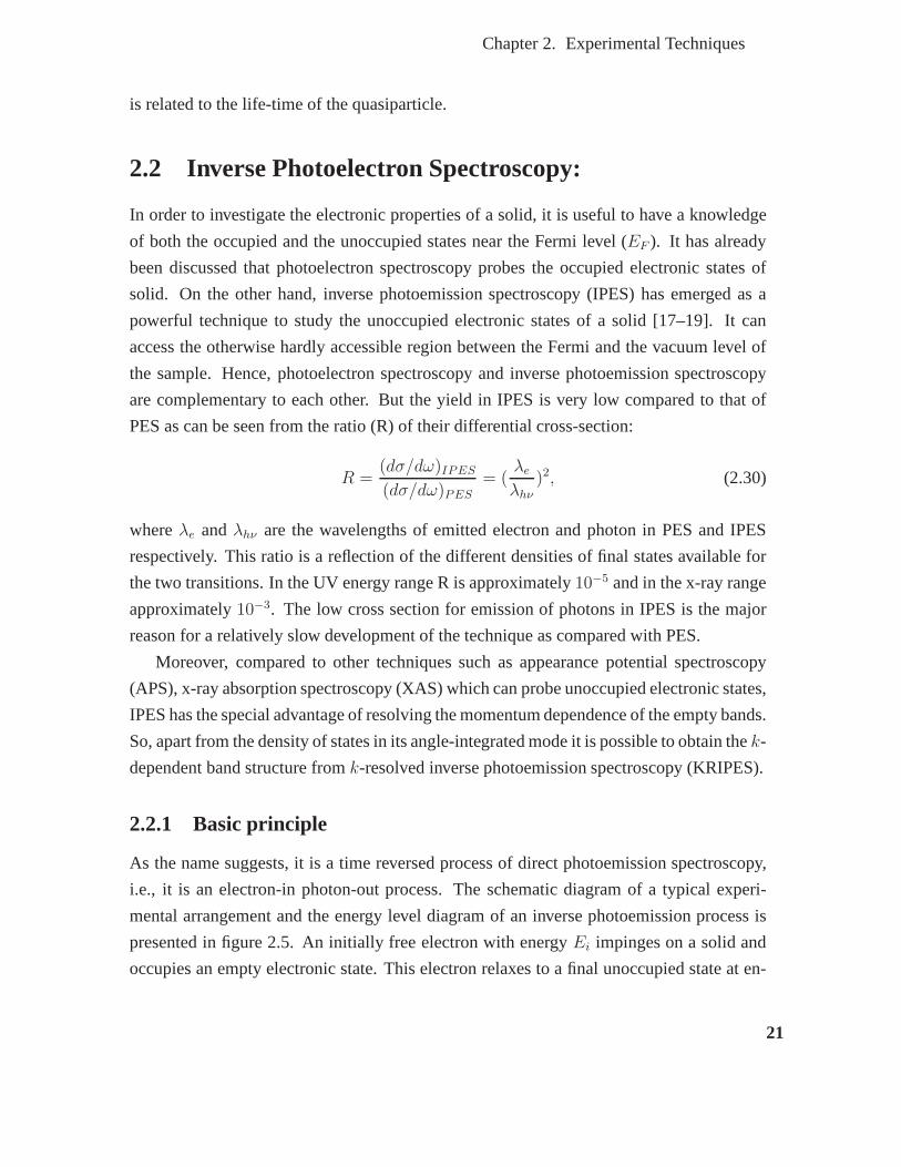
Chapter 2. Experimental Techniques
is related to the life-time of the quasiparticle.
2.2 Inverse Photoelectron Spectroscopy:
In order to investigate the electronic properties of a solid, it is useful to have a knowledge
of both the occupied and the unoccupied states near the Fermilevel (EF ). It has already
been discussed that photoelectron spectroscopy probes theoccupied electronic states of
solid. On the other hand, inverse photoemission spectroscopy (IPES) has emerged as a
powerful technique to study the unoccupied electronic states of a solid [17–19]. It can
access the otherwise hardly accessible region between the Fermi and the vacuum level of
the sample. Hence, photoelectron spectroscopy and inversephotoemission spectroscopy
are complementary to each other. But the yield in IPES is verylow compared to that of
PES as can be seen from the ratio (R) of their differential cross-section:
R =(dσ/dω)IPES
(dσ/dω)PES
= (λe
λhν
)2, (2.30)
whereλe andλhν are the wavelengths of emitted electron and photon in PES andIPES
respectively. This ratio is a reflection of the different densities of final states available for
the two transitions. In the UV energy range R is approximately 10−5 and in the x-ray range
approximately10−3. The low cross section for emission of photons in IPES is the major
reason for a relatively slow development of the technique ascompared with PES.
Moreover, compared to other techniques such as appearance potential spectroscopy
(APS), x-ray absorption spectroscopy (XAS) which can probeunoccupied electronic states,
IPES has the special advantage of resolving the momentum dependence of the empty bands.
So, apart from the density of states in its angle-integratedmode it is possible to obtain thek-
dependent band structure fromk-resolved inverse photoemission spectroscopy (KRIPES).
2.2.1 Basic principle
As the name suggests, it is a time reversed process of direct photoemission spectroscopy,
i.e., it is an electron-in photon-out process. The schematic diagram of a typical experi-
mental arrangement and the energy level diagram of an inverse photoemission process is
presented in figure 2.5. An initially free electron with energy Ei impinges on a solid and
occupies an empty electronic state. This electron relaxes to a final unoccupied state at en-
21
Chapter 2. Experimental Techniques
e−
e b
eam
sample
hν
hνθ
φ
Vacuum level (Ev)
Density of states
k
Ele
ctro
n en
ergy
CaF2window
Inverse photoemissionisochromat spectrum
wor
k fu
nctio
n
(E, )photon detector
Fermi level (E ) F
Figure 2.5: Illustration of inverse photoemission spectroscopy. The typical experimentalarrangement (upper diagram). The energy level diagram of the process (lower diagram). Ifthe measured photon energy is held constant and the incidentelectron beam energy is swept(isochromat mode), the intensity distribution of photon replicates the density of states ofunoccupied electronic states.
ergyEf either through radiative or non-radiative transition. When it undergoes a radiative
transition with the emission of a photon of energyhν, the intensity of the outcoming photon
is measured. This is usually carried out in two ways: (i) the energy of the detected photon
hν is held constant and the spectrum is obtained by sweepingEi (isochromat mode), and
(ii) by fixing the incident electron energy and collecting photons emitted over a range of
energies (parallel detection or spectrograph mode). Analogous to the photoemission one
can measure an intensity distribution of the emitted photonas a function of the final state
energyEf = Ei − hν by varying the initial state energyEi and keeping photon energyhν
constant. Within similar approximation schemes, it turns out that this distribution reflects
the available number of empty final electronic states above the Fermi level. The interaction
Hamiltonian in this case also is same as in direct photoemission (equation 2.14) because
both the processes involve interaction of electron with photon. The sampling of the Bril-
louin zone is determined by the angle of incidence of the electron beam. In the isochromat
22

Chapter 2. Experimental Techniques
mode, the parallel component of the crystal momentumk‖ is given by
k‖ =
√2me
~
√
Ef + hν − φ sin θ, (2.31)
whereθ is the angle of incidence of the electron beam with respect tothe surface normal of
the sample andφ is the work function of the material. In spectrograph modek‖ is given by
k‖ =
√2me
~
√
Ei − φ sin θ, (2.32)
where the initial energyEi is fixed.
2.2.2 Instrumentation
The basic experimental requirement of IPES is an electron source providing a well-defined
beam and a photon detector with limited bandwidth. The photon detectors used in IPES
have fallen into two categories, those which operate in an isochromat or fixed photon en-
ergy mode and those that are tunable, allowing detection at different photon energies. The
KRIPES results, presented in this thesis, were obtained using a band-pass Geiger-Muller
type photon detector with acetone gas filling and CaF2 window (acetone/CaF2) in isochro-
mat mode with a mean photon energy of 9.9eV [20]. A Geiger-Muller counter, as schemat-
ically shown in the upper panel of figure 2.5, consists of a tube closed at one end by a cal-
cium fluoride (CaF2) window and filled with a gas to a certain pressure. The combination
of the transmission properties of the window and the photoionization cross section of the
gas determines the photon energy detected and the bandwidth. A photon with an energy
lower than the cut-off of the window but higher than the ionization potential of the gas will
initiate an electron cascade which is collected by a centralelectrode. For example, the high
energy cut-off of the acetone/CaF2 detector is due to the CaF2 window that does not trans-
mit photons with energy> 10.2eV , while the threshold for the photoionization of acetone
at 9.7eV sets the low energy cut-off. This determines the band-pass function and results
in a mean photon detection energy of 9.9eV with a FWHM of 0.4eV . Thus, 9.9±0.2eV
photons can enter the detector to photoionize acetone.
The typical requirements of electron sources for IPES are a large current at low energies
with a narrow angular spread in the beam. However, the ability to achieve the requirements
of high currents and low energies is restricted by fundamental limits imposed by space-
charge effects: the space-charge-limited current densityat a cathode varies as the three-
23

Chapter 2. Experimental Techniques
halves power of the extraction voltage and inversely as the square of the cathode-anode
distance. A Stoffel-Johnson type [21] electron source was used in our experiment. This is
chosen because it has less space-charge effect and high beamcurrent.
2.3 Resonance Photoemission Spectroscopy (ResPES)
Resonance photoemission is one of the not so common photoemission techniques and has
been used for the investigation of valence band features in transition-metal oxide com-
pounds. Before going into the details of this technique, a brief description of another
technique called X-ray absorption spectroscopy (XAS) willbe given because to carry out
a resonance photoemission experiment, XAS is a prerequisite in order to select the photon
energy at which the resonance phenomenon will occur.
2.3.1 X-ray Absorption Spectroscopy
X-ray absorption spectroscopy (XAS) is a very powerful technique in the investigation of
the unoccupied states as well as the local geometrical structure of a material near an atom.
In this method a monochromatic beam of X-rays enters into thesolid and may get scattered
or absorbed. In the absorption process a core electron is excited to an unoccupied state or to
continuum depending on the energy of incident X-rays. Fig 2.6 shows the schematic of X-
ray absorption process. When the energy of an incident X-rayphoton exceeds the binding
energy of a particular core level, the photon can be absorbed, and the core electron is
excited to an unoccupied state, leaving a hole in the core-level. Such a core hole may decay
through X-ray fluorescence or Auger electron emission. The incident photon intensityI0
and transmitted photon intensityI are related asI = I0 exp−µx with x being the sample
thickness andµ is called the absorption coefficient.µ is a function of sample densityρ,
atomic numberZ, atomic massA and energyE of incident X-rays. In XAS, the absorption
coefficientµ is measured as a function of energyE. A typical XAS spectrum has several
parts. As the photon energy equals with the binding energy ofa core level, there is a
sharp rise inµ which is known as edge and the energy is referred as absorption threshold.
The spectral region of a few tens of eV near the threshold is known as near-edge X-ray
absorption fine structure (NEXAFS) and the region (upto∼ 100 eV) beyond NEXAFS
is known as extended X-ray absorption fine structure (EXAFS). Using X-ray absorption
spectroscopy we determined the threshold energy of Mn2p-3dtransition in a manganite
24

Chapter 2. Experimental Techniques
Figure 2.6: A schematic diagram of the X-ray absorption process: an electron is excitedfrom the core level (CL) to the unoccupied states in conduction bands (CB) by absorbinga photon with energy hν, leaving a hole in the core level. Such an electron-hole pairmaydecay through either X-ray fluorescence or emission of Augerelectrons.
sample.
There are several techniques for measuring the XAS. The mostdirect method is to mea-
sure the absorption of the sample by monitoring the incomingand the transmitted flux. But
this method requires the sample thickness to be very small incase of a large absorption
coefficient. By monitoring secondary processes like X-ray fluorescence and Auger elec-
tron emission, the absorption can also be measured. A more practical way to measure the
absorption is the total-electron yield (TEY) mode, in whichall electrons emitted from the
sample are collected by an analyzer. The XAS data presented in this thesis were collected
in the total electron yield mode.
2.3.2 ResPES
In this spectroscopy one excites electrons with photons of energyhν very near to the ab-
sorption threshold of a core level. The direct photoemission of valence band electrons can
then interfere with the Auger CVV-electrons that are emitted in a Super Koster-Kronig
25

Chapter 2. Experimental Techniques
process. The intensity in the valence band features for which the direct photoemission pro-
cess and the Auger emission overlap is given as a function of the photon energyhν by the
so-called Fano lineshape
N(hν) ≃ (ǫ + q)2
(ǫ2 + 1); ǫ =
(hν − hνj)
∆(hνj)/2(2.33)
wherehνj is a photon energy equal to the binding energy of a core level (near which the
resonance is investigated),q is a parameter for the particular core level and∆(hνj) is the
full width at half maxima (FWHM) of that core level.
Figure 2.7: A schematic diagram for a resonant photoemission process for 3d transitionmetal compounds.
Fig. 2.7 illustrates the resonant photoemission process ofa 3d transition-metal com-
pound at the2p-3d threshold. In the2p-3d threshold, in addition to the direct photoemis-
sion process (process 1 in the Fig. 2.7): 3dn + hν → 3dn−1 + e−, the following atomic
process (process 2 in Fig 2.7) takes place. 3dn → c3dn+1 → 3dn−1 + e−, where cdenotes
a hole in the2p core level. The first step of such a process is the absorption of a photon,
leading to a transition from the2p core level to the3d valence band and leaving an inter-
mediate hole state in the2p core level. The second step is a two-electron Koster-Kronig
decay of the intermediate state involving emission of an Auger electron. The above two
indistinguishable processes are added coherently due to quantum interference, leading to
26

Chapter 2. Experimental Techniques
an intensity modulation at the2p-3d threshold.
2.4 Instrumentation
The photoemission spectrometric system in our laboratory consists of two OMICRON
ultra-high vacuum (UHV) chambers, the main chamber or analysis chamber and a sam-
ple preparation chamber. For quick sample loading without breaking the UHV conditions
in preparation and analysis chambers a small load lock chamber is attached with the prepa-
ration chamber. Further, the sample preparation chamber isequipped with a four-axes ma-
nipulator, a diamond file, a sample heater, an evaporator andan Ar ion sputter gun. Samples
from the preparation chamber are transferred by using a magnetically coupled transfer rod.
Theµ metal main chamber can protect the photoemitted electrons from earth’s magnetic
field and any stray magnetic field. The analysis chamber is equipped with the sources of
energetic photons (X-ray and VUV-light), the hemispherical electron energy analysers (EA
125 and AR 65), four-axes cryo-manipulator and low energy electron diffraction (LEED)
unit to check sample surface orientation. The working principle of a few of the important
components are discussed below.
2.4.1 Gas Discharge Lamp
The VUV source can be operated with various discharge gases like helium, neon, argon,
krypton, xenon or hydrogen. The operation of the lamp is based on the principle of a cold
cathode capillary discharge [30]. The lamp is water cooled in order to allow for high dis-
charge current and to reduce electrode degradation resulting in prolonged service intervals.
There is a windowless direct sight connection between the discharge area and target. The
ignition potential is an order of magnitude higher than the operating potential needed to
maintain a continuous discharge. The nature and intensity of the radiation are strongly
dependent on gas pressure and discharge current. There are two modes of functioning,
namely, lines of neutral atoms (HeI, NeI etc.) and lines of singly charged ions (HeII, NeII
etc.). Here, in our ARUPS Laboratory we use a discharge lamp using He or Ne for high
resolution studies of the valence band and the near Fermi level (EF ) features.
In the VUV discharge lamp, a high dc voltage (∼ 500 V) is applied across a cell con-
taining an inert gas e.g., helium or neon. This will cause an electrical discharge in the gas in
which atoms go into an excited state and subsequently the excited states decay very fast by
27

Chapter 2. Experimental Techniques
emitting photons with an energy equal to the energy difference between the excited states
and the ground states. In the case of helium, two groups of radiation are present: the first
one originates from the decay of excited neutral helium atoms i.e., He 1s 2p→ He1s2 (α),
He 1s 3p→ He 1s2 (β), He 1s 4p→ He 1s2 (γ), He 1s 5p→ He 1s2 (δ), and the second
one from the decay of singly ionized helium atoms, i.e., He+ 2p→ He+ 1s (α), He+ 3p→He+ 1s (β), He+ 4p→ He+ 1s (γ), He+ 5p→ He+ 1s (δ). They are labeled as He I (α, β,
γ andδ) and He II (α, β, γ andδ) respectively. Theα lines are the strongest ones and occur
at21.22 eV and40.81 eV for He I and He II respectively. The relative intensities of He I α
and He IIα depend on the conditions of the discharge, particularly thelamp pressure. The
amount of He II radiation is normally very small but can be increased by decreasing the
lamp pressure. The typical discharge condition for He I are the following:
Inert gas used Discharge voltage Discharge current Lamp pressure
(Volt) (mA) (mbar)
Helium ∼ 500 80 ∼ 8.7 × 10−01
1s 2p→ 1s2 (He I α)
In order to produce a narrow beam the discharge is confined in anarrow quartz capillary.
A capillary is mounted at the output stage of the lamp to direct the light onto the sample
target. The total photon intensity that is transferred through the capillary to the sample
target is proportional to the cross sectional area of the inner bore of the capillary. Due to
lack of proper window material in the UV range, two stages of differential pumping are
employed to maintain the chamber in UHV while providing a stable pressure in the lamp.
At the first stage, the discharge region is pumped down to a pressure of∼ 10−2 mbar using
a rotary pump, whereas for the second stage, a turbomolecular pump is employed to further
reduce the He gas pressure before the main vacuum chamber.
2.4.2 X-ray source
We used DAR 400 X-ray source from OMICRON. It is a twin anode (Mg Kα (1253.6 eV)
Al K α (1486.6 eV)) X-ray source. Electrons are extracted from a hot filament and focused
to bombard the selected surface of an anode at high positive potential. The excited core
28

Chapter 2. Experimental Techniques
level electrons emit characteristic X-rays when they de-excite to a lower energy level. The
anode is water cooled to prevent the aluminium or magnesium surfaces from evaporating.
X-rays generated at the surface of the anode pass through a thin aluminium window to the
sample under study. The aluminium window acts as a partial vacuum barrier between the
source and the sample region.
2.4.3 Synchrotron Radiation
Frequencies generated in Synchrotron radiation (SR) covers almost the entire range of elec-
tromagnetic spectrum. Hence, Synchrotron radiation sources are widely used in PES ex-
periments. It is well known that accelerated or deceleratedcharged particles emit elec-
tromagnetic radiation. Based on this principle, Synchrotron radiation is produced from
the relativistic electrons, which are guided in a polygon-shaped vacuum tube (called stor-
age ring) by applying a centripetal acceleration. This centripetal acceleration is caused by
strong magnets arranged on the corners of the polygon. The electrons are emitted from
a cathode and accelerated linearly outside the ring up to several MeV. Then the electrons
are inserted into the ring and the bending magnets deflect them. At this stage the electrons
emit synchrotron radiation tangential to their trajectory. The energy loss of the electrons
due to emission of radiation is compensated by allowing the electrons to pass through
radio-frequency cavity. In the present days, insertion devices such as wigglers and undu-
lators which employ periodic magnetic fields to produce radiation with no net deflection
of the beam are used to obtain much brighter radiation. Finally a beamline takes the ra-
diation from the ring to the experimental stations. Compared to discrete resonance lines
obtained from laboratory source synchrotron source provides several advantages, e.g., its
high intensity photon beam allows rapid experiments and highly collimated (due to spatial
coherence) photon beam generated by a small divergence allows one to study very small
size sample.
The resonance photoemission and x-ray absorption spectroscopy presented in this work
were carried out using BACH beamline at Elettra synchrotronlight laboratory, Trieste,
Italy. BACH beamline employs undulators to enhance the intensity of emitted radiation.
It works in the UV-soft X-ray photon energy range (35-1600 eV) with selectable light
polarizations. It is equipped with four spherical gratings(SG1, SG2, SG3 and SG4) to
select photons in different energy ranges.
29
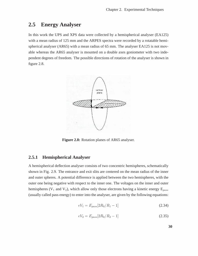
Chapter 2. Experimental Techniques
2.5 Energy Analyser
In this work the UPS and XPS data were collected by a hemispherical analyser (EA125)
with a mean radius of 125 mm and the ARPES spectra were recorded by a rotatable hemi-
spherical analyser (AR65) with a mean radius of 65 mm. The analyser EA125 is not mov-
able whereas the AR65 analyser is mounted on a double axes goniometer with two inde-
pendent degrees of freedom. The possible directions of rotation of the analyser is shown in
figure 2.8.
Figure 2.8: Rotation planes of AR65 analyser.
2.5.1 Hemispherical Analyser
A hemispherical deflection analyser consists of two concentric hemispheres, schematically
shown in Fig. 2.9. The entrance and exit slits are centered onthe mean radius of the inner
and outer spheres. A potential difference is applied between the two hemispheres, with the
outer one being negative with respect to the inner one. The voltages on the inner and outer
hemispheres (V1 and V2), which allow only those electrons having a kinetic energy Epass
(usually called pass energy) to enter into the analyser, aregiven by the following equations:
eV1 = Epass[2R0/R1 − 1] (2.34)
eV2 = Epass[2R0/R2 − 1] (2.35)
30

Chapter 2. Experimental Techniques
Figure 2.9: A schematic diagram of hemispherical analyser.
where R1 and R2 are the radii of the inner and outer spheres, respectively with respect to a
common centre, and R0 denotes the mean radius of the two spheres with R0 = (R1 + R2)/2.
The theoretical energy resolution of the analyser∆E is approximately expressed as [28]
∆E = Epass[d/2R0 + α2/4] (2.36)
whered is the slit width (entrance slit) andα (in radian unit) is the acceptance angle of the
analyser. In practice the energy resolution can be varied bychanging the pass energy and
slit width.
2.5.2 Electron Lens System
The electron lens is a multi-element electrostatic lens fitted at the entrance to the analyser.
The purpose of the lens is to collect electrons from a larger solid angle and to vary the
energy of the beam to the pass energy of the analyser. The resolution obtainable with the
hemispherical analyser can be significantly increased by reducing the pass energy of the
analysed electrons. An electron lens typically consists oftwo or more cylinders, which
are held at different potentials. The electric field that exists between the elements acts
31

Chapter 2. Experimental Techniques
upon the electrons that pass through it. In cylindrical lenses, the adjacent cylinders are
kept at different potentials and focusing takes place. The simplest practical lens consists of
two aligned cylinders at different potentials. However, byemploying a third element it is
possible to accelerate or retard electrons by varying amounts.
2.5.3 Single Channel Detector
The photoelectrons in a PES experiment is counted using a channeltron. A channeltron is
an electron multiplier made up of a small curved glass tube, the inside wall being coated
with a high resistance material. A high voltage is applied along the tube. When a high
energy particle enters the low potential end of the tube it collides with the wall, ejecting
secondary electrons. These secondary electrons are then accelerated down the tube, making
further collisions with the curved wall; each collision generates more and more electrons
in an avalanche, resulting in a large electron cloud at the other end of the tube. Thus,
from an input of one electron the channeltron respond by producing an output pulse with a
typical gain of 108 [28]. The output can either be measured by a ratemeter or a computer.
The data-taking capacity can be enhanced by using a multichannel detector, which consists
essentially of a microchannel plate or several channeltrons to perform parallel detection.
We have used a single channel detector to detect the photoelectrons passing through the
hemispherical deflector.
Figure 2.10: A schematic diagram of electron amplification in a channeltron.
32

Chapter 2. Experimental Techniques
2.5.4 Pulse Counting Operation
In an electron spectrometer, electrons which arrive at the input of the channeltron detector
generate secondary electrons which are then accelerated down the channeltron by a positive
voltage bias (+2 kV to +3 kV at the output). These electrons strike the channeltron wall
producing additional electrons progressively down the channeltron to the output where
between 107 to 108 electrons arrive (fig. 2.10).
2.5.5 Channeltron Operating Plateau
Co
un
t R
ate
Desired Operating Voltage
Maximum Operating Voltage
Operating region
Plateau
Applied Voltage (kV)
Ionic feedback region
~ 2.1 kV ~ 2.8 kV
Figure 2.11: A plateau curve of a channeltron.
As the voltage applied to a channeltron is increased, the gain increases and the output
pulse height increases. As more and more output pulses exceed the threshold set in the
preamplifier, the observed count rate increases. When the gain is large enough for the
smallest pulses in the distribution to exceed the threshold, a plateau is reached and no
further increase in count rate is observed with higher voltages as shown in figure 2.11. At
very high voltages, the observed count rate again increasesdue to the feedback of positive
ions generated within the channeltron. This should always be avoided as the observed
pulses do not result from an input and operating channeltrons in this condition considerably
reduces their lifetime.
33

Chapter 2. Experimental Techniques
The onset of the plateau is reached at approximately2 kV for new channeltrons and this
slowly increases as the channeltron ages. The desired operating voltage is approximately
100 V above the onset of the plateau. The electron pulse is then routed to a preamplifier
which filters out the system noise using a high speed threshold comparator circuit. The
electrical signal is converted to an optical signal which istransmitted to the receiver unit
via an optical fiber link. The receiver unit converts the optical signal to a digital electronic
pulse which is then counted by the computer. The optical linkisolates the pulse counting
system, usually a computer, from the spectrometer and low noise data levels.
2.5.6 Low Energy Electron Diffraction (LEED) unit
In addition to the gas discharge lamp and two electron spectrometers EA125 and AR65,
the main chamber is also equipped with a Low Energy Electron Diffraction (LEED) appa-
ratus which is used to determine the orientation of crystal surface. The LEED experiment
uses a beam of electrons of a well-defined low energy (typically within 20 -200 eV) inci-
dent normally on the sample. Since the de Broglie wavelengthassociated with low energy
electron is comparable to the lattice constant of a crystal,its diffraction can give informa-
tion regarding the geometrical structure of the crystal andas the energy is quite low it is
very much surface sensitive. The sample under study must be asingle crystal with a well-
ordered surface structure in order to generate a back- scattered electron diffraction pattern.
For a polycrystal it will give a diffused circular pattern. Atypical experimental set-up
is shown in figure 2.12. Only the elastically-scattered electrons contribute to the diffrac-
tion pattern. The lower energy (secondary) electrons are removed by energy-filtering grids
placed in front of the fluorescent screen that is employed to display the pattern.
2.5.7 Sample Surface Preparation
It has already been discussed that the PES experiment is a highly surface sensitive tech-
nique [29]. In order to get the spectra from clean surfaces, vacuum better than 10−10 mbar
is mandatory for VUV-PES experiments. This makes the preparation and preservation of a
clean sample surface essential to PES measurement. Among the surface preparation tech-
niques that have been used, in situ scraping and in situ cleaving are the safest. Here we have
used in situ cleaving for graphite samples, i.e., single crystal graphite and HOPG. The sam-
ples were cleaved by using post technique inside the preparation chamber. The transition
metal oxide samples, i.e., Bi1−xPbxFeO3 and Sm0.1Ca0.9−xSrxMnO3, were scraped insitu
34
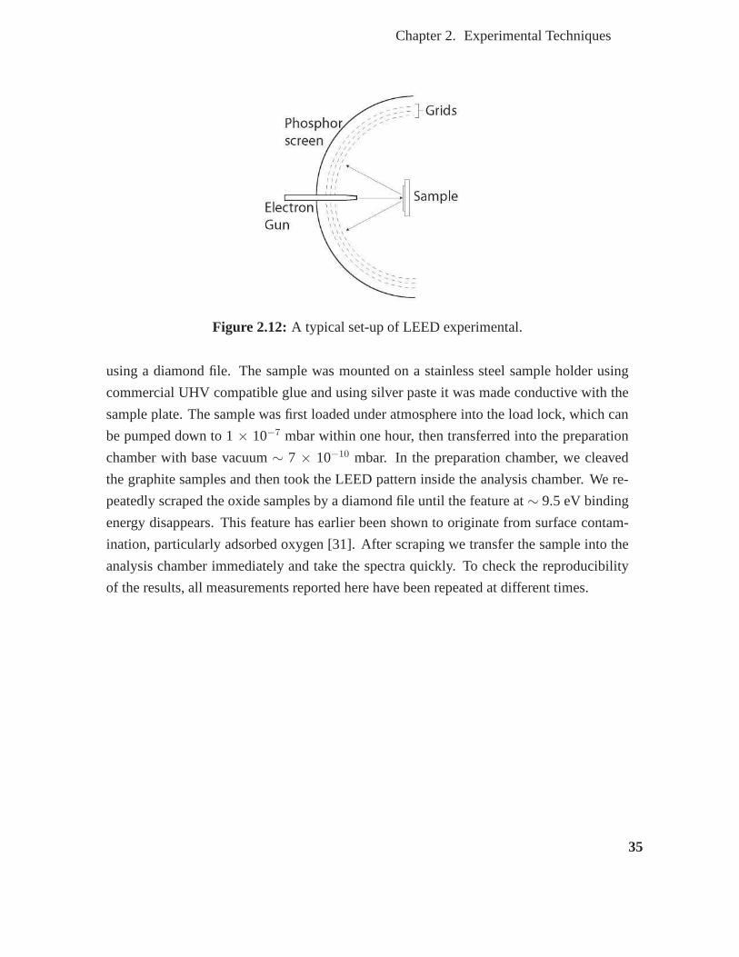
Chapter 2. Experimental Techniques
Figure 2.12: A typical set-up of LEED experimental.
using a diamond file. The sample was mounted on a stainless steel sample holder using
commercial UHV compatible glue and using silver paste it wasmade conductive with the
sample plate. The sample was first loaded under atmosphere into the load lock, which can
be pumped down to 1× 10⁻⁷ mbar within one hour, then transferred into the preparation
chamber with base vacuum∼ 7 × 10⁻¹⁰ mbar. In the preparation chamber, we cleaved
the graphite samples and then took the LEED pattern inside the analysis chamber. We re-
peatedly scraped the oxide samples by a diamond file until thefeature at∼ 9.5 eV binding
energy disappears. This feature has earlier been shown to originate from surface contam-
ination, particularly adsorbed oxygen [31]. After scraping we transfer the sample into the
analysis chamber immediately and take the spectra quickly.To check the reproducibility
of the results, all measurements reported here have been repeated at different times.
35

Bibliography
[1] H. Hertz; Ann. Phys.17, 983 (1887).
[2] J. J. Thomson; Phil. Mag.48, 547 (1899).
[3] P. Lenard; Ann. Physik2, 359 (1900).
[4] A. Einstein; Ann. Phys.31, 132 (1905).
[5] C. N. Berglund and W. E Spicer, Phys. Rev.136, A1044 (1964)
[6] G. W. Gobeli, E. O. Kane, and F. G. Allen, Phys. Rev. Lett.12, 94 (1964)
[7] E. O. Kane, Phys. Rev. Lett.12, 97 (1964)
[8] N. V. Smith and L.F. Mattheiss. Phys. Rev. B,9, 1341 (1974).
[9] N. V. Smith. Phys. Rev. B,9, 1365 (1974).
[10] N. V. Smith, M. M. Traum, and F. J. DiSalvo. Solid State Comm.15. 211 (1974).
[11] M. M. Traum, N. V. Smith and F.J. DiSalvo. Phys. Rev. Lett. 32, 1241 (1974).
[12] T. Kiss, F. Kanetaka, T. Yokoya, T. Shimojima, K. Kanai,S. Shin, Y. Onuki, T. To-
gashi, C. Zhang, C. T. Chen and S. Watanabe. Phys. Rev. Lett.94, 057001 (2005).
[13] C. N. Berglund and W. E Spicer, Phys. Rev.136, A1030 (1964)
[14] H. Y. Fan; Phys. Rev.68, 43 (1945).
[15] H. Mayer and H. Thomas; Z. Phys.147, 419 (1957).
[16] H. Puff; Phys. Stat. Sol.1, 636 (1961).
[17] Volker Dose, Progress In Surface Science,13, 225-284 (1983)
[18] Neville V Smith, Rep. Prog. Phys.51, 1227-1294 (1988)
[19] P. D. Johnson, S. L. Hulbert, Rev. Sci. lnstrum.61, 2277 (1990)
[20] S. Banik, A. K. Shukla, and S. R. Barman, Rev. Sci. lnstrum 76, 066102 (2005)
[21] N. G. Stoffel and P. D. Johnson, Nucl. Inst. & Meth. A234, 230 (1985)
36
Bibliography
[22] G. D. Mahan; Phys. Rev. B2, 4334 (1970)
[23] C. Caroli, D. Lederer-Rosenblatt, B. Roulett, and D. Saint James; Phys. Rev. B8,
4552 (1973)
[24] P. J. Feibelman and D. E. Eastman; Phys. Rev. B10, 4932 (1974)
[25] G. Jezequel and I. Pollini: Phys. Rev. B41, 1327 (1990)
[26] L. Hedin and S. Lundqvist, in Solid State Physics, edited by F. Seitz, D. Turnbull, and
H. Ehrenreich, (Academic Press, New York, 1969), Vol.23
[27] S. G. Louie, in Angle-resolved Photoemission, edited by S. D. Kevan, (Elsevier, Am-
sterdam, 1992), Vol.74
[28] Omicron Instruction Manual for HA Analyser.
[29] D. A. Shirley; in Photoemission in Solids I, edited by M.Cardona and L. Ley,
(Springer Verlag, Berlin, 1978) Vol26, p. 193
[30] G Schönhense and U Heinzmann, J. Phys. E: Sci. Instrum.16, 74 (1983)
[31] D. D. Sarma, N. Shanthi, S. R. Krishnakumar, T. Saitoh, T. Mizokawa, A. Sekiyama,
K. Kobayashi, A. Fujimori, E. Weschke, R. Meier, G. Kaindl, Y. Takeda and M.
Takano, Phys. Rev. B53, 6873 (1996)
37

3Tight Binding Calculations of Graphene,
Bilayer Graphene and Graphite
3.1 Introduction
In this chapter we describe our tight binding band structurecalculations of three graphitic
systems, namely, graphene, bilayer graphene and graphite as in the next chapter we will be
presenting valence and conduction band mapping of graphiteusing ARPES and KRIPES.
Though we have done experiment only on graphite, the band calculation has been initiated
with graphene, the two dimensional approximation of graphite, then developed for bilayer
graphene, a system more close to graphite in reality, and finally extended up to three dimen-
sional graphite within similar formalism because it gives some sort of completeness as well
as helps to build up an insight of how the electronic dispersion evolves with the dimension-
ality of a system. To calculate the bands, tight binding scheme has been chosen because the
pz electrons, which are almost localized in space, play the fundamental role in determining
the electronic behaviours in these materials. In the subsequent paragraphs we will intro-
duce the above mentioned systems individually and discuss how far these materials have
been exploited using tight binding method.
Graphene is a single sheet of atomic thickness with carbon atoms arranged hexagonally.
Though it is an ideal two dimensional material of theoretical interest and one of the earliest
material on which tight binding band structure calculationwas done [2, 3], it has triggered
recently a lot of interest including the reinvestigation ofmany earlier results since its ex-
perimental discovery in 2004 [4], particularly, a large no of tight binding band calculations
have been performed with nearest neighbour hopping but without overlap integral correc-
38

Chapter 3. Tight Binding Calculations of Graphene, BilayerGraphene and Graphite
tion [1–3, 5–9]. Some calculations have considered the overlap integral correction [2, 8],
out of these only few calculations are there which take care of second and third nearest
neighbours along with overlap integral corrections [1, 9].It is noticed that the first nearest
neighbour hopping integral (γ0) lies around 2.5eV-3.0eV when tight binding band is fitted
with first principle calculation or experimental data [1, 6,8] near theK point of the bril-
louin zone of graphene, but interestingly, when one tries tohave a good agreement of the
tight binding band over the whole brillouin zone by including up to third nearest neighbour
hoppings and overlap integrals, the tight binding parameters are considered as merely fit-
ting parameters, not as physical entities [1] i.e., the values of parameters do not decrease
consistently as one moves towards second and third nearest neighbours. In present work
we have fitted our tight binding band with first principle datawith the objective to get a set
of parameters which is free from the above discrepancy and found out a set which gives
good matching with the first principle data over the whole brillouin zone. Here we have
also calculated the density of states with second and third nearest neighbours.
Bilayer graphene is a system of two stacked hexagonal graphene sheets. Among all the
carbon based materials of recent interest, bilayer graphene is of much importance because
this is the only two dimensional material in which the band gap between valence and con-
duction bands can be controlled by applying an external electric field perpendicular to the
layers [9–14] or by chemical doping of one of the layers [15].This makes it a potential
candidate for future application in nanoelectronics. There has been a significant amount of
effort to study the band structure of bilayer graphene [5, 9,15–17]. Regarding this the ma-
jor concern was to see how the linear dispersion near theK point in single layer graphene
gets modified in presence of interlayer coupling in bilayer graphene. It is now well estab-
lished that even the slightest presence of the interlayer coupling kills the linearity of the
dispersion of monolayer graphene and converts it to a parabolic one for the Bernal stacked
bilayer graphene. Moreover, most of the studies have talkedabout the symmetric nature
of the valence and conduction bands of bilayer graphene. Only very recently there have
been reports [17–19] regarding asymmetry between the valence and conduction bands in
this system. In the present work on bilayer graphene we have investigated some parameters
which also contribute appreciably towards asymmetry in thebands of this system. While
the existing literature mostly discusses the effect of interlayer coupling in bands of bilayer
graphene and in graphite [20], we report here about the asymmetry in band structure of
bilayer graphene which arises due to the inclusion of in-plane and interplane nearest neigh-
bour overlap integrals (s0 ands′
1) in the tight binding band structure calculation because
39

Chapter 3. Tight Binding Calculations of Graphene, BilayerGraphene and Graphite
we have noticed that the presence of nearest neighbour overlap integral (s0) gives quite a
bit of asymmetry in the band structure of monolayer graphene[2,8]. We have also studied
the effects of in-plane next nearest neighbour and next to next nearest neighbour hopping
energies (γ1 andγ2) along with the corresponding overlap integrals (s1 ands2) on the band
structure of this system in line with the work on single layergraphene [1]. The in-plane
parameters used here were determined by comparing the tightbinding bands of single layer
graphene with the first principle results, by emphasizing the fact that the magnitudes of the
parameters should decrease with increasing distance (e.g., γ0 > γ1 > γ2 ands0 > s1 > s2
) as has been mentioned in the previous paragraph.
Graphite is a weakly three dimensional system of infinite stack of graphene sheets with
interlayer distance much larger than in-plane interatomicdistance. In nature graphite exists
with various stacking sequences, namely AA, AB (Bernal stacking) and ABC among which
AB stacked graphite is most abundant. In this work, utilizing the same tight binding in-
plane coupling parameters for single layer graphene and theinterlayer coupling parameters
for bilayer graphene, we have calculated the band structureof AB stacked graphite in the
way similar to that of bilayer graphene and discussed the effect of these parameters on the
energy dispersions along different high symmetry directions, particularly near theK and
H points.
3.2 Geometrical structure
Since the geometrical structure of a material plays a crucial role in determining its elec-
tronic dispersion, it is important to look at the details of the crystal structure. Here we
describe the structures of graphene, bilayer graphene and graphite. An ideal graphene
sheet consists of a regular hexagonal arrangement of carbonatoms in two dimension as
shown in fig. 3.1. It consists of two inequivalent (with respect to orientations of bonds)
triangular sublattices called A-sublattice and B-sublattice. The unit cell contains one A
and one B type of carbon atoms contributed by respective sublattices. Each carbon atom
has three nearest neighbours coming from the other sublattice, six next nearest neighbours
from the same sublattice and three next to next nearest neighbours from the other sublat-
tice. a0 (1.42 A) is the nearest neighbour lattice distance. In the figure,~a1 and~a2 are
the unit vectors with magnitudea =√
3a0 i.e., 2.46A. With respect toA0 atom the
coordinates of the first neighbours (B1i, i = 1, 2, 3); second neighbours (A2i, i = 1, ...6)
and third neighbours (B3i, i = 1, 2, 3) are(
a/√
3, 0)
,(
−a/2√
3,−a/2)
,(
−a/2√
3, a/2)
;
40

Chapter 3. Tight Binding Calculations of Graphene, BilayerGraphene and Graphite
(0, a) ,(√
3a/2, a/2)
,(√
3a/2,−a/2)
,
(0,−a) ,(
−√
3a/2,−a/2)
,(
−√
3a/2, a/2)
and(
a/√
3, a)
,(
a/√
3,−a)
,(
−2a/√
3, 0)
re-
spectively.
A
A
A
A
A
A
A
B
B
B
B
011
1
1
2
2
2
2
2
2
2
2
3
3
3
3
33
1
2
1
4
6
5
a
a
a0
2
1B
B
Figure 3.1: Structure of graphene. The structure with black circles forms the A-sublatticeand that with empty circles gives B-sublattice.~a1 and~a2 are the unit vectors.
Bilayer graphene is a coupled system of two monolayers of graphene with usually an
AB-stacking fashion of the layers, i.e., the atoms in one layer are not just on top of the
corresponding atoms in the other layer, rather the arrangement is such that if one layer
is projected on the other, the A-type (say) atoms coincide with the A-type atoms but the
B-type atoms come at the center of the hexagons of the other layer [16]. So A and B
type atoms can not be treated as chemically equivalent carbon atoms as they belong to two
different chemical environments. This site energy difference between two atoms in two
different sublattices in the same layer is defined here as theasymmetry energy∆. Since
its value is very small (∼ 18 meV) [18], these two atoms are usually treated as chemically
equivalent. The structure of AB stacked bilayer graphene and its brillouin zone are shown
in figure (3.2). The distance between two atoms in a layer is the same as graphene and
the interlayer separation is 3.35A. The brillouin zone of bilayer graphene is also same
as that of single layer graphene because it does not have periodicity along z-direction.
Bilayer graphene unit cell contains four atoms. The relevant hopping parameters, i.e.,
41

Chapter 3. Tight Binding Calculations of Graphene, BilayerGraphene and Graphite
nearest neighbour in-plane coupling energy (γ0), nearest neighbour interplane coupling
energy (γ′
1), next nearest neighbour in-plane coupling energy (γ1) and next to next nearest
neighbour in-plane coupling energy (γ2) have also been shown in the figure.
A B
b 2
b1
M
K
Γ
(a)
a 1
a 2
γ0
γ
(b)
γ
γ
12
’1
Figure 3.2: (a) Structure of bilayer graphene with unit vectors~a1, ~a2; the intralayer near-est neighbour coupling energy (γ0), interlayer nearest neighbour coupling energy (γ
′
1), in-tralayer next nearest neighbour coupling energy (γ1) and next to next nearest neighbourcoupling energy (γ2). (b) Brillouin zone of single layer and bilayer graphene with unitvectors~b1,~b2 and the high symmetry directions.
The structure of graphite is an infinite sequence of AB-stacked graphene layers where
the interlayer atomic distance is much larger compared to the intralayer atomic distance
similar to bilayer graphene. The only difference with a bilayer graphene is that it has
periodicity along the third direction also leading to a three dimensional brillouin zone.
Also, in principle, the value of the asymmetric energy parameter∆ should be different in
this case.
3.3 Electronic structure of a hexagonal sheet of carbon
atoms
Since hexagonal array of carbon atoms, i.e., graphene is thebuilding block of bilayer
graphene and graphite, it will be relevant to discuss first the basics of electronic config-
uration of the carbon atoms in graphene. Carbon atom has six electrons with the electronic
configuration1s22s22p2. 2s and 2p levels of carbon atom can mix up with each other and
give rise to various hybridized orbitals depending on the proportionality of s and p orbitals.
Graphene hassp2 hybridization: 2s orbital overlaps with2px and2py orbitals and generates
three new in-planesp2 orbitals each having one electron. The2pz orbital remains unaltered
and becomes singly occupied. Due to overlap ofsp2 orbitals of adjacent carbon atoms
42

Chapter 3. Tight Binding Calculations of Graphene, BilayerGraphene and Graphite
strongσ (bonding) andσ∗ (antibonding) bonds are formed. The bondingσ bonds, lying in
a plane, make an angle of120◦ with each other and is at the root of hexagonal planar struc-
ture of graphene.pz orbitals being perpendicular to the plane overlap in a sidewise fashion
and giveπ (bonding) andπ∗ (antibonding) bonds.sp2 orbitals with a lower binding energy
compared to1s (core level) are designated as semi core levels andpz orbitals having lowest
binding energy are the valence levels. Overlapping ofpz energy levels gives the valence
band (bondingπ band) and conduction band (antibondingπ∗ band) in graphene. Thus, we
see that while the structure of graphene is because ofσ bonds, theπ band is responsible for
the electronic properties of graphene and hence, as far as electronic properties of graphene
are concerned, emphasis is given only onπ bands. Since thepz orbitals overlap in a side-
wise manner, the corresponding coupling is weaker comparedto that ofσ bonds (wheresp2
orbitals overlap face to face). Therefore thepz orbitals essentially retain their atomic char-
acter. Hence, to describe the electronic structure of graphene as well as of bilayer graphene
and graphite, tight binding model could be a good choice.
3.3.1 Tight binding band of graphene
In this subsection tight binding bands of graphene have beenreproduced including up to
third nearest neighbour hopping of electrons and overlap integral corrections with focus
on the point to find out tight binding parameters which are notjust fitting parameters but
they have physical significance. The results have been compared with existing literature [1].
The key equations are shown here for the different cases of nearest neighbours, next nearest
neighbours and next to next nearest neighbours and the details of the calculations are given
in the last section of this chapter. Since there are two atomsper unit cell coming from two
sublattices, the total wave function can be written as
Ψk(r) = CAΨkA + CBΨk
B, where (3.1)
ΨkA/B(r) =
(
1/√
N)
∑
A/B
ei~k.~rA/BΦA/B(r − rA/B) (3.2)
are the tight binding Bloch wave functions from A and B sublattices. Here, N is the number
of unit cells in the crystal,CA andCB are contributions coming from A and B sublattices
respectively,Φ′
s are2pz atomic orbitals,k is crystal momentum andrA andrB are the posi-
tions of A and B atoms respectively with respect to a chosen origin. If H is the Hamiltonian
43

Chapter 3. Tight Binding Calculations of Graphene, BilayerGraphene and Graphite
andE(k) the eigenvalue then
HΨk(r) = E(k)Ψk(r), (3.3)
which leads to the secular equation
∣
∣
∣
∣
∣
HAA − E(k)SAA HAB − E(k)SAB
H∗AB − E(k)S∗
AB HBB − E(k)SAA
∣
∣
∣
∣
∣
= 0 (3.4)
whereHxy =∫
Ψ∗kx (r)HΨk
y(r)d~r = H∗yx andSxy =
∫
Ψ∗kx (r)Ψk
y(r)d~r = S∗yx. The indices
x andy represent both A and B. Since two sublattices are equivalent, HAA = HBB and
SAA = SBB . The general dispersion relation follows as
E±(k) =[
(2E0 − E1) ±√
(E1 − 2E0)2 − 4E1E2
]
/2E3, (3.5)
whereSAAHAA = E0, HABS∗AB + H∗
ABSAB = E1, H2AA − HABH∗
AB = E2 andS2AA −
SABS∗AB = E3. The explicit forms of the dispersions in presence of different levels of
neighbours are discussed below.
1. In case of nearest neighbour approximation the contribution comes from nearest
atoms of the other sublattice. Detailed calculations of allthe matrix elements are
given in the last section of this chapter. From equation (3.5) the dispersion relation
for this case becomes
E±(k) =[
(E2p − s0γ0g(k)) ± (γ0 − s0E2p)√
g(k)]
/[
1 − s20g(k)
]
, (3.6)
whereE2p, γ0 ands0 are site energy, nearest neighbour hopping and overlap integrals
respectively.
2. With second nearest neighbour approximation the matrix elementsHAA andSAA
get modified butHAB and SAB remain as they were. The corresponding energy
momentum relation is
E±(k) =[
E2p + γ1u(k) ∓ γ0
√
g(k)]
/[
1 + s1u(k) ∓ s0
√
g(k)]
, (3.7)
whereγ1 ands1 are next nearest neighbour hopping and overlap integrals respec-
tively.
44
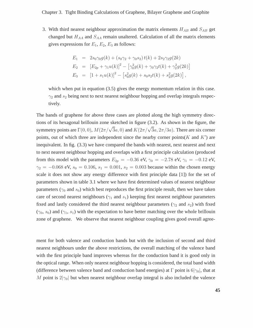
Chapter 3. Tight Binding Calculations of Graphene, BilayerGraphene and Graphite
3. With third nearest neighbour approximation the matrix elementsHAB andSAB get
changed butHAA andSAA remain unaltered. Calculation of all the matrix elements
gives expressions forE1, E2, E3 as follows:
E1 = 2s0γ0g(k) + (s0γ2 + γ0s2) t(k) + 2s2γ2g(2k)
E2 = [E2p + γ1u(k)]2 −[
γ20g(k) + γ0γ2t(k) + γ2
2g(2k)]
E3 = [1 + s1u(k)]2 −[
s20g(k) + s0s2t(k) + s2
2g(2k)]
,
which when put in equation (3.5) gives the energy momentum relation in this case.
γ2 ands2 being next to next nearest neighbour hopping and overlap integrals respec-
tively.
The bands of graphene for above three cases are plotted alongthe high symmetry direc-
tions of its hexagonal brillouin zone sketched in figure (3.2). As shown in the figure, the
symmetry points areΓ(0, 0), M(2π/√
3a, 0) andK(2π/√
3a, 2π/3a). There are six corner
points, out of which three are independent since the nearby corner points(K andK ′) are
inequivalent. In fig. (3.3) we have compared the bands with nearest, next nearest and next
to next nearest neighbour hopping and overlaps with a first principle calculation (produced
from this model with the parametersE2p = −0.36 eV, γ0 = −2.78 eV, γ1 = −0.12 eV,
γ2 = −0.068 eV, s0 = 0.106, s1 = 0.001, s2 = 0.003 because within the chosen energy
scale it does not show any energy difference with first principle data [1]) for the set of
parameters shown in table 3.1 where we have first determined values of nearest neighbour
parameters (γ0 ands0) which best reproduces the first principle result, then we have taken
care of second nearest neighbours (γ1 ands1) keeping first nearest neighbour parameters
fixed and lastly considered the third nearest neighbour parameters (γ2 ands2) with fixed
(γ0, s0) and (γ1, s1) with the expectation to have better matching over the wholebrillouin
zone of graphene. We observe that nearest neighbour coupling gives good overall agree-
ment for both valence and conduction bands but with the inclusion of second and third
nearest neighbours under the above restrictions, the overall matching of the valence band
with the first principle band improves whereas for the conduction band it is good only in
the optical range. When only nearest neighbour hopping is considered, the total band width
(difference between valence band and conduction band energies) atΓ point is6|γ0|, that at
M point is2|γ0| but when nearest neighbour overlap integral is also included the valence
45

Chapter 3. Tight Binding Calculations of Graphene, BilayerGraphene and Graphite
-5
0
5
10
Γ K M ΓWave vcector in A
0 −1
Ene
rgy
in e
V
Figure 3.3: Electronic structure of graphene with first principle result (full curves), firstnearest neighbour interactions (dashed-dotted curves), second nearest neighbour interac-tions (dotted curves) when first nearest neighbour parameters are fixed and third nearestneighbour interactions (dashed curves) when first and second nearest neighbour parame-ters are fixed. The parameters are listed in Table 3.1.
Table 3.1: Tight binding parameters
Neighbours E2p (eV) γ0 (eV) γ1 (eV) γ2 (eV) s0 s1 s2
1st 0.0 -2.74 0.0652nd -0.21 -2.74 -0.07 0.065 0.0023rd -0.21 -2.74 -0.07 -0.015 0.065 0.002 0.001
46
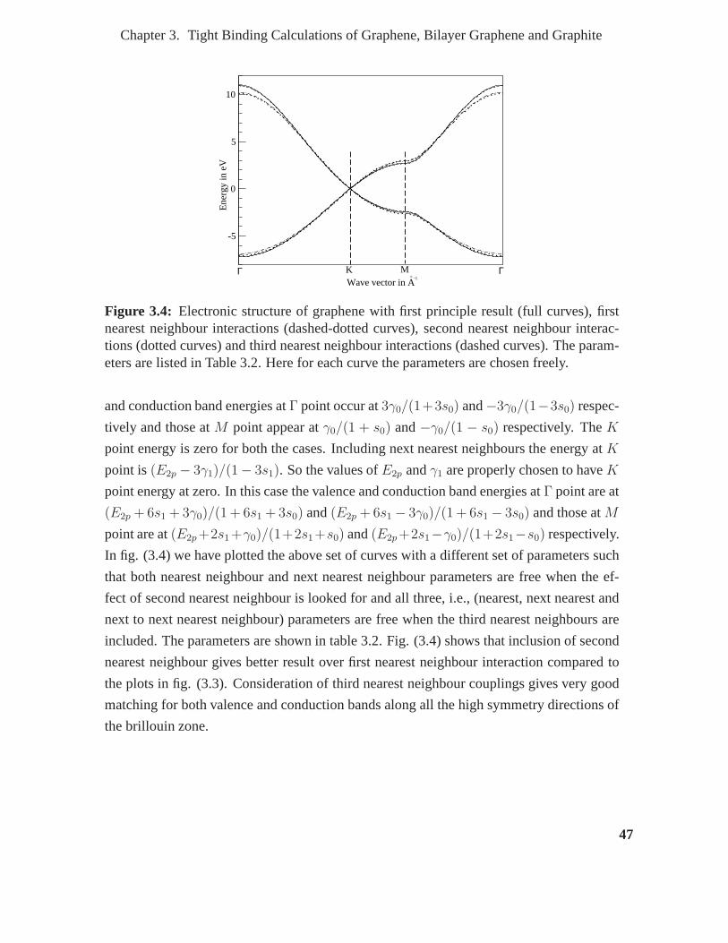
Chapter 3. Tight Binding Calculations of Graphene, BilayerGraphene and Graphite
-5
0
5
10
Γ K M ΓWave vector in A
Ene
rgy
in e
V
0 −1
Figure 3.4: Electronic structure of graphene with first principle result (full curves), firstnearest neighbour interactions (dashed-dotted curves), second nearest neighbour interac-tions (dotted curves) and third nearest neighbour interactions (dashed curves). The param-eters are listed in Table 3.2. Here for each curve the parameters are chosen freely.
and conduction band energies atΓ point occur at3γ0/(1+3s0) and−3γ0/(1−3s0) respec-
tively and those atM point appear atγ0/(1 + s0) and−γ0/(1 − s0) respectively. TheK
point energy is zero for both the cases. Including next nearest neighbours the energy atK
point is(E2p − 3γ1)/(1− 3s1). So the values ofE2p andγ1 are properly chosen to haveK
point energy at zero. In this case the valence and conductionband energies atΓ point are at
(E2p + 6s1 + 3γ0)/(1 + 6s1 + 3s0) and(E2p + 6s1 − 3γ0)/(1 + 6s1 − 3s0) and those atM
point are at(E2p+2s1+γ0)/(1+2s1+s0) and(E2p+2s1−γ0)/(1+2s1−s0) respectively.
In fig. (3.4) we have plotted the above set of curves with a different set of parameters such
that both nearest neighbour and next nearest neighbour parameters are free when the ef-
fect of second nearest neighbour is looked for and all three,i.e., (nearest, next nearest and
next to next nearest neighbour) parameters are free when thethird nearest neighbours are
included. The parameters are shown in table 3.2. Fig. (3.4) shows that inclusion of second
nearest neighbour gives better result over first nearest neighbour interaction compared to
the plots in fig. (3.3). Consideration of third nearest neighbour couplings gives very good
matching for both valence and conduction bands along all thehigh symmetry directions of
the brillouin zone.
47

Chapter 3. Tight Binding Calculations of Graphene, BilayerGraphene and Graphite
Table 3.2: Tight binding parameters
Neighbours E2p (eV) γ0 (eV) γ1 (eV) γ2 (eV) s0 s1 s2
1st 0.0 -2.74 0.0652nd -0.30 -2.77 -0.10 0.095 0.0033rd -0.45 -2.78 -0.15 -0.095 0.117 0.004 0.002
3.3.2 Tight binding band of bilayer graphene
In the following we first present general aspects of the formalism of tight binding band
structure of bilayer graphene and then give details of tightbinding band dispersion under
different situations like: (i) the simplest case with nearest neighbour in-plane and inter-
plane hopping ofπ electrons; (ii) modifications in the bands due to the inclusion of overlap
integrals coming from the same neighbours and due to site energy difference (∆) between
A and B atoms in two different sublattices in the same layer; (iii) effect of in-plane sec-
ond nearest neighbour hopping and corresponding overlap integral; (iv) effect of in-plane
third nearest neighbour hopping and overlap integral on theband near the brillouin zone
corner (K) point and over the whole brillouin zone, and also the density of states of bilayer
graphene corresponding to the above mentioned dispersions. Since bilayer graphene unit
cell contains four atoms coming from two different sublattices of two layers, the Bloch
wave functions for A and B type atoms for each layer [5] are
ΨAik (r) = 1/
√N
∑
Ai
ΦA(r − rAi)eik.rAi and ΨBi
k (r) = 1/√
N∑
Bi
ΦB(r − rBi)eik.rBi ,
wherei refers to layer index,Φ′s arepz atomic orbitals, N is the number of unit cells in the
crystal,CAiandCBi
are contributions to the total wavefunction coming fromith atom of A
and B sublattices respectively. The total wave function is
Ψk(r) =∑
i=1,2
CAiΨAi
k (r) +∑
i=1,2
CBiΨBi
k (r).
48

Chapter 3. Tight Binding Calculations of Graphene, BilayerGraphene and Graphite
With this choice of wavefunction a secular equation including the overlap integrals can be
set up as follows
∣
∣
∣
∣
∣
∣
∣
∣
∣
∣
HA1A1− E(k)SA1A1
HA1B1− E(k)SA1B1
HA1A2− E(k)SA1A2
HA1B2− E(k)SA1B2
HB1A1− E(k)SB1A1
HB1B1− E(k)SB1B1
HB1A2− E(k)SB1A2
HB1B2− E(k)SB1B2
HA2A1− E(k)SA2A1
HA2B1− E(k)SA2B1
HA2A2− E(k)SA2A2
HA2B2− E(k)SA2B2
HB2A1− E(k)SB2A1
HB2B1− E(k)SB2B1
HB2A2− E(k)SB2A2
HB2B2− E(k)SB2B2
∣
∣
∣
∣
∣
∣
∣
∣
∣
∣
= 0,
where H is the Hamiltonian of the system andH′sxiyj
, S′sxiyj
are defined as
Hxiyj=
⟨
Ψxik |H|Ψyj
k
⟩
and Sxiyj=
⟨
Ψxik |Ψyj
k
⟩
respectively.
Herex, y stand for both A and B;i, j can take either of the values 1 and 2. When this
equation is solved for finiteγ0 andγ′
1 only, ignoring the asymmetric energy (∆), in-plane
overlap integral (s0) and the interplane overlap integral (s′
1), the resulting energy eigenval-
ues values are
E1/2(k) = ∓1
2
[
γ′
1 ∓[
γ′21 + 4γ2
0g(k)]1/2
]
and E3/4(k) = ∓1
2
[
γ′
1 ±[
γ′21 + 4γ2
0g(k)]1/2
]
,
where
g(k) =[
1 + 4 cos2 (kya/2) + 4 cos (√
3kxa/2) cos (kya/2)]
,
γ0 = 〈φ(r − rAi|H|φ(r − rBi
〉 ; i being the layer index andγ′
1 = 〈φ(r − rA1|H|φ(r − rA2
〉 .
In a similar wayγ1 andγ2 can be defined. The expansion around theK(
2π/√
3a, 2π/3a)
point gives
E1/4(k) = ±3
4
(
γ20/γ
′
1
)
a2(δk)2,
and E2/3(k) = ±γ′
1 ±3
4
(
γ20/γ
′
1
)
a2(δk)2
whereδk is a small change ink around theK point. From the above results we see that
there are fourπ bands in bilayer graphene. All the bands are parabolic near the brillouin
zone corner. Two of the bands are degenerate with zero energyat theK point. -γ′
1 and
γ′
1 are the energies of the other two bands at that point, i.e.,±γ′
1 is the energy separation
49

Chapter 3. Tight Binding Calculations of Graphene, BilayerGraphene and Graphite
between the highest conduction and the lowest valence bandsat that point. Also the valence
and conduction bands are symmetric over the entire brillouin zone. Since each atomic site
has onepz electron, the Fermi energy (EF ) for undoped bilayer graphene is at zero energy.
The bands are plotted in figure (3.5).
3.3.2.1 Modifications in the bands due to the inclusion of overlap integrals (s0, s′
1)
coming from in-plane and interplane nearest neighbours anddue to breaking
of sublattice symmetry
The secular equation now becomes
∣
∣
∣
∣
∣
∣
∣
∣
∣
∣
E2p + ∆ − E(k) a − bE(k) γ′
1 − s′
1E(k) 0
c − dE(k) E2p − E(k) 0 0
γ′
1 − s′
1E(k) 0 E2p + ∆ − E(k) c − dE(k)
0 0 a − bE(k) E2p − E(k)
∣
∣
∣
∣
∣
∣
∣
∣
∣
∣
= 0, (3.8)
wherea = γ0f(k), b = s0f(k), c = γ0f∗(k), d = s0f
∗(k) and f(k) = eikxa/√
3 +
2e−ikxa/2√
3 cos kya/2, s0 = 〈φ(r − rAi|φ(r − rBi
〉 ands′
1 = 〈φ(r − rA1|φ(r − rA2
〉. In a
similar ways1 ands2 can also be defined. The eigen solutions to the above equationare
E1/2(k) =[
−B1 ±[
B21 − 4A1C1
]1/2]
/2A1 (3.9)
and E3/4(k) =[
−B2 ±[
B22 − 4A2C2
]1/2]
/2A2, (3.10)
where
A1/2 = 1−bd±s′
1, B1/2 = ad+bc∓γ′
1∓s′
1E2p−2E2p−∆, C1/2 = ±γ′
1E2p−ac+E2p(E2p+∆).
Figure (3.5) also shows the bands with finite values of∆, s0 ands′
1 for comparison. We
first discuss the effect of the asymmetry term (∆) on the spectra atK point. The two bands
which are degenerate atK point, are not affected by∆ at that point but the other two bands
appear at energies∆ − γ′
1 and∆ + γ′
1, i.e., though the separation is still±γ′
1, they become
asymmetric with respect to Fermi energy at that point. This term has negligible effect on
the slope of these curves. The lower panel of (a) in fig. (3.5) shows that the lower valence
band comes closer toEF whereas the upper conduction band moves away fromEF when
the sublattice asymmetry is taken care of. Next we illustrate the effect of overlap integrals
50
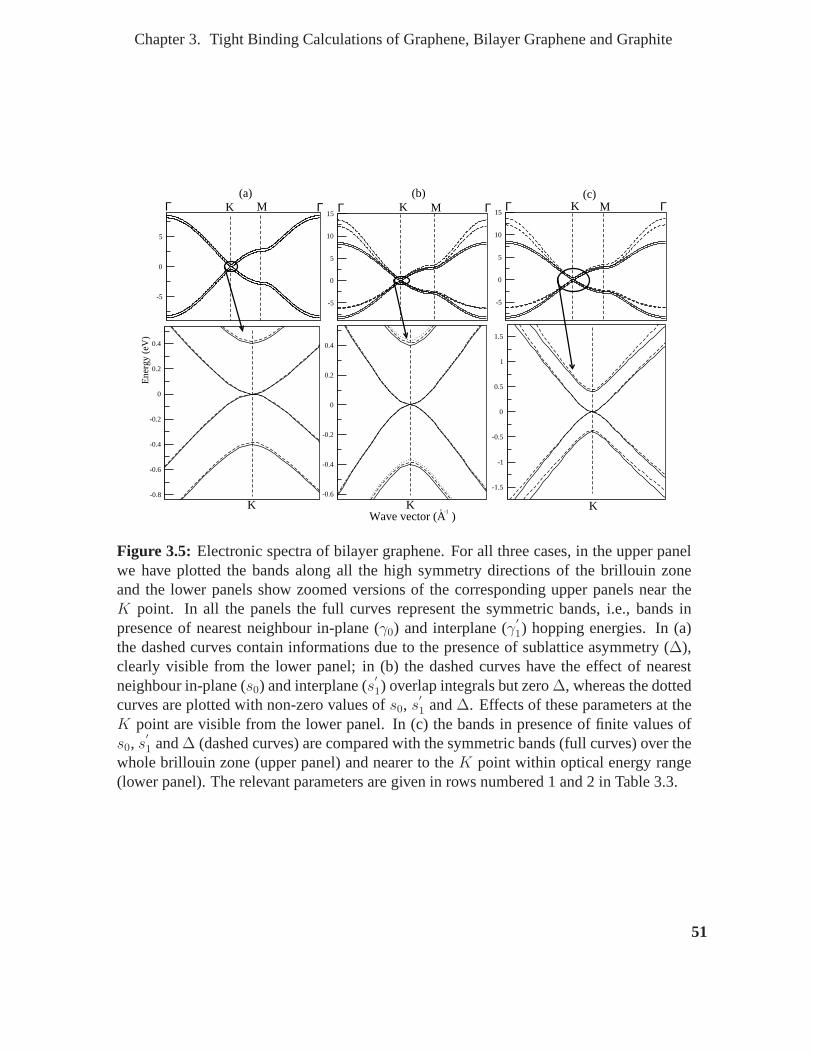
Chapter 3. Tight Binding Calculations of Graphene, BilayerGraphene and Graphite
-5
0
5
-5
0
5
10
15
-5
0
5
10
15
-0.8
-0.6
-0.4
-0.2
0
0.2
0.4
-0.6
-0.4
-0.2
0
0.2
0.4
-1.5
-1
-0.5
0
0.5
1
1.5
(a) (b) (c)Γ K M Γ ΓΓ Γ ΓK KM M
K K K Wave vector (A )
0 -1
Ene
rgy
(eV
)
Figure 3.5: Electronic spectra of bilayer graphene. For all three cases, in the upper panelwe have plotted the bands along all the high symmetry directions of the brillouin zoneand the lower panels show zoomed versions of the corresponding upper panels near theK point. In all the panels the full curves represent the symmetric bands, i.e., bands inpresence of nearest neighbour in-plane (γ0) and interplane (γ
′
1) hopping energies. In (a)the dashed curves contain informations due to the presence of sublattice asymmetry (∆),clearly visible from the lower panel; in (b) the dashed curves have the effect of nearestneighbour in-plane (s0) and interplane (s
′
1) overlap integrals but zero∆, whereas the dottedcurves are plotted with non-zero values ofs0, s
′
1 and∆. Effects of these parameters at theK point are visible from the lower panel. In (c) the bands in presence of finite values ofs0, s
′
1 and∆ (dashed curves) are compared with the symmetric bands (fullcurves) over thewhole brillouin zone (upper panel) and nearer to theK point within optical energy range(lower panel). The relevant parameters are given in rows numbered 1 and 2 in Table 3.3.
51

Chapter 3. Tight Binding Calculations of Graphene, BilayerGraphene and Graphite
s0 ands′
1 atK point. It is observed that the in-plane nearest neighbour overlap integrals0
has no effect atK point because it always appears in product withg(k) which vanishes at
K. But the interlayer overlap integrals′
1, though not altering the degenerate bands, affects
those bands lying further fromEF quite significantly. The upper lying band shifts further
to −γ′
1/(1 − s′
1) and the lower band comes closer toγ′
1/(1 + s′
1) (dashed curves in lower
panel of (b) in fig. (3.5)). The energy separation between them becomes2γ′
1/(1 − s′21 ).
When∆ and overlap integrals are considered together, the upper band shifts even further
to (∆ − γ′
1)/(1 − s′
1) and the lower band comes more close to(∆ + γ′
1)/(1 + s′
1) (dotted
curves in lower panel of (b) in fig. (3.5)). Under this condition the above energy separation
becomes2(γ′
1 − s′
1∆)/(1 − s′21 ). Moreover,s0 ands
′
1 play important role in changing the
slope of the curves. They push off the conduction bands and pull in the valence bands with
respect to Fermi energy almost over the entire energy range,particularly near theΓ point
where the effect is most prominent (dashed curves in upper panel of (c) in fig. (3.5)). With
a closer look over the smaller energy range, i.e., the optical range, we see (in lower panel of
(c)) that the separation between conduction bands increases while that between the valence
bands decreases.
3.3.2.2 Effect of in-plane second nearest neighbour hopping (γ1) and corresponding
overlap integral (s1) on the spectra of bilayer graphene
Since the in-plane next nearest neighbour atoms belong to same sublattice in a plane, we
have in this case
A1/2 = (1 + s1u(k))2 − bd ± s′
1(1 + s1u(k)),
B1/2 = ad + bc ∓ γ′
1(1 + s1u(k)) ∓ s′
1(E2p + γ1u(k))
−(1 + s1u(k))(2E2p + 2γ1u(k) + ∆),
C1/2 = ±γ′
1(E2p + γ1u(k)) − ac + (E2p + γ1u(k))(E2p + γ1u(k) + ∆),
whereu(k) = 2 cos (kya) + 4 cos (kxa√
3) cos (kya/2). The eigen solutions are same as
in equations (3.9) and (3.10) with the modifications inA1, B1, C1 andA2, B2, C2 given
above.
52
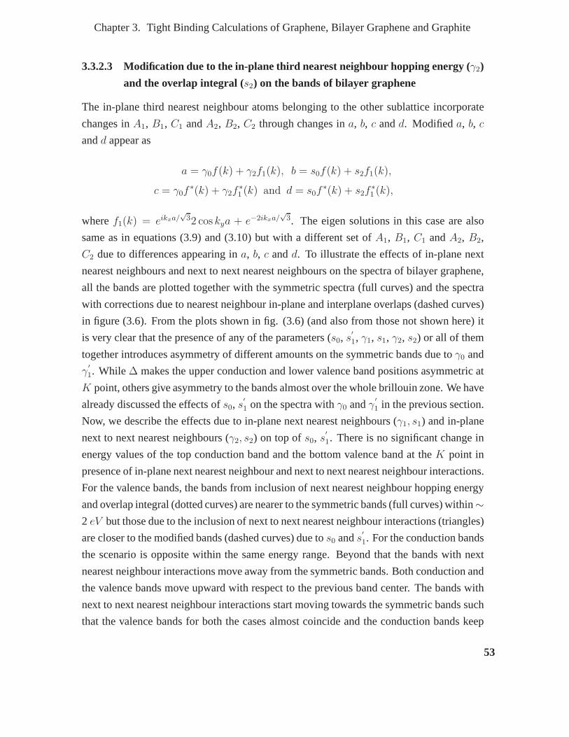
Chapter 3. Tight Binding Calculations of Graphene, BilayerGraphene and Graphite
3.3.2.3 Modification due to the in-plane third nearest neighbour hopping energy (γ2)
and the overlap integral (s2) on the bands of bilayer graphene
The in-plane third nearest neighbour atoms belonging to theother sublattice incorporate
changes inA1, B1, C1 andA2, B2, C2 through changes ina, b, c andd. Modifieda, b, c
andd appear as
a = γ0f(k) + γ2f1(k), b = s0f(k) + s2f1(k),
c = γ0f∗(k) + γ2f
∗1 (k) and d = s0f
∗(k) + s2f∗1 (k),
wheref1(k) = eikxa/√
32 cos kya + e−2ikxa/√
3. The eigen solutions in this case are also
same as in equations (3.9) and (3.10) but with a different setof A1, B1, C1 andA2, B2,
C2 due to differences appearing ina, b, c andd. To illustrate the effects of in-plane next
nearest neighbours and next to next nearest neighbours on the spectra of bilayer graphene,
all the bands are plotted together with the symmetric spectra (full curves) and the spectra
with corrections due to nearest neighbour in-plane and interplane overlaps (dashed curves)
in figure (3.6). From the plots shown in fig. (3.6) (and also from those not shown here) it
is very clear that the presence of any of the parameters (s0, s′
1, γ1, s1, γ2, s2) or all of them
together introduces asymmetry of different amounts on the symmetric bands due toγ0 and
γ′
1. While ∆ makes the upper conduction and lower valence band positionsasymmetric at
K point, others give asymmetry to the bands almost over the whole brillouin zone. We have
already discussed the effects ofs0, s′
1 on the spectra withγ0 andγ′
1 in the previous section.
Now, we describe the effects due to in-plane next nearest neighbours (γ1, s1) and in-plane
next to next nearest neighbours (γ2, s2) on top ofs0, s′
1. There is no significant change in
energy values of the top conduction band and the bottom valence band at theK point in
presence of in-plane next nearest neighbour and next to nextnearest neighbour interactions.
For the valence bands, the bands from inclusion of next nearest neighbour hopping energy
and overlap integral (dotted curves) are nearer to the symmetric bands (full curves) within∼2 eV but those due to the inclusion of next to next nearest neighbour interactions (triangles)
are closer to the modified bands (dashed curves) due tos0 ands′
1. For the conduction bands
the scenario is opposite within the same energy range. Beyond that the bands with next
nearest neighbour interactions move away from the symmetric bands. Both conduction and
the valence bands move upward with respect to the previous band center. The bands with
next to next nearest neighbour interactions start moving towards the symmetric bands such
that the valence bands for both the cases almost coincide andthe conduction bands keep
53

Chapter 3. Tight Binding Calculations of Graphene, BilayerGraphene and Graphite
-5
0
5
10
15
Γ K M Γ
Ene
rgy
(eV
)
Wave vector (A )0 -1
Figure 3.6: Electronic dispersions of bilayer graphene in presence of nearest neighbourin-plane and interplane transfer integrals (full curves),nearest neighbour in-plane andinterplane transfer integrals, overlap integrals and sublattice asymmetric energy (dashedcurves), in-plane next nearest neighbour interactions (dotted curves) and in-plane next tonext nearest neighbour interactions (triangles). The parameters used for these bands aregiven in Table 3.3. The rows numbered 1, 2, 3 and 4 in the table correspond to the curveswith full lines, dashed lines, dotted lines and triangles respectively in the figure.
54

Chapter 3. Tight Binding Calculations of Graphene, BilayerGraphene and Graphite
a separation among themselves aroundΓ point. The values of the parameters used for the
plotted bands are given in Table 3.3, the site energy and transfer integrals are ineV . The
rows numbered 1, 2, 3 and 4 in the table correspond to the curves with full lines, dashed
lines, dotted lines and triangles respectively in figure (3.6) and (3.10).
Table 3.3: Tight binding parameters.γ0, γ1, γ2 andγ′
1 are in eV.
Curves E2p ∆∗ γ0 γ′∗1 γ1 γ2 s0 s
′∗∗1 s1 s2
1 -2.78 -0.42 0.018 -2.78 -0.4 0.117 0.043 -0.45 0.018 -2.78 -0.4 -0.15 0.117 0.04 0.0044 -0.45 0.018 -2.78 -0.4 -0.15 -0.095 0.117 0.04 0.004 0.002
∗taken from reference [18].∗∗chosen as 10 times less than the magnitude ofγ
′
1.
In presence of in-plane next nearest neighbour interactions there are three choices of
E2p (= 3γ1, 3γ1 −∆± γ′
1) for which the Fermi energy comes at zero. For other choices of
E2p the Fermi level shifts from zero. In presence of in-plane next to next nearest neighbour
interactions, the choices ofE2p for which Fermi energy will be at zero, are same as in the
case of next nearest neighbour interactions.
3.3.3 Tight binding band of graphite
Here we shall present a comparative study of the tight binding dispersions of graphite
obtained by following the same prescription used for bilayer graphene. Also, the same set
of tight binding parameters (table 3.3 ) has been utilized. The unit cell of graphite contains
four carbon atoms. The collective wave function of the crystal can be written as
Ψk(r) =∑
i=1,..4
CiΨki , where (3.11)
Ψki (r) =
(
1/√
N)
∑
A/B
ei~k.~rA/Bi ΦA/B(r − r
A/Bi )
Proceeding in the same way as described for bilayer graphene, the dispersion relations in
presence of nearest neighbour in-plane and interplane overlap, i.e., for finiteγ0 and γ′
1
only, ignoring the asymmetric energy (∆), in-plane overlap integral (s0) and the interplane
55

Chapter 3. Tight Binding Calculations of Graphene, BilayerGraphene and Graphite
overlap integral (s′
1), are given as
E1/2(k) = ∓1
2
[
γ′
1fz(k) ∓[
γ′21 f 2
z (k) + 4γ20g(k)
]1/2]
and E3/4(k) = ∓1
2
[
γ′
1fz(k) ±[
γ′21 f 2
z (k) + 4γ20g(k)
]1/2]
,
wherefz(k) = 2 cos (kzc/2), c being unit cell parameter along z-direction.
In presence of nearest neighbour in-plane overlap integral(s0), interplane overlap inte-
gral (s′
1), the asymmetric energy (∆) and in-plane second nearest neighbour hopping (γ1)
and corresponding overlap integral (s1), the energy dispersions change to
E1/2(k) =[
−B1 ±[
B21 − 4A1C1
]1/2]
/2A1 (3.12)
and E3/4(k) =[
−B2 ±[
B22 − 4A2C2
]1/2]
/2A2, (3.13)
where
A1/2 = (1 + s1u(k))2 − bd ± s′
1fz(k)(1 + s1u(k)),
B1/2 = ad + bc ∓ γ′
1fz(k)(1 + s1u(k)) ∓ s′
1fz(k)(E2p + γ1u(k))
−(1 + s1u(k))(2E2p + 2γ1u(k) + ∆),
C1/2 = ±γ′
1fz(k)(E2p + γ1u(k)) − ac + (E2p + γ1u(k))(E2p + γ1u(k) + ∆),
whereu(k), a, b, c andd have been defined in the discussion of bilayer graphene.
The energy eigenvalues in presence of in-plane next to next nearest neighbours are same
as in equations (3.12) and (3.13) with the modifications inA1, B1, C1 andA2, B2, C2 as
has been mentioned in the calculation of bilayer graphene. The above results have been
depicted in figures 3.7 and 3.8. In figure 3.7 (a) the bands withγ0 andγ′
1 only and bands
along with (s0), (s′
1) and (∆) have been compared over the entire brillouin zone. It is found
that in both the cases there are two bondingπ bands and two antibondingπ bands in the
ΓMKΓ plane whereas inAHLA plane theπ bands are degenerate and so are theπ∗ bands.
Widths of the bands at theΓ point increases and slope the bands changes when (s0) and
(s′
1) are included. In fig. 3.7 (b) and (c) the effect of the parameters (s0), (s′
1) and (∆) has
been clearly shown near the zone cornersK andH respectively. From the plots shown and
from the plots which have not been presented here it is noticed that (s0), (s′
1) and (∆) affect
the bands at and near theK point in a manner exactly similar to that of bilayer graphene.
56

Chapter 3. Tight Binding Calculations of Graphene, BilayerGraphene and Graphite
-5
0
5
10
15
-0.5
0
0.5
-0.05
0
0.05
Γ M K A H L AΓ
Ene
rgy
(eV
)
Wave vector (A )0 −1
K H
(a)
(b) (c)
Figure 3.7: Electronic spectra of graphite. The upper panel shows the bands along allthe high symmetry directions of the graphite brillouin zoneand in the lower panels wehave shown the zoomed versions of the spectra near the brillouin zone corners (K andH points). In all the panels the full curves represent the symmetric bands, i.e., bandsin presence of nearest neighbour in-plane (γ0) and interplane (γ
′
1) hopping energies. In(a) the dashed curves contain informations due to the presence of sublattice asymmetry(∆), nearest neighbour in-plane (s0) and interplane (s
′
1) overlap integrals. Effects of theseparameters at and around theK andH points are visible from the lower panel (in (b)and(c) respectively). The relevant parameters are given in rows numbered 1 and 2 in Table 3.3.
57
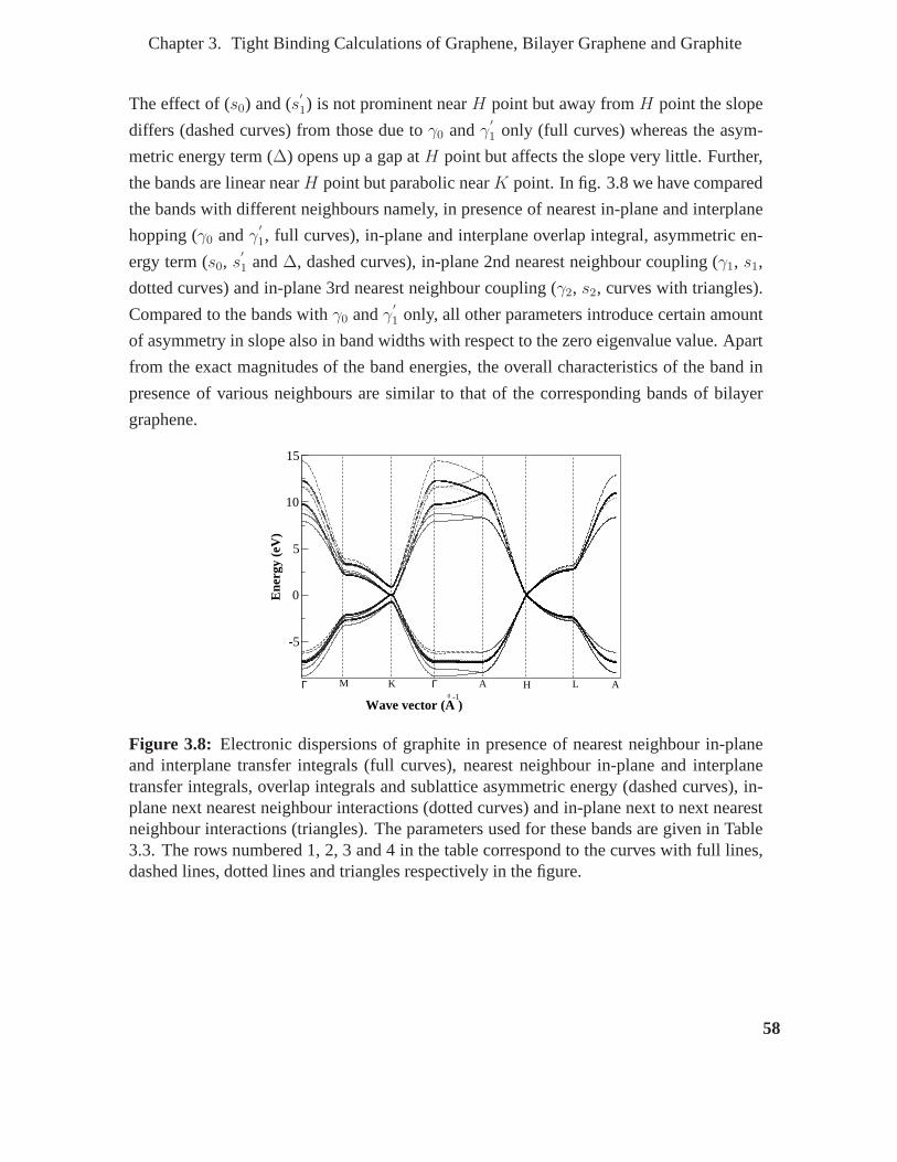
Chapter 3. Tight Binding Calculations of Graphene, BilayerGraphene and Graphite
The effect of (s0) and (s′
1) is not prominent nearH point but away fromH point the slope
differs (dashed curves) from those due toγ0 andγ′
1 only (full curves) whereas the asym-
metric energy term (∆) opens up a gap atH point but affects the slope very little. Further,
the bands are linear nearH point but parabolic nearK point. In fig. 3.8 we have compared
the bands with different neighbours namely, in presence of nearest in-plane and interplane
hopping (γ0 andγ′
1, full curves), in-plane and interplane overlap integral, asymmetric en-
ergy term (s0, s′
1 and∆, dashed curves), in-plane 2nd nearest neighbour coupling (γ1, s1,
dotted curves) and in-plane 3rd nearest neighbour coupling(γ2, s2, curves with triangles).
Compared to the bands withγ0 andγ′
1 only, all other parameters introduce certain amount
of asymmetry in slope also in band widths with respect to the zero eigenvalue value. Apart
from the exact magnitudes of the band energies, the overall characteristics of the band in
presence of various neighbours are similar to that of the corresponding bands of bilayer
graphene.
-5
0
5
10
15
Ene
rgy
(eV
)
Γ M K A H L AΓ
Wave vector (A )0 -1
Figure 3.8: Electronic dispersions of graphite in presence of nearest neighbour in-planeand interplane transfer integrals (full curves), nearest neighbour in-plane and interplanetransfer integrals, overlap integrals and sublattice asymmetric energy (dashed curves), in-plane next nearest neighbour interactions (dotted curves)and in-plane next to next nearestneighbour interactions (triangles). The parameters used for these bands are given in Table3.3. The rows numbered 1, 2, 3 and 4 in the table correspond to the curves with full lines,dashed lines, dotted lines and triangles respectively in the figure.
58

Chapter 3. Tight Binding Calculations of Graphene, BilayerGraphene and Graphite
3.4 Density of states
In fig. 3.9 (a) we have plotted the density of states (due toπ band) of graphene for near-
est neighbour interaction only without (full curve) and with (dashed-dotted curve) overlap
integral correction. It shows that without overlap integral valence and conduction bands
-5 0 5 10
Den
sity
of s
tate
s (a
rb. u
nit)
-5 0 5 10 -5 0 5 10
Energy (eV)
(a) (b) (c)
Figure 3.9: Density of states of graphene (a) with nearest neighbour hopping but zero over-lap integral (full curve) and with nearest neighbour hopping and overlap integral (dashed-dotted curve), (b) derived from the bands in fig. 3.3 (parameters are in Table 3.1). Firstprinciple result (full curve), first nearest neighbour interactions (dashed-dotted curve), sec-ond nearest neighbour interactions (dotted curve) and third nearest neighbour interactions(dashed curve) and (c) calculated from the bands plotted in fig. 3.4 (parameters are in Table3.2). First principle result (full curve), first nearest neighbour interactions (dashed-dottedcurve), second nearest neighbour interactions (dotted curve) and third nearest neighbourinteractions (dashed curve).
are symmetric but in presence of overlap integral width of valence band decreases and that
of conduction band increases. Since there are two atoms in each unit cell and each carbon
atom has one electron inpz state, the valence band is completely filled and hence, the Fermi
level lies at the top of the valence band at zero energy which appears atK andK ′ points of
the brillouin zone in energy momentum space. Graphene has zero density of states at Fermi
energy and over a very small energy range around zero (i.e.,K point energy around which
energy dispersion is also linear in momentum) the density ofstates is varying linearly with
energy. Due to the flat part of the band nearM point of brillouin zone Van Hove singu-
larities are arising in density of states. The positions of the singular points are symmetric
in absence of overlap term while the singularity moves slightly towards Fermi energy for
valence band and goes slightly away from Fermi energy for conduction bands with overlap
59

Chapter 3. Tight Binding Calculations of Graphene, BilayerGraphene and Graphite
-5 0 5 10 15
Den
sity
of s
tate
s (a
rb. u
nit)
Energy (eV)
Figure 3.10: Density of states of bilayer graphene in presence of nearestneighbour in-plane and interplane transfer integrals (full curves), nearest neighbour in-plane and in-terplane transfer integrals, overlap integrals and sublattice asymmetric energy (dashedcurves), in-plane next nearest neighbour interactions (dotted curves) and in-plane next tonext nearest neighbours (triangles). The parameters used in these curves are given in Table3.3.
(s0). In figure 3.9 (b) and (c) the density of states have been plotted as per the bands in fig.
(3.3) and (3.4). Here we see that though the density of statesis linear near Fermi energy,
it becomes asymmetric due to the presence of second and thirdnearest neighbour interac-
tions. As expected the density of states in presence of thirdnearest neighbours is matching
well with the density of states due to first principle bands when the parameters are chosen
freely. In all other cases the band width is changing slightly and positions of Van Hove
singularities are changing over a narrow energy range. Whencompared with ref. [9], the
density of states in presence of second nearest neighbours shows a noticeable difference.
It is observed that when the second nearest neighbours are chosen for good fitting of low
energy part of the spectrum, it gives rise to another Van Hovesingularity at conduction
band edge but that is removed if the parameters are such that it gives good agreement over
the whole energy range. Also, that is suppressed in presenceof third nearest neighbour
interactions.
The density of states (DOS) of bilayer graphene corresponding to the bands in fig. (3.6)
with the parameters in Table 3.3 are shown in figure (3.10). From these curves it is ev-
ident that the finite, though small, density of states (DOS) at the zero energy of bilayer
graphene remains unaffected due to the presence of factors which lead to asymmetry in
bands. Further, the slope of the density of states curves within < 0.5 eV does not change
due to the factors mentioned above. Rather, they have prominent effect in bringing asym-
metry in band widths. To illustrate, we see that when only nearest neighbour in-plane and
60

Chapter 3. Tight Binding Calculations of Graphene, BilayerGraphene and Graphite
-5 0 5 10 15Energy (eV)
Den
sity
of S
tate
s (a
rb. u
nit)
Figure 3.11: Density of states of graphite in presence of nearest neighbour in-plane andinterplane transfer integrals (full curves), nearest neighbour in-plane and interplane transferintegrals, overlap integrals and sublattice asymmetric energy (dashed curves), in-plane nextnearest neighbour interactions (dotted curves) and in-plane next to next nearest neighbours(triangles). The parameters used in these curves are given in Table 3.3.
interplane transfer energies (γ0 andγ′
1) are there, valence band DOS and conduction band
DOS (full curves) are exactly symmetric with respect to the Fermi energy at zero, that is
the band widths are same. Also the van Hove singularities areat symmetric positions, the
scenario being consistent with the corresponding band structure. As soon as the nearest
neighbour in-plane and interplane overlap integrals (s0 ands′
1) are taken into account the
valence band (VB) DOS and conduction band (CB) DOS (dashed curves) start becoming
asymmetric, i.e., the band widths become different: valence band becomes narrow and
conduction band widens. Moreover, the van Hove singularities in VB come closer toEF
whereas those in CB move away fromEF . In presence of in-plane second nearest neigh-
bours (dotted curves) CB becomes slightly narrow and VB slightly wide compared to the
previous case, though VB is still narrower compared to CB. There is no significant change
in the positions of the van Hove singularities in this case when compared with the previous
one. In-plane third nearest neighbour interactions do not have much effect on the widths of
the bands on top of that of the in-plane second nearest neighbour interactions but bring the
van Hove singularities slightly nearer to the Fermi energy.It is also observed that the sub-
lattice asymmetric energy (∆) does not have any significant effect on the density of states
of bilayer graphene.
In figure 3.11 the density of states of graphite corresponding to the bands in fig. (3.8)
with the parameters in Table 3.3 are shown. Though little buta finite density of states
are present at zero energy. Apart from the nature of the van Hove singularities, the overall
appearance of the density of states obtained from the bands due to different coupling param-
61
Chapter 3. Tight Binding Calculations of Graphene, BilayerGraphene and Graphite
eters is similar to those of bilayer graphene (fig. 3.11). There is one van Hove singularity
in each band of monolayer graphene and bilayer graphene had two adjacent singularities
in each band. In three dimensional graphite it appears as a rise in the density of states
rather than the spike like features in monolayer and bilayergraphene, i.e., the singularities
become smoother. It needs to be mentioned that all the density of states data presented here
are not absolute values, they are arbitrary up to a normalization factor.
3.5 Summary and Conclusion
To summarize, we have calculated the electronic spectrum and density of states of graphene
including up to third nearest neighbour interactions and got a set of tight binding parame-
ters on the physical ground that the absolute values of the parameters should decrease as
one moves from first nearest neighbour towards higher distance. This set of parameters has
been used to see the effect of in-plane first nearest neighbour overlap integral (s0), second
(γ1, s1) and third (γ2, s2) nearest neighbour interactions on the band structure of bilayer
graphene also. We have illustrated the role of these parameters in governing electron-hole
asymmetry in the band structure of bilayer graphene within tight binding model. When
compared the role of site energy difference (∆) between A and B sublattices in the same
graphene layer on the electronic spectra of single layer graphene and bilayer graphene, a
distinct difference is observed between the two systems. Sublattice asymmetry in mono-
layer graphene introduces a gap in the spectra at theK point whereas in bilayer it does
not induce gap in the spectra, rather it gives an asymmetry inthe energy values of the top
valence and bottom conduction bands with respect to the energy at which the other two
bands are degenerate. Moreover, in presence of∆ the gap between top valence and bottom
conduction bands at theK point remains intact to±γ′
1 which is the separation even without
∆. Apart from∆ the other important factor which contributes significantlyto the values of
the top valence and bottom conduction bands atK point is the interlayer nearest neighbour
overlap integral (s′
1). Hence, we find thatEc (top) andEv (bottom) are functions of∆ and
s′
1 both atK point. Regarding this, Z. Q. Li et al. [18] discuss only the dependence on∆.
Our study suggests for the consideration of a model containing both∆ ands′
1 for a more
accurate determination of∆ from experimental results. Further, we observe a considerable
change in the slope of the bands in presence of nearest neighbour in-plane and interplane
overlap integrals (s0 ands′
1) compared to those with nearest neighbour in-plane and inter-
layer coupling energies (γ0 andγ′
1) only. Z. Q. Li et al. [18] have discussed the induction of
62
Chapter 3. Tight Binding Calculations of Graphene, BilayerGraphene and Graphite
electron-hole asymmetry in the slope of valence and conduction bands due to next nearest
neighbour interlayer coupling energy (γ4) but without overlap integrals. It is noted there
that with a finite value ofγ4, two conduction bands are closer and the valence bands are
further apart atk values away from theK point. We observe that finite values ofs0 ands′
1
also give electron-hole asymmetry in the slope of valence and conduction bands but with
an opposite trend compared to the bands withγ4. With finite values ofs0 ands′
1 the con-
duction bands move further from each other and the valence bands come closer fork values
away from theK point. It could be concluded from this comparative study that the com-
bined effect ofγ4, s0 ands′
1 could make some balance between the above two cases, may
not be a complete balance to get back the symmetric spectra with only γ0 andγ′
1 but the
degree of electron-hole asymmetry in slope of the bands willget modified nevertheless. A
model includingγ4, s0 ands′
1, though very complicated to handle, may lead to more accu-
rate determination of the important parameter likeγ′
1 when comparing experimental results
having asymmetry in electron and hole sides. With in-plane next nearest neighbour interac-
tions (γ1 ands1) the trend of electron-hole asymmetry in slope of bands remains similar as
that withs0 ands′
1 but the asymmetry in valence and conduction band widths nearΓ point
is reduced compared to that with zero values ofγ1 ands1. Moreover, in this case if the site
energy termE2p is not chosen properly there will be a shift in Fermi energy [19]. In-plane
third nearest neighbour interactions (γ2 ands2) do not affect much on top of in-plane sec-
ond nearest neighbour interactions except very little change in band widths atΓ point and
slight modifications in the slope of the bands. Hence, as far as electron-hole asymmetry
in slope of valence and conduction bands is concerned, a Hamiltonian includings0, s′
1 and
in-plane second nearest neighbour interactions (γ1 ands1) could be sufficient to interpret
experimental results (e.g. the cyclotron resonance data) with asymmetry in electron and
hole sides. Also, the in-plane third nearest neighbour interactions could be more useful
in determining all the above mentioned parameters by fittingbilayer graphene bands with
first principle results or with angle resolved photoemission data over the whole brillouin
zone. Within similar formalism, we have also shown the effects of in-plane nearest, next
nearest and next to next nearest neighbour couplings along with the nearest interlayer cou-
pling on the band structure of three dimensional graphite. NearK point the effect of these
parameters mimics those of bilayer graphene whereas atH point a gap is opened up by the
asymmetric energy∆ but s0 ands′
1 incorporate only changes in slope of the bands.
63

Chapter 3. Tight Binding Calculations of Graphene, BilayerGraphene and Graphite
3.6 Derivation of the electronic dispersions of graphene in
presence of different neighbours
In this last section, as mentioned earlier, we present some details of the derivations of
the dispersion relations of graphene in presence of variousnearest neighbours. The cor-
responding matrix elements in equation (3.4) are computed here in presence of different
neighbours.
1. For nearest neighbour approximation, we have
HAA = (1/N)∑
A
ei~k.(~rA−~rA) 〈ΦA(r − rA)|H|ΦA(r − rA)〉 ≈ E2p,
SAA = 〈ΦA(r − rA)|ΦA(r − rA)〉 = 1,
because the wave functions are normalized;
HAB = γ0
∑
B
ei~k.(~rB−~rA) = γ0f(k), SAB = s0f(k) where
γ0 = (1/N)∑
A
〈ΦA(r − rA)|H|ΦB1(r − rB1
)〉 ,
s0 = (1/N)∑
A
〈ΦA(r − rA)ΦB1(r − rB1
)〉 , and
f(k) = eikxa/√
3 + 2e−ikxa/2√
3 cos kya/2.
Hence
E0 = E2p, E1 = 2γ0s0|f(k)|2, E2 = E22p − γ2
0 |f(k)|2 and,
E3 = 1 − s20|f(k)|2 with
|f(k)|2 = g(k) = 1 + 4 cos2 (kya/2) + 4 cos (√
3kxa/2) cos (kya/2),
leading to
E±(k) =
[
(E2p − s0γ0g(k)) ± (γ0 − s0E2p)√
g(k)]
[1 − s20g(k)]
. (3.14)
64

Chapter 3. Tight Binding Calculations of Graphene, BilayerGraphene and Graphite
From the secular determinant the dispersion can alternatively be written as [8]
E±(k) =(
E2p ± γ0
√
g(k))
/(
1 ± s0
√
g(k))
. (3.15)
2. For second nearest neighbour approximation we need the matrix elementsHAA and
SAA only as these two are affected by next nearest neighbours. These are
HAA =
∫
Ψ∗kA (r)HΨk
A(r)d~r = E2p + γ1u(k),
SAA = 1 + s1u(k), where
u(k) = 2 cos (kya) + 4 cos (kxa√
3) cos (kya/2),
γ1 = (1/N)∑
A2
〈ΦA2(r − rA2
)|H|ΦA(r − rA)〉 , and
s1 = (1/N)∑
A2
〈ΦA2(r − rA2
)|ΦA(r − rA)〉 .
Putting all the above elements in the secular determinant weget
E±(k) =[
E2p + γ1u(k) ∓ γ0
√
g(k)]
/[
1 + s1u(k) ∓ s0
√
g(k)]
. (3.16)
3. In presence of third nearest neighbours only the matrix elementsHAB andSAB get
changed butHAA andSAA remain unchanged. Hence
HAB =
∫
Ψ∗kB (r)HΨk
A(r)d~r = γ0f(k) + γ2v(k),
SAB = s0f(k) + s2v(k), where
γ2 = (1/N)∑
A
〈ΦA(r − rA)|H|ΦB3(r − rB3
)〉 ,
s2 = (1/N)∑
A
〈ΦA(r − rA)|ΦB3(r − rB3
)〉 and
v(k) = eikxa/√
32 cos kya + e−2ikxa/√
3.
65

Chapter 3. Tight Binding Calculations of Graphene, BilayerGraphene and Graphite
Therefore, expressions forE1, E2, E3 are
E1 = 2s0γ0g(k) + (s0γ2 + γ0s2) t(k) + 2s2γ2g(2k)
E2 = [E2p + γ1u(k)]2 −[
γ20g(k) + γ0γ2t(k) + γ2
2g(2k)]
E3 = [1 + s1u(k)]2 −[
s20g(k) + s0s2t(k) + s2
2g(2k)]
, where
g(2k) = 1 + 4 cos2 (kya) + cos (√
3kxa) cos (kya) and
t(k) = 2 cos (kxa√
3) + 4 cos (kya) + 4 cos (kya/2) cos (kxa√
3/2)
+8 cos (kya) cos (kya/2) cos (kxa√
3/2).
66

Bibliography
[1] S. Reich, J. Maultzsch, C. Thomsen and P. Ordejón,Phys. Rev.B66, 035412 (2002).
[2] B. T. Kelly, Physics of Graphite(Applied Science Publishers, London and New Jer-
sey, 1981).
[3] P. R. Wallace,Phys. Rev.71, 622 (1947).
[4] Novoselov, K. S., A. K. Geim, S. V. Morozov, D. Jiang, Y. Zhang, S.V. Dubonos, I.V.
Gregorieva and A. A. Firsov,Science306, 666 (2004).
[5] B. Partoens and F. M. Peeters,Phys. Rev.B74, 075404 (2006).
[6] A. Bostwick, T. Ohta, T. Seyller, K. Horn and E. Rotenberg, Nature Physics3, 36-40
(2007).
[7] R. Roldán, M. P. López-Sancho and F. Guinea “Effect of electron-electron interaction
on the Fermi surface topology of doped graphene”, arXiv:0710.3034v1 [cond-mat.str-
el] (2007).
[8] R. Saito, G. Dresselhaus and M.S. Dresselhaus:Physical Properties of Carbon Nan-
otubes(chap.2 and 4) (Imperial College Press, London, 1998).
[9] A. H. Castro Neto, F. Guinea, N. M. R. Peres, K. S. Novoselov and A. K. Geim,Rev.
Mod. Phys.81, 109 (2009).
[10] Edward McCann,Phys. Rev.B74, 161403(R) (2006).
[11] Hongki Min, B.R. Sahu, Sanjay K. Banerjee, A.H. MacDonald, Phys. Rev.B75,
155115 (2007).
[12] E. V. Castro, K. S. Novoselov, S. V. Morozov, N. M. R. Peres, J. M. B. Lopes dos
Santos, J Nilsson, F. Guinea, A. K. Geim, and A. H. Castro Neto, Phys. Rev. Lett.99,
216802 (2007).
[13] J. B. Oostinga, H.B. Heersche, X Liu, A.F. Morpurgo and L. M.K. Vandersypen,
Nature Materials7 151-157 (2007).
[14] Y. Zhang, Tsung-Ta Tang, C. Girit, Z. Hao, Michael C. Martin, A. Zettl, Michael F.
Crommie, Y. Ron Shen and F. Wang,Nature459, 820-823 (2009).
67

Bibliography
[15] T. Ohta, A. Bostwick, T. Seyller, K. Horn, and E. Rotenberg,Science313, 951 (2006).
[16] L.M. Malard, J. Nilsson, D.C. Elias, J.C. Brant, F. Plentz, E.S.Alves, A.H. Castro
Neto and M. A. Pimenta,Phys. Rev.B76, 201401(R) (2007).
[17] A. Grüneis, C. Attaccalite, L. Wirtz, H. Shiozawa R. Saito, T. Pichler, A. Rubio,
“Tight-binding description of the quasiparticle dispersion of graphite and few-layer
graphene”, arXiv:0808.1467v2 [cond-mat.mtrl-sci] (2008).
[18] Z. Q. Li, E. A. Henriksen, Z. Jiang, Z. Hao, M. C. Martin, P. Kim, H. L. Stormer, and
D. N. Basov,Phys. Rev. Lett.102, 037403 (2009).
[19] A. R. Wright, Feng Liu, and C. Zhang, “Effect of next-nearest neighbor coupling
on the optical spectra in bilayer graphene”, arXiv:0907.0504v1 [cond-mat.mtrl-sci]
(2009).
[20] J. W. McClure,Phys. Rev.108, 612 (1957).
68

4Band Structure of single crystal graphite
and HOPG from ARPES and KRIPES
4.1 Introduction
The recent discovery of zero dimensional fullerene, one dimensional carbon nanotubes and
the research activities on the very recently found two dimensional material graphene have
given an impetus to the reinvestigation of some of the exoticand fundamentally important
physical properties of carbon based materials. Like graphene, which shows a peculiar low
energy electronic spectrum due to its sublattice structure, graphite also has a linear dis-
persion near theH point along with its quadratic band near theK point of its Brillouin
zone [1]. Many physical properties like the transport and magnetic behaviours, in single
crystal graphite and in highly oriented pyrolytic graphite(HOPG) [2–5] are not well un-
derstood and might be governed by the carrier dynamics near their Fermi energy (EF ). The
near EF electronic structure on both the occupied and unoccupied sides are important for a
consolidated understanding of the physics behind these properties. There have been many
experimental studies [6–10] earlier on the electronic structure of the occupied states of
graphite in which various bands were unambiguously identified using monochromatic light
sources or synchrotron radiation. There are lot of PES studies (angle integrated and angle
resolved) on HOPG and single crystal graphite along with many intercalated compounds
of graphite. Although, the electronic structure studies ongraphite seems to be complete,
recent works have shown several new results owing mainly to the improved experimen-
tal techniques. On the other hand, along with ARPES study on graphite to determine its
occupied band structure, a significant amount of effort was also put to study the unoccu-
69
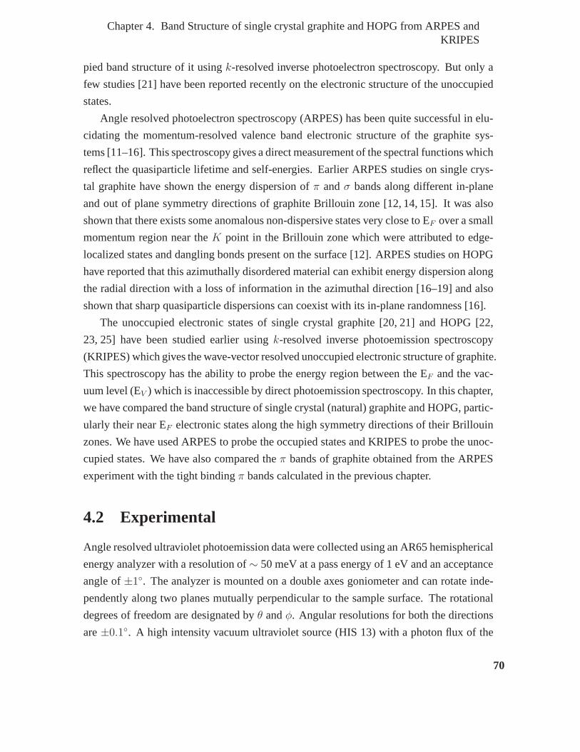
Chapter 4. Band Structure of single crystal graphite and HOPG from ARPES andKRIPES
pied band structure of it usingk-resolved inverse photoelectron spectroscopy. But only a
few studies [21] have been reported recently on the electronic structure of the unoccupied
states.
Angle resolved photoelectron spectroscopy (ARPES) has been quite successful in elu-
cidating the momentum-resolved valence band electronic structure of the graphite sys-
tems [11–16]. This spectroscopy gives a direct measurementof the spectral functions which
reflect the quasiparticle lifetime and self-energies. Earlier ARPES studies on single crys-
tal graphite have shown the energy dispersion ofπ andσ bands along different in-plane
and out of plane symmetry directions of graphite Brillouin zone [12, 14, 15]. It was also
shown that there exists some anomalous non-dispersive states very close to EF over a small
momentum region near theK point in the Brillouin zone which were attributed to edge-
localized states and dangling bonds present on the surface [12]. ARPES studies on HOPG
have reported that this azimuthally disordered material can exhibit energy dispersion along
the radial direction with a loss of information in the azimuthal direction [16–19] and also
shown that sharp quasiparticle dispersions can coexist with its in-plane randomness [16].
The unoccupied electronic states of single crystal graphite [20, 21] and HOPG [22,
23, 25] have been studied earlier usingk-resolved inverse photoemission spectroscopy
(KRIPES) which gives the wave-vector resolved unoccupied electronic structure of graphite.
This spectroscopy has the ability to probe the energy regionbetween the EF and the vac-
uum level (EV ) which is inaccessible by direct photoemission spectroscopy. In this chapter,
we have compared the band structure of single crystal (natural) graphite and HOPG, partic-
ularly their near EF electronic states along the high symmetry directions of their Brillouin
zones. We have used ARPES to probe the occupied states and KRIPES to probe the unoc-
cupied states. We have also compared theπ bands of graphite obtained from the ARPES
experiment with the tight bindingπ bands calculated in the previous chapter.
4.2 Experimental
Angle resolved ultraviolet photoemission data were collected using an AR65 hemispherical
energy analyzer with a resolution of∼ 50 meV at a pass energy of 1 eV and an acceptance
angle of±1◦. The analyzer is mounted on a double axes goniometer and can rotate inde-
pendently along two planes mutually perpendicular to the sample surface. The rotational
degrees of freedom are designated byθ andφ. Angular resolutions for both the directions
are±0.1◦. A high intensity vacuum ultraviolet source (HIS 13) with a photon flux of the
70

Chapter 4. Band Structure of single crystal graphite and HOPG from ARPES andKRIPES
order of1016 photons/s/sr at the HeI (21.2 eV) line and a beam spot size of 2.5 mm di-
ameter was used. The samples studied were natural graphite commercially obtained from
NGS Naturgraphit GmbH and highly oriented pyrolitic graphite of grade SPI-1 commer-
cially supplied by SPI Supplies Division of Structure Probe, Inc. The angular spread of the
c-axes of the crystallites for the above mentioned grade of HOPG is∼ 0.4◦ ± 0.1◦. Both
natural single crystal graphite and HOPG samples were cleaved insitu using post technique
under a base vacuum of∼ 2.5 × 10⁻¹⁰ mbar in the preparation chamber and were imme-
diately transferred to the analysis chamber. The orientations of the crystal surfaces were
determined by low energy electron diffraction (LEED) performed in the analysis chamber
at a base pressure of∼ 2.8 × 10⁻¹¹ mbar. Before doing photoemission experiment the
samples were freshly cleaved again to avoid any unwanted surface contamination due to
LEED experiment on the samples. The Fermi energy was calibrated using the Fermi edge
spectra of silver, freshly evaporated on to a sample holder.
The inverse photoemission experiments were carried out with an KRIPES spectrometer
in the isochromat mode with a mean photon energy of 9.9 eV. Thespectrometer consists of
a low-energy Stoffel-Johnson type electron gun and a band-pass Geiger-Müller type photon
detector with acetone gas filling and CaF2 window (acetone/CaF2) [26]. The overall energy
resolution of the spectrometer is 0.55 eV. The spectra have been normalized by dividing the
photon counts from the acetone/CaF2 detector by the incident electron beam current, as in
our other works [27]. The system is also equipped with a low energy electron diffraction
(LEED) unit which was used to determine the orientation of single crystal graphite and to
check the surface cleanliness of HOPG sample by looking at the sharpness of its diffrac-
tion ring. Both the samples were cleaved insitu with an adhesive tape at a pressure of∼1.6 × 10⁻⁸ mbar in the preparation chamber. The experiments were performed at a base
pressure of∼ 6 × 10⁻¹⁰ mbar in the main chamber. Momentum-resolved spectra were
collected by rotating the sample (say byθ◦) with respect to the incident electron beam at
an angular interval of5◦. The Fermi energy was calibrated by using the spectrum takenon
a polycrystalline silver sample.
4.3 Results and Discussions
Figure 4.1(a) shows the ARPES spectra of the single crystal graphite sample taken at room
temperature along theΓK direction of its Brillouin zone (marked by the thick arrow in
inset) by using He I excitation line. The high symmetry directions of the sample were
71

Chapter 4. Band Structure of single crystal graphite and HOPG from ARPES andKRIPES
determined from its low energy electron diffraction (LEED)pattern (fig. 4.2) having six
bright spots which indicates the hexagonal symmetry of the surface. It can be seen from the
figure that the spectrum at theΓ point has three weak features at∼ 2.8 eV,∼ 8.3 eV and∼10.3 eV. The peak at around 8.3 eV could be from the bottom of the lowerπ band. Along
theΓK direction we find two dispersing bands; one moving towards higher binding energy
up to∼ 9.8 eV and the other dispersing strongly towards Fermi energy. Earlier reported
ARPES measurements [11,12] and band structure calculations [28–31] have identified this
strongly dispersing band as the valenceπ band. Near about theK point of the Brillouin
zone, this band splits into the upperπ band (π1) and the lowerπ band (π2). In order to
estimate the splitting between the twoπ bands at theK point, spectrum was taken over a
smaller energy range at that point (spectrum marked as K in figure 4.1(c)). To visualize
the dispersion of the nearK-point features more clearly, a few spectra at and around theK
point along the cut marked as A (in the inset) over an energy range of∼ 3.5 eV are shown in
fig. 4.1(c). The splitting between the twoπ bands at theK point is∼ 0.5 eV, comparable
to the value reported earlier [11, 13–15] in the literature.This splitting arises due to the
coupling between adjacent layers in graphite. In figure 4.1(d) theK-point spectra over a
very small energy range (∼ 0.6 eV) taken at room temperature and at 77 K are compared.
It is observed that the spectral feature sharpens at lower temperature. This spectral feature
could be ascribed to the formation of quasiparticles due to the coupling ofπ electrons
with the collective excitations such as phonon. The sharpening of this feature shows the
increased lifetime of these quasiparticles at low temperature. Presence of the quasiparticles
demonstrate the strong electron-phonon coupling in graphite. A recent study by Sugawara
et al [13] on kish graphite has reported about a sharp peak appearing at low temperature
very close to theK point within 200 meV below EF and it becomes extremely sharp at
theK point. This strong enhancement of spectral intensity is explained by the formation
of quasiparticles due to coupling ofπ electrons with some collective excitation, namely
phonon. Ref. [13] has also found the existence of another sharp peak above EF originating
from antibondingπ∗ band and the estimated separation between the peaks due toπ andπ∗
bands at theK point at 260 K temperature is 25 meV. In our spectrum at theK point taken
at room temperature the quasiparticle peak due toπ∗ band is not visible, could be due to
poor instrumental resolution. They have shown that the linear energy dependence of this
quasiparticle scattering rate indicates a non Fermi-liquid behaviour of electrons in graphite.
In figure 4.1(b), the dispersion of theπ band towards EF is presented graphically by plotting
the photoemission intensity against the energy and momentum component parallel to the
72

Chapter 4. Band Structure of single crystal graphite and HOPG from ARPES andKRIPES
surface.
The ARPES spectra taken alongΓM direction of the Brillouin zone of the single crystal
graphite sample is shown in figure 4.3(a). The spectra show anintense peak moving up to
∼ 2.8 eV below the Fermi energy. Apart from this, there is one feature at∼ 10.3 eV which
does not disperse with changes in emission angles whereas another feature at∼ 7.8 eV
appearing at higher emission angles disperses towards lower binding energy as the emission
angles decrease. It can be seen from Fig. 4.3(a) that at some point the broad hump, present
in theΓ point spectrum, splits into two bands: one goes towards higher binding energy up
to ∼ 7.8 eV and the other disperses up to∼ 2.8 eV below Fermi energy near theM point
of Brillouin zone. Dispersion of this band is clearly visible in the intensity plot shown in
figure 4.3(b). It is also observed that the feature at∼ 2.8 eV becomes very intense and
remains non-dispersive over a certain angular range near the M point, consistent with the
reported dispersion near this point.
In order to compare our results in different high symmetry directions, the experimen-
tal data have been superimposed (Fig. 4.4) on a theoretically calculated band structure of
graphite derived from first principle calculations [29] of Willis et al. The overall agree-
ment of the experimental valence band features with calculated band structure in various
symmetry directions,ΓK andΓM , is good with some quantitative differences, although
the differences are consistent with earlier experimental works [11, 12]. As mentioned ear-
lier, at theK point, twoπ bands occur near EF with a splitting of∼ 0.5 eV. At higher
emission angles they disperse towards higher binding energy in the second Brillouin zone
(k‖ > 1.70ρA−1). We find that one of these twoπ bands undergoes a dispersion towards
higher binding energy from theK point towards theΓ point and almost coincides with the
lower π band. It is observed that in bothΓK andΓM directions the intensity of this peak
is quite weak belowk‖ = 0.6ρA−1. Moreover, alongΓK we have found a dispersive band
which originates from weakly intense features but does not superpose onto any calculated
bulk band and is almost parallel to theσ1 band. It has a relatively lower binding energy
compared to theσ1 band. In theΓM direction also our results are in good agreement with
the calculations on the dispersing lowerπ band and the upper mostσ band. The top of the
π band at theM point (k‖ = 1.47ρA−1) appears at∼ 2.8 eV. Apart from these dispersing
bands we find two extra non-dispersive features which are absent in the calculated valence
band structure [31, 32]. All along theKΓM direction these weak features appear at∼ 2.8
eV and∼ 10.3 eV. The 2.8 eV feature has been attributed to isolated carbon atoms on the
surface or to surface states [6, 8, 10] while the 10.3 eV feature to conduction states [9] or
73

Chapter 4. Band Structure of single crystal graphite and HOPG from ARPES andKRIPES
EFBinding energy (eV)
Inte
nsit
y (
arb
. u
nit
)
Inte
nsit
y (
arb
. u
nit
)
Binding energy (eV)
Bin
din
g e
nerg
y (
eV
)
0246810
0
2
4
6
8
10
-1
ΓΓΓΓ
K
K|| (A-1
)0
0.0 0.5 1.0 1.5
-10123 00.20.4 -0.2
EFΓΓΓΓ
Kθ φ0 0
11.9 23.9
15.1 30.7
19 39.7
21 44.6
23.7 5221 44.6
19.7 43
θ φ
300K
77K
Low
High
(a) (b)
(c) (d)
EF
EF
M
A
K
Figure 4.1: (a) The raw photoemission data from single crystal graphitealong theΓKdirection of its Brillouin zone. Shown in the inset is the twodimensional brillouin zoneof graphite. The emission anglesθ andφ (in degree) for some of the spectra are indicatedbeside the spectra. In (b) the photoemission intensity plotas a function of binding energyand k‖ derived from the spectra in (a) is shown. The spectra along the cut A of the brilouinzone through theK point over a small energy range near Fermi energy are shown in(c). In(d) the spectra over a very small energy range at theK point at two different temperatures(300 K (black curve) and 77 K (red curve)) are compared.
74

Chapter 4. Band Structure of single crystal graphite and HOPG from ARPES andKRIPES
Figure 4.2: The low energy electron diffraction pattern of single crystal graphite.
a momentum broadening at regions of high densities of final states [7]. Law et al [7] have
explained these nondispersive features by plotting them ona kinetic energy vs k‖ diagram
and then compared them with a conduction band calculation. They observed coincidence
of these bands with some conduction bands having large effective mass atΓ point or at
some other k values which leads to the conclusion that these bands are related to regions of
high densities of final states. On the other hand, it is arguedin ref. [8, 10] that along with
direct photoemission there are indirect transitions also with conservation of energy. This
process usually gives the energy of initial states with highdensity in the valence band. The
nondispersive feature at∼ 3 eV appears in measurements with varying photon energy also,
indicating that it must be an initial-state feature. The binding energy atM point has almost
a similar value and the dispersionless feature could be due to non-k-conserving transitions
from the high density of states region atM point at that binding energy.
In figure 4.5 we have compared theπ bands of graphite obtained from ARPES experi-
ment with the tight bindingπ bands of graphite calculated in the previous chapter using the
coupling parameters listed in table 3.3. In the previous chapter, in figs. 3.7 and 3.8 we have
shown the tight bindingπ bands of graphite over the two symmetry planes of its brillouin
zone namely,ΓMKΓ andALHA planes. In this chapter we have compared our experi-
mentalπ bands with our calculatedπ bands in theΓMKΓ plane only. The logic behind
this choice is that an experimental spectrum from theH point should contain only a single
feature at the Fermi level whereas the obtained experimental results show two features near
Fermi energy with a separation of∼ 0.5 eV. This indicates that the spectra are not from the
ALHA plane, rather they might be from theΓMKΓ plane. The red and green circles in
75
Chapter 4. Band Structure of single crystal graphite and HOPG from ARPES andKRIPES
-10246810
ΓΓΓΓ
M
θ φ0 0
1.7 35
2.3 49.8
2.5 59.3
12
Binding energy (eV)
Inte
nsit
y (
arb
. u
nit
)
ΓΓΓΓ
M
Bin
din
g e
nerg
y (
eV
)
K|| (A-1
)0
EF0
2
4
6
8
10
0.0 0.5 1.0 1.5
High
Low
(a)
(b)K
Figure 4.3: (a) The spectra along theΓM direction of graphite Brillouin zone. The emis-sion angles in degree for some of the spectra are marked beside the spectra. (b) The inten-sity map of the spectra shown in (a) as a function of binding energy and k‖.
76

Chapter 4. Band Structure of single crystal graphite and HOPG from ARPES andKRIPES
Bin
din
g e
nerg
y (
eV
)
5
0
10
15
K|| (A-1
)0
0 0.5 1.0 1.50.51.01.5 2.02.0
ΓΓΓΓK M
ππππ1111
ππππ2222
σσσσ2222
σσσσ1111
EF
Figure 4.4: Energy versus momentum component parallel to the sample surface (E(k)∼k‖) for all the strong (red circles) and weak (green circles) peaks of the experimental resultsin figs. 4.1(a) and 4.3(a). They have been plotted along with atheoretical band structure(black circles) of graphite in theΓK andΓM directions of the Brillouin zone.
00.511.52-15
-10
-5
0
Bin
ding
ene
rgy
(eV
)
0 0.5 1 1.5 2
K MΓ
k (A )0
-1||
Figure 4.5: The red and green circles represent the strong and weak features respectivelyfrom ARPES experiment, the black curves are calculated tight binding bands due to nearestneighbour in-plane and interplane hopping (γ0 andγ
′
1) only and the blue curves are obtainedby considering both the hopping and overlap integrals alongwith the coupling up to in-plane third nearest neighbours.
77

Chapter 4. Band Structure of single crystal graphite and HOPG from ARPES andKRIPES
the figure are the strong and weak features respectively fromARPES experiment, the black
curves contain informations of nearest neighbour in-planeand interplane hopping (γ0 and
γ′
1) only and the blue curves are obtained by considering both the hopping and overlap
integrals along with the coupling up to in-plane third nearest neighbours. The in-plane pa-
rameters were found by fitting our tight binding model up to third nearest neighbour with a
first principle result [33]. The parameters were determinedon the ground that they should
decrease in magnitude with respect to distant neighbours. In this plot our intention is to
check the reproducibility of these energy dispersions withour own ARPES band mapping.
We notice that there is an overall matching of the experimental bands with the first neigh-
bour tight binding bands, in particular this is prominentlyvisible near theΓ point. Near the
M point the experimental points are more close to the band withthird nearest neighbours
and very close to theK point the first neighbour (black curves) and the third neighbour
(blue curves) bands differ very little and the experimentalpoints are going well with both
the curves.
In figure 4.6(a), we present the normalized spectra in a radial direction (marked by
arrow in the LEED pattern shown in the inset) of the Brillouinzone of HOPG. The photoe-
mission intensity map as a function of the binding energy andthe in-plane component of
the crystal momentum in this direction is displayed in Fig. 4.6(b). In these figures, we find
a clearly visible dispersing feature, becoming very prominent over certain angular range
(aroundk‖ = kM ). Further, at higher emission angles (near theK point) some density of
states appears near the Fermi energy and moves up to EF . We assign the intense feature at
∼ 2.8 eV to the valenceπ band at theM point and the density of states moving towards
Fermi energy to the valenceπ band at theK point of the Brillouin zone, in accordance
with the earlier reports [16–19]. The presence ofM andK points like features in the same
radial direction of the Brillouin zone indicates that theΓM andΓK directions are super-
posed in HOPG due to its inherent in-plane misorientations.Here theπ band feature atK
point is not as prominent as that of single crystal graphite because of the azimuthal disor-
der. We have taken the photoemission spectra along three different radial directions which
show similar features indicating that the photoemission peaks have dispersion in the radial
direction but do not have any azimuthal dependence. Similarto the single crystal graphite,
along with the dispersing band we notice a feature at∼ 2.9 eV which does not disperse
at all and another at∼ 10.2 eV which disperses within∼ 300 meV. In contrast to single
crystal graphite, HOPG has another non-dispersive band over the entire momentum range
at∼ 6 eV. Like in single crystal, the 2.9 eV non-dispersive peak could well be attributed to
78

Chapter 4. Band Structure of single crystal graphite and HOPG from ARPES andKRIPES
the isolated carbon atoms on the surface or to surface statesor grain boundaries. Lanzara
et al [16] have observed such nondispersive features in HOPGat 2.9 eV, 4.3 eV and 7.8
eV and suggested their origin to be the non-k-conserving transitions in the photoemission
process or the elastic scattering of electrons in either theinitial state or the final state by
inhomogeneity or disorder.
As mentioned earlier, emission at angles near theK point show some states near EF
coming from the valenceπ band. Due to random in-plane orientations of the crystallites
in HOPG the intensity of this structure is weak, although visible in fig. 4.6 as well as in
the intensity plots along different radial directions (spectra along other radial directions are
not shown here). In figure 4.7 we show this near EF feature in detail. TheΓ and theK
point spectra are compared in Fig. 4.7(a). It should be notedfrom fig. 4.7(b) and (c) that
along with the sharp peak at∼ 2.8 eV there exists a broad feature (∼ 1.7 eV wide) near
the EF in the K point spectrum. Fig. 4.7(d) clearly shows this feature, which could be
identified as the upperπ band of graphite. Fig. 4.7(d) further shows that this weak peak is
dispersing back towards higher binding energy at higher emission angles. In figure 4.7(e)
the normalized spectra of the HOPG sample taken at 77 K temperature at and around the
K point is shown. Lowering of temperature does not result in any significant change in the
spectra except for a slight enhancement of the intensity of the peak.
In figure 4.8 we present the angle resolved inverse photoemission spectra taken on the
HOPG and single crystal samples at room temperature. Fig. 4.8(a) shows the spectra from
HOPG along a radial direction of its circular Brillouin zone. The normal incidence spec-
trum has a rising tail at∼ 1.5 eV and a small broad feature at∼ 10.2 eV. There is no
significant change in the spectral appearance up to an angle of ∼ 15◦ away from normal
incidence. Atθ = 20◦ a broad peak at∼ 8.5 eV appears and becomes relatively narrow
as well as dispersive in nature towards lower binding energyat higher polar angles. It dis-
perses up to 2.5 eV above EF . Due to grazing incidence of the electrons on the sample, this
peak is suppressed at higher polar angles. In fig. 4.8(b) the bands obtained experimentally
have been superimposed on a theoretical [30] unoccupied band structure of graphite along
ΓM direction. It is noted from the figure that the dispersing peaks in fig. 4.8(a) are mainly
coming from the lowerπ∗ band of graphite while the last two points are nearer to the upper
π∗ band. Dispersing nature of this band is in agreement with previous experimental results
on HOPG [22, 23, 25]. Apart from this feature, there is a non-dispersive peak at∼ 1.5 eV
above EF over the entire radial direction. Earlier studies on HOPG have reported this non-
dispersive peak appearing within an energy interval of∼ 1.5 eV to 2.5 eV. A non-dispersive
79

Chapter 4. Band Structure of single crystal graphite and HOPG from ARPES andKRIPES
-2024681012
θ φ
0 0
0 20
0 40
0 50
0 54
0 30
0 10
0
2
4
6
8
10
0.0 0.5 1.0 1.5
EF
K|| (A-1
)0
Inte
nsit
y (
arb
. u
nit
)
Binding energy (eV)
Bin
din
g e
nerg
y (
eV
)
EF
(a)
High
Low
(b)
Figure 4.6: (a) The angle resolved photoemission spectra of HOPG along aradial directionof the circular Brillouin zone (along the arrow shown in inset); the low energy electrondiffraction pattern of HOPG was taken at room temperature with a beam energy of 165eV. The circular pattern, instead of six distinct spots as insingle crystal graphite, showsits quasi crystalline structure. Since different symmetrydirections of the Brillouin zoneget averaged out, all the radial directions become equivalent. (b) The intensity plot of thephotoemission spectra shown in (a).
80

Chapter 4. Band Structure of single crystal graphite and HOPG from ARPES andKRIPES
0510 -1012-101234
-0.100.10.20.30.4 -0.100.10.20.30.4
Inte
nsit
y (
arb
. u
nit
)In
ten
sit
y (
arb
. u
nit
)
Binding energy (eV)
Binding energy (eV)
EF
EFEF
EF
77K
(c)
(d)
(a)
(e)
EF
(b)
Figure 4.7: Spectra of HOPG along the same direction as in fig. 4.6 over different energyranges: (a) shows the spectra at theΓ point (black curve) and at the zone boundary (redcurve) over an energy range of∼ 11 eV, (b) shows a set of spectra at and around the zoneboundary over an energy range of∼ 5 eV, in (c) the spectra atK point (red curve) andslightly away from theK point (black curve) of the Brillouin zone over the energy range of∼ 3 eV are compared. TheK point spectra shows the appearance of a small peak very closeto the Fermi energy. The dispersion of this peak for some nearby angles is shown in (d)where the spectra are taken over an energy range of 0.5 eV, thesame taken at a temperatureof 77 K is shown in (e).
81

Chapter 4. Band Structure of single crystal graphite and HOPG from ARPES andKRIPES
peak at similar energy position is also visible in the spectra (Fig. 4.8(c)) from single crystal
graphite. Like the non-dispersive feature in ARPES spectraseen at∼ 2.8 eV, this feature
could as well be related to indirect transitions into the high density of states of theπ∗ band
at theM point, probably aided by phonon or defect scattering [20–23]. Alternatively, these
states could be attributed to extrinsic surface states or emission from isolated carbon atoms
sitting on top of the outermost atomic plane [24]. Another clearly visible feature in the
spectra of single crystal graphite is the peak appearing at apolar angle of∼ 20◦ and dis-
persing towards the lower binding energy at higher polar angles. This is identified as the
lowerπ∗ band of graphite by comparing the experimentally obtained Evs k‖ result with the
calculated band alongΓM direction (fig. 4.8(d)). Though we have taken angle resolved
data along a direction which is∼ 17◦ off from theΓM symmetry direction, we notice from
the E vs k‖ plot in fig. 4.8(d) that the dispersion is comparable with theπ∗ band inΓM
direction [20] which is quite unexpected for single crystalgraphite.
4.4 Summary and Conclusions
Using ARPES, we have studied the valence band structure of natural single crystal graphite
along the symmetry directionsΓK andΓM . We observe that the agreement of ARPES re-
sults near the zone boundary is good with our calculatedπ bands having effect of coupling
up to third nearest neighbours and near the zone centre the experimental features superpose
better with the calculated band structure having first nearest neighbour coupling only. In
HOPG the valence band dispersions were taken along different radial directions of its Bril-
louin zone and we found no azimuthal dependence of the spectra. We estimate a splitting
of ∼ 0.5 eV between the two valenceπ bands of single crystal graphite from its near Fermi
energy spectra. This splitting is due to the coupling between two layers of graphite. We also
notice the appearance of a sharp peak below EF at theK point at low temperature which
comes up due to coupling of electrons with phonon, indicating a strong electron-phonon
coupling. In HOPG we see only a singleπ band feature near the Fermi energy at its zone
boundary. The inherent in-plane randomness of HOPG could bethe reason for its twoπ
bands to be unresolved. We have used KRIPES to study the conduction band structure of
HOPG along a radial direction of its circular Brillouin zoneand that of a single crystal
graphite along a direction, slightly away from theΓM symmetry direction. We see that for
both the systems, the results superimpose on the theoretical conduction band structure of
graphite alongΓM direction.
82

Chapter 4. Band Structure of single crystal graphite and HOPG from ARPES andKRIPES
Figure 4.8: (a) Thek-resolved inverse photoemission spectra of HOPG along a radialdirection; (c) the same taken on single crystal graphite along the direction shown in inset.It is ∼ 17◦ away from theΓ − M direction of the Brillouin zone of graphite. The spectrawere taken at an interval of5◦. For clarity, polar angle of incident electrons referred tothesurface normal for some of the spectra are marked beside. Allthe strong (red circles) andweak (green circles) peaks of the experimental results in (a) and (c) have been plotted in (b)and (d) respectively along with the theoretical (black circles) unoccupied bands of graphitecalculated by Holzwarth et al [30] in theΓ − M direction of the Brillouin zone.
83

Bibliography
[1] S. Y. Zhou, G. -H. Gweon, J. Graf, A. V. Fedorov, C. D. Spataru, R. D. Diehl, Y.
Kopelevich, D. -H. Lee, S. G. Louie and A. Lanzara, Nature Physics2, 595 (2006)
[2] Y. Kopelevich, P. Esquinazi, J. H. S. Torres and S. Moehlecke, Journal of Low Tem-
perature Physics119, 691 (2000)
[3] P. Esquinazi, A. Setzer, R. Höhne, C. Semmelhack, Y. Kopelevich, D. Spemann, T.
Butz, B. Kohlstrunk and M. Lösche, Physical Review B66, 024429 (2002)
[4] P. Esquinazi, D. Spemann, R. Höhne, A. Setzer, K. -H. Han and T. Butz, Physical
Review Letters91, 227201 (2003)
[5] H. Kempa, H. C. Semmelhack, P. Esquinazi, Y. Kopelevich,Solid State Communica-
tions125, 1-5 (2003)
[6] W. Eberhardt, I. T. McGovern, E. W. Plummer and J. E. Fischer, Physical Review
Letter44, 200 (1980)
[7] A. R. Law, J. J. Barry and H. P. Hughes, Physical Review B28, 5332 (1983)
[8] D. Marchand, C. Frétigny, M. Laguës, F. Batallan, Ch. Simon, I. Rosenman and R.
Pinchaux, Physical Review B30, 4788 (1984)
[9] T. Takahashi, H. Tokailin and T. Sagawa, Physical ReviewB 32, 8317 (1985)
[10] A. R. Law, M. T. Johnson and H. P. Hughes, Physical ReviewB 34, 4289 (1986)
[11] T. Kihlgren, T. Balasubramanian, L. Walldén and R. Yakimova, Physical Review B
66, 235422 (2002)
[12] K. Sugawara, T. Sato, S. Souma, T. Takahashi and H. Suematsu, Physical Review B
73, 045124 (2006)
[13] K. Sugawara, T. Sato, S. Souma, T. Takahashi and H. Suematsu, Physical Review
Letter98, 036801 (2007)
[14] C. S. Leem, B. J. Kim, Chul Kim, S. R. Park, T. Ohta, A. Bostwick, E. Rotenberg,
H. -D. Kim, M. K. Kim, H. J. Choi and C. Kim, Physical Review Letter100, 016802
(2008)
84

Bibliography
[15] A. Grüneis, C. Attaccalite, T. Pichler, V. Zabolotnyy,H. Shiozawa, S. L. Molodtsov,
D. Inosov, A. Koitzsch, M. Knupfer, J. Schiessling, R. Follath, R. Weber, P. Rudolf,
L. Wirtz and A. Rubio, Physical Review Letter100, 037601 (2008)
[16] S. Y. Zhou, G. H. Gweon, C.D. Spataru, J. Graf, D. -H. Lee,Steven G. Louie and A.
Lanzara, Physical Review B71, 161403(R) (2005)
[17] H. Negishi, S. Negishi, K. Shimada, T. Narimura, M. Higashiguchi, H. Namatame,
M. Taniguchi, K. Kobayashi, K. Sugihara and H. Oshima, Journal of Physics and
Chemistry of Solids67, 1145-1148 (2006)
[18] V. Pantin, J. Avila, M. A. Valbuena, P. Esquinazi, M. E. Dávila and M. C. Asensio,
Journal of Physics and Chemistry of Solids67, 546-551 (2006)
[19] M. E. Dávila, M. A. Valbuena, V. Pantín, J. Avila, P. Esquinazi and M. C. Asensio,
Applied Surface Science254, 55-61 (2007)
[20] R. Claessen, H. Carstensen and M. Skibowski, Physical Review B38, 12582 (1988)
[21] I. Forbeaux, J. -M. Themlin and J. -M. Debever, PhysicalReview B58, 16396 (1998)
[22] I. Schäfer, M. Schlüter and M. Skibowski, Physical Review B35, 7663 (1987)
[23] H. Ohsawa, T. Takahashi, T. Kinoshita, Y. Enta, H. Ishiiand T. Sagawa, Solid State
Communications61, 347-350 (1987)
[24] B.Reihl, J. K. Gilnzewski, J. M. Nicholls and E. Tosatti, Physical Review B33, 5770
(1986)
[25] F. Maeda, T. Takahashi, H. Ohsawa, S. Suzuki and H. Suematsu, Physical Review B
37, 4482 (1988)
[26] A. K. Shukla, S. Banik and S. R. Barman, Current Science 90, 490 (2006); S. Banik,
A. K. Shukla and S. R. Barman, Rev. Sci. Instrum.76, 066102 (2005)
[27] M. K. Dalai, P. Pal, R. Kundu, B. R. Sekhar, S. Banik, A. K.Shukla, S. R. Barman,
C. Martin, Physica B405, 186-191 (2010); S. K. Pandey, A. Kumar, S. Banik, A. K.
Shukla, S. R. Barman and A. V. Pimpale, Physical Review B77, 113104 (2008); R.
S. Dhaka, S. Banik, A. K. Shukla, V. Vyas, Aparna Chakrabarti, S. R. Barman, B. L.
Ahuja and B. K. Sharma, Physical Review B78, 073107 (2008)
85

Bibliography
[28] J. -C. Charlier, X. Gonze and J. -P. Michenaud, PhysicalReview B43, 4579 (1991)
[29] R. F. Willis, B. Fitton and G. S. Painter, Physical Review B 9, 1926 (1974)
[30] N. A. W. Holzwarth, S. G. Louie and S. Rabii, Physical Review B 26, 5382 (1982)
[31] R. C. Tatar and S. Rabii, Physical Review B25, 4126 (1982)
[32] F. Guinea, A. H. Castro Neto, and N. M. R. Peres, PhysicalReview B73, 245426
(2006)
[33] S. Reich, J. Maultzsch, C. Thomsen and P. Ordejón, Phys.Rev. B66, 035412 (2002)
86

5Electronic structure of Bi1−xPbxFeO3
from XPS and UPS
5.1 Introduction
Multiferroic materials simultaneously exhibit ferroelectric (FE), magnetic and/or ferroe-
lasticity orders in the same phase and a coupling between them over certain ranges of
temperature [1,2]. These type of materials could be electrically polarized using an external
magnetic field or structural strains and alternately an external electric field could induce
magnetization in them. Hence, due to co-existence of different ferroic orders multiferroic
materials are technologically very important. They can provide opportunities for potential
applications in magnetic and ferroelectric devices as wellas devices whose action is based
on magneto electric effects. For the construction of multifunctional devices like data stor-
age, spintronics, microelectronic devices and sensors [3,4] etc. multiferroic materials have
huge application possibility. Owing to their potential applications and the physical mech-
anism behind their co-existing magnetic, ferroelectric and/or ferroelasticity orders, multi-
ferroic materials have attracted a lot of interest in the last several years. So far BiFeO3 is
the most widely studied multiferroic material, majorly because of its both the electrical and
magnetic ordering occur above room temperature. Its ferroelectric TC is ∼(810-830◦C)
and antiferromagnetic TN is ∼ (350-370◦C) [5]. Moreover, thin film BiFeO3 shows ex-
ceptionally large polarization current compared to the conventional ferroelectric materials.
BiFeO3 has its ferroelectric (FE) and antiferromagnetic (AFM) orders originating from the
6s2 lone pair electrons of the off-center located Bi ions and thepartially filled d orbitals of
the Fe ions respectively [3]. The large spontaneous FE polarization shown by this material
87

Chapter 5. Electronic structure of Bi1−xPbxFeO3 from XPS and UPS
was initially thought to be due to the heteroepitaxial constraint on its crystal structure [2].
But, recent measurements on thin films and single crystals [6,7] have shown that strain has
only minor effects on this FE polarization and it arises fromthe structural modifications.
These studies have further shown that the FE polarization isintrinsic to the BiFeO3 and
depends strongly on the topology of the oxygen octahedra in its structure.
At room temperature the BiFeO3 has a distorted ABO3 perovskite structure with R3c
symmetry where the Bi3+ and Fe3+ ions are displaced relative to the oxygen octahedra [8].
At TC (810-830◦C), this material undergoes a first order structural phase transition from
FE (R3c) to paraelectric (PE) (P21/m) which is accompanied by a strong tilting of the
octahedra along the b axis and antiferroelectric displacements of the Fe cations. Haumont
et al. have shown that this tilting of the oxygen octahedra results in significant electronic
re-arrangements of the chemical bondings, especially the Fe - O bond lengths and Fe - O -
Fe bond angles [8]. Such a tilting with respect to the Bi and Fecations can lead to changes
in the Bi 6p - O 2p and Fe 3d - O 2p hybridization strengths and thereby changes in the
average valence of Bi and Fe sites. Partial substitutions ofBi by other elements were also
found to result in the tilting of the oxygen octahedra leading to enhanced or suppressed
multiferroic properties [9, 10]. With similar electronic structure, especially the lone pair
electrons, Pb substitution for Bi was expected to modify themagnetic and FE properties.
Further, the difference in the charge and ionic radii of Bi3+ and Pb2+ can also lead to
topological changes in the oxygen octahedra. Our recent study on Pb substitution reported
a structural phase transition reducing the rhombohedral distortion and leading towards a
cubic structure with progressive breaking of the ferroelectric order [11].
The changes in Fe 3d - O 2p - Bi 6p hybridization strengths across the structural phase
transition should reflect on the valence band electronic structure, particularly on the near
Fermi level (EF ) density of states (DOS) which are crucial to the FE and magnetic proper-
ties of this material. In order to understand the role of the R3c to cubic structural transition
and its associated changes in the oxygen octahedra in reducing the ferroelectric order we
have studied the changes in the valence band electronic structure of Bi1−xPbxFeO3 (x=0.02
to 0.15) system across its phase transition. The structure of this solid solution, at room tem-
perature, presents a first order phase transition from R3c tocubic. We have used ultraviolet
photoelectron spectroscopy (UPS) and X-ray photoelectronspectroscopy (XPS) in order to
probe the fine changes in the valence band electronic structure of the Bi1−xPbxFeO3 (x =
0.02 to 0.15) system.
88

Chapter 5. Electronic structure of Bi1−xPbxFeO3 from XPS and UPS
5.2 Experimental
Polycrystalline samples of Bi1−xPbxFeO3 with x = (0.02 to 0.15) were prepared by conven-
tional solid state reactions by using high purity bismuth oxide, lead oxide and iron oxide
as starting compounds. The compositional homogeneity of the samples were confirmed by
a careful investigation using X-ray diffraction (XRD, Philips X-celerator Bragg-Brentano
diffractometer) and scanning electron microscopy (SEM FEG, LEO 1530). XRD and SEM
have confirmed a pure perovskite phase free from any impurities or intergranular second
phases. The details of the sample preparation and characterization measurements were
published elsewhere [11]. Our XRD measurements have shown that the composition with
x= 0.02 has a R3c crystal structure which is like pure BiFeO3. As the Pb content increases
from x = 0.05 the samples showed the presence of nano regions with a Pm-3m structure.
The size of these nano regions increased systematically with the Pb content and finally the
x= 0.15 has a long range cubic Pm-3m structure.
The photoemission measurements were performed by using an Omicron mu-metal ul-
tra high vacuum system equipped with an Al Kα X-ray source, a high intensity vacuum
ultraviolet (VUV) source (HIS 13) and a hemispherical (meanradius of 125 mm) electron
energy analyzer (EA125HR). The overall resolution for the XPS measurements was∼ 1
eV. At the He I (21.2 eV) line, the photon flux from the VUV source was of the order of
1016 photons/sec/steradian with a beam spot of 2.5 mm diameter. The Fermi energies (EF )
for all measurements were calibrated by using the EF of a freshly evaporated Ag film on a
sample holder. The total energy resolution of the UPS measurements, estimated from the
width of the Ag Fermi edge, was about 80 meV. Freshly cleaned surfaces of the samples
were obtained by repeatedly scraping the sample surfaces byusing a diamond file inside the
chamber under a base vacuum of∼ 1.0 x 10⁻¹⁰ mbar. The XPS and UPS measurements
were performed under a base vacuum of∼ 1.0 x 10⁻¹⁰ mbar. The negligible intensity
found for the∼ 9.5 eV bump (commonly regarded as a signature of un-clean surfaces)
in the UPS spectra ensures the cleanliness of our sample surfaces. For the temperature
dependent measurements, the samples were cooled by pumpingliquid nitrogen through
the sample manipulator fitted with a cryostat. The sample temperatures were measured by
using a silicon diode sensor touching the bottom of the stainless steel sample holder.
89

Chapter 5. Electronic structure of Bi1−xPbxFeO3 from XPS and UPS
051015Binding Energy (eV)
Nor
mal
ized
Inte
nsity
(ar
b. u
nits
)
0.020.100.1250.15
300 K
Figure 5.1: Valence Band Spectra of the Bi1−xPbxFeO3 (x = 0.02 to 0.15) samples takenat room temperature by using Al Kα X-rays. The spectra corresponding to the x = 0.125and 0.15 shift towards lower binding energy, possibly due toincrease in metallicity.
5.3 Results and Discussions
Figure 5.1 shows the valence band spectra of the Bi1−xPbxFeO3 (x = 0.02 to 0.15) samples
taken at room temperature by using XPS. The spectra are normalized for their intensities
and shifted along the ordinate axis for clarity of display. The main feature appearing at
∼ 6 eV could be due to the hybridized Fe 3d, O 2p and Bi 6p states. Although, band
structure calculations based on local spin density approximations and strong correlation
effect (LSDA + U, U being Hubbard parameter) agree qualitatively with this assignment,
they have shown the Fe 3d derived states to dominate around the Fermi energy [6,12]. The
spectra corresponding to the x = 0.125 and 0.15 show a shift tothe lower binding energy
compared to the other compositions. This shift in the valence band spectra is reflected in
all the other core-level spectra of different compositions. In figure 5.2 we show the O 1s
level photoemission spectra of the different samples. Herealso the spectra are normalized
in intensities and shifted along the ordinate axis for clarity. The O 1s spectra corresponding
to the x = 0.125 and 0.15 show a shift to the lower binding energy, even though the spectra
are broad in shape. Since, this shift is observed in all the core level positions of both these
compositions, it could well be ascribed to the increasing metallicity with increase in the
90

Chapter 5. Electronic structure of Bi1−xPbxFeO3 from XPS and UPS
525530535540Binding Energy (eV)
Nor
mal
ized
Inte
nsity
(ar
b. u
nits
)
0.020.100.1250.15
300 K
Figure 5.2: O 1s XPS spectra of the Bi1−xPbxFeO3 (x = 0.02 to 0.15) samples taken byusing Al Kα X-rays at room temperature. The spectra corresponding to the x = 0.125 and0.15 shift towards lower binding energy.
doping concentration.
The valence band spectra taken by using ultra-violet light are shown in Fig. 5.3. The
main feature is similar to the one in the XPS valence band spectra. In this spectra (Fig.
5.3) also the x = 0.125 and 0.15 compositions show a shift towards the Fermi level. Both
the XPS and UPS valence band spectra look similar to the spectra obtained from the Fe
2p fluorescence by resonant X-ray emission spectroscopy [12, 13]. Although, the energy
positions are similar in the XPS and the UPS spectra, an additional∼ 3 eV feature appears
in the UPS spectra. This feature with its long tail towards the EF could be important to
the electrical and magnetic properties of the Bi0.85Pb0.15FeO3 composition. The absence of
this feature in the XPS spectra shows that it has predominantO 2p character, as the cross
section of O 2p states at the ultra-violet energy range is larger compared to the X-ray.
It is mentioned earlier that the LSDA + U band structure calculations of Neaton et al.
on BiFeO3 with R3c crystal structure have shown the states closest to the EF have Fe 3d
character [6]. within LSDA calculation they have found a small gap of ∼ 0.4 eV. With
the inclusion of strong correlation term (U), the gap value increases which goes closer
to our experimental findings. Though, in their calculationsthey used different values for
the Coulomb term, only those results with Ueff = 4 eV (Ueff = U − J , J being Hund′
s
91

Chapter 5. Electronic structure of Bi1−xPbxFeO3 from XPS and UPS
0510Binding Energy (eV)
Nor
mal
ized
Inte
nsity
(ar
b. u
nits
)
0.020.100.1250.15
300 K
Figure 5.3: Valence Band spectra of the Bi1−xPbxFeO3 (x = 0.02 to 0.15) samples takenby using He I photons at room temperature. The cubic composition x = 0.15 shows thepresence of an additional feature at∼ 3 eV below the EF .
coupling) or higher look reasonably similar to our experimental results. According to these
calculations the R3c structure is insulating with a band gapof 1.9 eV for Ueff = 4 eV.
The x = 0.02 composition in our study has the same R3c crystal structure. The spectra
corresponding to this composition presented in both Fig. 5.1 and 5.3 show that the value
of the gap must be much larger (> 2.5 eV). This indicates that the coulomb interaction has
a significant role in this systems. Coupled to this large gap,the width of the valence band
is also smaller compared to the calculated spectra. In our spectra, the emission from the
Fe 3d states appears to be falling at a deeper energy position(higher binding energy). This
would mean that the Fe 3d states are much strongly hybridizedwith the O 2p and Bi 6p
states and the Coulomb term Ueff should effectively be larger than the value (4 eV) used
in the LSDA + U calculations [6].
It is to be noted that the additional feature at∼ 3 eV shown (Fig. 5.3) by the x =
0.15 composition has emerged due to the transition of its crystal structure to cubic. As
stated earlier, a comparison of the XPS and UPS valence band spectra shows that the∼3 eV feature has mainly O 2p character. In Fig. 5.4 we show the UPS valence band
spectra taken at 77 K which show that the behavior of the valence band features do not
have any major temperature dependence. The spectra of the Bi0.85Pb0.15FeO3 sample taken
92

Chapter 5. Electronic structure of Bi1−xPbxFeO3 from XPS and UPS
0510Binding Energy (eV)
Nor
mal
ized
Inte
nsity
(ar
b. u
nits
)
0.020.100.1250.15
0510B.E
77 K
Figure 5.4: Valence Band spectra of the Bi1−xPbxFeO3 (x = 0.02 to 0.15) samples takenat 77 K by using He I photons. Inset: Comparison of the spectraof x = 0.15 sample takenat 300 K, 150 K and 77 K.
at different temperatures also do not show any change with temperature (inset of Fig. 5.4).
Nevertheless, the∼ 3 eV feature with its long tail towards the EF shows that the x = 0.15
composition is more metallic in nature compared to the others. Neaton et al. have also
performed band structure calculation on the possible cubicphase of BiFeO3. Within LSDA
scheme it shows metallicity and within LSDA+U a gap of∼ 0.5 eV opens up with Ueff
= 2 eV whereas this gap is 1.3 eV for the same value of Ueff with R3c structure. Our
Bi1−xPbxFeO3 sample with x = 0.15 composition also posses a cubic structure and the
spectroscopic results show it is less insulating compared to other compositions indicative
of a smaller value of U with respect to pure BiFeO3. Though the LSDA + U band structure
calculations for the cubic structure also show a nearly metallic nature [6], it is not well
accounted for. The R3c to cubic phase transition with Pb doping in BiFeO3 should be
leading to a straightening up of the Fe-O-Fe bond angle to 180degree from the buckled
165 degree. This would mean less distortion / tilting of the oxygen octahedra with respect
to the Bi as well as Fe. Consequently, the Fe 3d - O 2p, Bi 6p - O 2phybridization
strengths might weaken resulting in the shift of O 2p states more close to the EF . Structural
studies [11] performed on various compositions of the Bi1−xPbxFeO3 have also arrived at
similar conclusions. Addition of Pb reduces the rhombohedral distortion and progressively
93
Chapter 5. Electronic structure of Bi1−xPbxFeO3 from XPS and UPS
breaks the ferroelectric ordering where the structure becomes cubic [11].
5.4 Summary and Conclusions
We have studied the valence band electronic structure of theBi1−xPbxFeO3 (x = 0.02 to
0.15) system by using X-ray and ultra-violet photoelectronspectroscopy. As this system
undergoes a R3c to cubic phase transition with Pb doping, thenear Fermi level states show
an enhanced oxygen 2p character due to the weakening of the Fe3d - O 2p - Bi 6p hy-
bridization strength. The valence bands of compositions with the R3c structure were found
to be qualitatively similar to the LSDA calculations exceptfor their estimates of the band
width and band gap. Reasons for this could be the higher valueof the effective Coulomb
interaction. These results could be of importance to the understanding of the electron-
electron correlation in multiferroic materials.
94

Bibliography
[1] S. R. Shannigrahi, A. Huang, N. Chandrasekhar, D. Tripathy and A. O. Adeyeye,
Appl. Phys. Lett.90, 022901 (2007)
[2] J. Wang, J. B. Neaton, H. Zheng, V. Nagarajan, S. B. Ogale,B. Liu, D. Viehland,
V. Vaithyanathan, D. G. Schlom, U. V. Waghmare, N. A. Spaldin, K. M. Rabe, M.
Wuttig and R. Ramesh, Science299, 1719 (2003).
[3] S. -W Cheong and M. Mostovoy, Nature Mater.6, 13 (2007).
[4] R. Ramesh and N. A. Spaldin, Nature Mater.6, 21 (2007).
[5] Donna C. Arnold, Kevin S. Knight, Finlay D. Morrison and Philip Lightfoot, Phys.
Rev. Lett.102, 027602 (2009)
[6] J. B. Neaton, C. Ederer, U. V. Waghmare, N. A. Spaldin and K. M. Rabe, Phys. Rev.
B 71, 014113 (2005).
[7] V. V. Shvartsman, W. Kleemann, R. Haumont and J. Kreisel,Appl. Phys. Lett.90,
172115 (2007).
[8] R. Haumont, Igor A. Kornev, S. Lisenkov, L. Bellaiche, J.Kreisel and B. Dkhil, Phys.
Rev. B78, 134108 (2008).
[9] V. A. Khomchenko, D. A. Kiselev, M. Kopcewicz, M. Maglione, V. V. Shvartsman, P.
Borisov, W. Kleemann, A. M. L. Lopes, Y. G. Pogorelov, J. P. Araujo, R. M. Rubinger,
N. A. Sobolev, J. M. Vieira, and A. L. Kholkin, to be published.
[10] G. L. Yuan and S. W. Or, J. Appl. Phys.100, 024109 (2006).
[11] J. Chaigneau, R. Haumont and J. M. Kiat, Phys. Rev. B80, 184107 (2009).
[12] J. A. McLeod, Z. V. Pchelkina, L. D. Finkelstein, E. Z. Kurmaev, R. G. Wilks, A.
Moewes, I. V. Solovyev, A. A. Belik, and E. Takayama-Muromachi, Phys. Rev. B81,
144103 (2010).
[13] T. Higuchi, Yi-Sheng Liu, Pen Yao, Per-Anders Glans, J.Guo, C. Chang, Z. Wu,
W. Sakamoto, N. Itoh, T. Shimura, T. Yogo and T. Hattori, Phys. Rev. B78, 085106
(2008).
95

6Electronic Structure of
Sm0.1Ca0.9−xSrxMnO3 from UPS and
ResPES Studies
6.1 Introduction
Perovskite manganites show a fascinating competition between various magnetic ground
states originating from the spin and orbital degrees of freedom of charge carriers. For
example, the magnetic and electrical properties of the Ln1−xCaxMnO3 show dissimilar be-
haviours in their electron-doped (x > 0.5) and hole-doped (x < 0.5) versions [1,2]. Maig-
nan et al. have shown that the electron-doped manganites exhibit a semimetallic behaviour
in their normal state for lowx values while the hole-doped compositions show an insulat-
ing nature for similar doping [1]. Further, the cluster glass-like ferromagnetic behaviour
shown by the electron doped compositions is markedly different from the ferromagnetism
in hole-doped compounds [2]. Neutron diffraction studies have shown that these compo-
sitions show a phase separation comprising of ferromagnetic (FM) clusters embedded in
a G-type antiferromagnetic (AFM) insulating matrix [2]. Such phase separated systems
are at the focus of many theoretical models explaining the physical properties of CMR
systems [3,4].
SmxCa1−xMnO3 is a typical example of the electron doped manganite systems. For x
ranging from 0 to 0.12 this compound shows a semimetallic behaviour in the range 300-
175 K, which could be explained considering the weak Jahn-Teller effect and consequently
weak electron-phonon coupling [1]. Electrons in the sparingly occupied narrow eg band
96

Chapter 6. Electronic Structure of Sm0.1Ca0.9−xSrxMnO3 from UPS and ResPESStudies
are delocalized leading to the semimetallic behavior. Interestingly, the SmxCa1−xMnO3
system exhibits ferromagnetism only in a narrow range of doping or Mn3+ concentration.
In this range this compound shows coexisting ferromagneticand G-type AFM phases for
doping levels of about 5 percent of Mn3+. Further, the nature of phase separation and
amount of ferromagnetic component in this compound is controlled by the size of the A-
site cation. The ferromagnetic (FM) and antiferromagnetic(AFM) interactions present are
governed by the one electron band width of the eg band which in turn is controlled by the
Mn-O-Mn bond angles and Mn-O bond lengths. It has been shown that the FM component
is the largest in the Sm0.1Ca0.9MnO3 sample with a manganese oxidation state of +3.9 [5].
In order to see the consequence of the A-site cationic changeand ferromagnetism
on the near Fermi level electronic structure, in this study we have used samples of the
Sm0.1Ca0.9−xSrxMnO3 system doped with Sr in place of Ca. As can be noticed from the
Mn valence, the eg electron concentration in these samples remain the same irrespective of
the doping. As mentioned earlier, the A -site cation controls the nature of the phase separa-
tion in this system. We have used photoelectron spectroscopy and resonant photoelectron
spectroscopy for our studies.
6.2 Experimental
The polycrystalline samples of Sm0.1Ca0.9−xSrxMnO3 were prepared by conventional solid
state reactions by mixing MnO2, CaO, SrCO3 and Sm2O3 in stoichiometric proportions.
The powders were first heated at 1000◦C for 12 hrs with intermediate grindings and then
pressed in the form of pellets. They were then sintered at 1200 and 1500◦C for 12 h in air
with a slow cooling down to 800◦C and finally quenched to room temperature. Details of
the sample preparation technique could be found elsewhere [6]. The monophasic, homoge-
neous nature of the samples have been checked by using x-ray powder and electron diffrac-
tion techniques. The cationic compositions, close to theirnominal values were confirmed
by using energy dispersive spectroscopy and iodometric titrations. Magnetic and electrical
transport properties of the samples were determined by using a vibrating sample magne-
tometer (SQUID-VSM, Quantum Design) and four probe resistivity measurements (PPMS,
Quantum Design). Consolidated results of these studies arepublished elsewhere [6].
Angle integrated ultraviolet photoemission measurementswere performed by using
an Omicron mu-metal ultra high vacuum system equipped with ahigh intensity vacuum-
ultraviolet source (HIS13) and a hemispherical electron energy analyzer (EA125 HR). At
97
Chapter 6. Electronic Structure of Sm0.1Ca0.9−xSrxMnO3 from UPS and ResPESStudies
the HeI (h ν = 21.2 eV) line, the photon flux was of the order of1016 photons/sec/steradian
with a beam spot of2.5 mm diameter. Fermi energies for all measurements were calibrated
using a freshly evaporated Ag film on a sample holder. The total energy resolution, es-
timated from the width of the Fermi edge, was about80 meV for He I excitation. All
the photoemission measurements were performed inside the analysis chamber under a base
vacuum of∼ 7.0 × 10⁻¹¹ mbar. The polycrystalline samples were repeatedly scrapedusing
a diamond file inside the preparation chamber with a base vacuum of∼ 2.0 × 10⁻¹⁰ mbar
and the spectra were taken within1 hour, so as to avoid any surface degradation. All mea-
surements were repeated many times to ensure the reproducibility of the spectra. For the
temperature dependent measurements, the samples were cooled by pumping liquid nitrogen
through the sample manipulator fitted with a cryostat. Sample temperatures were measured
using a silicon diode sensor touching the bottom of the stainless steel sample plate. The
low temperature photoemission measurements at77 K were performed immediately after
cleaning the sample surfaces followed by the room temperature measurements. Resonant
photoemission measurements were performed across the MnL2−3 absorption edge under
UHV conditions. Soft X rays from the BACH beamline associated with the ELETTRA
synchrotron light source at Trieste had been used for these measurements. The total energy
resolutions were set at 381 meV for Mn 2p-3d ResPES measurements. The fermi level of
the samples were referred to that of a freshly cleaned gold sample in good electrical con-
tact with the sample holder. The measurements were carried out in the analysis chamber
with a base vacuum of about1× 10−10 mbar. Before each measurement, the samples were
cleaned by repeated scraping using a diamond file inside the preparation chamber with a
base vacuum of about1 × 10−9 mbar.
6.3 Results and Discussion
At room temperature Sm0.1Ca0.9−xSrxMnO3 (0≤ x ≤ 0.8) has aPnma structure (ap
√2×
2ap × ap
√2) for x ≤ 0.4 and for 0.5 ≤ x < 0.8 the structure isI4/mcm (ap
√2 ×
ap
√2 × 2ap, ap being the cell parameter for cubic perovskite). Forx ≥ 0.8 the structure
is a mixture of hexagonal and cubic phases. Further, in thePnma domain there are two
types of lattices, i.e., (a > b/√
2 > c) for x < 0.2 and (c > b/√
2 > a) for x > 0.2.
All the three lattice parameters increase with increasing Sr content. The phase diagram of
the Sm0.1Ca0.9−xSrxMnO3 system built from the magnetic and transport measurements and
published earlier [6] is shown in Fig.6.1. The magnetic ground state of the parent com-
98
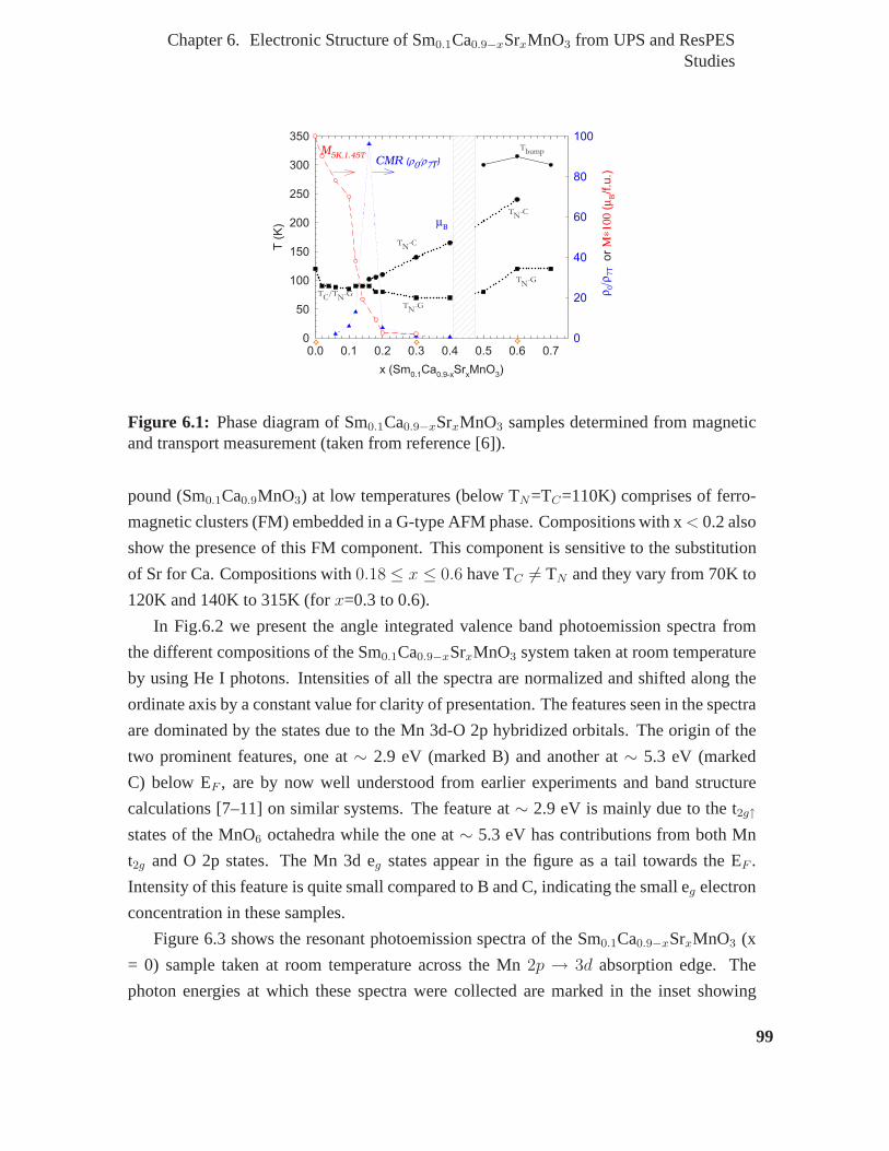
Chapter 6. Electronic Structure of Sm0.1Ca0.9−xSrxMnO3 from UPS and ResPESStudies
x (Sm0.1Ca
0.9-xSr
xMnO
3)
0.0 0.1 0.2 0.3 0.4 0.5 0.6 0.7
T(K)
0
50
100
150
200
250
300
350
ρ0/ρ
7T
0
20
40
60
80
100
TN-G
TN-C
TC/TN-G
� � �
CMR (ρ0/ρ7T)
Tbump
TN-C
TN-G
orΜ∗100(µ
Β/f.u.)
µΒ
M5K,1.45T
Figure 6.1: Phase diagram of Sm0.1Ca0.9−xSrxMnO3 samples determined from magneticand transport measurement (taken from reference [6]).
pound (Sm0.1Ca0.9MnO3) at low temperatures (below TN=TC=110K) comprises of ferro-
magnetic clusters (FM) embedded in a G-type AFM phase. Compositions with x< 0.2 also
show the presence of this FM component. This component is sensitive to the substitution
of Sr for Ca. Compositions with0.18 ≤ x ≤ 0.6 have TC 6= TN and they vary from 70K to
120K and 140K to 315K (forx=0.3 to 0.6).
In Fig.6.2 we present the angle integrated valence band photoemission spectra from
the different compositions of the Sm0.1Ca0.9−xSrxMnO3 system taken at room temperature
by using He I photons. Intensities of all the spectra are normalized and shifted along the
ordinate axis by a constant value for clarity of presentation. The features seen in the spectra
are dominated by the states due to the Mn 3d-O 2p hybridized orbitals. The origin of the
two prominent features, one at∼ 2.9 eV (marked B) and another at∼ 5.3 eV (marked
C) below EF , are by now well understood from earlier experiments and band structure
calculations [7–11] on similar systems. The feature at∼ 2.9 eV is mainly due to the t2g↑
states of the MnO6 octahedra while the one at∼ 5.3 eV has contributions from both Mn
t2g and O 2p states. The Mn 3d eg states appear in the figure as a tail towards the EF .
Intensity of this feature is quite small compared to B and C, indicating the small eg electron
concentration in these samples.
Figure 6.3 shows the resonant photoemission spectra of the Sm0.1Ca0.9−xSrxMnO3 (x
= 0) sample taken at room temperature across the Mn2p → 3d absorption edge. The
photon energies at which these spectra were collected are marked in the inset showing
99
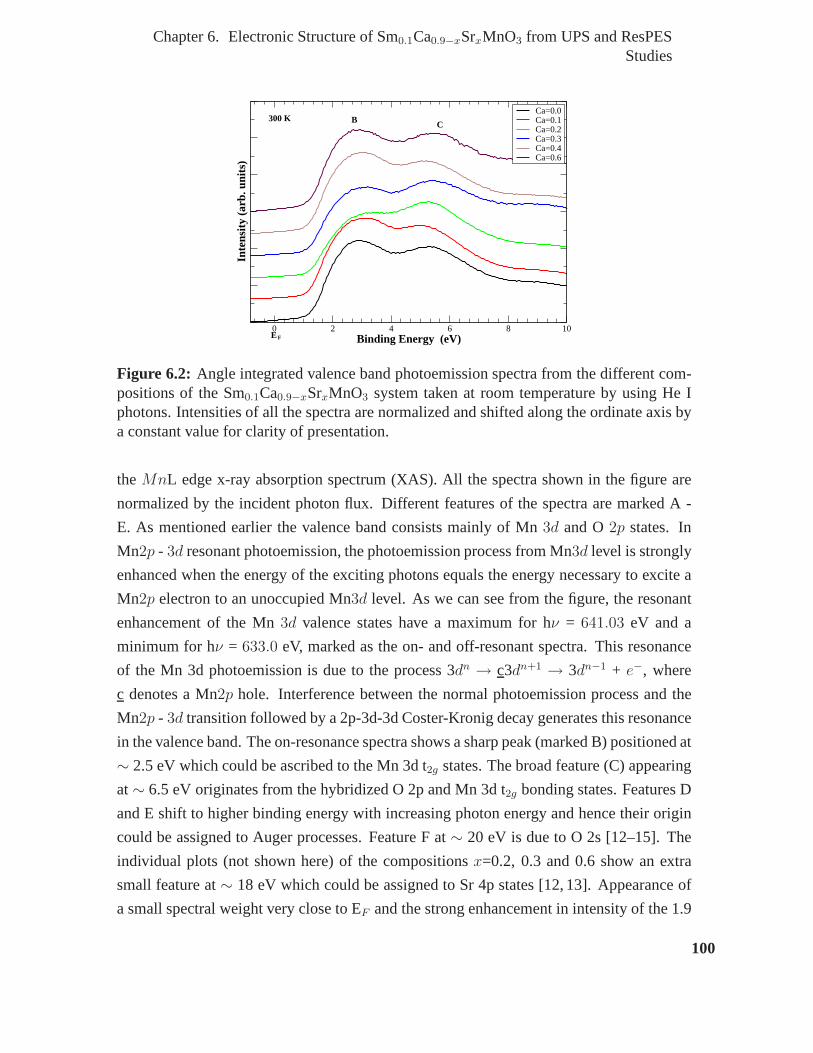
Chapter 6. Electronic Structure of Sm0.1Ca0.9−xSrxMnO3 from UPS and ResPESStudies
0 2 4 6 8 10Binding Energy (eV)
Inte
nsity
(ar
b. u
nits
)
Ca=0.0Ca=0.1Ca=0.2Ca=0.3Ca=0.4Ca=0.6
300 K B C
EF
Figure 6.2: Angle integrated valence band photoemission spectra from the different com-positions of the Sm0.1Ca0.9−xSrxMnO3 system taken at room temperature by using He Iphotons. Intensities of all the spectra are normalized and shifted along the ordinate axis bya constant value for clarity of presentation.
theMnL edge x-ray absorption spectrum (XAS). All the spectra shown in the figure are
normalized by the incident photon flux. Different features of the spectra are marked A -
E. As mentioned earlier the valence band consists mainly of Mn 3d and O2p states. In
Mn2p - 3d resonant photoemission, the photoemission process from Mn3d level is strongly
enhanced when the energy of the exciting photons equals the energy necessary to excite a
Mn2p electron to an unoccupied Mn3d level. As we can see from the figure, the resonant
enhancement of the Mn3d valence states have a maximum for hν = 641.03 eV and a
minimum for hν = 633.0 eV, marked as the on- and off-resonant spectra. This resonance
of the Mn 3d photoemission is due to the process 3dn → c3dn+1 → 3dn−1 + e−, where
c denotes a Mn2p hole. Interference between the normal photoemission process and the
Mn2p - 3d transition followed by a 2p-3d-3d Coster-Kronig decay generates this resonance
in the valence band. The on-resonance spectra shows a sharp peak (marked B) positioned at
∼ 2.5 eV which could be ascribed to the Mn 3d t2g states. The broad feature (C) appearing
at∼ 6.5 eV originates from the hybridized O 2p and Mn 3d t2g bonding states. Features D
and E shift to higher binding energy with increasing photon energy and hence their origin
could be assigned to Auger processes. Feature F at∼ 20 eV is due to O 2s [12–15]. The
individual plots (not shown here) of the compositionsx=0.2, 0.3 and 0.6 show an extra
small feature at∼ 18 eV which could be assigned to Sr 4p states [12, 13]. Appearance of
a small spectral weight very close to EF and the strong enhancement in intensity of the 1.9
100

Chapter 6. Electronic Structure of Sm0.1Ca0.9−xSrxMnO3 from UPS and ResPESStudies
630 640 650 660 670Photon energy (eV)
Inte
nsity
(ar
b. u
nit)
05101520Binding energy (eV)
Inte
nsity
(ar
b. u
nit)
633 (off res)
634.97
637
637.90
638.05
638.51
638.80
639.24
640.14
640.58
641.03 (on res)
642.07
643
644
diff.spectrum
Mn 2p-3d
23L L
XAS (300K)
A
BCD
EF
hν(eV)
Figure 6.3: Valence band resonant photoemission spectra of Sm0.1Ca0.9−xSrxMnO3 forx = 0.0 composition. In the inset theMnL edge x-ray absorption spectrum (XAS) isshown. The photon energies used to probe the resonant valence band are marked by blackcircles in the XAS spectrum. Off- and on- resonance spectra are mentioned. Various peaksappearing in the on-resonance spectrum have been indicatedby A, B, C, D, E and F respec-tively.
eV feature indicate that Mn 3d states give a significant contribution to the valence band of
Sm0.1Ca0.9MnO3. The sharp feature at 6 eV indicates the existence of strong Mn3d-O2p
hybridization in the valence band regime. The very weak spectral weight (feature A) around
Fermi energy in the resonant photoemission spectrum could be attributed to low density of
eg electrons in Sm0.1Ca0.9−xSrxMnO3; having only a small fraction of Mn3+ (t32ge1g) ions.
In figure 6.4 we present the Mn3d spectra from the Sm0.1Ca0.9−xSrxMnO3 samples.
These spectra were obtained by subtracting the corresponding off-resonant spectra from
the on-resonant spectra obtained from the different compositions. The difference spectrum
is expected to resemble the Mn 3d partial density of states. As can be seen from the figure,
there are significant spectral changes with increase in the Sr doping. The states coming
from the Mn 3d eg band do not show any shift in binding energy positions or a change in
spectral intensity. This behaviour is consistent with its electrical transport measurements
which showed that the room temperature resistivity values of various compositions (x) have
almost the same order of magnitude. For x=0.2, the Mn t2g peak shows a shift towards the
lower binding energy. This shift indicates a change in the Mn-O-Mn hybridization strength.
101

Chapter 6. Electronic Structure of Sm0.1Ca0.9−xSrxMnO3 from UPS and ResPESStudies
051015Binding energy (eV)
Inte
nsity
(ar
b. u
nit)
x=0.0
x=0.2
x=0.3
x=0.4
x=0.6
EF
Figure 6.4: The difference spectra obtained from the on and off resonance spectra corre-sponding to the compositionsx=0.2, 0.3, 0.4 and 0.6 are shown. The spectra have beengiven constant shifts along y-axis for clarity of presentation.
As strontium content is raised, the A site cation size increases. Ionic radii of Sr2+ is 132
pm while Ca2+ is 114 pm. Increase in cation size could be leading to a decrease in the
distortion of the MnO6 octahedra and straightening of Mn-O-Mn bond angle. This results
in an increase in Mn 3d - O 2p hybridization. Hence Mn t2g peak shifts towards Fermi
energy. For higher doping like x= 0.3 and 0.4, the size mismatch could be detrimental
to the Mn-O-Mn bond angle and the Mn 3d - O 2p hybridization [6]. Therefore despite
the increase in Sr, the Mn-O-Mn bond angle decreases and thisreduces the Mn 3d - O
2p hybridization. Dalai et al. [7] have reported in a recent paper that the electron-doped
compound Ca0.86Pr0.14MnO3 shows a transfer of some of the electrons from the t2g states to
eg states due to the reduced crystal field splitting in the FMM phase. The low temperature
ground state of this compound also comprises of phase separated FMM and AFMI clusters.
The observed shift in the t2g states in our Sm0.1Ca0.9−xSrxMnO3 samples could also indicate
a similar weakening of the crystal field splitting in compositions with x≤ 0.2 following the
structural changes in the MnO6 octahedra.
102

Chapter 6. Electronic Structure of Sm0.1Ca0.9−xSrxMnO3 from UPS and ResPESStudies
6.4 Conclusions
We have studied the valence electronic structure of the electron-doped CMR material
Sm0.1Ca0.9−xSrxMnO3 for x=0.0, 0.2, 0.3, 0.4 and 0.6 using ultra violet photoelectronspec-
troscopy (UPS) and resonance photoelectron spectroscopy (ResPES) with varying photon
energy across the Mn 2p-3d absorption edge. The magnetic ground state of the parent
compound (Sm0.1Ca0.9MnO3) at low temperatures consists of ferromagnetic clusters (FM)
embedded in a G-type AFM phase. But this FM component is very sensitive to the substitu-
tion of Sr for Ca. The combined UPS and ResPES studies suggestthat the valence band of
this material has major contribution from Mn 3d states and there is a strong hybridization
between Mn 3d t2g and O 2p states. With strontium doping, the A site cation sizeincreases
and a significant change in the Mn 3d spectral weight is observed, indicating that there is a
change in Mn 3d - O 2p hybridization strength due to structural modification caused by Sr
doping.
103

Bibliography
[1] A. Maignan, C. Martin, F. Damay, B. Raveau and J. Hejtmanek, Physical Review B
58, 2758 (1998).
[2] C. Martin, A. Maignan, M. Hervieu and B. Raveau, PhysicalReview B60, 12191
(1999).
[3] Adriana Moreo, Matthias Mayr, Adrian Feiguin, Seiji Yunoki, and Elbio Dagotto,
Phys. Rev. Lett.84, 5568 (2000).
[4] Adriana Moreo, Seiji Yunoki, Elbio Dagotto, Science283, 2034 (1999).
[5] C. Martin, A. Maignan, M. Hervieu, B. Raveau, Z. Jirák, M.M. Savosta, A. Kurbakov,
V. Trounov, G. André, F. Bourée, Physical Review B62, 6442 (2000).
[6] C. Martin, A. Maignan, M. Hervieu, S. Hébert, A. Kurbakov, G. André, F. Bourée-
Vigneron, J. M. Broto, H. Rakoto, and B. Raquet, Physical Review B 77, 054402
(2008).
[7] M. K. Dalai, P. Pal, B. R. Sekhar, M. Merz, P. Nagel, S. Schuppler and C. Martin,
Physical Review B85, 155128 (2012).
[8] P. Pal, M. K. Dalai, R. Kundu, and B. R. Sekhar, Physical Review B 77, 184405
(2008).
[9] P. Pal, M. K. Dalai, B. R. Sekhar, I. Ulfat, M. Merz, P. Nagel, S. Schuppler, Physica
B 406, 3519-3523 (2011).
[10] M. Chakraborty, P. Pal, and B. R. Sekhar, Solid State Commun.145, 197, (2008).
[11] T. Saitoh, A. E. Bocquet, T. Mizokawa, H. Namatame, A. Fujimori, M. Abbate, Y.
Takeda and M. Takano, Physical Review B51, 13942 (1995).
[12] F. L. Battye, H. Höchst and A. Goldmann, Solid State Communications19, 269-271
(1976).
[13] B. Reihl, J. G. Bednorz, K. A. Müller, Y. Jugnet, G. Landgren and J. F. Morar, Physical
Review B30, 803 (1984).
[14] P. Pertosa and F. M. Michel-Calendini, Physical ReviewB 17, 2011 (1978).
104

Bibliography
[15] M. Kowalik, R. Zalecki and A. Kolodziejczyk, Acta Physica Polanica A117, 277
(2010).
105

7Summary
In this thesis, the electronic structures of single crystalgraphite and highly oriented py-
rolytic graphite have been studied using ARPES, KRIPES and band structure calculations.
The electronic structures of single layer graphene and bilayer graphene have also been in-
vestigated using tight binding calculations. Further, theoccupied electronic structures of
Pb doped multiferroic material, (Bi1−xPbxFeO3) and Sr doped Sm0.1Ca0.9MnO3 (a colossal
magnetoresistive material) have been studied using UPS, XPS and ResPES techniques.
Using ARPES, we have studied the valence band structure of natural single crystal
graphite along the symmetry directionsΓK andΓM of its brillouin zone. We find two
clearly dispersing bands (π andσ) in both the directions. We observe that the agreement of
our results is good near the zone boundaries (theK andM points) with the calculated band
structure for which interactions of electrons up to third nearest neighbours are considered
and near the zone centre (theΓ point) the agreement is better with the calculated bands
having first nearest neighbour interaction only. In HOPG thevalence band dispersions
were taken along different radial directions of its Brillouin zone and we found no azimuthal
dependence of the spectra as expected. We estimated a splitting of ∼ 0.5 eV between the
two valenceπ bands of single crystal graphite from its near Fermi energy spectra at theK
point. This splitting is due to the weak interlayer couplingin graphite. We also observe
the appearance of a sharp peak below EF at theK point at low temperature which comes
up due to coupling of electrons with phonon, indicating a strong electron-phonon coupling.
In HOPG we see only a singleπ band feature near the Fermi energy at its zone boundary.
The inherent azimuthal disorder of HOPG makes it difficult toresolve the twoπ bands
at the zone boundary. To study the conduction band structureof HOPG along a radial
direction of its circular Brillouin zone and that of a singlecrystal graphite along a direction,
106

Chapter 7.Summary
slightly away from theΓM symmetry direction, we have used KRIPES. We see that for
both the systems, the results superimpose on the theoretical conduction band structure of
graphite alongΓM direction. In order to calculate the band structure of threedimensional
graphite we have first constructed a formalism for the electronic structure calculation of
single layer graphene, developed the method for bilayer graphene including up to third
nearest neighbour interactions and finally applied it on graphite. From the calculations
on graphene we have got a set of tight binding parameters on the physical ground that the
absolute values of the parameters should decrease as one moves from first nearest neighbour
towards higher distance. This set of parameters has been used to see the effect of in-plane
first nearest neighbour overlap integral, second and third nearest neighbour interactions on
the band structure of bilayer graphene. We have also illustrated the role of site energy
difference (∆) between A and B sublattices in the same graphene layer on theelectronic
spectra of bilayer graphene. The Sublattice asymmetry in monolayer graphene introduces
a gap in the spectra at theK point whereas in bilayer it gives an asymmetry in the energy
values of the top valence and bottom conduction bands with respect to the energy at which
the other two bands are degenerate. The different in-plane parameters also induce electron-
hole asymmetry in the slope of the valence and conduction bands. The effects of these
parameters are similar, on graphite at theK point, to those of bilayer graphene but at the
H point a gap opens up due to∆.
Further, we have studied the valence band electronic structure of the Bi1−xPbxFeO3
(x = 0.02 to 0.15) system by using X-ray and ultra-violet photoelectron spectroscopy. As
this system undergoes a R3c to cubic phase transition with Pbdoping, the near Fermi level
states show an enhanced oxygen 2p character due to the weakening of the Fe 3d - O 2p
- Bi 6p hybridization strength. The valence bands of compositions with the R3c structure
were found to be qualitatively similar to the LSDA calculations except for their estimates
of the band width and band gap. Reasons for this could be the higher value of the effective
Coulomb interaction. These results could be of importance to the understanding of the
electron-electron correlation in multiferroic materials.
Finally, we have studied the electronic structure of Sm0.1Ca0.9−xSrxMnO3 (x=0.0, 0.2,
0.3, 0.4 and 0.6) system, an electron-doped CMR material using ultra violet photoelectron
spectroscopy (UPS) and resonance photoelectron spectroscopy (ResPES) with varying pho-
ton energy across the Mn 2p-3d absorption edge. The magneticground state of the parent
compound (Sm0.1Ca0.9MnO3) at low temperatures consists of ferromagnetic clusters (FM)
embedded in a G-type AFM phase. But this FM component is very sensitive to the substi-
107

Chapter 7.Summary
tution of Sr for Ca. From the combined UPS and ResPES studies we find that the valence
band of this material has major contribution from Mn 3d states and a strong hybridization
is there between Mn 3d t2g and O 2p states. With strontium doping, the A site cation size
increases and a significant change in the Mn 3d spectral weight is observed which indicates
that there is a change in Mn 3d - O 2p hybridization strength due to structural modification
caused by Sr doping.
Regarding the first part of this thesis, i.e., the electronicstructure study of graphite,
it could be noted that though the system has been studied earlier quite a bit, many of its
modified forms like intercalated and irradiated graphite might display interesting physics
if reinvestigated using the advanced experimental facilities that are available in the present
day. On the other hand, the transition metal oxides need a lotmore studies for a better
understanding of their complex physical properties.
108