Electronic Spin Transport and Thermoelectric E ects in ... · Graphene Graphene, a two dimensional...
145
Phd Thesis Doctoral Program in Physics Electronic Spin Transport and Thermoelectric Effects in Graphene Ingmar Neumann Thesis Director Prof. Sergio O. Valenzuela Tutor Prof. Jordi Pascual i Gainza Institut Catal` a de Nanotecnologia Universitat Aut` onoma de Barcelona Bellaterra, 2014
Transcript of Electronic Spin Transport and Thermoelectric E ects in ... · Graphene Graphene, a two dimensional...

Phd ThesisDoctoral Program in Physics
Electronic Spin Transport and
Thermoelectric Effects in Graphene
Ingmar Neumann
Thesis Director
Prof. Sergio O. Valenzuela
Tutor
Prof. Jordi Pascual i Gainza
Institut Catala de Nanotecnologia
Universitat Autonoma de Barcelona
Bellaterra, 2014


Fur meine Eltern


Contents
1. Introduction 1
2. Theoretical Background 52.1. Introduction . . . . . . . . . . . . . . . . . . . . . . . . . . . . . . . . . 52.2. Electrical and Thermal Conduction in Metals . . . . . . . . . . . . . . 52.3. Magnetism in Solid State Physics and Electronics . . . . . . . . . . . . 7
2.3.1. Stoner Wolfarth Model . . . . . . . . . . . . . . . . . . . . . . . 72.3.2. Magnetoresistance . . . . . . . . . . . . . . . . . . . . . . . . . 8
2.4. Spin Accumulation . . . . . . . . . . . . . . . . . . . . . . . . . . . . . 92.5. Non Local Spin Injection and Detection . . . . . . . . . . . . . . . . . . 12
2.5.1. Motivation . . . . . . . . . . . . . . . . . . . . . . . . . . . . . . 122.5.2. System . . . . . . . . . . . . . . . . . . . . . . . . . . . . . . . . 122.5.3. Derivation of the Diffusion Equation . . . . . . . . . . . . . . . 142.5.4. Interfacial Currents . . . . . . . . . . . . . . . . . . . . . . . . . 152.5.5. Spin Dependent Voltage . . . . . . . . . . . . . . . . . . . . . . 16
2.6. Hanle Spin Precession . . . . . . . . . . . . . . . . . . . . . . . . . . . 182.7. Spin Caloritronics . . . . . . . . . . . . . . . . . . . . . . . . . . . . . . 202.8. Graphene . . . . . . . . . . . . . . . . . . . . . . . . . . . . . . . . . . 23
2.8.1. Introduction . . . . . . . . . . . . . . . . . . . . . . . . . . . . . 232.8.2. Band Structure of Graphene in the Tight Binding Approach . . 232.8.3. The Electric Field Effect . . . . . . . . . . . . . . . . . . . . . . 262.8.4. Mobility . . . . . . . . . . . . . . . . . . . . . . . . . . . . . . . 29
2.9. Spin Relaxation in Graphene . . . . . . . . . . . . . . . . . . . . . . . . 302.9.1. Introduction . . . . . . . . . . . . . . . . . . . . . . . . . . . . . 302.9.2. Elliot-Yafet Spin Relaxation . . . . . . . . . . . . . . . . . . . . 312.9.3. D‘yakonov-Perel Spin Relaxation . . . . . . . . . . . . . . . . . 322.9.4. Comparison between EY and DP Mechanism . . . . . . . . . . . 332.9.5. Experimental Results . . . . . . . . . . . . . . . . . . . . . . . . 342.9.6. Further Mechanisms of Spin Relaxation in Graphene . . . . . . 34
3. Experimental Techniques and Methods 373.1. Introduction . . . . . . . . . . . . . . . . . . . . . . . . . . . . . . . . . 373.2. Fabrication and Characterization of Single Layer Graphene . . . . . . . 37
3.2.1. Mechanical Exfoliation . . . . . . . . . . . . . . . . . . . . . . . 37
V

Contents
3.2.2. Optical Characterization and Raman Spectroscopy . . . . . . . 38
3.2.3. AFM characterization . . . . . . . . . . . . . . . . . . . . . . . 39
3.3. Properties of Crosslinked PMMA . . . . . . . . . . . . . . . . . . . . . 41
3.3.1. Crosslinking PMMA . . . . . . . . . . . . . . . . . . . . . . . . 41
3.3.2. Choosing the Stepsize . . . . . . . . . . . . . . . . . . . . . . . 42
3.3.3. Choosing the Electron Beam Dose . . . . . . . . . . . . . . . . . 44
3.3.4. Creating trenches in overexposed PMMA . . . . . . . . . . . . . 46
3.3.5. Controlling the Height Profile of the Polymer Substrate . . . . . 46
3.4. Fabrication and Engineering of Nanodevices . . . . . . . . . . . . . . . 48
3.4.1. Advantages of Electron Beam Lithography . . . . . . . . . . . . 48
3.4.2. Standard Electron Beam Lithography . . . . . . . . . . . . . . . 50
3.4.3. Graphene spin valve devices . . . . . . . . . . . . . . . . . . . . 50
3.4.4. Using Crosslinked PMMA as a substrate . . . . . . . . . . . . . 52
3.4.5. Suspended Graphene Spin Valves . . . . . . . . . . . . . . . . . 53
3.5. Measurement setup . . . . . . . . . . . . . . . . . . . . . . . . . . . . . 55
3.5.1. Experimental Techniques . . . . . . . . . . . . . . . . . . . . . . 55
3.5.2. Four Point Measurements and the Electric Field Effect . . . . . 56
3.5.3. Non Local Spin Valve Measurements . . . . . . . . . . . . . . . 57
3.5.4. Hanle Measurements . . . . . . . . . . . . . . . . . . . . . . . . 59
3.5.5. Equipment . . . . . . . . . . . . . . . . . . . . . . . . . . . . . . 59
4. On the Theory of Spin Dependent Tunneling 614.1. Introduction . . . . . . . . . . . . . . . . . . . . . . . . . . . . . . . . . 61
4.2. Free Electron Tunneling . . . . . . . . . . . . . . . . . . . . . . . . . . 63
4.3. Discussion . . . . . . . . . . . . . . . . . . . . . . . . . . . . . . . . . . 67
4.4. Conclusion . . . . . . . . . . . . . . . . . . . . . . . . . . . . . . . . . . 69
5. Electrical Detection of Spin Precession in freely-suspended Graphene SpinValves 715.1. Introduction . . . . . . . . . . . . . . . . . . . . . . . . . . . . . . . . . 71
5.2. Spin Injection in Graphene . . . . . . . . . . . . . . . . . . . . . . . . . 71
5.3. Results and Discussion . . . . . . . . . . . . . . . . . . . . . . . . . . . 73
5.4. Conclusion . . . . . . . . . . . . . . . . . . . . . . . . . . . . . . . . . . 77
6. Enhanced Spin Accumulation in Graphene Spin Valves 796.1. Introduction . . . . . . . . . . . . . . . . . . . . . . . . . . . . . . . . . 79
6.2. Motivation . . . . . . . . . . . . . . . . . . . . . . . . . . . . . . . . . . 79
6.3. Amorphous Carbon as Interface Material . . . . . . . . . . . . . . . . . 81
6.4. Experimental Results and Discussion . . . . . . . . . . . . . . . . . . . 83
6.5. Conclusion . . . . . . . . . . . . . . . . . . . . . . . . . . . . . . . . . . 87
VI

Contents
7. Spin Thermocouple and Giant Spin Accumulation in Single Layer Graphene 897.1. Introduction . . . . . . . . . . . . . . . . . . . . . . . . . . . . . . . . . 897.2. General Concept . . . . . . . . . . . . . . . . . . . . . . . . . . . . . . 89
7.2.1. Context . . . . . . . . . . . . . . . . . . . . . . . . . . . . . . . 897.2.2. Graphene NLSV as Spin Thermocouple . . . . . . . . . . . . . . 91
7.3. Experimental Results . . . . . . . . . . . . . . . . . . . . . . . . . . . . 937.3.1. Device Characteristics . . . . . . . . . . . . . . . . . . . . . . . 937.3.2. Non Local IV Measurements . . . . . . . . . . . . . . . . . . . . 947.3.3. Analysis of the Data . . . . . . . . . . . . . . . . . . . . . . . . 987.3.4. Hot Carriers . . . . . . . . . . . . . . . . . . . . . . . . . . . . . 101
7.4. Conclusion . . . . . . . . . . . . . . . . . . . . . . . . . . . . . . . . . . 103
8. Conclusions 105
9. Acknowledgements 109
A. List of Publications 113
B. Supplementary Material to Chapter 7 115B.1. Numerical Simulation of the Temperature Profile . . . . . . . . . . . . 115B.2. Non Local and Thermoelectric Voltage . . . . . . . . . . . . . . . . . . 117B.3. Temperature obtained via Mott Relation . . . . . . . . . . . . . . . . . 118B.4. Spin Dependent Seebeck Coefficients . . . . . . . . . . . . . . . . . . . 119
C. Recipes for the sample fabrication 121
D. List of Abbreviations 125
Bibliography 125
VII


1. Introduction
Solid state physics and electronics are historically closely related. One could say thatadvances in solid state physics are a requirement for new developments in electronics.The invention of the transistor in 1947 is a prime example for that. Without thedevelopment of the band structure theory of solids, the experimental realization ofthe transistor would not have been possible. In retrospect, it is safe to say that fewinventions of the 20th century have influenced our society so thoroughly to the presentday.
Throughout the last 50 years, progress in the semiconductor and information storageindustry was mainly due to a miniaturization of the transistors and integrated circuits.However, nowadays the industry is facing a paradigm shift, as typical dimensions ofthe electronical components are approaching a limit where quantum mechanical effectsstart to play an important role.
Therefore, alternatives to traditional electronics will become necessary in the future.Again, an understanding of elementary physics is a prerequisite for the engineering ofnovel nanotechnological devices based on completely new concepts.
Two fields that could provide such alternatives are spintronics and graphene physics.Both are among the currently most active areas of solid state physics, which is ex-pressed in the fact that in recent years, two nobel prizes have been awarded for dis-coveries in these fields. The numbers of publications concerning graphene is stillexponentially increasing year after year, and also spintronics has seen a number ofsignificant advances recently, which include effects such as the spin Hall effect or spintorque physics.
The aim of this thesis is to investigate spin and heat currents in graphene. Besidesgraphene and spintronics, it is also related to spin caloritronics, which is another areaenjoying rapid growth.
While the search for new applications and technologies is important from a prac-tical point of view, we hope to demonstrate that the work presented in this thesisconstitutes a piece of research, which is justified in itself by shedding light on new andexciting physics.
Spintronics
In contrast to electronics, which relies solely on the charge of the electron, the ideaof spintronics is to also use its spin in order to build micro- and nanotechnologicaldevices with enhanced perfomance or novel functionalities.
1

1. Introduction
Between 1971 and 1973, Tedrow and Meservey demonstrated that spin polarizedelectrons can exist outside of a ferromagnet [1, 2]. They used the Zeeman split-ting of a superconductor to detect the spin polarization of a tunneling current insideof a Ferromagnet/Insulator/Superconductor (FM/I/SC) junction. Two years later,Julliere demonstrated that it was possible to use the exchange splitting of a secondFerromagnet instead of the Zeeman splitted superconductor, leading to the discoveryof tunneling magnetoresistance (TMR) in FM/I/FM junctions [3]. Finally, over adecade later giant magneto resistance (GMR) was discovered in multi layered struc-tures by Grunberg and Fert in two indepedent pieces of research [4, 5], winning themthe Nobel prize in physics in 2007.
Although closely related to TMR and GMR, the work presented in this thesis be-longs to a second branch of research motivated by the Tedrow/Meservey experiments.Building on their pioneering work, Aronov and Pikus suggested in 1976 that it wouldbe possible to create non equilibrium spin polarization in a non magnetic material bypassing a current through a ferromagnet [6, 7]. Experimental evidence was first givenby Johnson and Silsbee from 1985 on [8, 9, 10]. They experimentally demonstratedelectrical spin injection using a non local geometry, which separates spin and chargecurrents.
In 2001, Jedema et al. demonstrated electrical spin injection at room temperatureusing a similar structure as Johnson and Silsbee [11]. Due to advances in nanolithog-raphy methods, they had been able to reduce the size of their samples three orders ofmagnitude, increasing the non local voltages for the same amount.
Following these experiments, a variety of spin related effects in solid state media hasbeen discovered, such as the inverse spin Hall effect[12] or spin transfer torque[13, 14].For a more detailed explanation of these fascinating phenomena, the reader is referredto ref. [15], which is a comprehensive review of spintronics and its applications, whilethe evolution of local techniques is described in detail in ref. [16].
Graphene
Graphene, a two dimensional system of carbon in a honeycomb lattice is one ofthe most promising materials for electronics, but also spintronics. The theoreticalproperties of graphene have been studied as early as 1947 [17]. However, until theseminal paper of Novoselov, Geim et al. in 2004 [18], experimental studies of graphenewere scarce. Not only did they demonstrate that it was possible to obtain graphene bypeeling off single layers from a bulk of graphite by simple Scotch tape, they did alsoshow that those layers are visible in an optical microscope due to an interference effectwith the substrate, which made the study of graphene straightforward and widelyavailable. This contributed to the exponential increase in graphene related researchactivity. Geim and Novoselov were awarded with the Nobel prize in physics in 2010.
Graphene offers unique and exciting physics to study. Moreover, it exhibits superiormaterial properties, such as electric and thermal conductivity, mechanical flexibility or
2
ultra-high electronic mobilities. These properties make it a potential building block ofthe next disruptive technology [19], and initially many efforts were put into realizinggraphene based transistors, in order to replace Silicon as the abundant electronic mate-rial. However, the likelihood of this seem increasingly small. Instead, new applicationsfor graphene are sought for, which exploit its excellent material qualities.
The spin injection measurements presented throughout this thesis underline thepotential of graphene in the context of spintronics, but also the complexity and broadphysical effects that can be studied with this material, such as novel ways to control theelectronic spin. Charge transport studies have benefited considerably of the fabricationof freely suspended devices, which allow for the investigation of graphene undisturbedby the substrate. Similar benefits can be expected in the context of spin transportstudies, and in order to gain insight into the relationship between mobility and spinrelaxation lenght, we have developed a method to fabricate freely suspended graphenespin valves, which we present in chapter 5. Moreover, we have demonstrated thatthe spin injection efficiency in graphene can be greatly enhanced by the deposition ofa thin layer of amorphous carbon at the FM/graphene interface. These results arepresented in chapter 6.
For further reading, ref. [20] discusses the electronic properties of graphene, ref. [21]the experimental ones, while the search for applications is summarized in ref. [19]. Areview of spintronics in graphene is ref. [22].
Spin Caloritronics
The field of spin caloritronics is relatively new. It came to attention due to a renewedinterest in classical thermoelectrical effects known and studied since the 1800s, suchas the Seebeck effect. In spin caloritronics, spin dependent versions of these classicaleffects are investigated on a mesoscopic scale.
Massive interest in the interplay between heat and spin currents has been triggeredby the observation of the so-called spin Seebeck effect in 2008 [23]. This motivatedthe exploration of similar and related effects, such as the spin-dependent Seebeckeffect, or the magneto Seebeck effect, the spin dependent Peltier effect [24]. Our owngroup has contributed to the topic with the experimental realization of a magnon-dragthermopile [25].
It is intriguing to explore the possibility of spin caloritronics in graphene. Consider-able efforts have been taken in order to investigate the thermal properties of graphene,such as thermal conductivity [26] or its Seebeck coefficient [27]. As we demonstrate inchapter 7, the interplay of spin and heat currents in graphene allows for the realizationof novel devices which we descibe as a spin thermocouple.
An excellent review of spin caloritronics is ref. [24], while the thermal properties ofgraphene are summarized in ref. [28].
Contents of this thesis
3

1. Introduction
The structure of this thesis is as follows:
• In chapter 2, we introduce basic theoretical concepts required for the interpre-tation of the experiments presented throughout this thesis. We focus on spininjection into non magnetic materials, discussing topics such as spin accumula-tion or the phenomenological model of spin injection. These concepts can easilybe applied to spin injection into graphene. We conclude the chapter with adiscussion of spin relaxation in graphene.
• In chapter 3, we describe the fabrication process of our devices, including adetailed description of the mechanical exfoliation of graphene as well as thecharacterization of crosslinked PMMA. We further discuss the different processesused for the device fabrication and explain basic measurement configurations aswell as the equipment used during fabrication and measurements.
• Chapter 4 consists of a theoretical study of the spin polarization of electronstunneling between ferro- and non magnetic material. The model allows us tostudy electronic tunneling more thoroughly, and to introduce basic conceptsregarding spin dependent electronic transport.
• In chapter 5, we demonstrate succesful electrical spin injection into freely sus-pended graphene spin valves. These devices are fabricated using an acid freemethod developed in the context of this thesis, where we use crosslinked PMMAin order to suspend the graphene flake. Moreover, we demonstrate Hanle spinprecession in our devices, yielding a spin relaxation length of approx. 1.8µm.These results have been published in Small.
• In chapter 6 we discuss how we obtain enhanced non local voltages in our spinvalve devices by an additional step during the fabrication process. The resultsof this chapter have been published in Applied Physics Letters.
• In chapter 7 we present measurements of giant spin accumulation in graphene.This is due to the enhanced signal in the non local spin valves and a further en-hancement due to a second order contribution of the bias current. We show thatat the Dirac point of graphene, the device can be seen as a spin thermocouple,where the two arms are formed by the spin channels. These results are currentlyin preparation for submission to a scientific journal.
• The main results of this thesis are summarized in chapter 8.
• Supplementary material regarding chapter 7, recipes for the device fabrication,as well as a list of publications and a list of abbreviations are given in theappendix.
4

2. Theoretical Background
2.1. Introduction
The experimental work presented in this thesis is related to several areas of cur-rently active research in solid state physics, such as spintronics, spin caloritronics andgraphene. Therefore, this theorectical chapter has to cover a wide range of differenttopics. The aim of this chapter is to introduce basic principles of each topic, providinga basis for the understanding of the work presented in the later sections of this thesis.
The layout of this chapter is as follows:
We start with a brief introduction to the classic theory of electronic and thermalconduction in metals, including a description of the Seebeck effect (section 2.2).
Then, we discuss the theory of magnetism in solid state physics, especially theStoner Wolfarth model of ferromagnetism, the two-current model of Mott and magne-toresistance (section 2.3). Then, we introduce the concept of spin accumulation in nonmagnetic materials (section 2.4). We also present a detailed description of the stan-dard model of spin injection into non magnetic materials (section 2.5), and introduceHanle spin precession (section 2.6).
We then give a basic introduction to the newly emerging field of spin caloritronics(section 2.7). Here, we make the attempt to show the formal similarity between thedifferent types of transport, be it charge, heat or spin current.
Finally, we discuss basic properties of graphene such as the electronic band structureand the electric field effect (section 2.8). An introduction to spin relaxation in grapheneconcludes the chapter (section 2.9).
2.2. Electrical and Thermal Conduction in Metals
Electrical and thermal transport in metals can be understood within a semi-classicalmodel similar to the kinetic gas theory, the Drude model [29, 30, 31]. According tothis model, conduction is mediated by scattering events between the valence electronsand the ions of the metals. This defines the mean free path of the electrons λe as wellas the mean free time τe between scattering events.
The DC conductivity σ of a metal is related to the electric field ~E by Ohm´s rule[32] ~jc = σ ~E, where ~jc the charge current density. The index c stands for charge.
5

2. Theoretical Background
Using the electrical potential V and ~E = −∇V , it can be written as
~jc = −σ∇V (2.1)
Hence, a charge current within a metal is caused by a gradient in an electrical potential.In a similar way, a heat current within a metal is caused by a gradient in tempera-
ture, as expressed by Fourier´s rule
~jh = −κ∇T (2.2)
Here, the index h stands for heat, while κ is the thermal conductivity and ∇T a gradi-ent in temperature. The similarity between the two types of conduction is illustratedin Fig. 2.1 (a) and (b), while we introduce the spin current, shown in (c), in section2.4. All types of conduction are examples of diffusive transport.
Figure 2.1.: Conduction of (a) charge, (b)heat and (c) spin currents inmetals
As heat and charge currents in metalsare both dominated by the electrons, aninterplay between the two types of conduc-tion exists. It manifests itself in thermo-electric effects such as the Seebeck effect,which is highly important for the under-standing of the measurements presented inchapter 7. If a temperature gradient is ap-plied to a metal bar, as shown in Fig. 2.1(b), electrons travel from the hot to thecold end of the rod. The resulting ther-moelectric field builds up until it compen-sates for the thermal gradient. This is theSeebeck effect, which can be written as
~E = −S∇T (2.3)
Here, S is the Seebeck coefficient of thematerial. It can be expressed as [33]
S = −π2k2BT
3|e|1
σ
∂σ
∂E|E=EF
(2.4)
Equation 2.4 is the so-called Mott relationor Mott formula of the Seebeck coefficient.
For systems such as graphene, where the Fermi energy EF can be tuned by applyinga gate voltage Vg over a capacitance Cg, S can be written as [27]
S = −π2k2BT
3|e|1
σ
∂σ
∂Vg
∂Vg∂E|E=EF
(2.5)
6

2.3. Magnetism in Solid State Physics and Electronics
where
∂Vg∂EF
=
√|e|Cgπ
2
~vF
√|∆Vg| (2.6)
with the Fermi velocity vF and ∆Vg = Vg − VD. VD is the Dirac point of graphene. Adetailed description of graphene is given in section 2.8.
The interplay between charge, heat and also spin currents has recently receivedrenewed attention by the solid state physics community. The field is labeled SpinCaloritronics [24], which is treated in section 2.7.
2.3. Magnetism in Solid State Physics and Electronics
2.3.1. Stoner Wolfarth Model
Many electronical properties of solid state materials can be explainded using a bandstructure model [29]. These bands can be derived from the atomic configuration ofthe crystal lattice of the material.
Similarly, also ferromagnetism can be understood using a band structure model, theStoner Wolfarth model of ferromagnetism [34]. Within this model, the d band of the3d transition metals Ni, Co and Fe is split into two spin subbands.
Figure 2.2.: (a) Ideal Stoner FM with one filled subband (b) Stoner FM with twopartially filled subbands (c) Nonmagnetic material with two equally filledsubbands
The densities of states (DOS) of an ideal Stoner Ferromagnet (FM) are shown inFig. 2.2 (a). We label the majority spins as spin down and the minority as spin up,without loss of generality. The bottom of their bands are shifted in respect to each
7
2. Theoretical Background
other by Eex. The spin down band is completely filled, as it lies below the Fermienergy. This implies that the spin polarization P of such a material is 100 %.
Ferromagnetic alloys have been developed, which act as ideal Stoner FMs, e.g. theoxide La0.6Sr0.33MnO3 (LSMO) [35] or Heusler alloys such as NiMnSb [36]. However,in most ferromagnetic materials, the spin bandstructure consists of two partially filledsubbands, as shown in Fig. 2.2 (b).
Finally, a sketch of a nonmagnetic material (NM) is shown in Fig. 2.2 (c). Here,the electronic properties are dominated by the s electrons, while there is no imbalancebetween the two spin subbands and the spin polarization is zero.
Considering the electrical currents in such materials, we make use of the two-currentmodel of Mott [37, 38]: We assume that the propability of spin-flips during scatteringevents is negligible. This means that electrons of different types of spin do not mixduring scattering processes, i.e. during electrical or thermal conduction. The conduc-tivity σ of a given material can therefore be expressed as a sum of two independentchannels for spin up and spin down, σ = σ↑ + σ↓.
The electrical current in an ideal Stoner FM is completely spin polarized, as onlyspin up particles can participate in the conduction process. If the two subbandsare partially filled, as shown in Fig. 2.2 (b), both subbands contribute to electricalconduction.
2.3.2. Magnetoresistance
A change in the electrical resistance of a material by applying a magnetic field isreferred to as magnetoresistance (MR). There are different kinds of MR, but for thespin valve measurements, introduced in section 2.5, anisotropic magnetoresistance isespecially important, as it might occur as spurious effect. We further introduce tunnelmagnetoresistance, as an example of a (local) spin valve structure.
Anisotropic Magnetoresistance (AMR) In 1857, Lord Kelvin discovered thatthe electrical resitivity of a ferromagnetic strip changes depending on the angle betweenthe magnetization and the direction of the current [39]. AMR is a band structure effect,and the difference between perpendicular and parallel resistivities ρ‖ and ρ⊥ can bederived as
ρ‖ − ρ⊥ = ∆ρ cos2(θ) (2.7)
where θ is the angle between current and magnetization of the FM.
Tunneling Magnetoresistance (TMR) In contrast to AMR, which can be ob-served in a single FM, TMR occurs in FM/I/FM junctions, where I stands for aninsulator. Applying a bias voltage between the two ferromagnets leads to a tunnel-ing current via the insulating layer which depends on the relative orientation of the
8

2.4. Spin Accumulation
magnetizations of the FMs. TMR is historically defined as [3]
TMR :=R↑↓ −R ↑↑
R↑↑(2.8)
where R↑↓ stands for the anti parallel (AP) alignment of the ferromagnet and R↑↑ forthe parallel (P) alignment.
A graphical representation of TMR is shown in Fig. 2.3. As indicated by the arrows,tunneling takes place only between equal types of spin. For parallel (P) alignment,there is the same amount of spin up and spin down states available at the Fermi energy(Fig. 2.3 (a)).
In case of anti parallel (AP) alignment of the FMs, as depicted in Fig. 2.3 themajority spins tunneling out of FM1 have few states available at the Fermi energy inFM2 to tunnel to. For the minority spin, there are many states available to tunnelto, but few electrons in FM1 at the Fermi energy. Therefore, the resistance of thejunction is higher in the anti parallel case.
Figure 2.3.: Graphical representation of TMR
TMR based devices are examples of so-called spin valve structures. A spin valve isa device consisting of at least two ferromagnetic layers, whose resistance changes bychanging the relative magnetization between the layers. Moreover, this orientation ispreserved even if the power supply is switched off.
2.4. Spin Accumulation
In order to investigate magnetic phenomena such as GMR and TMR, there are manyadvantages in using non local devices, where spin and charge current are separated.
9

2. Theoretical Background
A detailed theoretical description of such systems is given in section 2.5. Here, weintroduce the main concepts of electrical spin injection into non magnetic materials.Especially, we demonstrate that an electrical current via a FM/NM interface is asource of spin current [8].
Figure 2.4.: Electrochemical potentials near an FM/NM interface
There is an important consequence of the Stoner model of FM in combination withthe two-current model of Mott. When an electrical current flows from a FM into anNM, the distribution of the current over spin up and spin down has to change [40].This follows from the fact that in the NM the two spin subbands are equal, thus alsothe number n↑,↓ of spins of a given state as well as the conductivities σ↑,↓ for spin upand spin down electrons. In contrast, there is an imbalance in the FM, meaning thatn↑ 6= n↓ and σ↑ 6= σ↓. As the total number of electrons is conserved, this results in aredistribution of spin up and spin down electrons.
We consider a system as schematically shown in Fig. 2.4. An electrical current ~jflows via a rod consisting of an NM and an FM. We choose the lateral dimensions ofthe system to be small, so that we can treat it as one-dimensional. The direction ofthe current is the x axis, with the FM/NM interface at x = 0. The charge currentdensity is given by ~jc = ~j↑ + ~j↓ and the spin current density by ~js = ~j↑ − ~j↓. In thesame way, the electrochemical potentials are given by µ = µ↑ + µ↓ and µs = µ↑ − µ↓.
In the following, we use the index N to indicate parameters of the NM, and F forthose of the FM, as well as ↑, ↓ for spin up and down.
In this system, the gradient of the electrochemical potential in the direction of the
10

2.4. Spin Accumulation
current is given by [40] ∂xµ↑,↓ = −(e/σ↑,↓)j↑,↓. It follows that in the NM
~js = −σNe∇µs (2.9)
where we wrote ∂x as ∇ in order to stress the formal analogy to Eqs. 2.1 and 2.2for charge and heat currents. The three types of transport are shown in Fig. 2.1.Independently of the nature of the current, all are linear responses to a gradient in thea potential. Like charge and heat, spin transport is of diffusive nature and in steadystate the diffusion equation for the potential difference is given by [40]
µs = τsfD∂2xµs (2.10)
where D is the the diffusion constant of the material and τsf the spin relaxation time:If the source of spins is switched off at a given time, then the excess of one type ofspins would decay exponetially with τsf . It becomes clear from Eq. 2.10 that the spinsplitting of the electrochemical potential also decays exponentially with x, i.e. awayfrom the FM/NM interface:
µs ∝ µ(x = 0)e−λsf/x (2.11)
The splitting is the largest at the interface, while far away, µ↑ = µ↓ has to be validfor both materials. This is a so-called spin accumulation close to the interface. Thecharacteristic length scale over which µs decays is the spin relaxation lenght λsf andfrom Eq. 2.10 follows that
λsf =√τsfD (2.12)
The electrochemical potentials µ↑ and µ↓ within both materials are schematicallyshown in Fig. 2.4. Note that for most FMs, λsf is of the order of a few nm, while inNM it can be hundreds of nm or even µm.
Figure 2.5.: Spin injection and detection between idealized Stoner FM and NM (a)Injection (b) Detection, parallel (c) Detection, anti parallel
Using the bandstructure model introduced in section 2.3.1, we can illustrate elec-trical spin injection as shown in Fig. 2.5 (a) [9, 10]. We assume the FM to act as anideal Stoner FM, with only one spin subband partially filled. Spin up electrons are
11

2. Theoretical Background
injected into the NM, creating an imbalance between the chemical potentials of spinup and spin down, which is the spin accumulation µs.
In order to detect the spin accumulation, a second FM is required. In Fig. 2.5 (b)and (c), we show a NM on the left hand side, which exhibits a spin accumulation µs.Electrons traveling from the NM into the FM are spin polarized. In Fig. 2.5 (b), thedetector FM is polarized in the same way as the current, while in (c), the polarizationof the detector is opposite. These configuration are referred to as parallel (P) and antiparallel (AP). In the parallel case, the Fermi energy of the spin up electrons in the FMaligns with the Fermi level of the spin up electrons in NM. In the antiparallel case,the spin down Fermi levels align. Therefore, a voltage V can be detected between NMand FM, which is proportional to µs/2e.
2.5. Non Local Spin Injection and Detection
2.5.1. Motivation
We have shown in the previous sections that a current flowing via a FM/NM interfacecreates a spin accumulation close to the interface. This spin accumulation resultsin a voltage between FM and NM, which is related to the change in electrochemicalpotential. When trying to measure such spin accumulation however, it is beneficialto use a non local detection scheme, as otherwise the effect of the magnetoresistanceis masked by the conventional electrical resistance of such a device, which is ordersof magnitude bigger. Also, the use of a non local setup allows for the elimination ofspurius effects such as AMR.
In the following we give a detailed derivation of the non local voltages as a function ofthe system parameters. Especially, we show that there are different regimes dependingon the contact resistance between NM and FM. In actual devices these regimes aregiven by the type of contact, being either transparent, low resistance contacts, ortunnel, high resistance contacts. The derivation is based closely on [41] and [42].
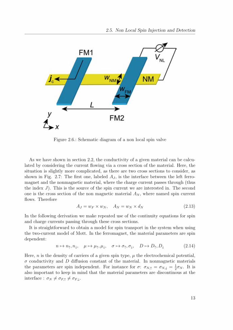
2.5.2. System
In order to obtain a general description of non local spin injection into nonmagneticmaterials, we consider the system shown in Fig. 2.6. It consists of two ferromagnetson top of a nonmagnetic material, forming two FM/NM junctions. The FMs havethe same width wF and height dF and the nonmagnetic material wN and dN . Thecenter-to-center distance of the FMs is labeled L. A bias current is applied to the lefthand FM/NM junction, so that a charge current flows only in the left hand part of thenonmagnetic material, while a voltage VNL is detected non locally between the NMand the second FM. This voltage is due to the spin accumulation close to the FM/NMinterface. The model system corresponds well to the experimental situation.
12
2.5. Non Local Spin Injection and Detection
Figure 2.6.: Schematic diagram of a non local spin valve
As we have shown in section 2.2, the conductivity of a given material can be calcu-lated by considering the current flowing via a cross section of the material. Here, thesituation is slightly more complicated, as there are two cross sections to consider, asshown in Fig. 2.7: The first one, labeled AJ , is the interface between the left ferro-magnet and the nonmagnetic material, where the charge current passes through (thusthe index J). This is the source of the spin current we are interested in. The secondone is the cross section of the non magnetic material AN , where named spin currentflows. Therefore
AJ = wF × wN , AN = wN × dN (2.13)
In the following derivation we make repeated use of the continuity equations for spinand charge currents passing through these cross sections.
It is straightforward to obtain a model for spin transport in the system when usingthe two-current model of Mott. In the ferromagnet, the material parameters are spindependent:
n 7→ n↑, n↓, µ 7→ µ↑, µ↓, σ 7→ σ↑, σ↓, D 7→ D↑, D↓ (2.14)
Here, n is the density of carriers of a given spin type, µ the electrochemical potential,σ conductivity and D diffusion constant of the material. In nonmagnetic materialsthe parameters are spin independent. For instance for σ: σN,↑ = σN,↓ = 1
2σN . It is
also important to keep in mind that the material parameters are discontinous at theinterface : σN 6= σF,↑ 6= σF,↓.
13

2. Theoretical Background
Figure 2.7.: Sketch of the current flow from Ferromagnet to non magnetic metal (viaAJ) and through it (via AN)
2.5.3. Derivation of the Diffusion Equation
In the following, we derive an expression for the non local voltage detected at the rightside of our system. First, we write down the continuity equations for spin and charge,which have to be conserved in the process. These equations read:
∇~jc = ∇(~j↑ +~j↓) = 0 (2.15)
∇~js = ∇(~j↑ −~j↓) = −eδn↑/τ↑↓ + eδn↓/τ↓↑ (2.16)
Equation 2.15 is the continuity equation for charge ∇~jc + ρc = 0, where we alreadydemanded a steady state situation: ρ = 0. In equation 2.16, δn↑,↓ is the deviationfrom equilibrium of carrier densities n↑,↓, while τ↑↓ (τ↓↑) is the characteristic time forspin flips from state ↑ (↓) to ↓ (↑). Therefore, eq. 2.16 accounts for the change incarrier density ni due to spin flips. We demand detailed balancing [42] between theseevents, meaning that
n↑τ↑↓
=n↓τ↓↑
(2.17)
The current densitity in the nonmagnetic material ~j↑,↓ can be written within thetwo current model as [41]
~j↑,↓ = −σ↑,↓∇V − eD∇δn↑,↓ (2.18)
Here, the first term is the spin dependent equivalent to eq. 2.1, while the second oneaccounts for diffusion of spins due to the deviation δn↑,↓ from equilibrium of the spin
14

2.5. Non Local Spin Injection and Detection
population. In a nonmagnetic material without external source of spin polarization,these populations are in equilibrium and eq. 2.18 becomes Ohm´s rule, eq. 2.1.Next, we use the Einstein relation between σ and n
σ↑,↓ = e2n↑,↓D (2.19)
and note that δn↑,↓ = n↑,↓δE↑,↓ [41]. It is therefore possible to use the energy E insteadof carrier density n as variable. We further define the electrochemical potential foreach spin sub band:
µ↑,↓ = E↑,↓ + eV (2.20)
where we use the bias voltage V . With these definitions, it is possible to write eq.2.18 as
~j↑,↓ = −(σ↑,↓/e)∇µ↑,↓ (2.21)
It follows for a spin current in nonmagnetic material
~js = −σNe∇µs (2.22)
This is the same result as Eq. 2.9.By using the continuity equations for charge and spin, Eq. 2.15 and 2.16, as well as
detailed balancing, eq. 2.17, in eq. 2.21, we obtain the spin diffusion equations [40]
∇2(σ↑µ↑ + σ↓µ↓) = 0 (2.23)
∇2(µ↑ − µ↓) = λ−2sf (µ↑ − µ↓) (2.24)
Equation 2.24 is equivalent to 2.10, as λsf =√Dτsf , where τ−1sf = 1
2(τ−1↑↓ + τ−1↓↑ ) and
D−1 = (n↑D−1↓ + n↓D
−1↑ )/(n↑ + n↓). Furthermore, here and in the following λsf = λN
and τsf = τN .
2.5.4. Interfacial Currents
In order to find solutions for µ↑ and µ↓ that satisfy eq. 2.23 and 2.24, one can writethe interfacial currents (for the interface at z = 0) as
I↑,↓i = (G↑,↓i /e)(µ↑,↓F |z=0 − µ↑,↓N |z=0) for i = 1, 2 (2.25)
where Gi is the interface conductance, Gi = G↑i + G↓i = R−1i . This allows us to takeinto account different regimes of the interface: In the transparent regime, Gi → ∞,the electrochemical potential are continous at the interface, while for the tunnelingregime, Gi is small. The interfacial charge and spin currents are given by Ici = I↑i + I↓iand Isi = I↑i − I
↓i .
15
2. Theoretical Background
In NM, the electrochemical potential only changes in the x direction (wN , dN λN).Therefore, µN can be written as
µ↑,↓N = µN ± δµN (2.26)
Here, the first terms describes the effect of the bias and the second one the spindependent shift of the electrochemical potential due to the ferromagnetic electrodes.The effect of the bias can be written as
µN =eI
σNx, x < 0 (2.27)
= 0, x > 0
which takes into account the layout of the system: The bias is applied only to the lefthand side ferromagnet. The second term of eq. 2.26 can be written as
δµN = a1e− |x|λsf + a2e
− |x−L|λsf (2.28)
for the spin injection at x = 0 by FM1 as well as a feedback term at x = L due toFM2. The spin current ~js flows from left to right according to eq. 2.21. This means
~js = −(σNe
)∇δµN
⇒ ~js = (σNeλsf
)(δµN)
The continuity of the spin current at each junction yields
ISi = 2σNANeλN
ai (2.29)
Using similar consideration, an expression for the interfacial currents in the FMscan be derived as well.
2.5.5. Spin Dependent Voltage
In order to give an expression for the spin dependent, nonlocal voltage detected atFM2, we introduce the following abbreviations: The spin resistances of NM and theFM are given by RN = ρNλN/AN respectively RF = ρFλF/AF . The interfacial current
polarization is given by PJ =∣∣∣G↑i −G↓i ∣∣∣ /Gi. Finally, the resistivities are ρN = σ−1N
and ρF = σ−1F .
16
2.5. Non Local Spin Injection and Detection
Using these definitions, the nonlocal voltage V2 detected at FM2 divided by theinjected current at FM1 can be written as [41]
V2/I = ±2RNe−L/λN
2∏i=1
(PJ
RiRN
1−P 2J
+pF
RFRN
1−p2F
)2∏i=1
(1 +
2RiRN
1−P 2J
+2RFRN
1−p2F
)− e−2l/λN
(2.30)
The + and - signs correspond to parallel and antiparallel alignment of the magnetiza-tions of FM1 and FM2. Experimentally, the detected voltage change due to the spinaccumulation is
∆VNL = 2|V2| = V P2 − V AP
2 (2.31)
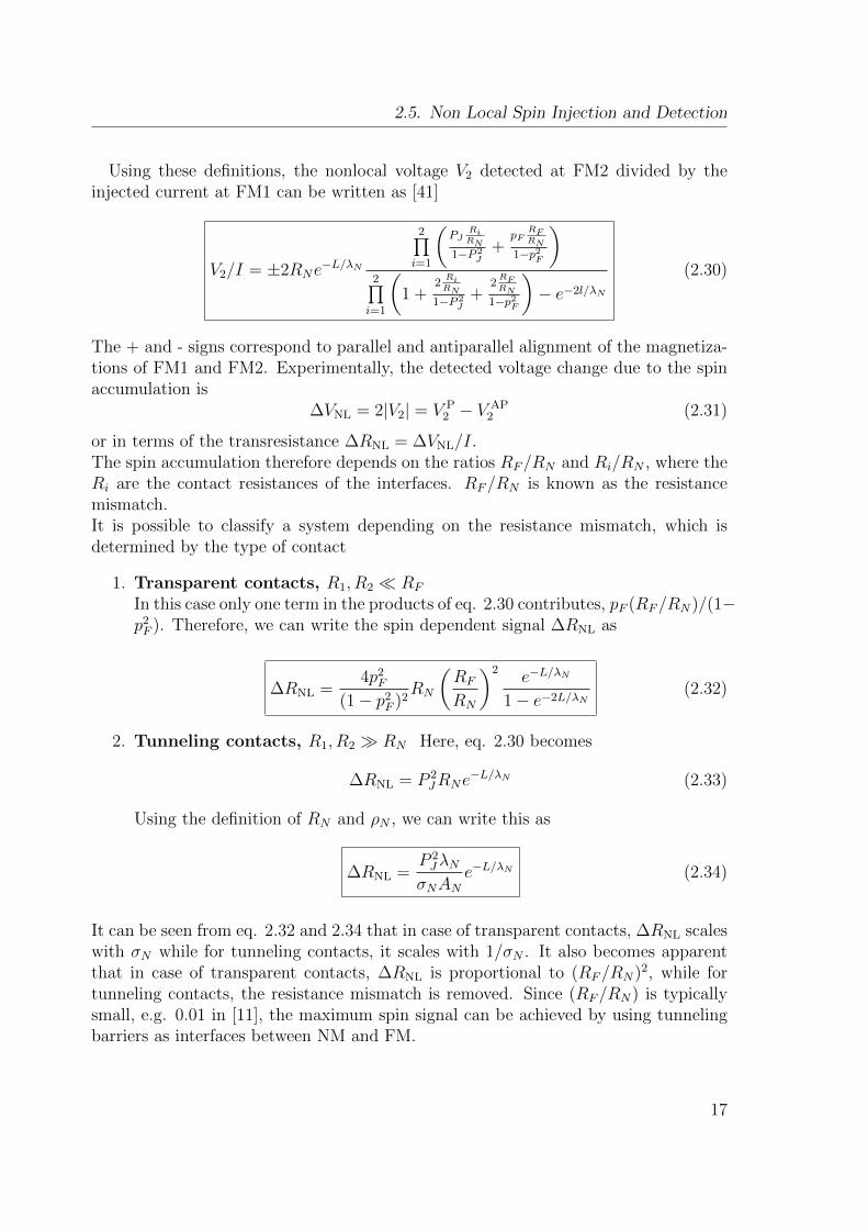
or in terms of the transresistance ∆RNL = ∆VNL/I.The spin accumulation therefore depends on the ratios RF/RN and Ri/RN , where theRi are the contact resistances of the interfaces. RF/RN is known as the resistancemismatch.It is possible to classify a system depending on the resistance mismatch, which isdetermined by the type of contact
1. Transparent contacts, R1, R2 RF
In this case only one term in the products of eq. 2.30 contributes, pF (RF/RN)/(1−p2F ). Therefore, we can write the spin dependent signal ∆RNL as
∆RNL =4p2F
(1− p2F )2RN
(RF
RN
)2e−L/λN
1− e−2L/λN(2.32)
2. Tunneling contacts, R1, R2 RN Here, eq. 2.30 becomes
∆RNL = P 2JRNe
−L/λN (2.33)
Using the definition of RN and ρN , we can write this as
∆RNL =P 2JλN
σNANe−L/λN (2.34)
It can be seen from eq. 2.32 and 2.34 that in case of transparent contacts, ∆RNL scaleswith σN while for tunneling contacts, it scales with 1/σN . It also becomes apparentthat in case of transparent contacts, ∆RNL is proportional to (RF/RN)2, while fortunneling contacts, the resistance mismatch is removed. Since (RF/RN) is typicallysmall, e.g. 0.01 in [11], the maximum spin signal can be achieved by using tunnelingbarriers as interfaces between NM and FM.
17

2. Theoretical Background
Figure 2.8.: Schematic representation of a non local spin valve measurement
In Fig. 2.8, we show a schematical representation of a non local spin valve mea-surement. At first we consider the black trace in Fig. 2.8: Starting at high negativemagnetic fields both FMs point up (↑↑), in direction of the field. This alignment doesnot change for negative magnetic fields. After crossing zero, the magnetic field pointsinto the direction opposite of the magnetizations of the FMs. The ferromagnetic elec-trode with the lower coercive field switches first, creating an anti parallel alignmentof the FMs (↑↓). The value of the non local voltage VNL switches as well. For idealdevices, the values of VNL for P and AP alignment are symmetric around zero and themagnitude ∆VNL is given by eq. 2.31. Further increasing the external field leads tothe switching of the second FM, creating P alignment again, but opposite in respectto the start of the measurement (↓↓).
Sweeping the field back in the opposite direction, a measurement of VNL results ina curve such as the red one in Fig. 2.8, which exhibits the same physics for oppositemagnetic fields, due to the hysteresis of the FMs.
2.6. Hanle Spin Precession
In section 2.5, we consider a system where the external magnetic field lies in the planeof the ferromagnetic electrodes of the spin valve devices. The non local voltage wedetect in these systems depends on the relative alignments of the magnetizations ofthe FMs. But what happens to this voltage when the magnetic field is tilted out ofplane, perpendicular to the magnetization of the ferromagnets, as shown in Fig. 2.9(a)?
In the following, we show that this results in a precession of the injected spins aroundthe external field. This is the Hanle effect, which originally described a magneticresonance phenomenom in gases [43].
We consider a system with tunneling contacts, meaning that Eq. 2.34 is valid. In
18

2.6. Hanle Spin Precession
combination with the Einstein relation, Eq. 2.19, we can write the voltage V2 detectedat FM2 as
V2 =1
2IP 2λNσNAN
e(−L/λN )
=1
2IP 2λNe2NDA
e(−L/λN ) (2.35)
where λN = λsf of the non magnetic material.Now, the perpendicular field induces a coherent precession of the spins injected by
FM1 with the Larmor frequency, which is determined by the external magnetic field:
Ω = γB⊥ =gµB
~B⊥ (2.36)
Here, g is the electronic g-factor, µB is the Bohr magneton and ~ is the reducedPlanck´s constant. At FM2, only the component parallel to the magnetization resultsin a measurable voltage, i.e. the projection of the magnetization of the spins to theaxis of FM2. The detected voltage V2 is therefore proportional to cos(Ωt).
Figure 2.9.: Hanle spin precession (a) NLSV in a perpendicular magnetic field. Themagnetization of the FMs can be P or AP, as indicated by the whitearrows. Spins injected into the NM precess around the external field (b)Normalized non local voltage as a function of the perpendicular field asgiven by Eq. 2.39
Furthermore, the diffusive nature of the electronic conduction has an effect on thedetected voltage as well. There are many possible paths with different lengths forthe diffusion of the electrons, which leads to a distribution in diffusion times. Thiscorresponds to a distribution in precession angles Ωt at FM2 given by [44]
f(t) =1√
4πDte(−L
2/4Dt) (2.37)
19

2. Theoretical Background
Additionally, we have to take into account the possibility of spin flips during thediffusion time t, which decays exponentially with τsf .
As these three contributions depend on t, one has to integrate over all possible timesin order to get the total contribution of the precession to the spin dependent voltage[42]
V2(B⊥) = ±I P 2
e2NAN
∫ ∞0
dt cos(Ωt)f(t)e(−t/τsf) (2.38)
Finally, for large perpendicular magnetic fields B⊥, the magnetization of the ferro-magnetic electrodes tilts out of the plane of the substrate with an angle θ. This effecthas to be included in the calculation of the spin dependent voltage [44]:
V2(B⊥, θ) = V2(B⊥) cos2(θ) + |V2(B⊥ = 0)| sin2(θ) (2.39)
An example is shown in Fig. 2.9 (b). By fitting the experimental data to Eq. 2.39, itis possible to extract values for λsf , τsf , D and therefore also P .
2.7. Spin Caloritronics
In section 2.2, we introduce charge and heat current as well as the Seebeck effect asan example for the interplay between the two. Together with the Peltier effect [34],which is the opposite of the Seebeck effect, these phenomena can be combined in thethermoelectric equations.
The newly emerging field of Spin Caloritronics deals with spin dependent versionsof these thermoelectric effects, such as the spin Seebeck effect (SSE) [23], or the spin-dependent Seebeck effect [45]. Our own group has contributed to the field with theexperimental realization of a magnon-drag thermopile [25].
In this theoretical introduction, our aim is to demonstrate how charge, heat andalso spin current are closely connected to each other. Further details regarding exper-imental advances can be found in chapter 7.
In respect to section 2.2, we introduce additional indices in Eq. 2.1 and 2.2: ~j0c =−σ∇V and ~j0h = −κ∇T Using these definitions, we can write the charge currentdensity in a given material as
~jc = σ(−∇V ) + σ(−S∇T ) (2.40)
Here, the first term on the right hand side is given by Ohm´s rule (~j0c ) and the secondone by the Seebeck effect. Charge transport in a metal is due to a gradient in electricalpotential or to a temperature gradient in the metal: ~jc = ~j0c +~jSeebeckThe heat current density can be written as
~jq = Π(−σ∇V ) + (−κ∇T ) (2.41)
20

2.7. Spin Caloritronics
where Π is the Peltier coefficient of the material. The first term on the right handside is given by the Peltier effect while the second one is Fourier´s rule. Similar toelectrical conduction, heat transport in a metal is caused by gradient in temperatureor electrical potential: ~jq = ~jPeltier +~j0qIt is therefore possible to write charge and heat current as components of a vector andthe coefficients as elements of a matrix, which operates on the gradients:(
~jc~jq
)= −σ
(1 SΠ κ/σ
)(∇V∇T
)(2.42)
The relation between spin and charge currents can be combined in the thermoelectricequations. By applying the two-current model introduced in section 2.3.1, the spindegree of freedom can be introduced into the theory in a similar way as in section 2.5.
Recall that the current densities for majority and minority spin are given by ~j↑ and~j↓, so that ~jc = ~j↑+~j↓ and ~js = ~j↑−~j↓. Also, as shown in section 2.5, ~js = −(σ/e)∇µs,where µs = µ↑ − µ↓. Finally, we define µc = (µ↑ + µ↓)/2, where µ↑,↓ = E↑,↓ + eV .
As pointed out in section 2.5, the simple equations for charge, heat and spin currentare formally equal. In each case, the current is a (linear) response to the generalizedforces, which are the gradients. It is possible to express this result in an elegant wayby defining a current vector [46]
~J = (~jc,~js,~jq) (2.43)
as well as a vector containing the generalized forces
∇X = (∇µc/e,∇µs/e,∇T ) (2.44)
Charge, spin and heat current can therefore be written as
~J = L∇X (2.45)
Here, L is a linear 3× 3-matrix, whose elements can be obtained by demanding thatEq. 2.45 fulfills Ohm´s rule (Eq. 2.1), Fourier´s rule of heat conduction (Eq. 2.2),Eq. 2.9 for the spin current, as well as the Seebeck effect (Eq. 2.3) and its inverse, thePeltier effect. The latter two are connected via an Onsager relation, Π = TS. Thisallows for eliminating off diagonal elements of the matrix, while the simple equationsfor spin, heat and charge current determine the diagonal elements. One obtains [24] ~jc
~js~jq
= −σ
1 P STP 1 P ′STST P ′ST L0T
2
∇µc/e∇µs/e∇T/T
(2.46)
where P and P ′ are the spin polarizations of the conductivity and the differentialpolarization at the Fermi energy:
P =σ↑ − σ↓σ↑ + σ↓
|EF, P ′ =
∂Eσ↑ − ∂Eσ↓∂Eσ↑ + ∂Eσ↓
|EF(2.47)
21

2. Theoretical Background
Equation 2.46 requires the Wiedemann-Franz-law to hold in order to be valid, so thatL0T = κ/σ, where L0 is the Lorentz number. In case of a nonmagnetic material,P = P ′ = ∇µs = 0 and Eq. 2.46 becomes Eq. 2.42. Finally, note that in the abovediscussion the charge current is understood as a sum of two independent spin channels,while this is not the case for the heat current. In principle the heat current has to betreated as a sum of spin up and down contributions as well, ~jq = ~j↑q +~j↓q . Consequently
a spin heat current ~jsq = ~j↑q − ~j↓q can be expected. The absence of such a spin heatcurrent can be justified by the assumption that there is no spin temperature gradientTs = T ↑ − T ↓ [47].
22

2.8. Graphene
2.8. Graphene
2.8.1. Introduction
Throughout the following section, we introduce basic properties of graphene, such asthe relativistic dispersion relation of the electrons and the electric field effect. Sincethe first succesful experimental observation of graphene in 2004 [18], these propertieshave been discussed multiple times. An excellent review can be found in [20]. However,since they are vital to the understanding of the work presented in the later chapters ofthis thesis, we shortly resume them here, before we discuss the topic of spin injectionand detection in graphene in section 2.9.
2.8.2. Band Structure of Graphene in the Tight Binding Approach
Graphene is a two dimensional structure consisting of carbon. The atomic structureof carbon allows for several types of bonding, which results in many different atomicconfigurations. One example is amorphous carbon, another one diamond. Graphite isanother example. Here, sp2 hybridization of the carbon atomic orbitals leads to strongbonds in a two-dimensional plane (we choose the xy plane, without loss of generality).In the third spatial direction, the atoms are coupled by van der Waals forces, resultingin much weaker bonds. Graphite can therefore be seen as a stack of twodimensionallayers only weakly coupled in the third dimension. These twodimensional layers aregraphene. Due to the interest in the properties of graphite, graphene has been studiedtheoretically from as early as 1947 [17].
The Brillouin zone (BZ) of graphene exhibits two points of special interest, the so-
called Dirac points ( ~K, ~K ′) at the corners of the first BZ. Around these points, E(~k)can be written as [20]
E±(q) = ±vF|q|+O[(q/K)2
](2.48)
Here, ~k = ~K + ~q, where |~q| ∣∣∣ ~K∣∣∣. The Fermi velocity vF is of the order vF ≈
1× 10⁶ m/s.
The dispersion relation E(~k) is shown in Fig. 2.10 (a) as a function of k. As a
function of kx, ky, E(~k) becomes a cone, as shown in Fig. 2.10 (b). These are theso-called Dirac cones. As in the case of semiconductors, the conduction in the upperband is mediated by electrons, while for the lower bands, the charge carriers are holes.
Equation 2.48 is a linear dispersion relation between energy and momentum, E ∝ q.This is similar to the particles described by the Dirac equation, which combines quan-tum mechanics and special relativity. In fact, around the Dirac points the chargecarriers can be described by an equation formally equivalent to the Dirac equation,only exchanging the speed of light by vF. Therefore, the conduction electrons ingraphene can be seen as relativistic particles.
23

2. Theoretical Background
Figure 2.10.: Dispersion relation of graphene close to the Dirac points (a) in one di-mension in k space (b) in two dimensions in k-space, forming the so-calledDirac cone
In the following, we show how these properties of the band structure of graphenecan be derived in an elementary way from its crystal lattice. The calculation is basedon the tight-binding method, which is a method to calculate the bandstructure of agiven materials based on a linear combination of its atomic orbitals [29]. Tight-bindingcalculations take into account that some of these orbitals might form non-negligibleoverlaps by introducing correction terms to the simple atomic picture.
The crystal structure of graphene is a hexagonal honeycomb as shown in Fig. 2.11.It can be understood as a triangular lattice, where the unit cell consists of two atoms.The lattice vectors are given by [17]
~a1 =a
2(3,√
3), ~a2 =a
2(3,−
√3) (2.49)
where a = 1.42 A is the lattice constant.It is also possible to understand the crystal structure of graphene as the superposi-
tion of two identical sublattices A and B, as indicated in Fig. 2.11.In order to understand electronic transport in graphene, we consider an electron
siting at site ~Ri on sublattice A. There are three nearest neighbors in the vicinity of~Ri in a distance a, and six second nearest neighbors. It becomes clear that the nearestneighbors belong to sublattice B and the second nearest neighbors to sublattice A.Disregarding higher order contributions, we can therefore describe the proces via acreator/annihilator algebra for both sublattices.
Be ai,σ an operator which annihilates an electron with spin σ =↑, ↓ on site ~Ri of
sublattice A, and a∗i,σ an operator which creates an electron with spin σ on site ~Ri.
24

2.8. Graphene
Figure 2.11.: The crystal structure of graphene forms a hexagonal honeycomb patternwith lattice constant a and lattice vectors a1 and a2. The structurecan also be seen as a triangular lattice with two atoms in per unit cell,resulting in sublattices A and B.
We define bi,σ and b∗i,σ in an analog fashion for sublattice B. Using these definitions,the tight-binding Hamiltonian for hopping of electrons between nearest and secondnearest neighbors takes the following form [20]
H = −t∑〈i,j〉,σ
(a†σ,ibσ,j + aσ,ib†σ,j)︸ ︷︷ ︸
hopping nearest neighbors
− t′∑〈i,j〉,σ
(a†σ,iaσ,j + b∗σ,ibσ,j + H.c.)︸ ︷︷ ︸hopping 2nd nearest neighbors
(2.50)
where we set ~ = 1 and H.c. is the Hermitian conjugate. The first term standsfor the hopping of electrons to the nearest neighbors, while the second one accountsfor the hopping to the second nearest neighbors. The parameters t and t′ are therelated hopping energies. Here, t ≈ 2.8 eV [20], while t′ has recently been determinedexperimentally to t′ ≈ 0.3 eV [48].
The energy bands derived from the tight-binding Hamiltonian read [17]
E± =± t√
3 + f(~k)− t′f(~k), where
f(~k) =2 cos(√
3kya) + 4 cos
(√3
2kya
)cos
(3
2kxa
)(2.51)
Here, the + sign refers to the upper and the - sign to the lower band. Now, we canobtain Eq. 2.48 by expanding the dispersion relation 2.51 around the Dirac points.
25

2. Theoretical Background
Figure 2.12.: Field effect in graphene for different substrates (a) Graphene sheet and p+
Si can be seen as two plates of a two dimensional capacitor (b) Grapheneon top of serveral dielectrica, the insulating layers can be seen as capac-itors in series. (c) Suspended graphene: Here, the second dielectric isvacuum
2.8.3. The Electric Field Effect
Carrier Density
The electric field effect of graphene means that the charge carrier concentration ofgraphene can be tuned by applying an external field [18]. It is thus a tool to changeproperties such as conductivity and resistivity. Here, we show how the strenght of theelectric field close to the graphene depends on the thickness and dielectric constant onwhich graphene is deposited.
We consider the following cases, as shown in Fig. 2.12, the field effect for one ormultiple dielectrica in series.
1. The electric field effect for one dielectric (Figure 2.12) (a)The graphene flake can be seen as one plate of a two dimensional capacitor. Thep doped Si substrate serves as the second electrode, while the two are separatedby the dielectric material SiO2. For a capacitor it is valid [49] that C = Q/U ,where Q = N ·e is the charge of the graphene flake and U = VBG is the backgatevoltage applied to the Si substrate. The capacitance C of a two dimensionalcapacitor is given by CDiel = (ε0εr/d)A, where ε0 is the dielectric constant, εrthe relative dielectric constant of the SiO2, d the distance between the plates(the thickness of the SiO2) and A the area of the flake. Using n = N/A, weobtain for the carrier concentration of the graphene [18]
n =ε0 εrd e
VBG (2.52)
The carrier concentration depends linearly on the backgate voltage, and fora voltage VBG = 0 it follows that n = 0. Here, we assume that the Diracpoint VD lies at zero backgate voltage. In experimentally fabricated graphene,
26

2.8. Graphene
a shift is observed frequently and in the above formulas we have to substituteVBG 7→ VBG − VD.
2. Multiple dielectrica in series (Figure 2.12 (b), (c))For the graphene devices, as shown in chapter 3.4.4 and 3.4.5, we have to extendthe above formula in order to use it for different substrates. In both cases,an additional dielectric layer separates the p doped Si and the graphene. Wecan therefore see these systems, as shown in Fig. 2.12, as two capacitors inseries. The total capacitance of such a system is given by [49] 1/C =
∑i 1/Ci.
Therefore, Eq. 2.52 becomes
n =ε1 ε0
e(d1 + d2ε1ε2
)VBG (2.53)
In summary, in both cases the carrier density can be expresed as
n = αVBG (2.54)
As shown, the parameter α depends on the geometry as well as on the material prop-erties of the system.
Gate Capacity
The capacity Cg between gate and substrate is closely related to the factor α. Thecharge carrier concentration of a 2D capacitor is given by n · e = Cg · VBG. Sincen = αVBG it immediately follows that
Cg = e · α (2.55)
For instance, in case of non suspended samples, that means that
Cg =ε0εrd
(2.56)
For our devices, we obtain
Dielectrica α [109V−1cm−2] Cg [ aFµm2 ]
440 nm SiO2 49 78,5285 nm SiO2 / 200 nm PMMA 44,5 71,2285 nm SiO2 / 200 nm vacuum 20 32
27

2. Theoretical Background
Seebeck coefficient
As noted in section 2.2, the Mott relation of the Seebeck coefficent reads
S = −π2k2BT
3|e|1
σ
∂σ
∂Vg
∂Vg∂E|E=EF
(2.57)
where
∂Vg∂EF
=
√|e|Cgπ
2
~vF
√|∆Vg| (2.58)
with the Fermi velocity vF and ∆Vg = Vg − VD. Therefore, S can be written as
S = −π2k2B3|e|
√|e|Cgπ
2~vFT ·√|∆Vg| 1σ
∂σ∂Vg
= A ·√|∆Vg| 1σ
∂σ∂Vg
(2.59)
where A is a parameter depending on the geometry and on the temperature of thesample. For our different types of sample we obtain
Dielectrica A at RT A at 77 K A at 4.2 K
440 nm SiO2 564 ·10−6 145 ·10−6 7.9 ·10−6
285 nm SiO2 / 200 nm PMMA 578 ·10−6 149 ·10−6 8.1 ·10−6
285 nm SiO2 / 200 nm vacuum 1111 ·10−6 285 ·10−6 15.6 ·10−6
Finally, the latter three expressions in eq. 2.59 can be obtained by measuring σ(VBG)and numerically processing the data.
Residual Carrier Concentration
The carrier concentrations given by eq. 2.54 are calculated taking into account only theeffect of the electric field and the nature of the graphene crystal. However, extrinsicsources such as impurities, adatoms or ripples in the graphene also contribute tothe carrier concentration. This can be accounted for by expressing the total carrierconcentration as [50]
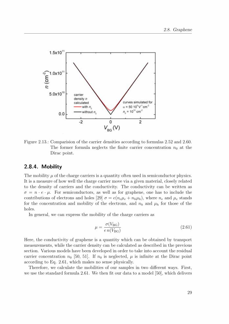
ntot =√n20 + n(VBG)2 (2.60)
For our devices, the residual carrier concentration is of the order of n0 = 1011 cm−2,meaning that it can be mostly neglected. However, close to the Dirac point, theresidual carrier concentration matters, as we show graphically in Fig. 2.13 Especially,when extracting the mobilities of the devices, it is important to take into account theextrinsic carrier concentration at the Dirac point as we show in the following section.
28
2.8. Graphene
Figure 2.13.: Comparision of the carrier densities according to formulas 2.52 and 2.60.The former formula neglects the finite carrier concentration n0 at theDirac point.
2.8.4. Mobility
The mobility µ of the charge carriers is a quantity often used in semiconductor physics.It is a measure of how well the charge carrier move via a given material, closely relatedto the density of carriers and the conductivity. The conductivity can be written asσ = n · e · µ. For semiconductors, as well as for graphene, one has to include thecontributions of electrons and holes [29] σ = e(neµe + nhµh), where ne and µe standsfor the concentration and mobility of the electrons, and nh and µh for those of theholes.
In general, we can express the mobility of the charge carriers as
µ =σ(VBG)
e n(VBG)(2.61)
Here, the conductivity of graphene is a quantity which can be obtained by transportmeasurements, while the carrier density can be calculated as described in the previoussection. Various models have been developed in order to take into account the residualcarrier concentration n0 [50, 51]. If n0 is neglected, µ is infinite at the Dirac pointaccording to Eq. 2.61, which makes no sense physically.
Therefore, we calculate the mobilities of our samples in two different ways. First,we use the standard formula 2.61. We then fit our data to a model [50], which delivers
29

2. Theoretical Background
the residual carrier concentration n0. Obviously, we have to disregard all values belown0, as demonstrated graphically in Fig. 5.2.The model used for the fitting accounts for the effect of the finite intrinsic carrierconcentration as well as the contact resistance RC [50]. The mobility is a constantfitting parameter within the model and the total resistance Rtot of a device measuredin 4 point configuration is given by
Rtot = RC +1
eµ√n20 + n(VBG)2
(2.62)
The constant mobilities extracted by the fitting correspond well with the values ex-tracted by the standard formula close to n0.
2.9. Spin Relaxation in Graphene
2.9.1. Introduction
The phenomenological model of spin injection and detection in metals, as describedin section 2.5, is applicable to graphene with only minor modifications. These ba-sically consist of substituting three-dimensional quantities by their two-dimensionalcounterparts. For example, the cross section of the non magnetic material AN is sub-stituted by the width W of the graphene flake in Eq. 2.34. The equation then reads∆RNL = ((P 2
JλN)/(σNW )) exp(−l/λN)). Here, the quantity σN is the two-dimensionalconductivity of graphene and unlike for metals, σN = σN(VBG). However, apart fromthese modifications, we can apply the model of spin injection and detection in nonmagnetic materials as developed in section 2.5.
Here, we instead focus on the features of graphene that make it a promising candi-date for applications in spintronics.
To start with, graphene exhibits excellent electrical properties [20]. High mobilitiesand the ability to tune the charge carrier concentration allow for studies which are notpossible in metals, where the carrier concentration can not be varied by an externalgate. The fact that the conduction electrons behave as relativistic particles makesgraphene an even more interesting physical system. Moreover, the band structure ofgraphene can be tuned by the introduction of adatams [52]. Finally, as a gapless semi-conductor, graphene allows for fascinating experiments combining spin and charge, aswe show in chapter 7.
In the context of spintronics, it is important to note that Carbon is a relatively lightmaterial (Z = 6) and the spin-orbit interaction is low. The most frequent isotope, 12C,has no nuclear spin an thus no hyperfine interaction. Therefore, long spin relaxationlengths of several µm can be expected. This is longer than in most metals, where λsfis of the order of tens or hundreds of nm [53]. In fact, first successful experiments
30

2.9. Spin Relaxation in Graphene
Figure 2.14.: Schematic representation of Elliot Yafet spin relaxation
on spin injection in graphene have demonstrated λsf of the order of a few microns[54, 55, 56, 57]. These experiments have been carried out in relatively dirty systemswith low mobilities or in multilayer graphene. Fueled by the experimental results,theorist have predicted λsf of the order of tens or hundreds of µm in clean, highmobility systems [58, 59]. These predictions are based on extrapolations of the Elliot-Yafet (EY) as well as by the D‘yakonov-Perel (DP) spin relaxation mechanism, whichwe introduce in the following.
2.9.2. Elliot-Yafet Spin Relaxation
The EY mechanism is schematically shown in Fig. 2.14. A conduction electron getsscattered several times while passing through a given material. There is a finite prob-ability of a spin flip during scattering events, so the electron eventually changes itsspin orientation.
EY spin relaxation is often the dominant spin relaxation mechanism in metals, asthis type of relaxation appears in systems where spin orbit coupling is present togetherwith an inversion symmetry of the crystal lattice.
The presence of the spin orbit interaction has an effect on the Bloch states of thematerial, which become linear combinations of up and down states, |↑〉 and |↓〉. If thesystem exhibits inversion symmetry, they can be written as [60]
ψ~kn↑(~r) = [a~kn(~r) |↑〉+ b~kn(~r) |↓〉]ei~k·~r
ψ~kn↓(~r) = [a∗−~kn(~r) |↓〉+ b∗−~kn(~r) |↑〉]ei~k·~r (2.63)
where a and b are lattice vectors, given by the periodicity of the crystal. For |a| = 1and |b| = 0, these wavefunctions become simply |↑〉 and |↓〉, while for |a|, |b| 6= 0, thespin up and down states mix. In most cases however, |a| is close to one and |b| 1
31
2. Theoretical Background
[15]. Pertubation theory delivers |b| ≈ ∆so/∆E 1, where ∆E is the difference inenergy between a given state in one energy band and the nearest state in another bandwith the same momentum, and ∆so is the SO coupling between these two states.
At high temperature, elastic scattering is mainly caused by phonons, while at lowtemperature, scattering with impurities is the dominant cause. Direct coupling ofphonons with the spin up and down states have been studied and introduced to themodel by Yafet [61].The Elliot relation contains the scattering time τe, the spin flip time τsf and relatesthose to the shift of the electronic g-factor τe/τsf ≈ (∆g)2. In the Born approximation,this can be estimated to
τe/τsf ≈⟨b2⟩
= (∆so/∆E)2 (2.64)
Therefore, if the EY spin relaxation mechanism is the dominant one in a given mate-rial, the mean free time τe is proportional to the spin flip time τsf , τel ∝ τsf . It becomesclear that τsf depends inversely on the strength of the spin orbit interaction.
In graphene, the SO interaction close to the Dirac point can be expressed as [58]
∆so = ∆curv + ∆ext (2.65)
Here, ∆curv is the SO interaction due to curvature of the graphene sheet and ∆ext thecontribution due to external fields. The spins precess around the effective SO fieldwith the the spin precession length lprec = 2πvF/∆so [59].
As the electrons traverse graphene, they weakly scatter off the ions. During thesescattering events a certain amount of spin relaxes given by [59] ∆so/vFkF. After Ncollisions, the amount equals
√N∆so/vFkF. Dephasing occurs when
√N∆so/vFkF =
2π.Since τsf = N · τe, we obtain
τEYsf = τe4π2v2Fk
2F
∆2so
(2.66)
and
λEYsf ∼ λevFkF∆so
(2.67)
The last relation follows from the fact that λsf =√D · τsf and D = v2Fτ/2.
2.9.3. D‘yakonov-Perel Spin Relaxation
D´yakonov and Perel [62] have described a mechanism of spin relaxation in systemslacking inversion symmetry in their crystal lattice. There, states within the same bandof the same momentum ~k, but with opposite spins are not degenerate, E~k↑ 6= E~k↓.Therefore, these states are spin split. The effect on the spin orbit coupling can be
32

2.9. Spin Relaxation in Graphene
Figure 2.15.: Schematic representation of spin relaxation according to the D‘yakonov-Perel mechanism
described as an effective magnetic field ~B(~k) which depends in strength and direction
on the wavevector ~k of the electrons.
The DP mechanism is schematically shown in Fig. 2.15. The spins precess aroundB(~k). As the field depends on ~k, a distribution of electrons with different ~k would losea prepared spin orientation fast. However, typically there are many scattering eventschanging rapidly the momentum and effective magnetic field (to B(~k′) in the figure),before a spin can precess only once. This results in a supression of the spin relaxationand is called motional narrowing.
In graphene, the corresponding spin relaxation time can be expressed as [59]
τDPsf ≈
vFλe∆2
so
=1
τe∆2so
(2.68)
and
λDPsf =
vF√2∆so
(2.69)
Therefore, if the spin relaxation in graphene is dominated by the DP mechanism,then τsf ∝ τ−1e .
2.9.4. Comparison between EY and DP Mechanism
Both the EY as well as the DP mechanism are due to SO interaction. However, incase of the EY mechanism, the spin relaxation takes place during the scattering events,while for the DP mechanism, it happens in between these events.
In both cases τsf ∝ ∆−2so and λsf ∝ ∆−1so . Therefore, in systems with low spin orbitinteraction, the spin relaxation times and lengths are long. The smaller ∆so, the largerthe values of both τsf and λsf .
33
2. Theoretical Background
The relations 2.66 and 2.68 show how τsf scales with the elastic mean free path ofthe electrons. From the nature of the the two spin relaxation mechanisms however,one should expect that the EY mechanisms dominates in samples of low mobility andDP in samples of high mobility, as the time between scattering events increases forcleaner samples. The DP mechanism should hence constitute an upper limit for thespin relaxation time and length in graphene.
The relation between scattering time τe and spin flip time τsf is often used to dis-tinguish between relaxation mechanisms. If the origin of spin relaxation in a givenmaterial is given by the EY mechanism, it is valid that τe ∝ τsf , while for the DP mech-anism τe ∝ τ−1sf . This approach has been used to analyze a number of experiments ingraphene.
2.9.5. Experimental Results
Several experimental studies have found the EY relaxation mechanism to be the dom-inant one in graphene [63, 64, 65], but examples exist where the DP mechanism dom-inates the spin relaxation [66]. Moreover, Han et al. have found the spin relaxationat low temperatures to be dominated by EY in SLG, but by the DP mechanism inbilayer graphene (BLG) [67].
Recently, studies of spin injection in high mobility samples have become availableas well [68, 69]. Also here, λsf has been found to be of the order of a few µm. It istherefore obvious that the simple extrapolation based on the EY mechanism does nothold, leading to the conclusion that the initial theoretical predictions have overlookedlimiting factors for the spin relaxation in graphene.
These findings underline the need to further investigate the spin relaxation ingraphene, both theoretically and experimentally.
2.9.6. Further Mechanisms of Spin Relaxation in Graphene
Concluding the chapter, we discuss possible causes for spin relaxation in grapheneapart from the EY and the DP mechanism.
Imperfections in the graphene crystal lattice can be taken into account by introduc-ing a Gauge Field (GF) tensor A(~r), which is proportional to the strain tensor uij(~r).The GF leads to a pseudomagnetic field B⊥, which is perpendicular to the plane ofthe graphene, and thus perpendicular of the polarization of the injected spins as well.The presence of B⊥ leads to different spin relaxation times for spins in and out ofplane [59].
At the same time, it is an intriguing possibility to obtain high pseudomagnetic fieldsby choosing the right strain applied to the graphene sheet. This approach has becomeknown as strain engineering, and fields of tens of Tesla have been predicted by choosingthe appropriate strain tensor uij [70]. Experimentally, even higher pseudomagneticfields have been demonstrated in the vicinity of nanobubbles on top of graphene [71].
34

2.9. Spin Relaxation in Graphene
Recently, it has been proposed that the spin relaxation in graphene is due to anentanglement between spin and pseudospin mediated by spin orbit interaction [72].
Another possible reason for spin relaxation in graphene are impurities in the graphenecrystal or in the substrate. The substrate itself has been identified to affect the prop-erties of graphene. It is therefore desireable to eliminate the substrate by suspendingthe graphene spin valves [68]. Measurements of such systems can be found in chapter5.
35


3. Experimental Techniques andMethods
3.1. Introduction
Throughout this chapter, we describe the experimental techniques used for the fabri-cation of our nanoelectronic devices.
Firstly, in section 3.2, we describe the efforts we have taken in the context of thisthesis in order to obtain and characterize single layer graphene.
Secondly, in section 3.3, the results obtained concerning the fabrication of crosslinkedPMMA structures are summarized. The method presented here is is the first step inthe fabrication of our graphene devices.
In section 3.4, we discuss techniques needed for the device fabrication. This includeselectron-beam lithography as well as selection of the substrate for graphene exfoliation.Finally, we discuss the fabrication of freely suspended graphene spin valves.
As a concluding section, we discuss the experimental setup and basic electricalconnections used for the measurements on our devices.
3.2. Fabrication and Characterization of Single LayerGraphene
3.2.1. Mechanical Exfoliation
There are several techniques in order to obtain single layer graphene (SLG) flakes,which include chemical vapor deposition (CVD) [73], molecular beam epitaxy (MBE)[74] and synthesis on a Silicon carbide substrate [75]. Throughout this thesis, we haveexclusively used mechanically exfoliated graphene, as it is among the highest qualitygraphene in terms of mobility [19].
Mechanical exfoliation of graphene is commonly known as the Scotch tape method[18]. Since graphite consists of several layers of graphene only weakly bond to eachother by van der Waals interaction, intact graphene sheets can be obtained by peelingoff layers from the bulk. Hence, the quality of the graphite is a determining factor forthe quality of the graphene flakes [21], which makes it mandatory to use high qualitygraphite as bulk material.
37

3. Experimental Techniques and Methods
Figure 3.1.: Raman spectra of graphene: (a) Single layer graphene. (b) Bilayer andtriple layer graphene. Spectrum of BLG shifted for clarity. Insets: Opticalmicroscope images of the flakes. The scale bar equals 2µm.
The graphite flakes or nuggets are applied to a piece of wafer tape or common Scotchtape. Pressing a flake between two adhesive layers of tape and carefully separatingthe tapes again results in increasingly thin layers of graphite. At a certain point,these layers start to become transparent to light, indicating that the graphite consistsonly of a few layers of graphene. Pressing the tape on a substrate, e.g. Si/SiO2, itis likely that in some areas graphene flakes stick to the substrate when the tape isremoved. Once deposited on the substrate, the graphene can be further processed bynanolithography methods such as electron beam lithography (see section 3.4) or localanodic oxidation with an atomic force microscope (AFM) [76].
3.2.2. Optical Characterization and Raman Spectroscopy
Despite being atomically thin, graphene can be visualized by an optical microscope ifthe thickness of the SiO2 is appropriate [21, 77], due to an interference effect betweenthe light backscattered from the empty wafer and the flake. An optical microscopeimage of exfoliated graphite can be seen in the inset of Fig. 3.1 (a). The flake isexfoliated on a Si/SiO2 substrate, where the thickness of the SiO2 is 440 nm.
It is indeed possible to determine the number of graphene layers of a flake by care-fully examining its color and transparency. However, in order to verify that the de-termined number of layers in a given area is correct, it is necessary to quantify thenumber of layers of a reference sample beforehand. A fast and reliable method inorder to achieve that is by measuring Raman spectra [78], which requires to center themonochromatic light of a laser on the material under examination. Inelastic scatter-ing between between phonons with photons cause a shift in frequency of the photons,leading to a resonance spectrum of the scattered light characteristic for each material.
The Raman spectrum of SLG consists of a characteristic peak close to 2700 cm−1,
38

3.2. Fabrication and Characterization of Single Layer Graphene
Figure 3.2.: The 2D peak for (a) SLG (b) BLG (c) TLG
the 2D peak of graphene [79]. For multi layer graphene (MLG), a second peak appearsin the spectrum, the G peak at 1600 cm−1. Moreover, the shape of the 2D-peak servesas additional indication for the number of layers [79].
Raman spectra of SLG, bilayer graphene (BLG) and triple layer graphene (TLG)are shown in Fig. 3.1. These flakes are exfoliated on SiSiO2 substrates (440 nm oxidethickness), optical microscope images are shown in the inset of the figure. The flakeshown in Fig. 3.1 (b) consists of two areas of different thickness, where we haveperformed two independent Raman measurements.
It becomes clear that the spectrum shown in (a) is indeed a SLG Raman spectrum,as the G peak is not visible. It is also clear that the flake shown in Fig. 3.1 (b) is anexample of MLG, as the spectra, measured at the two different locations indicated bythe arrows, exhibit the G peak.
Figure 3.2 shows in detail 2D peaks of the same samples. In SLG, the 2D peakconsist of a single component, while for higher number of layers, the peak evolves intomultiple components. It is therefore possible to identify the Raman spectrum shownin Fig. 3.2 (b) as that of BLG, and the one in (c) as TLG.
Then, using the optical microscope images of these selected flakes as reference,one can thus reliably determine the number of layers of a graphene flake. We haverepeated the Raman measurements for each type of substrate used for this thesis,obtaining consistent results.
3.2.3. AFM characterization
Another method commonly used to charcterize graphene is atomic force microscopy. Itprovides deep information about height, impurities, ripples and edges of the grapheneflakes. Therefore, in order to ensure the highest possible quality of the graphene, oneshould perform AFM characterization measurements on flakes choosen for devices.
The working principle of an AFM is relatively straightforward [80]. An atomicallysmall tip, a so-called cantilever is moved across the surface of a sample, driven by a setof piezo crystals controlling the lateral movement. As the tip moves across the surface,
39
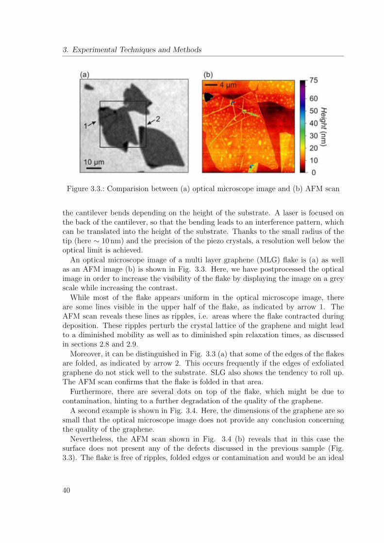
3. Experimental Techniques and Methods
Figure 3.3.: Comparision between (a) optical microscope image and (b) AFM scan
the cantilever bends depending on the height of the substrate. A laser is focused onthe back of the cantilever, so that the bending leads to an interference pattern, whichcan be translated into the height of the substrate. Thanks to the small radius of thetip (here ∼ 10 nm) and the precision of the piezo crystals, a resolution well below theoptical limit is achieved.
An optical microscope image of a multi layer graphene (MLG) flake is (a) as wellas an AFM image (b) is shown in Fig. 3.3. Here, we have postprocessed the opticalimage in order to increase the visibility of the flake by displaying the image on a greyscale while increasing the contrast.
While most of the flake appears uniform in the optical microscope image, thereare some lines visible in the upper half of the flake, as indicated by arrow 1. TheAFM scan reveals these lines as ripples, i.e. areas where the flake contracted duringdeposition. These ripples perturb the crystal lattice of the graphene and might leadto a diminished mobility as well as to diminished spin relaxation times, as discussedin sections 2.8 and 2.9.
Moreover, it can be distinguished in Fig. 3.3 (a) that some of the edges of the flakesare folded, as indicated by arrow 2. This occurs frequently if the edges of exfoliatedgraphene do not stick well to the substrate. SLG also shows the tendency to roll up.The AFM scan confirms that the flake is folded in that area.
Furthermore, there are several dots on top of the flake, which might be due tocontamination, hinting to a further degradation of the quality of the graphene.
A second example is shown in Fig. 3.4. Here, the dimensions of the graphene are sosmall that the optical microscope image does not provide any conclusion concerningthe quality of the graphene.
Nevertheless, the AFM scan shown in Fig. 3.4 (b) reveals that in this case thesurface does not present any of the defects discussed in the previous sample (Fig.3.3). The flake is free of ripples, folded edges or contamination and would be an ideal
40

3.3. Properties of Crosslinked PMMA
Figure 3.4.: Comparision between (a) optical microscope image and (b) AFM scan
candidate for further processing.
3.3. Properties of Crosslinked PMMA
3.3.1. Crosslinking PMMA
Throughout this thesis, we present spin injection measurements on graphene spinvalves on different substrates. We have fabricated freely suspended graphene spinvalves as well as spin valves on poly(methyl methacrylate) (PMMA) substrates. Bothtypes require the use of crosslinked PMMA, which we discuss in the following, whilethe complete fabrication process of each type of sample is given in section 3.4.
PMMA is one of the most common polymers used in the fabrication of nanodevices[81]. It is often used as positive resist in electron beam lithography, which we describein section 3.4. Here, we focus on the properties of crosslinked PMMA and present theresults of extensive tests. These test have been performed in order to use crosslinkedPMMA in combination with more established EBL techniques [82], as described insection 3.4.4 and 3.4.5.
PMMA can also be used as a negative resist by exposing the polymer to a doseapprox. 20 times higher than that required in the regular process. The overexposureresults in a crosslinking of the PMMA molecules, which perform a so-called glasstransition. Although the technique is well-known [83], considerable efforts have beentaken in the context of this thesis in order to apply it to the fabrication of freelysuspended graphene spin valves.
These efforts have been necessary for two reasons:
1. Reports in the literature on crosslinked PMMA in combination with conventionalEBL are rather scarce. If any, there are reports on using crosslinked PMMA as asubstrate for graphene [84], or as insulating layer in order to fabricate a topgateover an otherwise completed device [63, 85, 86, 87]. In these cases, it is sufficient
41

3. Experimental Techniques and Methods
to crosslink a rectangular area of dimensions considerably larger than the deviceitself.
However, in order to suspend graphene using crosslinked PMMA structures, ahigh precision of the process is required. In the following we demonstrate thatit is indeed possible to obtain a precision similar to that of the regular EBLprocesses and how to use crosslinking as a high definition tool. The completeprocess of suspending graphene spin valves is described in section 3.4.5.
2. We argue that the method to fabricate our samples has a beneficial effect ontheir spin injection properties, as we demonstrate in chapter 6. There, we ar-gue that the overexposure of the PMMA leads to the deposition of a layer ofamorphous carbon on top of the graphene sheets, which greatly enhances thespin injection due to a larger contact resistance between cobalt and graphene.It is thus important to gain insight into the detailed nature of our fabricationprocess.
We performed our preliminary tests as follows: Similar to a dose test in conventional
Figure 3.5.: Schematical representation of the fabrication process of crosslinkedPMMA structures (a) Overexposure of a layer of PMMA on top of aSi/SiO2-substrate by electron beam (b) Substrate after removal of theremaining PMMA
EBL [82], we overexpose an area of PMMA with a high dose of electron beam radiationfirst. (Fig. 3.5 (a)). As shown in Fig. 3.5 (b), this results in an area of crosslinkedPMMA, while the remaining polymer is removed in acetone. In order to investigatethe surface properties of the overexposed PMMA, we performed AFM scans on thetest samples. All structures shown here have been written at an acceleration voltageof 30 keV, using an aperture of 20µm. However, we have performed the same testsusing an aperture of 120µm, obtaining consistent results. Like in regular EBL, thediffererence between the two apertures is the sharpness of the edges of the definedstructures.
3.3.2. Choosing the Stepsize
An important property of the writing process by EBL is the stepsize of the scanningelectron microscope (SEM). While exposing the polymer, the electron beam (e-beam)
42

3.3. Properties of Crosslinked PMMA
moves across the surface of the substrate in discrete steps. The exposure takes placein square areas, whose sides correspond to the stepsize of the system: The e-beam ismoved to the first square, exposes the polymer with the specified dose, and is thenmoved to the next square. If the stepsize is too large, the crosslinking process doesnot result in an uniform surface, as shown in Fig. 3.6.
Figure 3.6.: AFM images of a preliminary test sample, consisting of a layer ofcrosslinked PMMA on top of a Si/SiO2-substrate as well as on top ofa metal substrate (a) The areas are (A) crosslinked PMMA on top ofmetal (B) metal surface without PMMA (C) crosslinked PMMA on topof Si/SiO2 substrate (D) Si/SiO2 substrate (b) AFM scan of the centralsquare of (a) Inset of (b): Height profile along the dashed line in (b) Theheight of the dots equals ∼45 nm, while in between, the height drops to∼30 nm
In the figure, we show an AFM scan of a test sample. The horizontal line in the imageseparates areas of a Si/SiO2 substrate (bottom)from the same substrate covered bymetal (top). Likewise, the vertical line separates areas covered by overexposed PMMA(left) as well as without it (right). It can be seen that the PMMA is sticking well onboth the Si and the metal substrate.
In Fig. 3.6 (b) we show a second AFM scan of the central cross section in (a). Thesurface of the crosslinked PMMA exhibits a periodic structure. It consists of dotsseparated by 100 nm, corresponding to the stepsize used during the EBL of this testsample. A larger amount of PMMA is thus crosslinked in the center of each writingfield. In the inset of Fig. 3.6 (b), we show the height profile of the AFM scan alongthe dashed line in the image. The height of the dots within the PMMA is approx.45 nm, while the valleys in between exhibit a height of 30 nm.
These results demonstrate that a small stepsize has to be chosen during the EBL inorder to obtain an uniform surface of the crosslinked PMMA. For the following workwe have used a stepsize of 15 nm, for which the roughness is no longer visible.
43

3. Experimental Techniques and Methods
3.3.3. Choosing the Electron Beam Dose
In order to determine the appropriate dose required to crosslink PMMA, one has tokeep in mind that on the one hand, the dose has to be as low as possible in order tominimize the exposure of the graphene flakes during the fabrication process. On theother hand, the dose has to be high enough in order to reliably crosslink the polymer.
Therefore, we have fabricated structures that consist of stripes of 2µm width ofgradually varying dose. It is convenient to discuss our results in terms of the dosefactor instead of the total dose (dose = area dose × dose factor). The area doseequals 300µC/cm2 for all structures shown, which is roughly the dose required toexpose PMMA as positive resist. Therefore, a dosefactor 30 means that we use 30times the dose needed for conventional EBL.
Figure 3.7.: (a) AFM scan of an area of two layers of crosslinked PMMA, with thedose factor varying in steps of five (b) Height profile along the x-axis (c)Thickness of the crosslinked polymer as a function of dose factor
In Fig. 3.7 (a), we show an AFM scan of such a structure. An averaged heightprofile along the x-axis is shown in (b).
The height of the profile as a function of dose factor is shown in (c). We can drawthe following conclusions from this analysis:
1. Height as function of dose The height profile as well as the height of thePMMA as a function of the dose factor (Fig. 3.7 (b) and (c)) indicate thatPMMA starts to crosslink at dose factor 15. For higher doses, the height startsto saturate to a value around 110 nm. This result is in good agreement with the
44

3.3. Properties of Crosslinked PMMA
nominal height of the PMMA before overexposure, which is approx. 120 nm [81]for the parameters used here (2 layers of PMMA 950 spincoated at 2500 rpm).
2. Reduced proximity effect The height of the crosslinked PMMA drops at adose factor of 50, as shown in Fig. 3.7 (b) and (c). This is due to the geometry ofthe structure. All areas receive a certain amount of radiation when the adjacentarea is exposed, however for the two outer areas (dose factor 5, not visible, and50), this effect is reduced, as there is only one adjacent area. The last data pointof (c) should hence be disregarded.
3. Structure of the surface A rectangular pattern can be distinguished in theAFM image shown in Fig. 3.7 (a). As opposed to the structure discussed insection 3.3.2, the pattern shown here is not due to the stepsize of the SEM, whichequals 10 nm for this test, while the pattern here repeats in steps of 0.67µm inthe x-direction.
The structure is most likely due to the internal processing of the area within thememory of the EBL system. However, the resulting differences in height of thepolymer are negligible and the surface is sufficiently even for our purposes.
Figure 3.8.: (a) AFM scan of an area of two layers of crosslinked PMMA, with thedose factor varying in steps of three (b) Height profile along the x-axis (c)Thickness of the crosslinked polymer as a function of dose factor
These conclusions are confirmed by several test samples. We show a second examplein Fig. 3.8. As before, we show an AFM image of the PMMA in Fig. 3.8 (a), a heightprofile in (b) and the height as a function of the dose factor in (c). In case of the
45

3. Experimental Techniques and Methods
sample presented here, we increase the dose factor in steps of three. Again, we findthat the PMMA starts to crosslink at dose factor 15. At dose factor 18, the PMMA iscompletely covering the surface of the chip, with a height of approx. 65 nm. At dosefactor 30, the height is approx. 100 nm and the surface of the polymer is sufficientlyuniform for our purposes.
Based on these results, we choose a dose factor 30 for crosslinking the PMMA,which corresponds to a total dose of 9000µC/cm2. We also exploit the dependence ofthe height of the PMMA in an way which is essential for the fabrication of our thinmetallic electrodes, as we show in section 3.3.5.
3.3.4. Creating trenches in overexposed PMMA
In order to suspend graphene using crosslinked PMMA, it is necessary to be able tocreate trenches within the crosslinked areas. Because of the high doses used duringthe exposure of the polymer, it is natural to assume that the proximity effect plays amajor role for the fabrication process, especially for narrow trenches of a few hundredsof nanometers in width. Again, we have fabricated several samples in order to verifythe feasibility of our method.
In Fig. 3.9, we show an AFM scan of such an structure. It consists of an area ofcrosslinked PMMA, where certain areas are not exposed to the e-beam. The width ofthe these trenches are 2/1/0.8/0.5µm. It becomes visible that these areas are free ofPMMA after lift-off in acetone.
The height profile, shown in Fig. 3.9 (b), confirms this observation. There areartefacts of the scan visible at the edges of the trenches. However, it is clearly visiblethat the PMMA is completely removed during lift-off and no polymer remains on thebottom of the trench.
We have found that for smaller widths of the trench, this is not always the case.The proximity effect is more pronunced for trenches smaller than 200 nm, when usingtwo layers of PMMA and for trenches smaller than 300 nm for four layers of PMMA.In these cases, few tens of nanometers remain at the bottom of the trench after lift-off.We can conclude that the proximity effect is more pronounced for multiple layers ofPMMA. For less numbers of layers, narrower trenches can be defined.
3.3.5. Controlling the Height Profile of the Polymer Substrate
As demonstrated in section 3.3.3, the height of the crosslinked PMMA depends on thedose used during the overexposure. Here, we show that this feature can be used tocreate smooth edges of the PMMA rectangles, which serve as substrate for graphene.This is important for the fabrication process described in section 3.4 in order to obtaincontinous FM films. Typically, we use 26 nm thin electrodes, while the height of thecrosslinked PMMA is 200 nm. Therefore, it is required that the edges of the PMMAexhibits a smoothly varying height profile.
46

3.3. Properties of Crosslinked PMMA
Figure 3.9.: Preliminary test sample for the creation of trenches within crosslinkedPMMA (a) AFM scan. Rectangular areas are not exposed during EBL,resulting in trenches after lift-off. (b) Height profile along the dashedline in (a). It can be seen that the trenches created in the PMMA arecompletely free of polymer
We show a test sample in Fig. 3.10. It consists of a rectangular area of crosslinkedPMMA of 10 × 15µm2, which are typical dimensions for our devices. An AFM scanis shown in Fig. 3.10 (a). The PMMA in the center of the structure is overexposedwith dose factor 30. A height profile along the x-direction is shown in 3.10 (b). Theheight of this structure is 200 nm, as we use 4 layers of PMMA during the fabrication.
In Fig. 3.10 (c), we show a magnified height profile of one of the edges. On thisscale it can be seen that the slope of the PMMA is sufficiently low in order to depositcontinous metallic electrodes of 26 nm thickness without breaking the contact on theedges. We achieve this by gradually increasing the dose factor in the outer regions ofthe structure, as shown in Fig. 3.10 (d). Over 50 nm lateral distance we increase thedose factor from 15 to 20 in steps of 1. From dose factor 20 to 30, we increase thedose factor in steps of 2, 3 and 5. As shown in Fig. 3.10 (c), this results in a slopeof approx. 200 nm / 500 nm, which is sufficiently low for the deposition of 26 nm of
47

3. Experimental Techniques and Methods
Figure 3.10.: Test for using PMMA as a substrate (a) AFM scan of an 10×15µm-areaof crosslinked PMMA (b) Height profile along the x-axis (c) Graphicalrepresentation of deposition process of 26 nm of material on the slopesof the structure (d) Section of the design used for the overexposure indi-cating the dose factors for an area dose of 300µC/cm2
metal on top of the 200 nm high polymer.
3.4. Fabrication and Engineering of Nanodevices
3.4.1. Advantages of Electron Beam Lithography
When exfoliating graphene, the flakes typically exhibit dimensions ranging from thenano- to micrometers. In order to perform electrical transport measurements on theseflakes, contacts of similar dimensions have to be fabricated with sufficient precision.The technology used to achieve that is Electron Beam Lithography [82].
EBL is a well established technique since the 1960s. It consists of patterning ofa polymer, most commonly PMMA, by a focused beam of electrons. Developing
48

3.4. Fabrication and Engineering of Nanodevices
the polymer leads to the creation of a mask for subsequent deposition of metallic orsemiconducting materials. After the removal of the mask, only the material in thepreviously defined areas remains on the chip.
Figure 3.11.: Schematic representation of the standard EBL process (a) Si/SiO2-substrate covered by layers of PMMA 495 and PMMA 950 (b) Exposureof the polymer by e-beam (c) Developing of the chip, resulting in removalof polymer in exposed areas (d) Metal deposition (e) Chip after lift-off
The advantage of EBL over optical lithography methods such as UV-lithograppyare manifold. The use of electrons instead of photons allows for circumventing thediffraction limit of light. Also, while in optical lithography methods structures arecreated by using predefined mask, in EBL the patterns can be designed and definedeasily, making it a very flexible tool.
The limit of EBL is given by the so-called proximity effect: Areas adjacent to thedesigned ones are exposed by secondary electrons originating from the substrate. Thisimposes a lower limit for the resolution of EBL defined structures of approx. 20 nm[88].
There are many examples of advances in solid state physics research which havebeen possible thanks to the use of EBL. One active area is the research on Quantumdots [89], but there are several other fields of nanotechnology which have emergedthanks to the possibilities of EBL.
The development of non local spin valve devices in the nanometer range is anotherexample of how progress in nanolithography methods can lead to progress in research.The original spin valve experiment by Johnson and Silsbee in 1985 was conductedusing devices whose dimensions ranked in the micrometer range. The spin injectionand detection in a nonmagnetic material had been possible only due to the use of amonocrystalline bulk of aluminium [8].
Downscaling of the non local spin valve devices leads to an increase in the detectedvoltage, as it is inversily proportional to the volume and thus the width of the fer-romagnet. This can be seen from eq. 2.34, ∆RNL ∼ 1/AN = 1/wNdN . For the
49

3. Experimental Techniques and Methods
experiment performed by Jedema et al. in 2001 [11], EBL-defined nanostructures afactor three orders of magnitude smaller than in the Johnson-Silsbee experiment havebeen utilized, leading to an increase of the signal of three orders of magnitude. Thispaved the way for electrical spin injection and detection in polycrystalline materialsand at room temperature, reviving the interest of the scientific community for thetopic.
3.4.2. Standard Electron Beam Lithography
In the following, we descibe a common fabrication processes using EBL, schematicallyshown in Fig. 3.11. It can be divided in the following stages:
1. Preparation of the chip for EBL (Fig. 3.11 (a)) We cut (Si/SiO2) substratesfrom a wafer into smaller chips and cover it with the photoresist, here PMMA.
2. Exposure of the polymer by e-beam (Fig. 3.11 (b),(c)) In this stage, thepolymer is exposed by e-beam in the EBL system, defining the geometry andthe structure of the devices to be fabricated. After exposure, we develop thechip in methyl-isobutyl-ketone:isopropanol (MIBK:IPA), removing the exposedPMMA, creating the mask required for the deposition of the material.
3. Deposition of material (Fig. 3.11 (d)) Throughout this stage, the chip ismounted in a system for the deposition of the contact material. There areseveral possibilities for this, e.g. chemical vapor deposition (CVD), physicalvapor deposition (PVD), molecular beam epitaxy (MBE), or thermal or electronbeam deposition. Throughout this thesis, we have fabricated all samples by thelatter option.
4. Preparing the samples for measurement (Fig. 3.11 (e)) After the deposi-tion of the contact material, we remove the remaining PMMA by acetone andisopropanol.
The basic process described above can be modified in several ways to fabricate moresophisticated devices. An example is shadow evaporation [90, 91], where during step2, a mask is created exhibiting an undercut. During step 3, material is deposited fromdifferent angles, which in combination with the undercut of the mask allows for thefabrication of nanojunction without breaking the vacuum of the deposition system.
3.4.3. Graphene spin valve devices
The fabrication process of graphene spin valve devices is shown schematically in Fig.3.12. We use an EBL process similar to the one described in section 3.4.1, which canbe divided into four stages:
50

3.4. Fabrication and Engineering of Nanodevices
Figure 3.12.: Schematic representaion of the standard EBL proccess for the fabricationof graphene spin valves (a) Graphene is deposited on substrate withmarkers and localized using an optical microscope (b) Chip covered inPMMA, exposure by e-beam (c) Chip after developing (d) Chip afterdeposition of (ferromagnetic) contacts (e) Device after lift-off
1. Exfoliation of graphene on a substrate (Fig. 3.12 (a)) Most of the ad-ditional work in respect to the standard process, described in section 3.4, fallsinto this stage. After cutting the substrate (p+ doped Si/sio, 440 nm oxide), wedefine markers in a first EBL step. Afterwards, we exfoliate the graphene ontothe substrate and localise suitable flakes with an optical microscope in respectto the markers. Then we design the contacts and cover the chip with PMMAfor the next step.
2. EBL (Fig. 3.12 (b),(c)) After carefully aligning the write field of the EBLsystem, we define the contacts and develop the polymer in MIBK afterwards.
3. Deposition of material (Fig. 3.12 (d)) We deposit 26 nm of Cobalt (Co) forthe contacts.
4. Contacting the device (Fig. 3.12 (e)) We carry out the lift-off process.
An example for a device fabricated in this way can be found in Fig. 3.13, showingan optical microscope image (a) and the design of the mask used for EBL (b).
51

3. Experimental Techniques and Methods
Figure 3.13.: Spin valve device on SiO2 (a) Optical microscope image (b) Design ofthe sample used for EBL
3.4.4. Using Crosslinked PMMA as a substrate
In the following section, we describe the fabrication process for the non local spinvalve devices using crosslinked PMMA as a substrate. In respect to the graphene spinvalves on Si/SiO2, described in section 3.4.3, we introduce an additional EBL step.The process can thus be divided into the following stages:
1. Preparation First, we cut substrates of a wafer of p+ doped Si/SiO2 (oxidethickness 285 nm) and pattern the chips with markers in a preliminary EBLstep. Then, we cover the chips with 200 nm of PMMA, exfoliate graphene ontop of it and localize the flakes in respect to the markers. As described in section3.2.2, the optical microscope images are suited to identify SLG.
2. Crosslinking In a first EBL step, the PMMA surrounding the graphene iscrosslinked in a sufficiently big region. No developing or removal of the remainingPMMA of the first layer is required. We then cover the substrate with a secondlayer of PMMA.
3. Second EBL step During this stage, we define the contacts using a regulardose and develop afterwards.
4. Deposition of contacts We deposit 26 nm of Co as contact material.
5. Contacting the sample Except for the overexposed polymer, all remainingPMMA is removed during lift-off. Below the graphene however, it remains,constituting an effective substrate for the flake.
PMMA is a hydrophobic material. This is beneficial for the exfoliation of graphene,which is hydrophobic as well. In fact, in order to obtain satisfactory results using theScotch tape method, it is important to remove water from the (SiO2) substrate, e.g.by oxygen plasma immediately, prior to exfoliation. This is not required for grapheneon PMMA. The flakes stick to the PMMA substrate in a notably improved manner.
52

3.4. Fabrication and Engineering of Nanodevices
Figure 3.14.: Schematic representation of the EBL process for the fabrication ofgraphene spin valves using crosslinked PMMA as a substrate. (a) Me-chanical exfoliation of graphene on top of a Si/SiO2 substrate covered bya layer of PMMA. (b) Crosslinking of the PMMA layer by overexposurein EBL system (c) Regular exposure of a second layer of PMMA in orderto define the contacts (d) Developing of the chip, resulting in removal ofPMMA in the contact area (e) Metal deposition (f) Device after lift-off
Measurements and additional material regarding the fabrication process is discussedin chapter 6. Images of a sample are shown in Fig. 3.15.
3.4.5. Suspended Graphene Spin Valves
The fabrication process described in section 3.4.4 can be used in a slightly modifiedway to produce freely suspended graphene samples. Suspending graphene samples hasbeen beneficial for many charge transport studies. Furthermore, it enables cleaningmethods such as Argon/Hydrogen cleaning [92] or current annealing [93]. These clean-ing methods are essential when trying to obtain ultra-high mobility graphene, and spinrelaxation lenghts of several tens of microns have been predicted in such systems [59].
The commonly adapted method for fabricating suspended graphene devices how-ever requires the use of aggresive chemicals. There, devices are fabricated followinga common EBL method, as the one described in section 3.4.3, while choosing e.g.
53

3. Experimental Techniques and Methods
Figure 3.15.: Graphene Spin Valve using PMMA as substrate (a) Optical microscopeimage of the device. The yellow square is the overexposed substrate, theblue to violet surroundings SiO2. (b) SEM image of the central part ofthe device. The scale bar is 1µm.
chromium and gold as material for the contacts. Then, the SiO2 is etched away usinghydrofluoric (HF) acid, except for the areas below the contacts, leaving the graphenesheet suspended. The drawback is that hydrofluoric (HF) acid attacks most materi-als, including the ferromagnets needed for electrical spin injection. On top of that,as-processed devices often exhibit poor mobilities, making the application of additionalcleaning method mandatory.
By using PMMA as additional layer in between the chip and the substrate, we areable to circumvent these limitations. The fabrication process is very similar to to theproces decribed in section 3.4.4 and only differs in step 2:
1. Preparation Exfoliation of the graphene on 200 nm of PMMA on top of 285 nmof SiO2. We localize the flakes in respect to the markers and design the contactsas well as the overexposed areas.
2. First EBL step We crosslink the PMMA in the area where the contacts aredefined during the following step. In contrast to the process described in section3.4.4, the area in between is not exposed.
3. Second EBL step After spinning a second layer of PMMA, we define thecontacts using a regular EBL dose. Afterwards, we develop the chip in MIBK.
4. Deposition of contact material We deposit 26 nm of Co as contact material.
5. Lift-off Lift-off in acetone leads to the suspension of the graphene, as the non-exposed PMMA is removed from below the flake.
Measurements on these kind of samples are presented in chapter 5. SEM images areshown in Fig. 3.17. These images have been taken at an angle between the incident e-
54
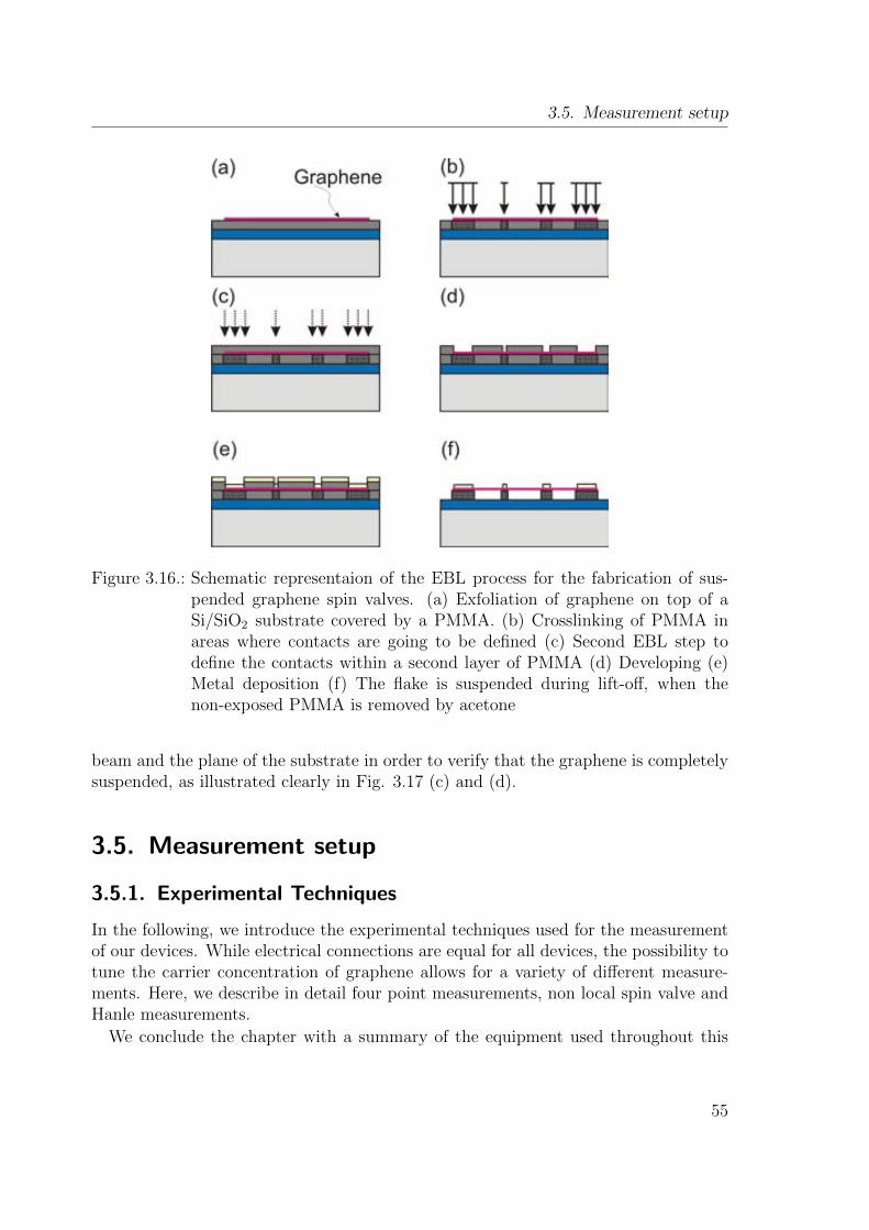
3.5. Measurement setup
Figure 3.16.: Schematic representaion of the EBL process for the fabrication of sus-pended graphene spin valves. (a) Exfoliation of graphene on top of aSi/SiO2 substrate covered by a PMMA. (b) Crosslinking of PMMA inareas where contacts are going to be defined (c) Second EBL step todefine the contacts within a second layer of PMMA (d) Developing (e)Metal deposition (f) The flake is suspended during lift-off, when thenon-exposed PMMA is removed by acetone
beam and the plane of the substrate in order to verify that the graphene is completelysuspended, as illustrated clearly in Fig. 3.17 (c) and (d).
3.5. Measurement setup
3.5.1. Experimental Techniques
In the following, we introduce the experimental techniques used for the measurementof our devices. While electrical connections are equal for all devices, the possibility totune the carrier concentration of graphene allows for a variety of different measure-ments. Here, we describe in detail four point measurements, non local spin valve andHanle measurements.
We conclude the chapter with a summary of the equipment used throughout this
55

3. Experimental Techniques and Methods
Figure 3.17.: SEM images of a suspended graphene sample (a) - (c): Images of a partic-ular sample taken under an angle of 70o between e-beam and substrate.In (a), the entire area of overexposed PMMA on top of the Si substrate isvisible as well as the four electrodes and the suspended graphene flake. In(c), a shadow is visible at the bottom of the trench below the flake, con-firming that the flake is completely suspended. (d) Same sample imagedunder an angle of 45o
thesis.
3.5.2. Four Point Measurements and the Electric Field Effect
The electrical resistance of a device is determined by applying a voltage over it andmeasuring the current flowing via the device, or vice versa. Throughout this thesis,we have generally used the second option, i.e. applying a bias current and measuringthe voltage drop along the device.
A straightforward method in order to achieve that is the two point configuration,where only two contacts are required for the measurement. In this way, not only theresistance of the device under test is measured but the resistance of the wires as well.Since the wires in this case partially consist of small junctions, the wire resistance canbe hundreds of Ohm.
The device resistance can be measured directly in four point configuration, as shownin Fig. 3.5.2 (a). Here, the bias current I is applied to the outer two contacts, whilethe voltage is measured between the inner two contacts.
56

3.5. Measurement setup
In order to measure the electric field effect, a voltage is applied between the p+
Si substrate and the ground. As discussed in section 2.8.3, the graphene and the Siact as two plates of a capacitor, with one or several dielectric materials in betweenthem. Sweeping the backgate voltage results in a variation of the numbers of carriersin graphene, as n = αVBG.
Experimentally, this can be demonstrated by fixing a source drain current I andmeasuring the voltage V across the sample while sweeping VBG. By using R = V/I aswell as ρ = R × (W/L), where W is the width and L the length of the flake betweenthe voltage contacts, it is possible to obtain the resistivity ρ as a function of VBG. wecan therefore plot the field effect as shown in Fig. 3.5.2 (b).
These measurements allow for a determination of the mobility of our samples. Incase of the example in the figure, the mobility is approx. 4500 cm2V−1s−1 at roomtemperature.
Figure 3.18.: (a) Experimental setup for four point measurement of field effect ofgraphene (b) Resistivity ρ4P as function of carrier density n
3.5.3. Non Local Spin Valve Measurements
We have introduced Non Local Spin Valve measurements in section 2.5 from a theoret-ical point of view. There, we have discussed a system consisting of two ferromagneticelectrodes on top of a non magnetic material.
However, in case of our graphene spin valves at least four electrodes are requiredin order to perform non local measurements, as shown in Fig. 3.19. Ideally, theouter two contacts of the devices consist of non magnetic materials. This way, we canneglect those contacts and focus only on the spin injection properties of the inner twoferromagnets. However, an additional lithography step is required for that, detrimentalto the qualtity of graphene. Therefore, we fabricate our devices with four ferromagneticelectrodes, as shown in section 3.4.
We connect the voltage and the current circuit as shown in Fig. 3.19. Here, thevoltage is measured on the left hand side of the device, while the current is applied on
57
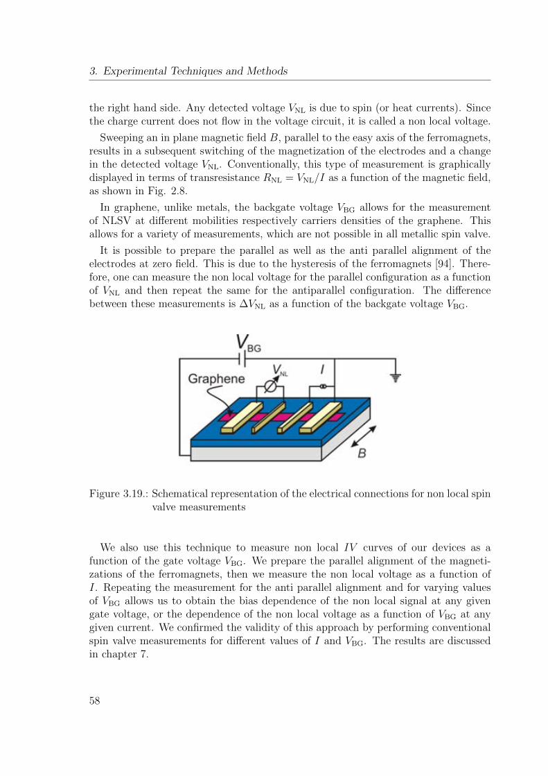
3. Experimental Techniques and Methods
the right hand side. Any detected voltage VNL is due to spin (or heat currents). Sincethe charge current does not flow in the voltage circuit, it is called a non local voltage.
Sweeping an in plane magnetic field B, parallel to the easy axis of the ferromagnets,results in a subsequent switching of the magnetization of the electrodes and a changein the detected voltage VNL. Conventionally, this type of measurement is graphicallydisplayed in terms of transresistance RNL = VNL/I as a function of the magnetic field,as shown in Fig. 2.8.
In graphene, unlike metals, the backgate voltage VBG allows for the measurementof NLSV at different mobilities respectively carriers densities of the graphene. Thisallows for a variety of measurements, which are not possible in all metallic spin valve.
It is possible to prepare the parallel as well as the anti parallel alignment of theelectrodes at zero field. This is due to the hysteresis of the ferromagnets [94]. There-fore, one can measure the non local voltage for the parallel configuration as a functionof VNL and then repeat the same for the antiparallel configuration. The differencebetween these measurements is ∆VNL as a function of the backgate voltage VBG.
Figure 3.19.: Schematical representation of the electrical connections for non local spinvalve measurements
We also use this technique to measure non local IV curves of our devices as afunction of the gate voltage VBG. We prepare the parallel alignment of the magneti-zations of the ferromagnets, then we measure the non local voltage as a function ofI. Repeating the measurement for the anti parallel alignment and for varying valuesof VBG allows us to obtain the bias dependence of the non local signal at any givengate voltage, or the dependence of the non local voltage as a function of VBG at anygiven current. We confirmed the validity of this approach by performing conventionalspin valve measurements for different values of I and VBG. The results are discussedin chapter 7.
58
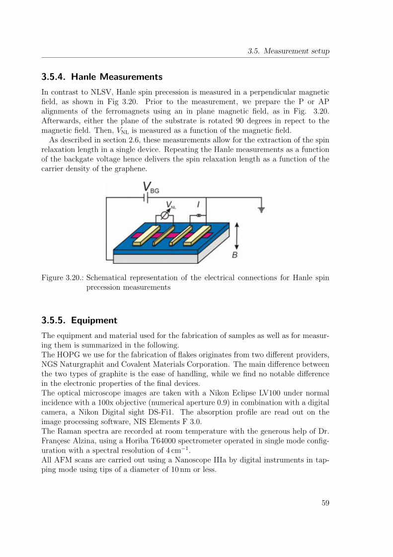
3.5. Measurement setup
3.5.4. Hanle Measurements
In contrast to NLSV, Hanle spin precession is measured in a perpendicular magneticfield, as shown in Fig 3.20. Prior to the measurement, we prepare the P or APalignments of the ferromagnets using an in plane magnetic field, as in Fig. 3.20.Afterwards, either the plane of the substrate is rotated 90 degrees in repect to themagnetic field. Then, VNL is measured as a function of the magnetic field.
As described in section 2.6, these measurements allow for the extraction of the spinrelaxation length in a single device. Repeating the Hanle measurements as a functionof the backgate voltage hence delivers the spin relaxation length as a function of thecarrier density of the graphene.
Figure 3.20.: Schematical representation of the electrical connections for Hanle spinprecession measurements
3.5.5. Equipment
The equipment and material used for the fabrication of samples as well as for measur-ing them is summarized in the following.The HOPG we use for the fabrication of flakes originates from two different providers,NGS Naturgraphit and Covalent Materials Corporation. The main difference betweenthe two types of graphite is the ease of handling, while we find no notable differencein the electronic properties of the final devices.The optical microscope images are taken with a Nikon Eclipse LV100 under normalincidence with a 100x objective (numerical aperture 0.9) in combination with a digitalcamera, a Nikon Digital sight DS-Fi1. The absorption profile are read out on theimage processing software, NIS Elements F 3.0.The Raman spectra are recorded at room temperature with the generous help of Dr.Francesc Alzina, using a Horiba T64000 spectrometer operated in single mode config-uration with a spectral resolution of 4 cm−1.All AFM scans are carried out using a Nanoscope IIIa by digital instruments in tap-ping mode using tips of a diameter of 10 nm or less.
59

3. Experimental Techniques and Methods
The EBL system used for the fabrication of the samples consists of an SEM moduleby Carl Zeiss together with a EBL module by Raith GmbH, a Raith 150-Two. Theaccelerating voltage for all EBL processes is 30 keV, using apertures of either 20 or120µm. The background pressure of the chamber is approx. 1×10⁻⁶ mbar. The SEMimages are taken at lower acceleration voltages between 2 and 10 keV either with theRaith or in a Quanta FEI.We carry out the deposition of the metal contacts in a electron beam evaporator byAJA International at a base pressure of approx. 1 × 10⁻⁷ Torr. At an acceleratingvoltage of 8 keV, it requires approx. 50 mA in order to evaporate cobalt, used as ma-terial for the contacts.The electrical connections to the sample are achieved by wirebonding 25µm thin alu-minium wires to the contact pads of the devices, using a wirebonder by Westbond.Electrical measurement are carried out in a continous flow cryostat by Janis systems.The magnetic field is applied using either a Lakeshore magnet with a maximum fieldof 1 T, or a GMW magnet with a maximum field of 180 mT. The current applied tothe sample is given by a current source K6221 by Keithley instruments. The voltagesare read out by a nanovoltmeter by Keithley, a K2182, which operates together withthe current source in delta mode. Alternatively, DC measurement were carried outusing the K6221 as current source, while reading out the voltage using an Agilent34410 multimeter.Finally, the backgate voltages are applied by using either a Keithley 2400 Current/Voltagesource or a Keithley 230 voltage source.
60

4. On the Theory of Spin DependentTunneling
4.1. Introduction
Throughout this chapter, we analyze in detail the tunneling process of electrons be-tween ferromagnetic and nonmagnetic electrodes based on an elementary model sys-tem. Especially, we discuss the bias dependence of this system, introducing basicconcepts which are important for the understanding of spin dependent transport.
The tunneling process of particles via a barrier, whose energy is larger than thatof the particle itself, is one of the textbook examples of quantum mechanics (seee.g. [95, 96]). As such, it has repeatedly attracted the attention of the scientificcommunity. For instance, the transmission of conduction electrons from one metalinto another via an insulating layer can be understood as a resonant tunneling processand has attracted considerable attention in the 1960s [97, 98, 99, 100].
If additionally one of the electrodes in such a junction is ferromagnetic, then thetunneling process is spin dependent and the tunneling current spin polarized. Giventhe elementary nature of the process, it is surprising to find that important propertiesof spin-dependent tunneling (SDT) are not understood to the current day.
Interest in the topic of SDT was raised by a series of seminal experiments by Meser-vey and Tedrow [1, 2]. They studied tunneling in FM/I/SC junctions, where I standsfor an insulator and SC for an superconductor. In a large magnetic field, the densityof states of the SC is Zeeman splitted. This allowed for a determination of the spinpolarization of a variety of 3d ferromagnets for I = Al2O3 by measuring the bias de-pendence of such a junction. It became immediately obvious that the experimentalresults did not agree with theoretical predictions of the process, which were solelybased on the DOS of the FMs at the Fermi level. These predictions did not provideneither the correct magnitude of the spin polarization nor its sign.
As a solution, Stearns proposed that only itinerant electrons contribute to the tun-neling process, requiring to take into account the specific band structure of the 3d-transition metals: Dispersive s-bands are hybridized with more localized d-bands [101].Although these d-bands have a strong weight at the Fermi energy, Stearns argumentedthat due to the different effective masses, the transport will be dominated by the nearlyfree s-electrons.
As soon as a fabrication technique for pinhole free Al2O3 tunnel barriers became
61
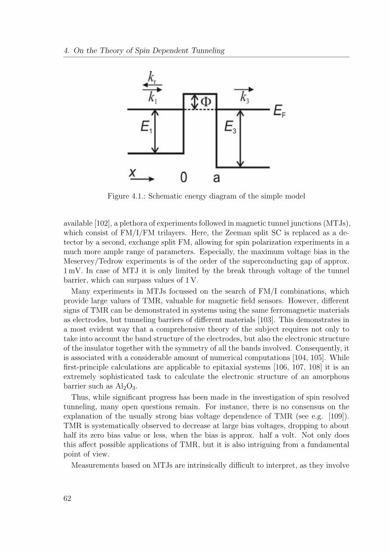
4. On the Theory of Spin Dependent Tunneling
Figure 4.1.: Schematic energy diagram of the simple model
available [102], a plethora of experiments followed in magnetic tunnel junctions (MTJs),which consist of FM/I/FM trilayers. Here, the Zeeman split SC is replaced as a de-tector by a second, exchange split FM, allowing for spin polarization experiments in amuch more ample range of parameters. Especially, the maximum voltage bias in theMeservey/Tedrow experiments is of the order of the superconducting gap of approx.1 mV. In case of MTJ it is only limited by the break through voltage of the tunnelbarrier, which can surpass values of 1 V.
Many experiments in MTJs focussed on the search of FM/I combinations, whichprovide large values of TMR, valuable for magnetic field sensors. However, differentsigns of TMR can be demonstrated in systems using the same ferromagnetic materialsas electrodes, but tunneling barriers of different materials [103]. This demonstrates ina most evident way that a comprehensive theory of the subject requires not only totake into account the band structure of the electrodes, but also the electronic structureof the insulator together with the symmetry of all the bands involved. Consequently, itis associated with a considerable amount of numerical computations [104, 105]. Whilefirst-principle calculations are applicable to epitaxial systems [106, 107, 108] it is anextremely sophisticated task to calculate the electronic structure of an amorphousbarrier such as Al2O3.
Thus, while significant progress has been made in the investigation of spin resolvedtunneling, many open questions remain. For instance, there is no consensus on theexplanation of the usually strong bias voltage dependence of TMR (see e.g. [109]).TMR is systematically observed to decrease at large bias voltages, dropping to abouthalf its zero bias value or less, when the bias is approx. half a volt. Not only doesthis affect possible applications of TMR, but it is also intriguing from a fundamentalpoint of view.
Measurements based on MTJs are intrinsically difficult to interpret, as they involve
62

4.2. Free Electron Tunneling
Figure 4.2.: (a) Tunneling from NM into FM and (b) from FM into NM
electrons tunneling out of one ferrromagnetic electrode into another one, and spinpolarizations of both electrode participate in a non trivial way. As a consequence,alternative experimental and theoretical methods are required in order to study theeffects of the ferromagnetic electrodes separately. This possibility is given in non localspin valve structures (see section 2.5). Here, SDT can be studied by directly measuringthe polarization of the single FM/I interface, as in the Meservey/Tedrow technique,while avoiding the experimental limitations imposed by the superconducting detector.
The data obtained with such devices show a strong asymmetry about zero bias [94],which we analyze with a theoretical approach based on an analytical free-electronmodel. The model uses a minimum of elements that should be present in any co-herent tunneling event. Despite its simplicity, our model qualitatively explains theexperimental observations.
4.2. Free Electron Tunneling
In order to describe the process, we make on the following assumptions:
1. Our model is based on an analytical solution of the stationary, one-dimensionalSchrodinger equation using a rectangular shaped potential. The potential char-acterizes the insulating layer, while the electrons in the metal electrodes are seenas free particles. Our simple one electron picture can be extended by using thedensity of states for free electrons and by including a bias dependence of thebarrier shape.
2. The magnetic materials are supposed to act as perfect Stoner FMs, which meansthat there are different bands for majority and minority spin that are character-ized by different wave numbers.
63

4. On the Theory of Spin Dependent Tunneling
Figure 4.3.: Schematic representation of the extended model
3. We use the two-current model of Mott [37], stating that the electric conductivityof a magnetic material consist of a sum of the conductivities of spin up respec-tively spin down electrons, σNM = σ↑ + σ↓. This implies that spin flips duringthe tunneling process are neglected.
The Stoner model of ferromagnetism and the two-current model are discussed inmore detail in chapter 2.
It is convenient to first derive a general expression for the tunneling probability of asingle electron without regarding spin, only depending on the energy before and aftertunneling as well as on the work function of the barrier. A more detailed derivation ofthis exercise can be found in [96]. Then, it is straightforward to obtain the differentprobabilities for spin up and spin down by considering the specific Emaj and Emin andthe overall current by summing up the two independent spin contributions.
The potential landscape is depicted in Fig. 4.1. The electrons in regions 1 and 3 arecharacterized solely by their energies E1 respectively E3, the potential barrier by itswidth a and its work function Φ = V −E1. The transmission probability T is definedas the ratio of the incident to transmitted current density and is obtained by solvingthe 1D, time independent Schrodinger equation. The solutions have the general formψj = aje
−ikjx + bjeikjx for j = 1, 3 and ψ2 = a2e
−k2x + b2ek2x in region two. Here, the
wave vectors kj are defined by E1,3 = ~2k21,3/2m in region 1 and 3 and by Φ = ~2k22/2min region two.
Now, we use the boundary conditions at the interfaces between metal and insulatorat x = 0 and x = a. Additionaly, we take into account that b3 = 0, since we considerparticles coming in from the left, thus only transmitted waves exist in region 3, onthe right hand side of the barrier. Solving the resulting linear system of equations weobtain for the transmission probability T
T =4k1k2
(k21 + k22)
4k2k3(k23 + k22)
e−2k2a (4.1)
64

4.2. Free Electron Tunneling
Figure 4.4.: Transmission probability as a function of E3/φ, exhibiting a peak atE3/φ = 1
Here, we have used e−2k2a 1, as we treat the weak transmission limit, which is rea-sonable for Φ of the order of an electronvolt and a barrier thickness a in the nanometerrange.
It is straightforward to extend our results to a system where one of the electrodesis ferromagnetic by using assumptions 2 and 3. Tunneling from NM to FM is shownschematically in Fig. 4.2 (a), and tunneling from a FM into NM in Fig. 4.2 (b). Here,an additional bias voltage V is introduced. The bottom of the bands of the FMs areshifted by the exchange interaction Eex for majority (up) and minority (down) spin.
For tunneling of electrons from NM to FM, the energies read E↑,↓1 = Emaj,min + eV
and E↑,↓3 = E3 while for tunneling from FM to NM, E↑,↓1 = Emaj,min and E↑,↓3 = E3+eV .With the corresponding wave number k, the transmission probabilities for spin up andspin down in each case can be obtained from eq. 4.1. The total transmission is givenby T = T ↑ + T ↓.
Now, we can study the bias dependence of the polarization of the transmitted tun-neling current. It is defined as
P =j↑3 − j
↓3
j↑3 + j↓3(4.2)
Here, j↑,↓3 are the current densities on the right hand side of the barrier. Withthe transmission coefficient t of the barrier, these current densities are given by
65

4. On the Theory of Spin Dependent Tunneling
Figure 4.5.: (a) Polarization of the Current and (b) T ↑ and T ↓ as a function of E3
j↑,↓3 = −(e~k↑,↓3 /m)∣∣t↑,↓∣∣2. Therefore, the polarization P can be written as
P =
(k↑
k↑2 + k22− k↓
k↓2 + k22
)/
(k↑
k↑2 + k22+
k↓
k↓2 + k22
)=
( √E↑
E↑ + Φ−√E↓
E↓ + Φ
)/
( √E↑
E↑ + Φ+
√E↓
E↓ + Φ
)(4.3)
where we distinguish between two different cases: When tunneling out of NM intoFM, k↑,↓ = k↑,↓3 , while in the case of tunneling from FM to NM, k↑,↓ = k↑,↓1 . Inthe former case, k↑,↓ depends on the bias V , but not in the latter one. Moreover,the polarization of the tunneling of electrons is different from the polarization of theelectrons of the Fermi level of the FM, which in a free electron model is given byPFM = (k↑ − k↓)/(k↑ + k↓).
Finally, we extend our model by taking into account two additional features. First,we include the DOS of free electrons in eq. 4.3, which consists of a factor D(Ei) = kiin equation P . Second, it is known that applying a bias voltage across a tunneling
66

4.3. Discussion
barrier alters the shape of its potential. Here, we follow a method developed byHolm [97] and Simmons [98], which consist of approximating the tunneling barrierby its average height. Assuming a uniform voltage drop, the shape of the barrier istrapezoidal, meaning that it can be approximated by a rectangular barrier lowered bya factor − e
2V with respect to the undisturbed height. In our derivation we therefore
substitute Φ 7→ Φ0 − e2V . Since k2 ∝
√Φ, this means that the polarization P , given
by eq. 4.3, is affected by the substitution as well. Both extensions of the model areschematically shown in Fig. 4.3.
4.3. Discussion
In the following, we discuss the polarization of the current as predicted by our sim-ple model. Furthermore, we compare this prediction with those obtained from moreelaborated models.
First, we focus on the change of sign of P that has been observed experimentally[94]. It can be understood by considering the transmission probability T given byEq. 4.1 in the case of electrons tunneling out of NM into FM. In Fig. 4.4, we plotT as a function of E3/Φ. It becomes visible that the transmission reaches a peakwhenever the wavevector of the transmitted wave matches that of the evanescent one[94], E3 = Φ. Here, E↑,↓3 = Emaj,min + eV . This means that the transmission for thespin up and down channel, respectively, peaks at V max
maj,min = (Φ− Emaj,min)/e.Together with the exchange splitting of the spin subbands, this leads to the change
of sign in the polarization P . As the bottom of the two spin subbands are shiftedby Eex, the transmission probability for spin up and down reaches its maximum atdifferent bias voltages.
An example is shown in Fig. 4.5, where we have simulated the tunneling of electronsfrom Aluminium into Permalloy via a tunneling barrier of 1 nm thickness and 1.2 eVpotential height. The polarization P of the current as given by eq. 4.3 is shown in Fig.4.5 (a), while the transmission probabilities T ↑,↓ for the majority and minority bandsare shown as a function of E3 in Fig. 4.5 (b). For majority spin, E↑3 = 2.25 eV + eV ,while for minority spin, E↓3 = 0.5 eV + eV .
At zero bias voltage, the transmission probability for the majority spin type ishigher than that of the minority. For spin up, it is given by T ↑ = T (2.25 eV), while forspin down T ↓ = T (0.5 eV). However, with increasing bias, T ↑ continually decreases,while T ↓ increases with increasing bias (until it peaks at 0.7 eV, so that E↓3 = Φ). Atapproximately 0.11 eV, the transmission probabilities for both channels are equal andfor higher bias voltages, T ↑ < T ↓, leading to the change in sign in P .
Despite the simplicity of our approach, we are thus able to qualitatively explainthis feature with our model, which is only based on elementary concepts of quantummechanics. This shows that the bias dependence of the polarization of the current inthese systems cannot be understood in a straightforward way, as it exhibits a rather
67

4. On the Theory of Spin Dependent Tunneling
Figure 4.6.: (a) Comparision of P as predicted by the different model (b) Schematicrepresentation of the model including DOS and (c) including DOS andbias dependent potential barrier
unintuitive behavior.
However, the simple model fails to capture the dependence of P on the bias voltageV for electrons tunneling from FM into NM.
In the following, we show that the extended versions of the model deliver a moreaccurate prediction of P . In Fig. 4.6 we compare the different versions of P , wherewe use the same values for Emaj, Emin and Φ0 as above. It can be seen that takinginto account the DOS of the electrons leads to a value of approx. 38 % at zero biasfor the calculated polarization, which is close to the experimentally observed one [94].However, a decaying spin polarization for negative values of V , i.e. for tunneling ofelectrons from NM into FM, can only be predicted by considering the deformationof the shape of the barrier due to the applied bias voltage. The same conclusion hasbeen drawn in case of SDT between FMs and semiconductors across a Schottky barrier[110].
Thus, by extending our model with a modulated shape of the potential barrier, wequalitatively explain the tunneling process from ferro- into nonmagnetic electrode aswell. One might assume that the only missing ingredient to a full description of thesystem would be finding the appropriate shape of the potential barrier. Unfortunately,the realistic shape of such potential barriers is poorly known and it has been pointedout[111] that such a model is very sensitive to the shape of the potential barrier.
68

4.4. Conclusion
4.4. Conclusion
Throughout this chapter, we have developed a simple one electron model of spindependent tunneling in FM/I/NM junctions, based on an analytical solution of theSchrodinger equation. We have focussed on the bias dependence of the polarizationof the current passing through these junctions. The predictions are in agreementwith experimental data, exhibiting a change of sign when tunneling takes place fromnonmagnetic into ferromagnetic material. Our approach may serve as a first approx-imation of the process, although it is clear that a comprehensive description has toincorporate a variety of data, such as the band structure of both the electrodes andthe insulator.
Our simple model is thus unable to render all of the complexity inherent to non-idealinterfaces, scattering or complex band structures. However, it qualitatively explainsthe experimental observations and shows that complex behavior of the polarization asa function of the bias voltage is intrinsic to tunneling and is highly sensitive to theratio between the electron wave numbers inside and outside of the barrier region.
69


5. Electrical Detection of SpinPrecession in freely-suspendedGraphene Spin Valves
5.1. Introduction
In this chapter, we present measurements on freely-suspended graphene spin valves[68]. We achieve electrical spin injection and detection using cobalt electrodes anda non local spin valve geometry. The devies are fabricated with a single electronbeam resist process, minimizing both the fabrication steps and the number of ag-gressive chemicals used, greatly reducing contamination and increasing the yield ofhigh-quality, mechanically stable devices. As-grown devices can present mobilities ex-ceeding 104 cm2 V−1s−1 at room temperature and, because the contacts deposited ongraphene are only exposed to acetone and isopropanol, the method is compatible withalmost any contacting material. We study spin accumulation and spin precession inour non local spin valves. Fitting of Hanle spin precession data in bilayer and multi-layer graphene yields a spin relaxation time of 125-250 ps and a spin diffusion lengthof 1.7− 1.9µm at room temperature.
5.2. Spin Injection in Graphene
Graphene and few layer graphene (FLG) and related materials are very promisingfor nanoelectronics [21, 112, 113] and are considered ideal candidates to transportspin information in future spintronic devices [58, 59, 114]. Long spin lifetimes τsfand relaxation lengths λsf can be expected due to small intrinsic spin-orbit couplingand the lack of hyperfine interaction with the predominant carbon nuclei 12C, whichhas no spin [58, 59, 114]. However, although predictions indicate that λsf shouldexceed tenths or even hundredths of micrometers [58, 59], the largest reported valueto date is λsf ∼ 5µm for bilayer graphene (BLG) [67]. These results are observedusing tunneling contacts at low temperatures (20 K), where relatively long τsf ∼ 6 nshave been measured. At room temperatures, τsf usually drops to a few hundredpicoseconds and is in the nanosecond range only in samples with very low mobility(µ = 300 cm2V−1s−1 in Ref. [115]). For single layer graphene (SLG), the results are
71

5. Electrical Detection of Spin Precession in freely-suspended Graphene Spin Valves
Figure 5.1.: (a) SEM image of the a suspended graphene flake between two ferro-magnetic electrodes (b) Optical microscope image of SLG, indicated bydashed lines, over three trenches in the PMMA, with electrical connectionsfor four point measurements
even more discouraging and state-of-the art devices show λsf < 3µm and τsf < 1 ns at10 K [55, 67, 116].
The reasons for the discrepancy between theory and experiment have yet to beclarified. Most experiments are carried out in graphene with relatively low µ in therange of 500 − 2000 cm2V−1s−1, where the spin relaxation process has been ascribedto the Elliot-Yafet mechanism [65]. A simple extrapolation to µ = 2×105 cm2 V−1s−1,assuming that the Elliot-Yafet mechanism is still valid, results in λsf ∼ 100µm [65],which is very promising for applications and close to the predictions. However, reports[66] on graphene decorated with gold are at odds with this notion. Therefore, it hasbeen suggested that the spin relaxation could result from a combination of Elliot-Yafetand Dyakonov-Perel processes [58, 59, 117], a point we discuss further in section 2.9.
The interaction between graphene and the substrate, usually SiO2, has been iden-tified as one of the reasons for the low mobilities of spintronic graphene devices [118].The substrate contributes charged impurities that increase the scattering of carriersand creates puddles of holes and electrons that reduce the mobility [119]. It couldalso result in small locally-strained regions where spin-orbit interaction is enhanced[58, 59]. The effects of the substrate have been recognized in early charge transportstudies, leading to the fabrication of freely-suspended graphene devices [118, 120],which, combined with the development of cleaning methods [92, 93, 121], resulted inmobilities well beyond 105 cm2 V−1s−1 [118, 120].
In order to gather knowledge on spin relaxation processes and possibly enhancespin lifetimes, it is important to fabricate suspended graphene spintronic devices.Unfortunately, the accepted fabrication technique for suspended structures cannotbe used for this purpose. Suspended structures are usually created in three stepsthat consist of depositing graphene onto a sacrificial SiO2 layer, contacting graphene
72

5.3. Results and Discussion
with Cr/Au electrodes and then etching SiO2 away using a hydrofluoric acid (HF)solution [118, 120]. Here, HF is an extremely aggressive acid that attacks most metals[122, 123], including the ferromagnets (Co, Ni, Fe, etc) that are essential for electricalspin injection and detection. As a consequence, it is mandatory to eliminate the HFetching step to fabricate suspended graphene spintronic devices. Additionally, it isdesirable to minimize the fabrication steps and the chemicals to which graphene isexposed in order to achieve the largest possible carrier mobility.
Here, we demonstrate spin transport in suspended graphene devices using a uniquemethod that overcomes the drawbacks mentioned above. The fabrication process ofthese devices is described in detail in chapter 3.4.5. The advantages of the process be-come clear when comparing it with the fabrication method for conventional graphenespin valves on a Si/SiO2 substrate (see section 3.4.3). The conventional method re-quires the use of PMMA as a positive resist, a developer such as MIBK and acetone andisopropanol during lift-off. Therefore, the ultimately optimized method to fabricatesuspended graphene devices should add one lithography step to define where grapheneshould be suspended, use only PMMA as a resist and avoid adding any solvents otherthan the previously listed. The process presented here fulfills these specifications.
Our fabrication method is highly versatile allowing us to easily introduce modifica-tions in the device design, including the number of contacts, the separation betweenthem and the height of the dielectric. Because it is an acid-free method with a minimalnumber of steps, it is compatible with any contact material and capable of producingvery high quality devices, even without any further processing.
Alternative approaches have been demonstrated which enable acid free fabricationof suspended graphene samples as well [69, 124, 125]. These methods however requirethe use of polymers other than PMMA, namely positive lift-off resists such as LOR,and a variety of chemicals.
5.3. Results and Discussion
A typical device is shown in Fig. 5.1 (b), and measurements of the same device arepresented in Fig. 5.2. The device consists of a graphene monolayer with four contactsand three suspended graphene regions between them. The resistivity and mobilityof the device, without any post fabrication processing, is plotted as a function ofcarrier density n. A sharp resistivity peak (Fig. 5.2 (a)) close to backgate voltageVBG = 0 V with a soft p doping (n ∼ 1011 cm−2) is observed. The mobility is wellabove 5× 103 cm2 V−1s−1 and exceeds 2× 104 cm2 V−1s−1 for n = 1011 cm−2 at roomtemperature (Fig. 5.2 (b)). This is an excellent starting point when compared withother fabrication methods and implies that argon/hydrogen annealing [92, 121] orcurrent annealing [93] can likely be used to obtain ultrahigh mobility samples.
We also extract the residual carrier density n0 of our devices. Charged impurities inthe vicinity of graphene induce a non-zero value of n and the total carrier concentra-
73

5. Electrical Detection of Spin Precession in freely-suspended Graphene Spin Valves
Figure 5.2.: (a) Resistivity of a suspended graphene monolayer over a 1µm trench atroom temperature and 77 K. The Dirac-point of the sample is close toVBG = 0 V with a soft p doping (n0 ∼ 1011cm−2). An optical microscopeimage of the device is shown in Fig. 5.1. (b) Mobility of the sample.
tion can be approximated as [50] ntot = (n20 + n(VBG)2)1/2. Fitting the curves in Fig.
5.2 delivers n0 = 1.4 × 1011 cm−2 at room temperature and n0 = 8.7 × 1010 cm−2 at77 K, indicating the high quality of our as-processed devices. The room temperatureresidual carrier concentration is indicated by gray areas in Fig. 5.2. For n < n0, themobilities given by formula 2.61 have to be disregarded.
Figure 5.3 (b) shows a device based on FLG with eight Co contacts (100-200 nmwide) and suspended regions between them. By using the four inner contacts we per-formed non local spin injection/detection measurements [8, 16, 55]. The non localresistance RNL = (V + − V −)/I presents clear spin signatures (Fig. 5.3 (a)) as anin plane magnetic field B along the ferromagnetic electrodes is swept up (green cir-cles) and down (blue circles). The various values of RNL are associated to differentmagnetization alignments of the contacts as represented with arrows [126]. A change
74

5.3. Results and Discussion
∆RNL = 12.5 Ω is observed when the central electrodes switch from parallel to an-tiparallel states. As in Ref. [126], the switching sequence is determined by the widthof the electrodes, which leads to distinct switching fields that we have characterizedin prior experiments.
Figure 5.3.: (a) Non local spin resistance RNL in a multiterminal device as the magneticfield B is swept up (green symbols) or down (blue symbols) along theferromagnetic electrodes (Co). Measurements are performed at VBG = 0 Vand room temperature. Inset: Optical microscope image of the device andthe configuration of the electrodes. The flake is indicated by the dashedlines.
For SLG and BLG, we observe a similar behavior as the one shown in Fig. 5.3,although the magnitude of the spin signal tends to be somewhat smaller for deviceswith similar dimensions. An example is shown in Fig. 5.4, where data of a BLG deviceis presented. Spin valve measurements exhibit a non local resistance of ∆RNL = 6 Ω(Fig. 5.4 (a)), while the observation of Hanle spin precession under a perpendicularB (Fig. 5.4 (b)) confirms the presence of a spin signal and provides a direct wayto obtain τsf [8]. Quantitatively, the response to the perpendicular B resulting fromspin precession can be described with a one dimensional model which combines spindiffusion, precession and relaxation [8, 16, 55]. The fit indicates τsf ≈ 1.9µm andτsf ≈ 125 ps. These values are similar to those found in SLG with transparent contacts[127] and in BLG spintronic devices with the highest mobility reported [115].
Additionally, we note that the height of the spin signal is three orders of magnitudelarger when comparing our devices to graphene spin valves using transparent contacts[127]. As we show in chapter 6, we attribute this increase to the deposition of anamorphous carbon layer at the interface between graphene and Co. This is due to theoverexposure required for the crosslinking of the PMMA below graphene [128]. How-
75
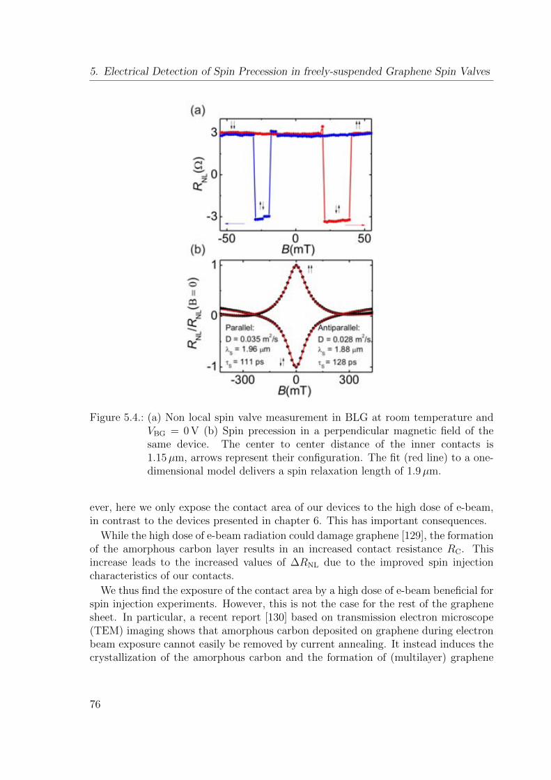
5. Electrical Detection of Spin Precession in freely-suspended Graphene Spin Valves
Figure 5.4.: (a) Non local spin valve measurement in BLG at room temperature andVBG = 0 V (b) Spin precession in a perpendicular magnetic field of thesame device. The center to center distance of the inner contacts is1.15µm, arrows represent their configuration. The fit (red line) to a one-dimensional model delivers a spin relaxation length of 1.9µm.
ever, here we only expose the contact area of our devices to the high dose of e-beam,in contrast to the devices presented in chapter 6. This has important consequences.
While the high dose of e-beam radiation could damage graphene [129], the formationof the amorphous carbon layer results in an increased contact resistance RC. Thisincrease leads to the increased values of ∆RNL due to the improved spin injectioncharacteristics of our contacts.
We thus find the exposure of the contact area by a high dose of e-beam beneficial forspin injection experiments. However, this is not the case for the rest of the graphenesheet. In particular, a recent report [130] based on transmission electron microscope(TEM) imaging shows that amorphous carbon deposited on graphene during electronbeam exposure cannot easily be removed by current annealing. It instead induces thecrystallization of the amorphous carbon and the formation of (multilayer) graphene
76

5.4. Conclusion
patches due to the high temperatures involved.During the fabrication of our devices, we do not expose the graphene in between
the contacts. Therefore, we expect that we deposit amorphous carbon only in thecontact areas, and higher mobilities than those presented here can likely be obtainedby current annealing of the unexposed graphene.
5.4. Conclusion
In summary, we have performed electrical detection of spin accumulation and of spinprecession in freely-suspended graphene flakes from which we can estimate spin relax-ation lengths and times. We observe non local spin signals as high as ∆RNL ∼ 10 Ω.
The device fabrication involves a minimal number of steps and chemicals and, be-cause it is acid-free, it can be adapted to any contacting material. Mobilities as high as2× 104 cm2 V−1s−1 for n = 1011 cm−2 are observed at room temperature without anypost fabrication processing. Argon/hydrogen and current annealing can be used toobtain ultrahigh mobility samples that will open the way for a detailed understandingof the spin relaxation mechanisms in graphene.
We expect that the demonstration of clean suspended graphene devices in few stepswith minimal number of chemicals is not only important for the spintronics community,but also for those interested in graphene nanomechanics [131] and future research inpseudomagnetic fields and the modification of the graphene transport properties dueto strain [70, 132].
77


6. Enhanced Spin Accumulation inGraphene Spin Valves
6.1. Introduction
We demonstrate a large enhancement of the spin accumulation in monolayer graphenefollowing electron-beam induced deposition of an amorphous carbon layer at theferromagnet-graphene interface. The enhancement is 104-fold when graphene is de-posited onto PMMA and exposed with sufficient e-beam dose to crosslink the PMMA,and 103-fold when graphene is deposited directly onto SiO2 and exposed with identicaldose. We attribute the difference to a more efficient carbon deposition in the formercase due to an increase in the presence of compounds containing carbon, which arereleased by the PMMA. The amorphous carbon interface can sustain large currentdensities without degrading, which leads to very large spin accumulations close to1 mV at room temperature.
6.2. Motivation
Graphene has attracted the attention of the spintronics community due to the longspin lifetimes and long relaxation lengths expected from its small intrinsic spin orbitinteraction and the lack of hyperfine interaction with the most abundant carbon nuclei12C [20, 133], which we discuss in section 2.9 and chapter 5. Here, we instead focus onthe interface and spin injection properties of our graphene non local spin valve devices.If large spin accumulation and large pure spin currents are achieved, NLSVs can beused to study spin torque switching [13] or spin Hall effects [134]. We demonstratespin accumulations ∆VNL ∼1 mV, which are among the largest values reported in anymaterial.
Depending on the interface characteristics between the FM and graphene, grapheneNLSVs have been classified into three types: those having Ohmic, pinhole or tunnelingcontacts [135]. As shown in chapter 2.5, the spin dependent voltage measured at thedetector depends on the ratio between the contact resistances and the spin resistancesof the materials.
In case of the tunnel junctions, the spin accumulation in the graphene is given byEq. 2.34. Although the magnitude of ∆RNL is much higher (∼ 100 Ω) than in theother cases [135], the maximum spin current density is limited by two factors. Firstly,
79
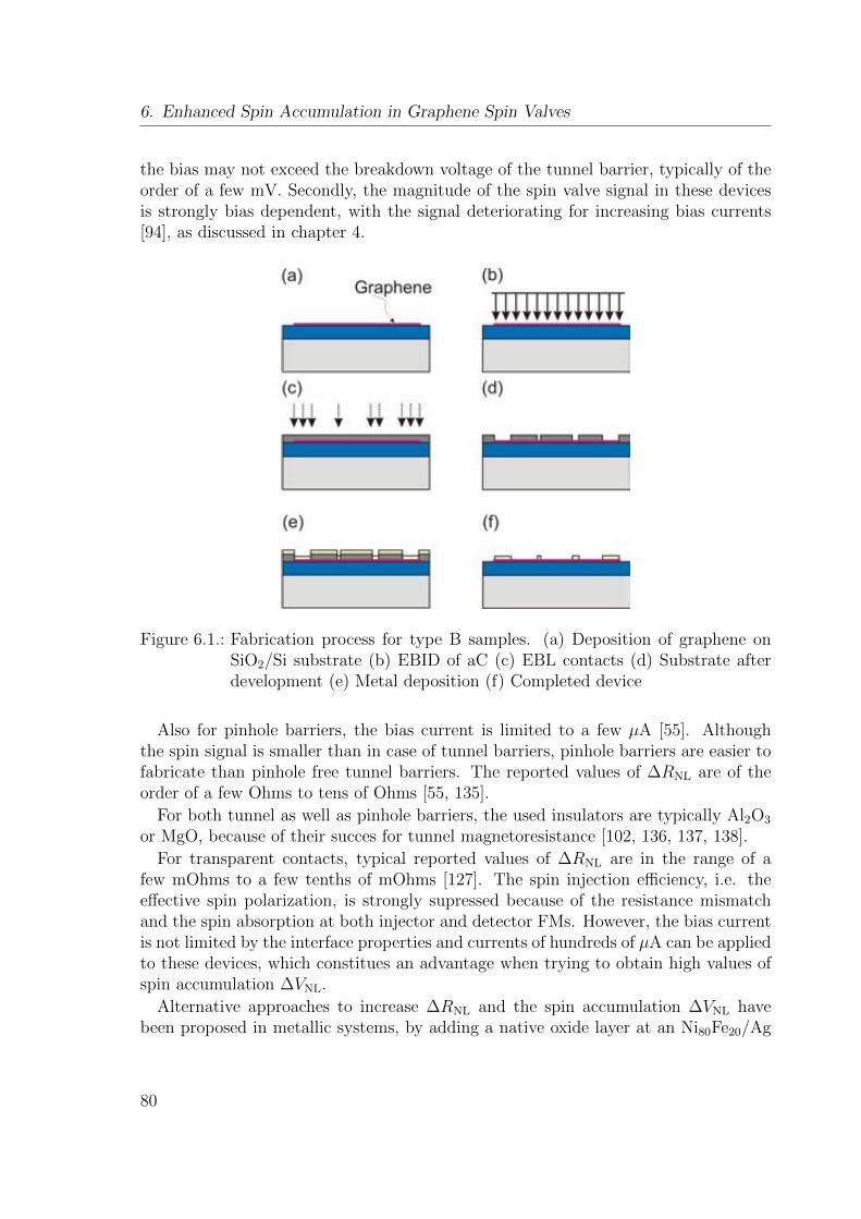
6. Enhanced Spin Accumulation in Graphene Spin Valves
the bias may not exceed the breakdown voltage of the tunnel barrier, typically of theorder of a few mV. Secondly, the magnitude of the spin valve signal in these devicesis strongly bias dependent, with the signal deteriorating for increasing bias currents[94], as discussed in chapter 4.
Figure 6.1.: Fabrication process for type B samples. (a) Deposition of graphene onSiO2/Si substrate (b) EBID of aC (c) EBL contacts (d) Substrate afterdevelopment (e) Metal deposition (f) Completed device
Also for pinhole barriers, the bias current is limited to a few µA [55]. Althoughthe spin signal is smaller than in case of tunnel barriers, pinhole barriers are easier tofabricate than pinhole free tunnel barriers. The reported values of ∆RNL are of theorder of a few Ohms to tens of Ohms [55, 135].
For both tunnel as well as pinhole barriers, the used insulators are typically Al2O3
or MgO, because of their succes for tunnel magnetoresistance [102, 136, 137, 138].
For transparent contacts, typical reported values of ∆RNL are in the range of afew mOhms to a few tenths of mOhms [127]. The spin injection efficiency, i.e. theeffective spin polarization, is strongly supressed because of the resistance mismatchand the spin absorption at both injector and detector FMs. However, the bias currentis not limited by the interface properties and currents of hundreds of µA can be appliedto these devices, which constitues an advantage when trying to obtain high values ofspin accumulation ∆VNL.
Alternative approaches to increase ∆RNL and the spin accumulation ∆VNL havebeen proposed in metallic systems, by adding a native oxide layer at an Ni80Fe20/Ag
80

6.3. Amorphous Carbon as Interface Material
interface [139] or by increasing confinement [140] and in graphene by adding a thinCu layer at the FM/graphene interface [141].
6.3. Amorphous Carbon as Interface Material
In the present work, we investigate FM/aC/graphene junctions as a spin polarizer,where aC stands for amorphous carbon. Amorphous carbon is deposited with highresolution using a focused electron-beam that decomposes molecules, such as hydro-carbons, that are then adsorbed on graphene. This process, known as electron-beaminduced deposition (EBID), is well established [142] and has been used, for example,to fabricate complex carbon structures [143], conducting bridges [144], and low re-sistance contacts with nanotubes [145]. Carbon precursors can either be introducedexternally using a gas source or simply be present as residual hydrocarbons at thebackground pressure of a scanning electron microscope (SEM) chamber [142]. Car-bon deposition from residual hydrocarbons in graphene was recently demonstrated bydirect visualization in a transmission electron microscope [130].
Figure 6.2.: Device layout, lateral (a) and top (b) views. Four ferromagnetic electrodesare in contact with graphene. The dielectric consists of 440 nm of SiO2
for type A and B devices, and 285 nm of SiO2 plus 200 nm of PMMA fortype C devices (see text). A layer of amorphous carbon is deposited withEBID at the interface between graphene and Co for type B and C devices.
In short, exposing graphene to e-beam radiation leads to the deposition of aC inthe exposed area. Keeping this in mind, we consider the fabrication process of oursuspended graphene devices, as described in chapter 3.4.5. While crosslinking thePMMA, we expose the graphene to a dose more than 20 times higher than the doserequired for regular electron beam lithography. We can therefore assume that duringthis step an aC layer is deposited on graphene, which then acts as intermediate layer,once the ferromagnetic material is deposited.
81

6. Enhanced Spin Accumulation in Graphene Spin Valves
In order to test this assumption, we have fabricated three different types of samples,in the following referred to as type A, B and C. Type A devices are reference sam-ples with transparent, Ohmic contacts, as described in chapter 3.4.3 and reported inprevious studies [146, 147]. The fabrication process of type B devices is schematicallyshown in Fig. 6.1. It differs from the type A fabrication process in step (b), exposureof graphene with a dose of 9000µC/cm2. This dose is large enough to deposit a thinlayer of aC at the residual pressure of our system [142, 143, 144, 145], which is in the10−6 Torr range. It is also the dose needed to crosslink PMMA. Type C devices aresamples fabricated using crosslinked PMMA as substrate, as described in section 3.4.4.Therefore, type A devices are standard graphene spin valves on a Si/SiO2-substrate,for type B samples we introduce an additional aC deposition step and type C sam-ples are fabricated using the additional step as well as being fabricated on crosslinkedPMMA as a substrate. This is schematicallly shown in Fig. 6.2 (a), where the di-electric consists of 440 nm of SiO2 for type A and B samples, and of 285 nm of SiO2
and 200 nm of PMMA for type C samples. Moreover, the aC layer between FM andgraphene is only present for type B and C samples.
Figure 6.3.: (a) SEM image of a device, the scale bar equals 1µm (b) NLSV measure-ment for a reference device with transparent contact (type A)
The use of PMMA as high-κ dielectric substrate for graphene has been reportedpreviously [84], but it can also be used for the fabrication of insulating [63, 85] ofhydrophobic layers [148]. More important, it increases the presence of carbon richmolecules in the EBL system during EBID, changing the dynamics of the aC depositionprocess.
82
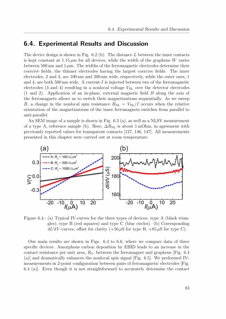
6.4. Experimental Results and Discussion
6.4. Experimental Results and Discussion
The device design is shown in Fig. 6.2 (b). The distance L between the inner contactsis kept constant at 1.15µm for all devices, while the width of the graphene W variesbetween 500 nm and 1µm. The widths of the ferromagnetic electrodes determine theircoercive fields, the thinner electrodes having the largest coercive fields. The innerelectrodes, 2 and 3, are 100 nm and 200 nm wide, respectively, while the outer ones, 1and 4, are both 500 nm wide. A current I is injected between two of the ferromagneticelectrodes (3 and 4) resulting in a nonlocal voltage VNL over the detector electrodes(1 and 2). Application of an in-plane, external magnetic field B along the axis ofthe ferromagnets allows us to switch their magnetizations sequentially. As we sweepB, a change in the nonlocal spin resistance RNL = VNL/I occurs when the relativeorientation of the magnetizations of the inner ferromagnets switches from parallel toanti-parallel.
An SEM image of a sample is shown in Fig. 6.3 (a), as well as a NLSV measurementof a type A, reference sample (b). Here, ∆RNL is about 1 mOhm, in agreement withpreviously reported values for transparent contacts [127, 146, 147]. All measurementspresented in this chapter were carried out at room temperature.
Figure 6.4.: (a) Typical IV-curves for the three types of devices: type A (black trian-gles), type B (red squares) and type C (blue circles). (b) CorrespondingdI/dV -curves, offset for clarity (+50µS for type B, +85µS for type C).
Our main results are shown in Figs. 6.4 to 6.6, where we compare data of threespecific devices. Amorphous carbon deposition by EBID leads to an increase in thecontact resistance per unit area, RC, between the ferromagnet and graphene [Fig. 6.4(a)] and dramatically enhances the nonlocal spin signal [Fig. 6.5]. We performed IV-measurements in 2-point configuration between pairs of ferromagnetic electrodes [Fig.6.4 (a)]. Even though it is not straightforward to accurately determine the contact
83
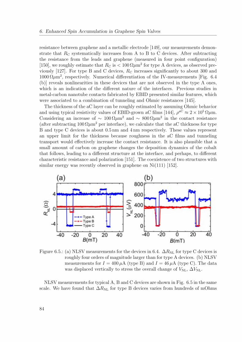
6. Enhanced Spin Accumulation in Graphene Spin Valves
resistance between graphene and a metallic electrode [149], our measurements demon-strate that RC systematically increases from A to B to C devices. After subtractingthe resistance from the leads and graphene (measured in four point configuration)[150], we roughly estimate that RC is < 100 Ωµm2 for type A devices, as observed pre-viously [127]. For type B and C devices, RC increases significantly to about 300 and1000 Ωµm2, respectively. Numerical differentiation of the IV-measurements [Fig. 6.4(b)] reveals nonlinearities in these devices that are not observed in the type A ones,which is an indication of the different nature of the interfaces. Previous studies inmetal-carbon nanotube contacts fabricated by EBID presented similar features, whichwere associated to a combination of tunneling and Ohmic resistances [145].
The thickness of the aC layer can be roughly estimated by assuming Ohmic behaviorand using typical resistivity values of EBID-grown aC films [144], ρaC ≈ 2× 10⁵ Ωµm.Considering an increase of ∼ 100 Ωµm2 and ∼ 800 Ωµm2 in the contact resistance(after subtracting 100 Ωµm2 per interface), we calculate that the aC thickness for typeB and type C devices is about 0.5 nm and 4 nm respectively. These values representan upper limit for the thickness because roughness in the aC films and tunnelingtransport would effectively increase the contact resistance. It is also plausible that asmall amount of carbon on graphene changes the deposition dynamics of the cobaltthat follows, leading to a different structure at the interface, and perhaps, to differentcharacteristic resistance and polarization [151]. The coexistence of two structures withsimilar energy was recently observed in graphene on Ni(111) [152].
Figure 6.5.: (a) NLSV measurements for the devices in 6.4. ∆RNL for type C devices isroughly four orders of magnitude larger than for type A devices. (b) NLSVmeasurements for I = 400µA (type B) and I = 46µA (type C). The datawas displaced vertically to stress the overall change of VNL, ∆VNL.
NLSV measurements for typical A, B and C devices are shown in Fig. 6.5 in the samescale. We have found that ∆RNL for type B devices varies from hundreds of mOhms
84

6.4. Experimental Results and Discussion
to the lower Ohms range, which is three orders of magnitude larger than the values forour type A devices. The enhancement is so large that the features of the measurementsshown in Fig. 6.3 (b) cannot be resolved in Fig. 6.5 (a) and appear as a straight line.For type C devices, ∆RNL is even larger, typically about ten Ohms (≈ 8 Ohms forthe device in Fig. 6.5). This represents an additional order of magnitude increaseand, therefore, up to a 104-fold overall enhancement when comparing with type Adevices. ∆RNL in type B and C devices compares well with the reported values forpinhole contacts using conventional insulators such as MgO or Al2O3 [55, 115, 135]. Asopposed to the case of MgO or Al2O3 interfaces, high-current densities can be appliedto our contacts without deteriorating them. As shown in Fig. 6.5 (b), we are able toachieve very large absolute nonlocal spin voltages of about 500µV, which surpassesthe largest value previously reported in any material by more than a factor 2 [94, 153].In more recent measurements, presented in chapter 7, we demonstrate even highervalues of ∆VNL close to 1 mV. Taking into account the polarization P of the current,this corresponds to a difference in electrochemical potential of spin up and spin downcarriers of 20 meV.
We performed Hanle spin precession measurements to determine the spin relaxationlength λsf of these devices. Such measurements, shown in Fig. 6.6 were only possiblefor type B and C devices because of the small signal and the large spin absorptionby the contacts occurring for the type A ones. By fitting the measurements to a one-dimensional model [8, 55], we obtain λsf ≈ 1.3µm. The distance between the contactsis thus smaller than λsf and minor changes in λsf cannot change the magnitude of RNL
significantly.The fits in Fig. 6.6 also deliver the spin lifetime τsf . For the presented devices, the
spin lifetime is smaller for device C (85 ps) as for device B (146 ps). However, τsf is inthe 100 to 200 ps range for most devices and we do not find a clear correlation betweenthe spin lifetime and the type of substrate (PMMA or SiO2).
Having extracted these parameters, we can obtain the effective polarization P of theferromagnetic electrodes using Eq. 2.34. P is approx. 5 % for device B and approx.10 % for device C. It is interesting to compare these values to those obtained in deviceswith the conventional interface types. For transparent contacts, polarizations as lowas 1 % have been reported [127], for pinhole contacts 2-18 % [55, 154, 155] and valuesas high as 30 % for tunneling (pinhole-free MgO) barriers [135].
We thus argue that the increase in RC is solely due to EBID. In the case of typeB devices, the aC originates from the hydrocarbons present in the chamber of theelectron-beam lithography system, as previously observed [142, 143, 144, 145]. Theadditional increase in RC for type C devices is associated to the release of carbon-rich molecules from the PMMA layer, which act as precursors and decompose in theelectron-beam irradiated area, resulting in a larger aC-deposition rate than at theresidual chamber pressure [142].
The introduction of disorder in graphene by the electron-beam is unlikely at anacceleration voltage of 30 keV, which is below the knock-on damage threshold of carbon
85

6. Enhanced Spin Accumulation in Graphene Spin Valves
Figure 6.6.: Hanle precession measurements of the overexposed devices in Fig. 6.5:type B (a) and type C (b). In both cases, we extract λsf ≈ 1.3µm.
nanostructures [130, 156]. This agrees with the fact that we found no correlationbetween the carrier mobility of the graphene sheet and the exposure to the e-beamdose, even when graphene is fully exposed. Indeed, graphene on crosslinked PMMAfrequently exhibits higher mobility and lower residual doping than graphene on SiO2.The mobilities of the discussed devices were of about 2000 to 3000 cm2/Vs but in somecases it can exceed 20000 cm2/Vs for fully exposed graphene. Examples are shown inFig. 6.7, where we compare resistivities ρ and mobilities µ of a type B and a type Cdevice.
Despite the fact that no signs of degradation of the graphene sheet are observedafter EBID, if possible, one should perform the EBID step in the contact region only,which leaves the graphene between the contacts completely unaffected. This could berelevant for efficient cleaning of the graphene sheet because, as recently pointed out[130], it might not be possible to easily remove amorphous carbon by current annealingafter EBID.
Finally, an additional step in RNL as a function of B, which is due to the switchingof the outer electrodes, becomes apparent in the NLSV measurements of our type Cdevices [Fig. 6.5; B ∼ 15 mT]. This feature is well-known [126] and, for wide contacts,we argue that is only present when a sufficiently large contact resistance preventsthe spin-absorption effect. In Fig. 6.8, we qualitatively show the variation of theelectrochemical potential µHR,T(x) for spin-up and spin-down electrons for transparent(T) and highly resistive (HR) contacts at the detector electrodes, corresponding totype A and type C devices. If the contact resistance is high [Fig. 6.8 (a)], no contactinduced spin relaxation occurs and, therefore, when the magnetization of the outerdetector switches, VNL changes by ∆VNL ∝ ∆µHR(x = x2). In the case of transparentcontacts [Fig. 6.8 (b)], the effect of the spin absorption by the ferromagnet is two-fold.
86

6.5. Conclusion
Figure 6.7.: Mobilities of (a) type B and (c) type C devices. The overexposure requiredduring fabrication of these devices (as shown in Fig. 6.1 (b)) does not leadto a notable degradation of the graphene, as the extracted mobilities canexceed 20000 cm2/Vs at room temperature.
The overall spin accumulation is smaller and, for wide enough contacts, it is completelysuppressed below the contact. In this situation, the switching of the outer detectorelectrode does not affect the measurements because ∆VNL ∝ ∆µT(x = x2) = 0. Ananalogous argument can be made in relation to the second injector. Thus, the fact thatthis feature occurs most notably for type C devices further corroborates our hypothesisof the formation of an aC interface layer that increases the contact resistance betweenCo and graphene and leaves graphene unaffected.
6.5. Conclusion
In summary, we have implemented graphene based non local spin valves on SiO2 andon PMMA. Non local measurements show that an amorphous carbon layer at theFM/graphene interface deposited by electron-beam induced deposition can result ina large enhancement in the spin injection/detection efficiency, even at large appliedinjection currents for which we find the contacts to be stable. Our results show a 104-fold enhancement in comparison to Ohmic contacts, but further improvements can beexpected after optimizing the deposition of carbon by choosing the appropriate car-bon precursor and by controlling its quantity in a suitable electron beam lithographysystem. Nevertheless, further studies are required to precisely determine the nature ofthe interface, which can have Ohmic or tunneling character or a combination of both.
In order to test the transferability of our methods, we have repeated the amor-phous carbon deposition procedure in a second EBL system from a different vendorand have found essentially the same results. This underscore the importance of amor-
87

6. Enhanced Spin Accumulation in Graphene Spin Valves
Figure 6.8.: Schematics of the spin-up and spin-down electrochemical potentials ingraphene for highly resistive (a) and transparent (b) contacts.
phous carbon for future spintronic research, especially because of the simplicity andthe transferabillity of the deposition method and the low reactivity of carbon. Amor-phous carbon can be used as an alternative material to conventional insulators usedin spintronics, such as MgO or Al2O3. In particular, it might open the path for repro-ducible spin transport measurements in carbon allotropes other than graphene, suchas carbon nanotubes, which have eluded researchers for more than a decade.
88

7. Spin Thermocouple and Giant SpinAccumulation in Single LayerGraphene
7.1. Introduction
The interaction between charge, spin and heat currents in solid state media can leadto novel phenomena, which are treated in the field of Spin Caloritronics. We introducethe field, which recently obtained renewed attention, in section 2.7 from a theoreticalpoint of view. Here, we present experimental results underlining the potential ofgraphene for spin caloritronics. In particular, we demonstrate how spin up and spindown carriers in graphene non local spin valves form the two arms of a thermocouple.We therefore refer to this device as a spin thermocouple. Graphene, with its energydependent density of states and Seebeck coefficient S, has the properties required forthe experimental realization of such a device.
In our devices, we observe values of the spin accumulation VNL as large as 1 mV. Thiscorresponds to a spin splitting of approx. 20 meV, which to our knowledge is the largestvalue observed to date in any material. Because of the large splitting, it is possible toobserve considerable quantities of carriers with opposite spin and charge at the Diracpoint, where the spin up carriers are electrons and the spin down carriers holes. Thenon local voltage detected in such a device is therefore significantly enhanced closeto the charge neutrality point when a sizeable Joule heating is present. This is dueto the spin polarization of the heat current caused by the energy dependent Seebeckcoefficient of graphene leading to a supralinear behavior of the spin accumulation VNL
as a function of the bias current.Our observations hint at the possibility of a novel way to control and sustain spin
transport.
7.2. General Concept
7.2.1. Context
The interaction of heat currents and the electronic spin has been a topic of researchsince the 1980s [157]. In recent years, new spin dependent thermal effects have been
89

7. Spin Thermocouple and Giant Spin Accumulation in Single Layer Graphene
discovered in ferromagnets and the topic is receiving renewed interest [23, 24, 25, 45,158]. One of the most intriguing phenomena is the spin Seebeck effect (SSE) in whicha thermal gradient in a ferromagnet gives rise to spin currents that are detected via theinverse spin Hall effect in a metallic strip transverse to the temperature gradient [23].However, even though the SSE is experimentally established in metals, insulators andsemiconductors, the underlying mechanism has been proven far more complex thanoriginally envisioned, involving both magnons and phonons in the ferromagnet andthe substrate.
Figure 7.1.: Charge and spin thermocouple in graphene. (a) Charge thermocoupleformed by two graphene flakes. A thermoelectric voltage is built up dueto the temperature gradient ∇T . The sign of the voltage is determinedby the character of the carriers. (b) Spin thermocouple. If carriers withopposite spin orientation can be approximately described as belonging totwo independent transport channels, the thermolelectric effect in (a) leadsto an anomalous increase of the spin accumulation due to the effective spindependence of the Seebeck coefficient S of graphene.
In this chapter, we describe a new phenomenom in which spin accumulation ingraphene under a thermal gradient presents an anomalous enhancement away fromthe injection point. The spin accumulation is generated by electrical spin injection ina graphene NLSV and the enhancement is due to an effective spin dependent Seebeckcoefficient S.
This can be understood by examining the working principle of a conventional, chargethermocouple. In graphene, such a device can be fabricated using two strips of dis-similar carrier density. In Fig. 7.1 (a), an ideal device is shown in which the majority
90

7.2. General Concept
of carriers in one arm are electrons and in the other arm holes. A thermoelectricvoltage builds up in both arms due to the Seebeck effect, introduced in section 2.2.The sign of the Seebeck coefficient S changes across the charge neutrality point as themajority carriers switch from electrons to holes. If the Fermi levels of the sheets inFig. 7.1 (a) are tuned to be equidistant from the Dirac point, the induced voltage inthe thermocouple is V = 2S∗∆T , where S∗ = |Se| = |Sh| is equal to the magnitude ofthe electron and the hole Seebeck coefficients, Se and Sh respectively, and ∆T is thetemperature difference between the electrodes.
For length scales smaller than the spin relaxation length, carriers with oppositespin orientation in a non magnetic material can be approximately described by twoindependent transport channels. as schematically shown in Fig. 7.1 (b). This isthe two-current model, introduced in section 2.3. In graphene, the spin relaxationlength can exceed several micrometers [115] and spin injection from a FM can resultin very large spin splitting [55, 159]. If the carriers of spin up and spin down subbands have electron or hole character, repectively, the scenario represented in Fig. 7.1(a) is intrinsically present in a single graphene sheet, where electron and holes areconstrained to different spin sub bands instead of the two graphene sheets that formthe thermocouple junction in Fig. 7.1 (a). Because of the symmetry of electrons andholes, the overall thermoelectric voltage between hot and cold ends of the graphenecancels out. However, the spin accumulation µS increases by ∆µS = e∆S∆T c, where∆S = S↑ − S↓ is the difference between the Seebeck coefficients for spin up and spindown, S↑ and S↓, and T c is the effective temperature of the carriers that, in general,can differ from the lattice temperature T l.
7.2.2. Graphene NLSV as Spin Thermocouple
A spin thermocouple, as described above, is formed at the Dirac point of any con-ventional graphene NLSV, if the injector current is large enough to create a sizeableJoule heating. A graphical representation of the device layout is shown in Fig. 7.2:Spin accumulation is generated by electrical spin injection, as the charge current den-sity jc results in a spin current density js in the graphene. For sufficiently large biascurrents I, Joule heating of the injector circuit leads to a temperature gradient ∇Tin the graphene and the substrate. The resulting heat current in the graphene sheetcontributes to the spin accumulation due to the effective spin dependence of S.
Graphene is an ideal candidate to investigate the interplay between spin and heatcurrent related effects. ∆VNL = V ↑ − V ↓, which is the difference of the non localvoltage between the P and AP alignment of the FMs V ↑ and V ↓, is a measure ofthe spin accumulation, while the thermoelectric voltage in the device is given byVth = (V ↑ + V ↓)/2. We further discuss this point in appendix B.2. Vth correspondsto a heat current density jq, which is proportional to the conductivity of graphene,while the spin signal ∆RNL is proportional to σ−1. Tuning the conductivity σ(VBG)therefore constitutes a tool to investigate the relation between spin and heat currents
91

7. Spin Thermocouple and Giant Spin Accumulation in Single Layer Graphene
in graphene NLSV.
Our study is further facilitated by the fact that in case of our graphene NLSV, thespin signal ∆RNL is of the order of a few Ohms, while our interfaces allow for highcurrent densities [159], as discussed in chapter 6.
Figure 7.2.: Schematical representation of a graphene non local spin valve. Four Coelectrodes (yellow) on top of a single layer graphene sheet (magenta).Electrical connections for NLSV measurements are indicated, the relativemagnetization can be switched by the application of an in-plane, exter-nal magnetic field (not shown). The charge current density jc via theCo/graphene interface results in a pure spin current js in the graphene.Additionally, a temperature gradient ∇T builds up, leading to a heat cur-rent jq in the graphene, which can be non negligible when a sizeable Jouleheating is generated. Since the Seebeck coefficient of graphene is spindependent, the heat current is spin polarized as well.
Traditionally, non local spin voltages in NLSVs have been attributed to spin accu-mulation due to pure spin currents in the non magnetic material. These have beenstudied extensively over the last decade [11, 15, 16, 44] and can be understood withinthe widely accepted phenomenological model of non local spin injection [41], whichwe discuss in detail in section 2.5. Pure spin currents are often quantified in termsof the transresistance ∆RNL = ∆VNL/I. In graphene NLSV with highly resistivecontacts, ∆RNL can be expressed as [55] ∆RNL = (P 2
Jλsf/σW ) exp(−L/λsf). Here,PJ is the interfacial current polarization, λsf the spin relaxation length of graphene,σ its conductivity, W the width of the flake and L center to center distance of theelectrodes.
In contrast to the spin current, the heat current is due to Joule heating associatedwith the bias current I and thus proportional to RiI
2, where Ri is the resistance ofthe injector circuit. Joule heating in graphene-metal contacts has been quantified in arecent study [160]. It creates a temperature gradient along graphene, which leads tothe diffusion of hot charge carriers into colder regions of the conductor. As we showin section 2.7, this temperature gradient acts as a generalized force which drives thethermal transport of carriers. Due to the effective spin dependent Seebeck coefficient
92

7.3. Experimental Results
in graphene, also jq contributes to the spin accumulation.
In order to quantify the thermoelectric effects, we calculate the temperature distri-bution in our devices numerically. We find that the temperature difference betweenthe detectors, ∆TDD′ , depends quadratically on the bias current I. The results aresummarized in section B.
Focussing on the bias dependence of our devices, we observe an anomalous enhace-ment of VNL, corresponding to a supralinear behavior of the electrochemical potentialsof spin up and spin down carriers in graphene. This is opposed to the sublinear de-pendence which can be expected by the monotonous increase in the carrier densityaway from the Dirac point.
7.3. Experimental Results
7.3.1. Device Characteristics
In the following, we present data on a particular, representative sample. The fabri-cation of our devices is described in section 3.4.4. We perform non local spin valvemeasurements as described in section 5.3 and chapter 6.
Figure 7.3 (a) shows a scanning electron microscope image of the device. It consistsof four Co electrodes (yellow) in contact with single layer graphene (blue). The width ofthe inner two FMs is 100 nm and 200 nm, respectively, while the width W of grapheneis approx. 900 nm.
A typical NLSV measurement is shown in Fig. 7.3 (b). The switching of the relativemagnetizations of the FM electrodes is reflected in the non local voltage VNL. In termsof transresistance, ∆RNL ≈ 7 Ω. The measurement is carried out at room temperature,with a current of I = 50µA and a backgate voltage of VBG − VD = +3 V.
We measure the field effect of graphene in four point configuration. Applying thebias current I (typically I = 1µA) to the outer electrodes, we measure the voltagedrop between the inner two contacts in order to obtain the four point resistivity ρ4Pof the device. Comparing ρ4P with RNL, as shown in Fig. 7.3 (c), it becomes obviousthat RNL exhibits a peak at the Dirac point, hinting to a tunneling-like behavior ofthe injected carriers [135]. Moreover, we extract the mobility of the sample fromρ4P, which can be as high as 20 000 cm−2, while the residual carrier concentrationni ≈ 1.5 · 1011 cm−2.
The Seebeck coefficient S can be calculated from ρ4P using the semiclassical Mottrelation [27, 161, 162]. This is shown in Fig. 7.3 (d) for room temperature and77 K measurements. The magnitude of S is nominally linear in temperature T from10 K to 300 K [27, 162]. For temperatures above ∼ 200 K however, SMott is known tooverestimate the actual value of S.
Finally, we have determined the spin relaxation length of the device by performingHanle measurements and fitting these to a 1D-model [44]. We obtain values of λsf ≈
93

7. Spin Thermocouple and Giant Spin Accumulation in Single Layer Graphene
Figure 7.3.: Characteristics of sample Q1 (a) SEM image of the device. The scale barequals 1µm. Graphene is exfoliated on a PMMA substrate and four Coelectrodes are deposited on top (b) NLSV measurement for I = 50µA,∆RNL ≈ 7 Ω (c) Four point resistivity ρ4P (left vertical axis) and tran-sresistance ∆RNL for I = 10µA (right vertical axis) as function of VBG.The grey area represents the residual carrier concentration of the device.(d) Seebeck coefficient S at room temperature and 77 K according to theMott formula
1.2µm at the Dirac point, while for other backgate voltages, λsf can be as high as2µm, as shown in Fig. 7.4. With this, we are able to extract the interfacial currentpolarization PJ , finding that PJ ≈ 5 %.
7.3.2. Non Local IV Measurements
We present the main results throughout the following section. Studying the bias de-pendence of our devices, we observe a supralinear dependence of the electrochemicalpotentials of the spin sub bands on the applied bias current I. Moreover, we demon-strate that close to the Dirac point, the carriers in the spin up band are electrons, whilethe spin down carriers are holes, which corresponds to the idealized spin thermocoupledescribed in section 7.2.
94

7.3. Experimental Results
Figure 7.4.: (a) Hanle spin precession in the anti parallel alignment of the FMs fordifferent backgate voltages (b) Fitting the curves in (a) to a two dimen-sional model delivers λsf , which shows a minimum at the Dirac point ofgraphene of λsf ≈ 1.2µm.
The experimental data is shown in Fig. 7.5. It consists of the non local voltage VNL
as function of the bias current for P and AP alignment of the FMs for three differentbackgate voltages. These voltages correspond to the Dirac point of graphene as wellas one point above and one below it, VBG − VD = 0,±4 V. The dashed line indicatesthe mean non local voltage Vth, which exhibits a parabolic behavior as a function ofthe current, as expected of a thermoelectric voltage.
We perform the measurements as follows: First, we prepare the P or AP configura-tion of the injector/detetector FMs in a NLSV measurement by exploiting the memoryeffect of our devices [94], then we sweep the magnetic field back to zero. Second, inthese two states we subsequently measure the non local voltage VNL as a function ofthe injected current. In principle, this constitutes a conventional IV measurement,but in the non local configuration shown in Fig. 7.2. We therefore refer to thistechnique as non local IV (NLIV) measurements. Finally, we repeat the NLIVs fordifferent voltages applied to the backgate, thus varying the carrier concentration, thetype of carriers and the conductivity of graphene. We have confirmed the validity ofour approach by performing several single NLSV measurements for varying currentsand gate voltages.
The NLIVs shown in 7.5 (a) are measured at a backgate voltage of VBG−VD = −4 V.The splitting between VP and VAP increases with the bias current, as the splitting ofspin up and down band increases. The backgate voltage VBG shifts the position ofthe Fermi energy EF relative to the charge neutrality point. The density of states forboth spin sub bands is schematically shown by the Dirac cones in the inset. Here, thecarriers in both spin sub bands are holes and the sign of the parabolic coefficient ofthe NLIVs is negative for both relative alignments of the FMs.
Close to the Dirac point of graphene, as shown in Fig. 7.5 (b), the Fermi level of thespin up band lies above the Dirac point, while the Fermi level of the spin down band lies
95

7. Spin Thermocouple and Giant Spin Accumulation in Single Layer Graphene
below it. Therefore, the carriers in the spin up band are electrons, while the carriers inthe spin down band are holes. The detected non local voltages for P and AP alignmentof the FMs VP and VAP have different signs and parabolic coefficients for each case. The
Figure 7.5.: Non local voltage VNL for dif-ferent gate voltages as func-tion of the bias. The carri-ers in the spin sub bands are(a) holes (b) electrons for spinup, holes for spin down (c)electrons.
thermoelectric voltage Vth is close to zero,as the sign of the carriers is opposite forthe P and AP alignment and both con-tributions cancel each other out, in agree-ment with our expectations.
In Fig. 7.5 (c), the voltage ap-plied to the backgate is VBG − VD =+4 V, meaning that the carriers inboth sub bands are electrons and thesign of the parabolic coefficient is posi-tive.
It becomes clear that the device corre-sponds to the spin thermocouple we de-scribe in section 7.2. At the Dirac point,spin up and spin down currents consist ofopposite type of carriers. Consequently,the thermal enhancement of µS is largestclose to the Dirac point. Moreover, a cor-relation between the type of carrier andthe type of spin exists in this situation,which is not only intriguing from a physicspoint of view, but also important for pos-sible spin caloritronical applications.
To further investigate this point, westudy ∆VNL and ∆RNL as a function ofthe bias current, as shown in Fig. 7.6.The largest spin accumulation is detectedat the Dirac point, VBG = VD, with abso-lute values of VNL close to 1 mV for a biascurrent of 100µA. Taking into account theinterfacial current polarization of approx.5 %, in terms of electrochemical poten-tials this corresponds to µs = 20 meV. Inall three cases, ∆VNL shows a supralinearbehavior as a function of the current, asshown in Fig. 7.6 (a). This is especially
remarkable, because ∆VNL typically decays for increasing bias currents [94]. Here, itincreases due to the thermal enhancement of the signal, which gains weight as the
96

7.3. Experimental Results
bias, and thus the temperature gradient along the sample, increases.At the Dirac Point, ∆RNL is close to 5 Ω at low currents, but increases up to ∼ 10 Ω
at I = 100µA, as shown in Fig. 7.6 (b). It can also be seen that ∆RNL has roughly thesame dependence on the bias current I, if the carriers in the two spin sub bands areeither both electrons or holes, for VBG−VD = ±4 V. ∆RNL increases almost linearly forcurrents above approx. 50µA, and d∆RNL/dI ≈ 10 mV/mA2 for VBG − VD = ±4 V.At the Dirac point, d∆RNL/dI ≈ 25 mV/mA2.
Figure 7.6.: The spin signal ∆RNL for the curves presented in Fig. 7.5. The transre-sistance increases with increasing bias in all cases. The highest values of∆RNL are reached at the Dirac point of graphene.
An increase in RNL with increasing bias is a feature which cannot be explainedwithin the phenomenological model of spin injection. In systems using transparentcontact, ∆RNL is independent of the bias current, according to eq. 2.32. Also insystems using tunneling barriers, ∆RNL is independent of the current, as given by eq.2.34. However, these equations are only valid in the low current regime, as a biasdependence is not considered within the model.
Experimentally, a decrease is observed in most systems [94]. Moreover, as we dis-cuss in detail in chapter 4, the spin polarization in magnetic tunnel junctions quicklydeteriorates as a function of the bias current. As shown there, this is due to intrin-sic properties of the tunneling process of the carriers, therefore limiting the highestabsolute values of VNL.
Additionally, in graphene, due to monotonous increase in the density of states awayfrom the Dirac point, a decaying spin signal RNL can be expected, regardless of thetype of contact.
Nevertheless, examples of linear or even supralinear behavior of the spin signal asa function of the bias can be found in the literature. In transparent contact graphenespin valves, Shiraishi et al. have reported a linear relationship between non localvoltage and bias current, which holds up to I = 1 mA [147]. Again in transparentcontact devices, Han et al. report on an electron hole asymmetry of spin injection,
97

7. Spin Thermocouple and Giant Spin Accumulation in Single Layer Graphene
observing a supralinear increase when the carriers in their devices are holes [163]. Inthat case, ∆RNL increases for a factor 1.25 from ∼ 40 mΩ at currents close to zero to∼ 50 mΩ at I = 200µA. In our case, the increase at the Dirac point is close to a factortwo for currents between 0 and 100µA.
7.3.3. Analysis of the Data
The Polynomial model
In order to investigate the response of our devices to varying types of carriers andconductivities, we have measured several NLIVs, such as the ones shown in Fig. 7.5for different backgate voltages. We analyze the data with a polynomial model, whichallows for a better understanding of the different contributions to the spin signal. Ina first approach, the pure spin current is a first order and the heat current a secondorder effect in respect to the bias current.
We describe the NLIVs for P and AP configuration by
VNL = V0 + rNLI + ΣIγ (7.1)
For γ = 2, this corresponds to a simple polynomial model up to the second order,which is in good agreement with the data (χ2 ≥ 99 %). A previous study has focusedon the role of the second order parameter [164]. However, a recent result [165] suggeststhat a complete analysis of the process requires values of γ deviating from 2.
The parameters of the different orders within eq. 7.1 are spin dependent. Forinstance in case of P alignment of the FM, the equation reads V ↑NL = V ↑0 +r↑NLI+Σ↑Iγ.We further consider ∆VNL = V ↑−V ↓, which is the conventional definition of ∆VNL, andVNL = (V ↑+V ↓)/2. These definitions are equal for all parameters, e.g. Σ = (Σ↑+Σ↓)/2and so on.
The contribution to the spin signal of the different orders of eq. 7.1 can be under-stood as follows:
• The parameter V0 is a constant offset, which is typically of the order of 1µV andwhich we neglect in the following.
• The first order parameter rNL corresponds to the conventional definition of thetransresistance, if V0 = Σ = 0. This means that in the absence of an offsetvoltage V0 and higher order effects, ∆rNL = ∆RNL.
• The higher order contribution ΣIγ can be understood in the following way. Con-sider heat transport in a non magnetic system, where no spin current and no lin-ear contribution to the non local signal is present, rNL = 0. However, due to Jouleheating of the injector contact, a Seebeck voltage can be measured at the detec-tor, which is given by VNL = VSeebeck = −S∆T c, if the Seebeck coefficient S is not
98

7.3. Experimental Results
Figure 7.7.: Results of our analysis (a) First order fitting parameter rNL for P and APalignment as a function of VBG at room temperature (b) Second order fit-ting parameter Σ corresponding to the analysis in a) (c) First order fittingparameter rNL as a function of VBG at 77 K (d) Second order parameterΣ at 77 K
or only weakly temperature dependent. It follows that ΣI2 = VNL = −S∆T c.This is the classical relation 2.3 of the Seebeck effect. Here, γ = 2 and Σ ∝ S.
Now we consider a current consisting of spin up and spin down particles. Withinthe two-current model, this means that V ↑,↓ = −S↑,↓∆T c. Therefore, if S↑ 6= S↓,the higher order contribution of the non local voltage is spin polarized. It canbe expressed as ∆ΣIγ = −(S↑−S↓)∆T c, which is the general expression for theanomalous enhancement of the spin signal as introduced in section 7.2.
The power of I, γ, is therefore determined by two different contributions, ∆S =(S↑ − S↓) and ∆T c.
Close to the Dirac point, the Seebeck coefficient is linear with respect to thebackgate voltage. It follows that also the the contribution to the spin signal dueto ∆S = (S↑ − S↓) is linear with respect to the current, ∆S ∝ I.
The relation between current and temperature also contributes to ΣIγ. Theclassical, well known relation is Joule heating, where ∆T ∝ I2. However, ina recent work, Betz et al. find a linear relation between current and carriertemperature at low bias, T c ∝ I, and T c ∝ I1/2 otherwise, due to the presence
99
7. Spin Thermocouple and Giant Spin Accumulation in Single Layer Graphene
of hot carriers induced by the bias [165].
Taking into account all contributions, it becomes clear that 1.5 ≤ γ ≤ 3. Wefind that the data is well described by γ = 2 in eq. 7.1 in all cases, thus favoringT c ∝ I.
In short, rNL ∼ RNL, while Σ ∼ S. Therefore, Σ shows a Seebeck-type behavior asa function of the backgate, and ∆Σ is proportional to the derivative of the Seebeckcoefficient, as ∆S ∝ dS/dVBG.
Results of the Analysis
Figure 7.7 shows the results of the analysis of data obtained at room temperature aswell as at 77 K.
The first order contribution as a function of backgate voltage VBG gives an indi-cation that the carriers injected into graphene have tunneling like properties, since∆rNL, shown in Fig. 7.7 (a), exhibits a peak at the Dirac point of graphene. For theconventional spin signal ∆RNL this is expected if the device has highly resistive con-tacts, where ∆RNL ∝ R4P [135]. One can also expect that at low injection currents,any higher order effects are negligible, which is the case here. In Fig. 7.3 (b), wecompare ρ4P and ∆RNL, where ∆RNL is measured using a DC current of 10µA. Atcurrents as low as a few µA, ∆RNL ≈ ∆rNL.
Also at low temperatures, ∆rNL exhibits a peak at the Dirac point of graphene, asshown in Fig. 7.7 (c).
The second order parameters Σ↑,↓ at room temperature are shown as a functionof the backgate voltage VBG in Fig. 7.7 (b). The dashed line indicates Σ = (Σ↑ +Σ↓)/2, which is in qualitative agreement with the Seebeck coefficient of graphene,as shown in Fig. 7.8. Rescaling Σ by using the relation between bias current andtemperature difference obtained by the numerical simulation, we can convert Σ↑,↓ tothe spin dependent Seebeck coefficients of graphene S↑,↓. This is demonstrated indetail in appendix B.4.
While Σ is proportional to S, the anomalous enhancement of the spin accumulationis proportional to ∆Σ and thus ∆S. In fact, ∆Σ as given by the polynomial modelcorresponds to the derivative of ∆RNL with respect to the current I. This follows fromthe definition of the model, where ∆RNL = ∆rNL + ∆Σ · I and thus d∆RNL/dI = ∆Σ.We can therefore obtain ∆Σ by fitting the NLIVs with the polynomial model, or bynumerically differentiating ∆RNL(I), as in section 7.3.2.
Since d∆RNL/dI is constant over a considerable range of currents, the differencebetween the two methods is negligible and the values extracted from the curves shownin Fig. 7.6 (b) correspond well with the values of ∆Σ obtained from the fitting, asshown in Fig. 7.7.
At 77 K, as shown in Fig. 7.7 (d), the values of Σ↑,↓ and ∆Σ are smaller thanat room temperature. This is due to the fact that many material parameters of the
100

7.3. Experimental Results
system, such as the thermal conductivity or specific heat of graphene are smaller thanat room temperature [28]. Especially, S(77 K) < S(300 K), as shown in Fig. 7.3 (d),and thus also Σ and ∆Σ are smaller than at room temperature.
Figure 7.8.: (a) Seebeck coefficient of the device according to the Mott formula incomparision with the second order parameter Σ (b) Both −dS/dVBG aswell as ∆Σ exhibit a peak around the Dirac point of graphene
A comparision between SMott and Σ is shown in Fig. 7.8 (a). In fact, they exhibit thesame behavior as a function of the backgate voltage VBG. This can be used in orderto obtain a conversion factor between Seebeck coefficient and second order fittingparameter. Here, we obtain 1 mV/mA2 ≈ 5µV/K.
In Fig. 7.8 (b), a comparision between −dS/dVBG and ∆Σ is shown. Again, thecurves exhibit qualitative agreement. Moreover, the reason for the peak in ∆Σ aroundthe Dirac point becomes clear. As noted above, within the polynomial model, ∆Σ =d∆RNL/dVBG, meaning that ∆Σ is a measure of the variation of ∆RNL with the biascurrent. Since −dS/dVBG has a peak around the Dirac point, this implies that at VD,the strongest enhancement of the non local signal with the bias can be found.
Altogether, our analysis demonstrates that due to the spin dependency of the secondorder parameter Σ, we observe the anomalous enhancement of the non local voltage,which is most pronounced at the Dirac point of graphene.
7.3.4. Hot Carriers
While the analysis of the NLIVs based on the polynomial model delivers a qualitativedescription of our observations, a discrepancy becomes apparent when trying to obtainquantitative results.
The enhancement of the non local signal can be expressed as ∆µS = e∆S∆T . Whilewe obtain ∆µS and ∆S experimentally, we extract ∆T from the numerical calulationof the temperature profile of the sample. However, the numerical simulation deliversthe temperature of the lattice, which can differ from that of the carriers.
101

7. Spin Thermocouple and Giant Spin Accumulation in Single Layer Graphene
At room temperature, it becomes obvious that the lattice temperature is at leastone order of magnitude lower than the temperature required by ∆µS = e∆S∆T .At lower temperatures such as 77 K, the discrepancy is even more pronounced. Wefind that values of ∆T of several hundred Kelvin would be required, implying devicetemperatures of several thousands of Kelvin.
Figure 7.9.: Schematical representation of the physics of hot electrons (a) Schematicrepresentation of the Fermi levels of graphene close to the point of injectionand close to the point of detection. (b) Schematic representation of thedevice and the decay of hot carriers in graphene. At room temperature,the injected, highly energetic carriers quickly thermalize with the lattice,while at 77 K, they reach the two detectors.
We conclude that the numerical model underestimates the temperature of the carri-ers T c, which might be higher than the temperature of the lattice T l. This conclusionis in agreement with a recent study, where electronic temperatures T e of up to 1200 Kin graphene have been reported [166]. In the following, we simply refer to these carri-ers, whose energy is considerably higher than that of the lattice, as hot carriers. Theythermalize with the lattice via scattering processes, most importantly via disorderassisted scattering, which has been studied in graphene recently [167].
The existence of hot carriers at the point of detection can be explained by thelow density of impurities of our devices and the large electric fields. As carriers areaccelerated, they gain kinetic energy, which they loose by inelastic scattering withphonons. Because intrinsic optical phonons, which interact strongly with carriers,have an energy ∼200 meV, the relaxation for lower energies is slow. Therefore, thecarriers arrive at the detector with an energy exceeding the thermal energy for anamount proportional to the temperature of the carriers, E ∝ T c, as schematicallyshown in Fig. 7.9 (a).
102

7.4. Conclusion
In Fig. 7.9 (b), a sketch of the sample is shown together with a simulation of themean free path λe of the hot carriers as a function of the lateral distance from thepoint of injection, based on Ref. [167]. The carriers are injected into graphene atx = 0, while the non local voltage VNL is detected between the detectors D and D′.For our analysis, we therefore have to take into account the temperature difference∆TDD′ between the two detectors as well as ∆TID between injector and first detector,and depending on the situation, we have to choose between ∆TID and ∆TDD′ .
For instance, when comparing Vth and S, it is valid that −Vth/∆TDD′ = S, since Vthis detected between D and D′. On the other hand, the higher order contribution tothe spin signal is given by the spin dependent S the carriers experience while travelingfrom injector I to first detector D. This means that ∆µS = e∆S∆TID.
As shown by Song et al. [167], the lifetime of hot carriers decreases as the tempera-ture increases, since they thermalize via disorder assisted scattering events. Therefore,at room temperature, ∆TDD′ ≈ ∆T lattice
DD′ . This is supported by the fact that using∆TDD′ obtained by the numerical calculation, which delivers the temperature of thelattice, in −Vth/TDD′ = S results in a Seebeck coefficient of graphene which is in goodagreement with the values reported in the literature [27, 162].
However, even at room temperature ∆TID 6= ∆T latticeID . Therefore, when trying to
quantify our results via ∆2µ = e∆S∆T , as shown above, we observe a discrepancy ofone order of magnitude.
The discrepancy is even larger at low temperatures such as 77 K. As schematicallyshown in Fig. 7.9 (b), at 77 K also ∆TDD′ 6= ∆T lattice
DD′ , which has to be taken intoaccount when analyzing the data.
Apart from the quantitative discrepancies, a strong indication for the presence ofhot carriers in our experiments can be found in the analysis of the data, namely in Fig.7.7 (c). As pointed out, at low temperatures there is a linear relationship betweenT c and I [165]. This means that the Seebeck effect becomes a first order effect withrespect to the current, VSeebeck ∝ I. In fact, the first order contribution to the nonlocal signal at 77 K exhibits a Seebeck like backgate dependence, which is not observedat room temperature.
7.4. Conclusion
In conclusion, we have shown that in graphene the combination of spin currents withits energy dependent mobility and density of states can result in novel phenomenain spin caloritronics. We demonstrate that graphene non local spin valves can act asspin thermocouples, when a sizeable Joule heating is generated. A thermal gradientbetween injector and detector results in large thermoelectric spin voltages. The differ-ence between the electrochemical potential of spin up and spin down electrons reaches20 meV and is of the order of typical electronic density distributions of carriers ingraphene. Therefore, the coexistence of a large quantity of carriers with electron and
103

7. Spin Thermocouple and Giant Spin Accumulation in Single Layer Graphene
hole character with opposite spin polarization becomes possible. This is reflected in ananomalous increase of the non local spin signal at the Dirac point as a function of thecurrent bias. Our observations suggest that the transport of spin information in ultraclean graphene could be sustained by thermal transport over macroscopic distances,where spin signal relaxation is partially compensated by thermal transport.
104

8. Conclusions
The main topic of this thesis is the study of pure spin and heat currents in graphenenon local spin valves via means of electrical spin injection and detection. In a prelim-inary work, we analytically investigate the tunneling process of conduction electronsbetween ferro- and non magnetic materials. On the experimental side, we report onelectrical detection of spin precession in freely suspended graphene spin valves. Inthis context, we have developed a novel method for the fabrication of freely suspendedgraphene devices, which additionally is beneficial for the spin injection/detection ef-ficiency of the devices. In order to investigate these enhanced spin signals, we haveperformed bias dependent measurements, which ultimately lead to the experimentaldemonstration of a spin thermocouple in graphene.
In order to further investigate tunneling of conduction electrons between ferro- andnon magnetic electrodes, we have developed a theoretical model based on the analyticalsolution of the one-dimensional, time-independent Schrodinger equation. Focussingon the bias dependence of the spin polarization, we predict a change in sign of thepolarization when tunneling takes place from FM to NM.
More importantly, the model shows that a complex behavior of the polarization isintrinsic to the tunneling process of electrons.
Due to its low spin orbit coupling, long spin relaxations times of several tens of µm ingraphene have been predicted. A promising approach to study the intrinsic propertiesof graphene is to suspend the flakes, thus eliminating the influence of the substrateand enabling cleaning methods which help removing impurities and contamination.
In order to achieve this, we have developed a method to fabricate freely suspendedgraphene non local spin valves that involves a minimal number of steps and chemicals.It is based on the process of crosslinking the polymer PMMA, which is carried out byoverexposure of the polymer by electron beam radiation. We have carried out extensiveefforts in order to ensure the feasibility of the method, including characterization viaoptical, electron beam and atomic force microscopy.
Since the method is acid free, the yield of high quality, as-processed devices isnotably improved when comparing to the standard fabrication process, which requiresagressive chemicals such as hydrofluoric (HF) acid. However, further improvementsin terms of mobility can be expected by employing post processing cleaning methods.These include annealing in an Hydrogen/Argon environment as well as current-inducedcleaning. Nevertheless, our as-processed devices exhibit excellent mobility, which can
105

8. Conclusions
be as high as 2× 104 cm2V−1s−1 at room temperature.We demonstrate electrical detection of spin preccesion, allowing us to extract the
spin relaxation length in these devices, finding values of a few µm. This is similar tothe values obtained in non suspended devices of lower mobility, in contrast to the the-oretical predictions. Therefore, it seems that these early predictions have overlookedlimiting factors for the spin relaxation length in graphene. To date, no explanationfor the discrepancy has been given.
We expect that by applying cleaning methods to freely suspended spin valves, itwill be possible to obtain ultra high mobility samples, therefore opening the path toinvestigating the origins of spin relaxation in intrinsic graphene.
Moreover, the properties of graphene under the influence of external strain havereceived much attention recently. In this context, freely suspended spin valves arenatural candidates for the investigation of pseudomagnetic fields in strained graphene.While many theoretical studies of this topic are available, experimental data is rela-tively scarce.
Besides studying mechanisms of spin relaxation, we have observed an enhancedspin injection/detection efficiency in our devices. In order to investigate the originsof the enhancement, we have fabricated samples on PMMA and SiO2 substrates. Inboth cases, we observe the enhanced spin accumulation, which we attribute to theformation of an amorphous carbon (aC) layer at the interface between graphene andferromagnet due to electron beam induced deposition. Because of the low atomicweight of carbon, the dephasing of spins in the barrier is low, making aC an excellentchoice for applications in spintronics.
The interfaces are stable even for large applied bias current densities. We obtaina 104 enhancement of the spin signal as compared to Ohmic contacts, but expectfurther increase after optimizing the depostion method. While the IV characteristicsof the devices are almost linear, the increased contact resistance and spin accumulationsuggests that the interface could be a combination of Ohmic and tunneling properties.
The simplicity and transferability of the fabrication process is in contrast to those ofAl2O3 or MgO tunneling barriers, which are the conventional insulators used in spin-tronics. Therefore, we expect that aC barriers are a viable alternative, which mightnot only improve the spin injection/detection in non local spin valves in graphene, butin other materials as well.
Finally, we have performed bias dependent measurements in our samples, observinga novel phenonenom which is due to the particular properties of graphene such asits energy dependent mobility and density of states. We demonstrate an anomalousenhancement of the spin accumulation at the Dirac point, which is caused by Jouleheating in the injector contacts and the resulting thermal gradient and thus increaseswith the bias.
Because of this quadratic contribution to the spin accumulation, the electrochemical
106

potentials of the spin sub bands exhibit supralinear behavior as a function of the biascurrent. The spin splitting becomes so large, of the order of 20 meV, that at theDirac point we observe a huge quantity of spin up carriers with electron and spindown carriers with hole caracter, simultaneously. We show that this constitues a spinthermocouple, where the two arms of the device are formed by the different types ofspin in a single graphene sheet and the thermoelectric voltage between spin up andspin down contributes to and thus enhances the total spin accumulation.
107


9. Acknowledgements
As it is good tradition, I would like to acknowledege the help I received from manypersons during the past five years and express my gratitude to everybody.
First of all, I would like to thank my PhD supervisior, Sergio Valenzuela, for provid-ing me with the opportunity to work at the ICN in Barcelona. I especially appreciatethe huge amount of freedom I enjoyed when it came to sample fabrication and con-ducting measurements. Sergio is certainly one of the best physicists I met, so he hasbeen a great guide and at the same time, I always felt it was a great honour for me towrite my PhD thesis in his newly founded group. Beside all these things concerningthe work at the institute, I will not forget the unconditional support I experiencedfrom Sergio when I had a hard time after a bicycle accident, which forced me to takea break from my PhD for several months. Especially this kind of support cannot betaken for granted. Thanks for everything, Sergio!
Then, of course, there are the members of the group I got to know over the years.In the beginning, I learned nearly in the lab everything from Marius Costache, howto make samples and especially how to measure them. I still havent´t met anybodywho measures as thorough as he does. Marius also told me that ‘If you know how tocook, you know how to make samples‘. I really like that sentence, as it contains a reallesson.
German Bridoux was another great colleague, who joined somewhat later and hewas providing heart and soul to the group. He took care of the voluntary work nobodyvolounteers for and generally was helpful in every aspect. Even though he already leftthe group, German has proven extremely helpful in proofreading this thesis.
With Juan Sierra, we started talking Spanish in the group which is quite an achieve-ment. Since he also joined the graphene project, I had many fruitful discussions withhim. As German, Marius and Sergio, he was very helpful in proofreading my thesisand giving me critical comments, especially any time I mentioned GMR.
Finally, I would like to thank Joris Van de Vondel, with whom I started to workon graphene after spending the first year of my PhD with nanowires. Joris is still theundisputed master of the Scotch tape, so thanks a lot for teaching me how to do it.
There have been many colleagues from other groups, whose help I would like toacknowledge. Maria Jose Esplandiu has been very helpful in questions concerningsample fabrication. Moreover, I especially respect her for her unshakable profession-alism amongst the every day chaos of the institute.
109

9. Acknowledgements
From Adrian Bachtold´s group, I owe the biggest thanks to Joel Moser. When Jorisand me started exfoliating graphene, he generously showed us all the little tricks anddetails we needed to know. Johannes Guttinger was very helpful in discussing ourresults and providing me with a Matlab script for the analysis. I would also like tothank Peter Weber, Ioannis Tsioutsios, Marianna Sledzinska and Daniel Garcıa forfruitful discussions regarding sample fabrication and analysis.
From Pietro Gambardella´s group I would like to thank Corneliu Nistor for theHelium, which came just at the right time for me, even though the measurements didnot make it into this thesis. From the group of Clivia Sotomayor Torres, I would liketo thank Francesc Alzina for the help with the Raman measurements, and also forletting us use the nitrogen vessel for such along time. I would also like to thank Cliviaherself, who shared some of her time in order to give me valuable advice regarding thegerman universitarian system. Many Thanks also to Stephan Roche for making sureUI would not miss the Graphene conference in Bilbao in 2013.
As mentioned above, I had started my PhD working with nanowires grown in thegroup of Victor Puntes by Miriam Varon, I would like to express my gratitude for thecollaboration. Miriam also gave me some helpful advice regarding the PhD proceduresat the Autonoma.
Then there are the many employees of the ICN, the UAB and the CNM, who madetheir contribution.
I would like to thank Xavi Ros and Carlos from maintainence, who we could relyon if something in the lab needed fixing, which was quite frequent. In the CNM cleanroom, I had the pleasure of working on the excellent nanolithography system kept inshape by Xevi Borrise, and when he was absent, by Jordi Llobet, who also helped meuse the focused ion beam system. On the occasions I had to use the clean room of theUAB, Maria Angeles Benıtez and Raquel Palencia have been so kind as to give us ahand whenever we needed the facilities.
I would like to thank Belen Ballesteros and Marcos Rosado of the electron mi-croscopy department, who helped in taking TEM or other special images. Wheneverwe needed to contact a workshop, or draw technical designs, or order mechanicalpieces for the laboratory, Gustavo Ceballos was the man with the connections andalso helping with the technical drawings.
Then there were the people in administration. I apologize if I forget somebody,there are just so many. Thanks a lot to Rosa Juan, Anabel Rodrıguez, Marta de laOsa, Sandra Domene, Laura Camarero, Inma Cano, Matias Pueyo, Lluis Bellafontand also Oscar Cardenal, Oliver Fernandez and Manfred Hoeflich from IT.
Last but not least, my special thanks to the former boss of the institute, JordiPascual, who had the talent of giving everybody, even the most miserable of PhDstudents, the feeling of being an important part of the ICN. Moreover, he also acceptedthe responsibility to act as the tutor of my thesis and generally did a great job at theICN. Without him, I doubt the institute would be where it is now.
110

Finally, I would like to thank the members of my PhD committee, Luis Hueso,Xavier Cartoixa, Laurent Vila, Teresa Puig and Stephan Roche for the effort of read-ing my thesis and attending the defence.
Next I would like to acknowledge the help I received from people outside of theuniversity whose support might not have had a direct impact on muy thesis, butwhich was important for me nevertheless. I will just use the language most fitting tothe person from now on.
En primer lugar, quiero dar las gracias a mi esposa, Miriam Jimenez Berruezo.No puedo agradecerte lo suficiente por tu carino, tu comprension y el apoyo que medemuestras todos los dıas.
He tingut molta sort de tenir un amic com el Jordi, qui em va portar a tots els llocsno turıstics de Barcelona, i va fer una gran contribucio en fer-me sentir benvingut aquı.Vaig perdre el compte de quantes vegades hi vam anar a veure el classic juntamentamb al Dani.
Siempre fui bienvenido en la casa de Cris, Manolito y Berta. Manolito fue de laspocas personas que fuera del instituto se interesaba por mi investigacion. Otra parejaque que me recibio a menudo en su casa fueron Loli y Toni, y Toni fue otra personaa quien le gustaba escuchar acerca de mis estudios.
Muchas gracias tambien a Juanjo y Silvi, por su amistad incondicional y su ayudaen momentos duros. Gracias tambien a Anna, Laiki, Ana y Angel, ası como Xavi,Cristina y Michael.
Tambien me gustarıa dar las gracias a la gente de egarsat, especialmente al doctorFallone y Salva, que hicieron un trabajo excelente en ponerme de una pieza otra vez.
Schliesslich mochte ich mich bei meiner Familie fur die nimmermude Unterstutzungbedanken, die ich uber die Jahre immer gespurt habe, und ohne die diese Arbeit nichtmoglich gewesen ware. Vielen Dank an meine Eltern Christa und Henning, an meineSchwester Kristin und an meinen Bruder Helge.
111

A. List of Publications
• Detection of Spin Precession in Freely Suspended Graphene Spin Valves on Cross-Linked Poly(methyl methacrylate)Ingmar Neumann, Joris Van de Vondel, German Bridoux, Marius V. Costache,Francesc Alzina, Clivia M. Sotomayor Torres, and Sergio O. ValenzuelaSmall 9, 156 (2012)
• Enhanced spin accumulation at room temperature in graphene spin valves withamorphous carbon interfacial layersIngmar Neumann, Marius V. Costache, German Bridoux, Juan F. Sierra, andSergio O. ValenzuelaApplied Physics Letters 103, 112401 (2013)
• Spin ThermocoupleIngmar Neumann, Juan F. Sierra, Marius V. Costache, and Sergio O. Valenzuelain preparation
• Enhanced spin signal in nonlocal devices based on a ferromagnetic CoFeAl alloyGerman Bridoux, Marius V. Costache, Joris Van de Vondel, Ingmar Neumann,and Sergio O. ValenzuelaApplied Physics Letters 99, 102107 (2011)
• Magnon-drag thermopileMarius V. Costache, German Bridoux, Ingmar Neumann, and Sergio O. Valen-zuelaNature Materials 11, 199-202 (2012)
• Lateral metallic devices made by a multiangle shadow evaporation techniqueMarius V. Costache, German Bridoux, Ingmar Neumann, and Sergio O. Valen-zuelaJournal of Vacuum Science and Technology B 30, 04E105 (2012)
113

A. List of Publications
• Fingerprints of Inelastic Transport at the Surface of the Topological InsulatorBi2Se3: Role of Electron-Phonon CouplingMarius V. Costache, Ingmar Neumann, Juan F. Sierra, V. Marinova, M. M.Gospodinov, Stephan Roche, and Sergio O. ValenzuelaPhysical Review Letters 112, 086601 (2014)
114

B. Supplementary Material toChapter 7
B.1. Numerical Simulation of the Temperature Profile
In the following, we present results of a numerical simulation of the temperatureprofile of our devices. It is based on a solution of the steady state heat equation intwo dimensions using the numerical calculation software Comsol.
Figure B.1.: (a) Sample geometry used in the numerical calculation of the temperatureprofile, showing the temperature distribution for an injector current of I =100µA (b) Cross section of the temperature profile along the graphenefor a current of I = 100µA, position of detectors indicated by arrows (c)Cross section for I = 50µA
115

B. Supplementary Material to Chapter 7
The geometry of our model is schematically shown in Fig. B.1 (a). It consists of a 2Dcross section of a graphene spin valve perpendicular to the axis of the FMs. Dependingon the type of device, the substrate is either given by 300µm/440 nm of Si/SiO2 or of300µm/285 nm/200 nm of Si/SiO2/PMMA. In the following, we present results of thenumerical simulation of device Q1, which has a Si/SiO2/PMMA substrate. Grapheneis represented as a 1 nm thin layer, while the height of the FMs is 26 nm. The widthof these FMs is, as shown in Fig. B.1 (a), 500/200/100/500 nm from left to right. Theleft two electrodes I and I′ serve as injector circuit, while the right two electrodes Dand D′ are used to measure the non local voltages VNL. The center to center distancebetween I and D is L = 1.15µm, while the distance D to D′ is 2µm.
The source of heat in our model is Joule heating of the injector circuit, consisting ofthe two Co electrodes as well as the graphene in between them. This can be writtenas Pi = RiI
2, where the Ri are the resistances of leads and graphene (i = 1, 2, 3).Dividing Pi by the three dimensional volumes Vi of these elements delivers Qi =Pi/Vi. The external temperature is taken into account by the fact that we demandthe bottom of the substrate to remain fixed at 300 K. Since the thickness of the Silayer is several orders of magnitude larger than those of the dielectric layers, this is anatural assumption.
Figure B.2.: Temperature difference between injector I and detector D, ∆TID, andbetween D and D′, ∆TDD′ as function of the bias current
The resulting heat profile for I = 100µA is shown on a false color scale in Fig.B.1 (a). As shown in the image for a bias current of I = 100µA, only the graphenesheet, SiO2, PMMA and the FMs experience a non negligible deviation from roomtemperature.
Temperature profiles along the center of the graphene sheet are shown in Fig. B.1,for bias currents of I = 100µA in (b) and I = 50µA in (c). The position of thedetectors D and D′ is indicated by arrows and visible as plateaus in the profile. Thesection between injector I and detector D is the range between x = 0, ..., 1.05µm. Fora current of I = 100µA, the temperature close to the device rises to approx. 325 K.
In the following, we turn our attention to the temperature differences between in-
116

B.2. Non Local and Thermoelectric Voltage
jector I and detector D, ∆TID , and between D and D′, ∆TDD′ . In particular, westudy their bias current dependence. Both ∆TID and ∆TDD′ are shown as a functionof the bias current I in Fig. B.2. We obtain these curves by repeatedly performingthe numerical calculation of the entire geometry for varying injector currents, rangingfrom 10 to 100µA. Then, we read out temperature profiles along the graphene, suchas the ones shown in Fig. B.1, in order to obtain ∆TID and ∆TDD′ . Examining theirbias dependence, it becomes clear that both can be described by a parabolic model,delivering a straightforward relationship between ∆T and I. This proves especiallyuseful in the analysis of the NLIVs, as it provides us, for instance, with the possibil-ity of comparing the higher order fitting parameter Σ with the Seebeck coefficient ofgraphene, as shown in section B.4.
Finally, the effect of the hot carriers mentioned in section 7.3.4 is not taken intoaccount by the model, which can only be used to compute the temperature distri-bution of the lattice. At room temperature, these carriers exist only close to theinjector, thus affecting only ∆TID. Therefore, while ∆TDD′ is sufficiently accurate,∆TID underestimates the temperature difference between injector and detector.
B.2. Non Local and Thermoelectric Voltage
The average non local voltage discussed throughout chapter 7 is given by Vth = (V ↑+V ↓)/2. It is the thermoelectric voltage one would detect in a non magnetic system, aswe show in the following.
Figure B.3.: (a) Mean non local voltage −Vth as function of backgate voltage VBG
for different bias currents I (b) -Vth/∆TDD′ matches S qualitatively andquantitatively.
Thermoelectric voltage and Seebeck coefficient of a material are related via eq. 2.3,Vth = −S∆T . Experimentally, often both Vth as well as ∆T are measured in order toobtain S, such as in ref. [27]. Here, we use Vth obtained from averaging the detectednon local voltages in parallel or anti parallel configuration of the FMs, as well as the
117

B. Supplementary Material to Chapter 7
temperature difference ∆TDD′ obtained from the numerical calculation. These deliverthe Seebeck coefficient of graphene via S = −Vth/∆TDD′ , as shown in Fig. B.3.
In Fig. B.3 (a), the non local voltages in device Q1 are shown as a function of thebackgate voltage, for bias currents ranging from 50 to 100µA at room temperature.It can be seen that −Vth qualitatively resembles the Seebeck coefficient of graphene.
Scaling these voltage with ∆TDD′ delivers the Seebeck coefficient of graphene. Asshown in Fig. B.3 (b), the resulting S is nearly independent of the measurementcurrent. Moreover, the maximum of S on the left side of VD equals approx. 100µV/Kand the minimum on the right side of VD equals approx. −50µV/K, similar to thevalues reported in previous studies [27, 162].
These results show that the average non local voltage is indeed identical with thethermoelectric voltage measured in classical and semiclassical physics. In fact, thedetected voltages in ref. [27] or any thermolectric element can be seen as non localvoltage, although historically they are referred to as thermoelectric voltages.
B.3. Temperature obtained via Mott Relation
At lower temperatures such as 77 K, the numerical model described in section B.1does not provide reliable values because of the strong temperature dependence of thematerial parameters. However, we can estimate the temperature difference betweenthe detectors, ∆TDD′ , by comparing Vth and SMott.
Figure B.4.: (a) Thermolelectric voltage Vth for different bias currents scaled by ∆TMottDD′
in order to match SMott (b) Temperature difference ∆TMottDD′ obtainedby scaling between Vth and SMott as function of the bias
As described in chapter 2, the Mott relation delivers a method to calculate theSeebeck coefficient S of graphene from the backgate dependent conductivity σ ofgraphene. Here, we use the mesoscopic form of the Mott relation [161, 27, 162]. Forroom temperature and 77 K, SMott is shown in Fig 7.3 (d).
118

B.4. Spin Dependent Seebeck Coefficients
The relation −Vth/∆TDD′ = S allows us to extract ∆TDD′ . This is shown in Fig. B.4.By matching −Vth and SMott, we can extract ∆TDD′ as scaling factor between them.In Fig. B.4 (a), this is shown for different currents. The resulting ∆TDD′ as functionof the current is shown in Fig. B.4 (b). As in case of the numerical calculation, weobtain a quadratic relation between ∆TDD′ and I.
B.4. Spin Dependent Seebeck Coefficients
Combining the results presented thoughout this appendix with the analysis of theNLIVs of chapter 7, we can gain a better understanding of the involved physics andobtain surprising results.
Figure B.5.: Spin dependent Seebeck parameters S↑ and S↓ obtained from higher orderparameter Σ↑,↓ (a) S and ∆S according to the numerical simulation (b) Sand ∆S according to temperature differences obtained from Mott relation
As explained in chapter 7, we analyze the NLIVs using VNL = V0 + rNLI + ΣIγ,where we set γ = 2. Therefore, Σ is the parameter describing second order effects.As we show in the following, Σ↑,↓ can be identified with the Seebeck coefficients ofspin up and down, S↑,↓. This can be accieved using the relation between ∆TDD′ andI. As discussed in section B.1, the numerical simulation of the temperature profiledelivers a scaling factor of 0.65 mK/µA2 between ∆TDD′ and I. Therefore, Σ and S arerelated via S↑,↓ = −(Σ↑,↓/0.65)10−3 µV/K. The temperature difference obtained fromthe Mott relation, as shown in section B.3, delivers S↑,↓ = −(Σ↑,↓/0.25)10−3 µV/K.
The resulting S↑,↓ are shown in Fig. B.5, together with S = (S↑ + S↓)/2 and∆S = S↑−S↓. In order to stress the similarity between S and Σ as shown in Fig. 7.7,we present the results in terms of −S. The average value S is in good, quantitativeagreement with values found in the literature [27, 162] and with the Seebeck coefficientobtained from the Mott relation, especially S shown in Fig. B.5 (a).
The parameter ∆S is the spin dependent Seebeck coefficient, as defined as SS in aprevious work by Dejene et al. [168], where the authors investigate the spin depen-dent properties of ferromagnetic metals. Here, we study the non magnetic material
119
B. Supplementary Material to Chapter 7
graphene, so it should be valid that S↑ = S↓ and ∆S = 0. However, due to the largespin accumulatiion, we observe a spin imbalance and ∆S 6= 0. This means that weobserve an effective spin dependent Seebeck effect in graphene, which leads to theenhancement of the non local signal and which we describe as spin thermocouple.
Finally, we can extract the effective spin dependent Seebeck coefficient ∆S ofgraphene. It shows a peak around the Dirac point, which is due to the propertiesof graphene. As we show in chapter 7, ∆S ∝ dS/dVBG. The values of ∆S lie in therange of 10 to 40µV/K, which is an order of magnitude larger than the spin dependentSeebeck coefficients of Co or NiFe [168].
120

C. Recipes for the sample fabrication
All devices have been fabricated in a Raith-150Two EBL system at an acceleratingvoltage of 30 keV.
Fabrication of Graphene Devices on a Si-Substrate
1. Patterning of a substrate with markers (5 nm Ti, 20 nm Au). Substrate: p-dopedSi/SiO2m, oxide thickness 440 nm or 285 nm
2. Mechanical exfoliation of graphene (Scotch tape)
3. Localization of graphene
4. Design of contacts
5. Spin-coating:2 layers PMMA 495 A2 at 2500 rpm (40 s), 1.5 min at 180o C 1 layer PMMA 950A2 at 2500 rpm (40 s), 5 min at 180o C
6. EBL contacts: Dose 420µC/cm2
Small features (contacts): Aperture 20µm, stepsize 15 nmLeads: Aperture 120µm, stepsize 15 nmBondpads: Aperture 120µm, stepsize 100 nm
7. Developing: MIBK:Isopropanol (1:3) for 30 s, isopropanol for 90 s
8. E-beam evaporation metal contacts (26 nm of Co), base pressure approx. 1 ·10−7 mTorr, accelerating voltage 8 keV, Current approx. 50 mA
9. Lift-off in acetone and isopropanol
Fabrication of Overexposed Graphene Samples (Type B in 6)
1. Patterning of a substrate with markers (5 nm Ti, 20 nm Au). Substrate: p-dopedSi/440 nm SiO2
2. Mechanical exfoliation
3. Localization of graphene
121

C. Recipes for the sample fabrication
4. Design of contacts
5. Overexposure by e-beam: Dose 9000µC/cm2, Aperture 20µm, stepsize 15 nm
6. Spin-coating:2 layers PMMA 495 A2 at 2500 rpm (40 s), 1.5 min at 180o C1 layer PMMA 950 A2 at 2500 rpm (40 s), 5 min at 180o C
7. EBL contacts: Dose 420µC/cm2:Small features (contacts): Aperture 20µm, stepsize 15 nmLeads: Aperture 120µm, stepsize 15 nmBondpads: Aperture 120µm, stepsize 100 nm
8. Developing: MIBK:Isopropanol
9. E-beam evaporation metal contacts (26 nm of Co)
10. Lift-off
Fabrication of Graphene Spin Valves using PMMA as Substrate (Sus-pended Graphene Spin Valves)
1. Patterning of a substrate with markers (5 nm Ti, 20 nm Au). Substrate: p-dopedSi/285 nm SiO2
2. Spin coating:3 layers PMMA 950 A2 at 2500 rpm (40 s), 1.5 min at 180o C1 layers PMMA 950 A2 at 2500 rpm (40 s), 5 min at 180o C
3. Mechanical exfoliation
4. Localization of graphene
5. Design of contacts
6. Crosslinking of PMMA: Dose 9000µC/cm2, Aperture 20µm, stepsize 15 nmOverexposure of large areas: Aperture 120µm, stepsize 15 nm.Depending on the geometry of the overexposed area, either suspeded devicesresult or those using PMMA as substrate (Type C in chapter 6).
7. Spin-coating:2 layers PMMA 495 A2 at 2500 rpm (40 s), 1.5 min at 180o C1 layer PMMA 950 A2 at 2500 rpm (40 s), 5 min at 180o C
122

8. EBL contacts, dose 420µC/cm2:Small features (contacts): Aperture 20µm, stepsize 15 nmLeads: Aperture 120µm, stepsize 15 nmBondpads: Aperture 120µm, stepsize 100 nm
9. Developing in MIBK:Isopropanol
10. E-beam evaporation of metal contacts (26 nm of Co)
11. Lift-off in acetone and isopropanol
123


D. List of Abbreviations
FM FerromagnetNM Non Magnetic MaterialI InsulatorSC SuperconductorAMR Anisotropic MagnetoResistanceTMR Tunneling MagnetoresistanceP ParallelAP Anti ParallelDOS Density of StatesNL Non LocalNLSV Non Local Spin ValveEY Elliot-YafetDP D‘yakonov-PerelSLG Single Layer GrapheneBLG Bi Layer GrapheneFLG Few Layer GrapheneMLG Multi Layer GrapheneSEM Scanning Electron MicroscopeEBL Electron Beam LithographyPMMA Poly(methyl methacrylate)MIBK Methyl Isobutyl KetoneMBE Molecular Beam EpitaxyCVD Chemical Vapor DepositionAFM Atomic Force MicroscopeSDT Spin Dependent TunnelingMTJ Magnetic Tunnel JunctionTEM Transmission Electron MicroscopeEBID Electron Beam Induced DepositionaC Amorphous CarbonEq. EquationFig. Figure
125


Bibliography
[1] P. M. Tedrow and R. Meservey, Phys. Rev. Lett. 26, 192 (1971).
[2] P. M. Tedrow and R. Meservey, Phys. Rev. B 7, 318 (1973).
[3] M. Julliere, Phys. Lett. A 54, 225 (1975).
[4] G. Binasch, P. Grunberg, F. Saurenbach, and W. Zinn, Phys. Rev. B 39, 4828(1989).
[5] M. N. Baibich, J. M. Broto, A. Fert, F. N. Van Dau, F. Petroff, P. Etienne, G.Creuzet, A. Friederich, and J. Chazelas, Phys. Rev. Lett. 61, 2472 (1988).
[6] A. G. Aronov, JETP Lett. 24, 32 (1976).
[7] A. G. Aronov and G. E. Pikus, Sov. Phys. Semicond. 10, 698 (1976).
[8] M. Johnson and R. H. Silsbee, Phys. Rev. Lett. 55, 1790 (1985).
[9] M. Johnson and R. H. Silsbee, Phys. Rev. B 37, 5312 (1988).
[10] M. Johnson and R. H. Silsbee, Phys. Rev. B 37, 5326 (1988).
[11] F. J. Jedema, A. T. Filip, and B. J. van Wees, Nature 410, 345 (2001).
[12] S. O. Valenzuela and M. Tinkham, Nature 442, 176 (2006).
[13] T. Kimura, Y. Otani, and J. Hamrle, Phys. Rev. Lett. 96, 037201 (2006).
[14] T. Yang, T. Kimura, and Y. Otani, Nature Phys. 4, 851 (2008).
[15] I. Zutic, J. Fabian, and S. D. Sarma, Rev. Mod. Phys. 76, 323 (2004).
[16] S. O. Valenzuela, Int. J. Mod. Phys. B 23, 2413 (2009).
[17] P. R. Wallace, Phys. Rev. 71, 622 (1947).
[18] K. S. Novoselov, A. K. Geim, S. V. Morozov, D. Jiang, Y. Zhang, S. V. Dubonos,I. V. Grigorieva, and A. A. Firsov, Science 306, 666 (2004).
[19] K. S. Novoselov, V. I. Fal´ko, L. Colombo, P. R. Gellert, M. G. Schwab, and K.Kim, Nature 490, 192 (2012).
127

Bibliography
[20] A. H. Castro Neto, F. Guinea, N. M. R. Peres, K. S. Novoselov, and A. K. Geim,Rev. Mod. Phys. 81, 109 (2009).
[21] A. K. Geim and K. S. Novoselov, Nature Mater. 6, 183 (2007).
[22] D. Pesin and A. H. MacDonald, Nature Mater. 11, 409 (2012).
[23] K. Uchida, S. Takahashi, K. Harii, J. Ieda, W. Koshibae, K. Ando, S. Maekawa,and E. Saitoh, Nature 445, 778 (2008).
[24] G. E. W. Bauer, E. Saitoh, and B. J. van Wees, Nature Mater. 11, 391 (2012).
[25] M. V. Costache, G. Bridoux, I. Neumann, and S. O. Valenzuela, Nature Mater.11, 199 (2012).
[26] A. A. Baladin, S. Ghosh, W. Bao, I. Calizo, D. Teweldebrhan, F. Miao, andC. N. Lau, Nanoletters 8, 902 (2008).
[27] Y. M. Zuev, W. Chang, and P. Kim, Phys. Rev. Lett. 102, 096807 (2009).
[28] A. A. Baladin, Nature Mater. 10, 569 (2011).
[29] N. W. Ashcroft and N. D. Mermin, Solid State Physics (Saunders, Philadelphia,1976).
[30] P. Drude, Annalen der Physik 1, 566 (1900).
[31] P. Drude, Annalen der Physik 3, 369 (1900).
[32] H. Schulz, Physik mit Bleistift (Verlag Harri Deutsch, Frankfurt am Main, 2001).
[33] M. Cutler and N. F. Mott, Phys. Rev. 181, 1336 (1969).
[34] H. Ibach and H. Luth, Solid-State Physics (Springer, Berlin Heidelberg, 2009).
[35] Y. Okimoto, K. Katsufuji, T. Ishikawa, A. Urushibara, T. Arima, and Y. Tokura,Phys. Rev. Lett. 75, 109 (1995).
[36] R. A. de Groot, F. M. Mueller, P. G. van Engen, and K. H. Buschow, Phys.Rev. Lett. 50, 2024 (1983).
[37] N. F. Mott, Proc. R. Soc. London, Ser. A 153, 699 (1936).
[38] N. F. Mott, Proc. R. Soc. London, Ser. A 156, 368 (1936).
[39] W. Thomson, Proc. R. Soc. London 8, 546 (1857).
[40] P. C. van Son, H. van Kempen, and P. Wyder, Phys. Rev. Lett. 58, 2271 (1987).
128

Bibliography
[41] S. Takahasi and S. Maekawa, Phys. Rev. B 67, 052409 (2003).
[42] F. J. Jedema, Electrical Spin Injection in metallic Mesoscopic Spin Valves (PhDThesis, Rijksuniversiteit Groningen, 2002).
[43] W. Hanle, Z. Phys. 30, (1924).
[44] F. J. Jedema, H. B. Heersche, A. T. Filip, J. J. A. Baselmans, and B. J. vanWees, Nature 416, 713 (2002).
[45] A. Slachter, F. L. Bakker, J.-P. Adam, and B. J. van Wees, Nature Phys. 6, 879(2010).
[46] L. Gravier, S. Serrano-Guisan, F. Reuse, and J.-P. Ansermet, Phys. Rev. B 73,024419 (2006).
[47] M. Hatami, G. E. W. Bauer, Q. Zhang, and P. J. Kelly, Phys. Rev. B 79, 174426(2009).
[48] A. Kretinin, G. L. Yu, R. Jalil, Y. Cao, F. Withers, A. Mishchenko, M. I. Kat-snelson, K. S. Novoselov, A. K. Geim, and F. Guinea, arXiV:1309.2894 (2013).
[49] W. Demtroder, Experimentalphysik 2 (Springer, Berlin, 1999).
[50] S. Kim, J. Nah, I. Jo, D. Shahrjerdi, L. Colombo, Z. Yao, E. Tutuc, and S. K.Banerjee, Appl. Phys. Lett. 94, 062107 (2009).
[51] S. V. Morozov, K. S. Novoselov, M. I. Katsnelson, F. Schedin, D. C. Elias, J. A.Jaszczak, and A. K. Geim, Phys. Rev. Lett 100, 016602 (2008).
[52] J. Balakrishnan, G. Kok Wai Koon, M. Jaiswal, A. H. Castro Neto, and B.Ozyilmaz, Nature Phys. 9, 284 (2013).
[53] A. Hoffmann, phys. stat. sol. (c) 4, 4236 (2007).
[54] W. Hill, Ernie, K. Geim, Andre, K. S. Novoselov, F. Schedin, and P. Blake,IEEE Trans. Magn. 42, 2694 (2006).
[55] N. Tombros, C. Jozsa, M. Popinciuc, H. T. Jonkman, and B. J. van Wees, Nature448, 571 (2007).
[56] S. Cho, Y.-F. Chen, and M. S. Fuhrer, Appl. Phys. Lett. 91, 123105 (2007).
[57] M. Nishioka and A. Goldhaber, Appl. Phys. Lett. 2007, 252505 (90).
[58] D. Huertas-Hernando, F. Guinea, and A. Brataas, Phys. Rev. B 74, 155426(2006).
129

Bibliography
[59] D. Huertas-Hernando, F. Guinea, and A. Brataas, Phys. Rev. Lett. 103, 146801(2009).
[60] R. J. Elliot, Phys. Rev. 96, 266 (1954).
[61] Y. Yafet, Solid State Physics, Vol. 14 (Academic, New York, 1963), p. 2.
[62] M. I. D´yakonov and V. I. Perel, Sov. Phys. Solid State 13, 3023 (1971).
[63] S. Jo, D.-K. Ki, D. Jeong, H.-J. Lee, and S. Kettemann, Phys. Rev. B 84, 075453(2011).
[64] N. Tombros, S. Tanabe, A. Veligura, C. Jozsa, M. Popinciuc, H. T. Jonkman,and B. J. van Wees, Phys. Rev. Lett. 101, 046601 (2008).
[65] C. Josza, T. Maasen, P. M., P. J. Zomer, A. Veligura, H. T. Jonkman, and B. J.van Wees, Phys. Rev. B 80, 241403(R) (2009).
[66] K. Pi, W. Han, K. M. McCreary, A. G. Swartz, Y. Li, and R. K. Kawakami,Phys. Rev. Lett. 104, 187201 (2010).
[67] W. Han and R. K. Kawakami, Phys. Rev. Lett. 107, 047206 (2011).
[68] I. Neumann, J. Van de Vondel, G. Bridoux, M. V. Costache, F. Alzina, C. M.Sotomayor Torres, and S. O. Valenzuela, Small 9, 156 (2012).
[69] M. H. Diniz Guimaraes, A. Veligura, P. J. Zomer, T. Maasen, I. J. Vera-Marun,N. Tombros, and B. J. van Wees, Nano Lett. 12, 3512 (2012).
[70] F. Guinea, M. I. Katsnelson, and A. K. Geim, Nature Phys. 6, 30 (2010).
[71] N. Levy, S. A. Burke, K. L. Meaker, M. Panlasigui, A. Zettl, F. Guinea, A. H.Castro Neto, and M. F. Crommie, Science 329, 544 (2010).
[72] D. V. Tuan, F. Ortmann, D. Soriano, S. O. Valenzuela, and S. Roche, preprint,submitted to Nature Comm. .
[73] X. S. Li and et al., Science 324, 1312 (2009).
[74] J. Hackley, D. Ali, J. DiPasquale, J. D. Demaree, and C. J. K. Richardson, Appl.Phys. Lett. 95, 133114 (2009).
[75] I. Forbeaux, J. M. Themlin, and J. M. Debever, Phys. Rev. B 58, 16396 (1998).
[76] S. Neubeck, F. Freitag, R. Yang, and K. S. Novoselov, Phys. Status Solidi B247, 2904 (2010).
130

Bibliography
[77] P. Blake, E. W. Hill, A. H. Castro Neto, K. S. Novoselov, D. Jiang, R. Yang,T. J. Booth, and A. K. Geim, Appl. Phys. Lett. 91, 063124 (2007).
[78] W. Demtroder, Experimentalphysik 3 (Springer, Berlin, 2000).
[79] A. C. Ferrari, J. C. Meyer, V. Scardaci, C. Casiraghi, M. Lazzeri, F. Mauri,S. Piscanec, D. Jiang, K. S. Novoselov, and A. K. Geim, Phys. Rev. Lett. 97,187401 (2006).
[80] C. Binning, C. F. Quate, and C. Gerber, Phys. Rev. Lett. 56, 930 (1986).
[81] Microchem datasheet PMMA, (2001).
[82] M. V. Costache, B. J. van Wees, and S. O. Valenzuela, in One-DimensionalNanostructures: Principles and Application, edited by T. Zhai and J. Yao (JohnWiley & Sons, Inc., 2012).
[83] I. Zailer, J. E. F. Frost, V. Chabasseur-Molyneux, C. J. B. Ford, and M. Pepper,Semicond. Sci. Technol. 11, 1235 (1996).
[84] L. A. Ponomarenko, R. Yang, T. M. Mohiuddin, M. I. Katsnelson, K. S.Novoselov, S. V. Morozov, A. A. Zhukov, F. Schedin, E. W. Hill, and A. K.Geim, Phys. Rev. Lett. 102, 206603 (2009).
[85] B. Huard, J. A. Sulpizio, N. Stander, K. Todd, B. Yang, and D. Goldhaber-Gordon, Phys. Rev. Lett. 98, 236803 (2007).
[86] L. Bockhorn, P. Barthold, D. Schuh, W. Wegscheider, and R. J. Haug, Phys.Rev. B 83, 113301 (2011).
[87] H. Schmidt, T. Ludtke, P. Barthold, E. McCann, V. I. Fal´ko, and R. J. Haug,Appl. Phys. Lett. 93, 172108 (2008).
[88] J. A. Liddle, G. M. Gallatin, and L. E. Ocola, Mat. Res. Soc. Symp. Proc. 739,19 (2003).
[89] L. P. Kouwenhoven, C. M. Marcus, L. McEuen, Paul, S. Tarucha, R. M. Wester-velt, and N. S. Wingreen, in Mesoscopic Electron Transport, edited by L. Sohn,L. Kouwenhoven, and G. Schon (Kluwer, 1997).
[90] M. V. Costache, G. Bridoux, I. Neumann, and S. O. Valenzuela, J. Vac. Sci.Technol. B 30, 04E105 (2012).
[91] G. Bridoux, M. V. Costache, J. Van de Vondel, I. Neumann, and S. O. Valen-zuela, Appl. Phys. Lett. 99, 102107 (2011).
131

Bibliography
[92] D. C. Elias, R. R. Nair, T. M. G. Mohiuddin, S. V. Morozov, P. Blake, M. P.Halsall, A. C. Ferrari, D. W. Boukhvalov, M. I. Katsnelson, A. K. Geim, andK. S. Novoselov, Science 323, 610 (2009).
[93] J. Moser, A. Barreiro, and A. Bachtold, Appl. Phys. Lett. 91, 163513 (2007).
[94] S. O. Valenzuela, D. J. Monsma, C. M. Marcus, V. Narayanamurti, and M.Tinkham, Phys. Rev. Lett. 94, 196601 (2005).
[95] A. Messiah, Quantum mechanics (Amsterdam: North-Holland Publication,1961).
[96] E. O. Kane, in Tunneling Phenomena in Solids, edited by E. Burstein and S.Lundqvist (Plenum Press, New York, 1969).
[97] R. Holm, J. Appl. Phys. 22, 569 (1951).
[98] J. G. Simmons, J. Appl. Phys. 34, 1793 (1963).
[99] C. K. Chow, J. Appl. Phys. 36, 559 (1965).
[100] K. Gundlach, Solid State Electronics 9, 949 (1966), provided by the SAO/NASAAstrophysics Data System.
[101] M. B. Stearns, J. Mag. Mag. Mater. 5, 167 (1977).
[102] J. S. Moodera, L. R. Kinder, T. M. Wong, and R. Meservey, Phys. Rev. Lett.74, 3273 (1995).
[103] J. M. De Teresa, A. Barthelemy, A. Fert, J. P. Contour, F. Montaigne, and P.Seneor, Science 286, 507 (1999).
[104] M. Wilczynski and J. Barnas, J. Appl. Phys. 88, 5230 (2000).
[105] G. X. Miao and J. S. Moodera, J. Appl. Phys. 106, 023911 (2009).
[106] S. Vutukuri, M. Chshiev, and W. H. Butler, J. Appl. Phys. 99, 08K302 (2006).
[107] A. N. Chantis, K. D. Belashchenko, D. L. Smith, E. Y. Tsymbal, M. van Schilf-gaarde, and R. C. Albers, Phys. Rev. Lett. 99, 196603 (2007).
[108] G. Salis, S. F. Alvarado, and A. Fuhrer, Phys. Rev. B 84, 041307(R) (2011).
[109] B. C. Min, J. C. Lodder, and R. Jansen, Phys. Rev. B 78, 212403 (2008).
[110] D. L. Smith and P. P. Ruden, Phys. Rev. B 78, 125202 (2008).
[111] S. Zhang and P. M. Levy, Eur. Phys. J. B 10, 599 (1999).
132

Bibliography
[112] G. Eda and M. Chhowalla, Adv. Mater. 22, 2392 (2010).
[113] F. Torrisi, T. Hasan, W. Wu, Z. Sun, A. Lombardo, T. S. Kulmala, G.-W. Hsieh,S. Jung, F. Bonaccorso, P. J. Paul, D. Chu, and A. C. Ferrari, ACS Nano 6,2992 (2012).
[114] H. Min, J. E. Hill, N. A. Sinitsyn, B. R. Sahu, L. Kleinman, and A. H. Mac-Donald, Phys. Rev. B 74, 165310 (2006).
[115] T.-Y. Yang, J. Balakrishnan, F. Volmer, A. Avsar, M. Jaiswal, J. Samm, S. R.Ali, A. Pachoud, M. Zeng, M. Popinciuc, G. Guntherodt, B. Beschoten, and B.Ozyilmaz, Phys. Rev. Lett. 107, 047206 (2011).
[116] W. Han, K. M. McCreary, K. Pi, W. H. Wang, Y. Li, H. Wen, J. R. Chen, andR. K. Kawakami, J. Magn. Magn. Mat. 324, 369 (2011).
[117] Y. Zhou and M. W. Wu, Phys. Rev. B 82, 085304 (2010).
[118] X. Du, I. Skachko, A. Barker, and E. Y. Andrei, Nature Nanotech. 3, 491 (2008).
[119] J. Martin, N. Akerman, G. Ulbricht, T. Lohmann, J. H. Smet, K. von Klitzing,and A. Jacoby, Nature Phys. 4, 144 (2008).
[120] K. I. Bolotin, K. J. Sikes, Z. Jiang, G. Fundenberg, J. Hone, P. Kim, and H. L.Stormer, Solid State Commun. 146, 351 (2008).
[121] M. Ishigami, J. H. Chen, W. G. Cullen, M. S. Fuhrer, and E. D. Williams, NanoLett. 7, 1643 (2007).
[122] K. R. Williams and R. S. Muller, J. Microelectromech. Sys. 5, 256 (1996).
[123] K. R. Williams, K. Gupta, and M. Wasilik, J. Microelectromech. Sys. 12, 761(2003).
[124] J. Velasco Jr., Z. Zhao, H. Zhang, F. Wang, Z. Wang, P. Kratz, L. Jing, W. Bao,J. Shi, and C. N. Lau, Nanotechnology 22, 285305 (2011).
[125] N. Tombros, V. Veligura, J. Junesch, J. J. van den Berg, P. J. Zomer, M. Wo-jtaszek, I. J. Vera-Marun, H. T. Jonkman, and B. J. van Wees, J. Appl. Phys.109, 093702 (2011).
[126] M. V. Costache, M. Zaffalon, and B. J. van Wees, Phys. Rev. B 74, 012412(2006).
[127] W. Han, K. Pi, W. Bao, K. M. McCreary, Y. Li, W. H. Wang, C. N. Lau, andR. K. Kawakami, Appl. Phys. Lett. 94, 222109 (2009).
133

Bibliography
[128] L. Reimer, Transmission Electron Microscopy-Physics of Image Formation andMicroanalysis (Springer, Berlin, 1997).
[129] D. Teweldebrhan and A. A. Baladin, Appl. Phys. Lett. 94, 013101 (2009).
[130] A. Barreiro, F. Borrnert, S. M. Avdoshenko, B. Rellinghaus, G. Cunibert, M. H.Rummeli, and L. M. K. Vandersypen, Sci. Rep. 3, 1115 (2013).
[131] A. Eichler, J. Moser, J. Chaste, M. Zdrojek, I. Wilson-Rae, and A. Bachtold,Nature Nanotech. 6, 339 (2011).
[132] N. N. Klimov, S. Jung, S. Zhu, T. Li, C. A. Wright, S. D. Solares, D. B. Newell,N. B. Zhitenev, and J. A. Stroscio, Science 336, 1557 (2012).
[133] H. Dery, H. Wu, B. Ciftcioglu, M. Huang, Y. Song, R. K. Kawakami, J. Shi,I. Krivorotov, I. Zutic, and L. J. Sham, IEEE Trans. Electron Devices 59, 259(2012).
[134] S. Maekawa, S. O. Valenzuela, E. Saitoh, and T. Kimura, Spin Current (OxfordUniversity Press, Oxford, 2012), pp. 177–305.
[135] W. Han, K. Pi, K. M. McCreary, Y. Li, J. J. I. Wong, A. G. Swartz, and R. K.Kawakami, Phys. Rev. Lett. 105, 167202 (2010).
[136] T. Miyazaki and N. J. Tezuka, Magn. Magn. Mat. 139, L231 (1995).
[137] S. S. P. Parkin, C. Kaiser, A. Panchula, P. M. Rice, B. Hughes, M. Samant, andS.-H. Yang, Nature Mater. 3, 862 (2004).
[138] S. Yuasa, T. Nagahama, A. Fukushima, Y. Suzuki, and K. Ando, Nature Mater.3, 868 (2004).
[139] G. Mihajlovic, D. K. Schreiber, Y. Liu, J. E. Pearson, S. D. Bader, A. K. Petford-Long, and A. Hoffmann, Appl. Phys. Lett. 97, 112502 (2010).
[140] P. Laczkowski, L. Vila, V.-D. Nguyen, A. Marty, J.-P. Attane, H. Jaffres, J.-M.George, and A. Fert, Phys. Rev. B 85, 220404(R) (2012).
[141] C. Zhang, Y. Wang, B. Wu, and Y. Wu, Appl. Phys. Lett. 101, 022406 (2012).
[142] W. F. van Dorp and C. W. Hagen, J. Appl. Phys. 104, 081301 (2008).
[143] P. Lemoine, S. S. Roy, J. P. Quinn, P. D. Maguire, and J. A. D. Mclaughlin,Appl. Phys. A 86, 451 (2007).
[144] K. Rykaczewski, M. R. Henry, S.-K. Kim, A. G. Fedorov, D. Kulkarni, S. Singa-maneni, and V. V. Tsukruk, Nanotechnology 21, 035202 (2010).
134

Bibliography
[145] Y. Yoshikawa, S. Akita, and Y. Nakayama, J. Appl. Phys. 46, L359 (2007).
[146] W. Han, W. H. Wang, K. Pi, K. M. McCreary, W. Bao, Y. Li, F. Miao, C. N.Lau, and R. K. Kawakami, Phys. Rev. Lett. 102, 137205 (2009).
[147] M. Shiraishi, M. Ohishi, R. Nouchi, N. Mitoma, T. Nozaki, T. Shinjo, and Y.Suzuki, Adv. Funct. Mater. 19, 3711 (2009).
[148] P. Barthold, T. Ludtke, H. Schmidt, and R. J. Haug, New J. Phys. 13, 043020(2011).
[149] F. Xia, V. Perebeinos, Y.-m. Lin, Y. Wu, and P. Avouris, Nature Nanotech. 6,179 (2011).
[150] P. Blake, Sol. St. Commun. 149, 1068 (2009).
[151] P. Lazic, G. M. Sipahi, R. K. Kawakami, and I. Zutic, preprint, submitted toAppl. Phys. Lett. (2013).
[152] W. Zhao, S. M. Kozlov, O. Hofert, K. Gotterbarm, M. P. A. Lorenz, F. Vines,C. Papp, A. Gorling, and H.-P. Steinruck, J. Phys. Chem. Lett. 2, 759 (2011).
[153] Y. Fukuma, L. Wang, H. Idzuchi, S. Takahashi, S. Maekawa, and Y. Otani,Nature Mater. 10, 527 (2011).
[154] C. Josza, M. Popinciuc, N. Tombros, H. T. Jonkman, and B. J. van Wees, Phys.Rev. B 79, 081402(R) (2009).
[155] M. Popinciuc, C. Josza, P. J. Zomer, N. Tombros, A. Veligura, H. T. Jonkman,and B. J. van Wees, Phys. Rev. B 80, 214427 (2009).
[156] J. C. t. Meyer, Phys. Rev. Lett. 108, 196102 (2012).
[157] M. Johnson and R. H. Silsbee, Phys. Rev. B 35, 4959 (1987).
[158] J. Flipse, F. L. Bakker, A. Slachter, F. K. Dejene, and B. J. van Wees, NatureNanotech. 7, 166 (2012).
[159] I. Neumann, M. V. Costache, G. Bridoux, J. F. Sierra, and S. O. Valenzuela,Appl. Lett. Phys. 103, 112401 (2013).
[160] K. Grosse, M.-H. Bae, F. Lian, E. Pop, and W. P. King, Nature Nanotech. 6,287 (2011).
[161] M. Cutler and N. F. Mott, Phys. Rev. 181, 1336 (1969).
[162] P. Wei, W. Bao, Y. Pu, C. N. Lau, and J. Shi, Phys. Rev. Lett. 102, 166808(2009).
135

Bibliography
[163] W. Han, W. H. Wang, K. Pi, K. M. McCreary, W. Bao, Y. Li, F. Miao, C. N.Lau, and R. K. Kawakami, Phys. Rev. Lett. 102, 137205 (2009).
[164] I. J. Vera-Marun, V. Ranjan, and B. J. van Wees, Nature Phys. 8, 313 (2012).
[165] A. C. Betz, F. Vialla, D. Brunel, C. Voisin, M. Picher, A. Cavanna, A. Madouri,G. Feve, J.-M. Berroir, B. Placais, and E. Pallecchi, Phys. Rev. Lett. 109,056805 (2012).
[166] D. K. Efetov and P. Kim, Phys. Rev. Lett. 105, 256805 (2010).
[167] J. C. W. Song, M. Y. Reizer, and L. S. Levitov, Phys. Rev. Lett. 109, 106602(2012).
[168] F. K. Dejene, J. Flipse, and B. J. van Wees, Phys. Rev. B 86, 024436 (2012).
136

Bibliography
Knowledge without understanding is pointless.
137