Electronic materials and components-Die bonding · PDF fileElectronic materials and...
23
Electronic materials and components-Die bonding materials Introduction The term ‘die bonding’ describes the operation of attaching the semiconductor die either to its package or to some substrate such as tape carrier for tape automated bonding. The die is first picked from a separated wafer or waffle tray, aligned to a target pad on the carrier or substrate, and then permanently attached, usually by means of a solder or epoxy bond. The requirements for the die bond are that it: must not transmit destructive stress to the fragile chip must make intimate contact between the chip and substrate materials, with no voids, and adhere well to both has to withstand temperature extremes without degrading. should exhibit good thermal conductivity, to remove heat generated within the chip should be either a good electrical conductor or a good insulator, depending on the application. A number of materials have been developed for die bonding. Conductive epoxies, the most frequent choice for plastic packages on account of their low cost and ease of application, began to be widely accepted in the middle to late 1970s as an alternative to eutectic die attach. However, many other materials are used for die bonding for specialist applications: Some high-reliability applications still use gold-silicon eutectic alloy solders both to bond the die to the lead-frame or package and as the final seal of hermetic packages. Power semiconductors may also need a metallic bond, which is most likely to be a soft solder. Die attach using silver-loaded glass is favoured for assemblies in glass-sealed ceramic packages. The choice of die bonding process will depend on the package sealing strategy and on the operating conditions and environmental and reliability requirements. Epoxy adhesives Adhesive die attach materials are suspensions of metal particles in a carrier. The particles are several μm in size, usually in the form of thin flakes of silver. The carrier provides adhesion and cohesion to make a bond with the correct mechanical
Transcript of Electronic materials and components-Die bonding · PDF fileElectronic materials and...
Electronic materials and components-Die bonding materials
Introduction
The term ‘die bonding’ describes the operation of attaching the semiconductor die
either to its package or to some substrate such as tape carrier for tape automated
bonding. The die is first picked from a separated wafer or waffle tray, aligned to a
target pad on the carrier or substrate, and then permanently attached, usually by
means of a solder or epoxy bond.
The requirements for the die bond are that it:
must not transmit destructive stress to the fragile chip
must make intimate contact between the chip and substrate materials, with
no voids, and adhere well to both
has to withstand temperature extremes without degrading.
should exhibit good thermal conductivity, to remove heat generated within
the chip
should be either a good electrical conductor or a good insulator, depending
on the application.
A number of materials have been developed for die bonding. Conductive epoxies,
the most frequent choice for plastic packages on account of their low cost and ease
of application, began to be widely accepted in the middle to late 1970s as an
alternative to eutectic die attach. However, many other materials are used for die
bonding for specialist applications:
Some high-reliability applications still use gold-silicon eutectic alloy solders
both to bond the die to the lead-frame or package and as the final seal of
hermetic packages.
Power semiconductors may also need a metallic bond, which is most likely to
be a soft solder.
Die attach using silver-loaded glass is favoured for assemblies in glass-sealed
ceramic packages.
The choice of die bonding process will depend on the package sealing strategy and
on the operating conditions and environmental and reliability requirements.
Epoxy adhesives
Adhesive die attach materials are suspensions of metal particles in a carrier. The
particles are several µm in size, usually in the form of thin flakes of silver. The
carrier provides adhesion and cohesion to make a bond with the correct mechanical

strength, while the metal particles provide electrical and thermal conductivity. It is
noticeable that conductive resins are now often used where no electrical connection
is required, just to get the benefit of enhanced thermal performance.
The carrier is now most frequently a solvent-free, high purity epoxy resin, the trend
being fuelled by the need to cut costs, shorten cure cycles, and provide stress
relief.
Solvent-free materials give reduced incidence of voids underneath the die,
with better heat transfer leading to enhanced device reliability.
Purity is crucial: aluminium corrosion failures were first identified in the late
1970s as being due to hydrolysable ions reacting with water vapour to form
organic or organic acids. The trend has been for die bond materials to
contain lower and lower levels of hydrolysable ions, in particular chlorine,
sodium and ammonium.
MIL-STD-883 Method 5011.2 (Table 1) places considerable restrictions on the
materials which can be used for die attach. Whilst originally written for military use,
many suppliers for the commercial market work to these generally well-considered
specifications. Meeting the specification is however not a guarantee that the
adhesive can be handled in a production environment.

Table 1: Die attach resin specification requirements in MIL-STD-883
Note particularly that the specification limits for the maximum levels of common
ions, and for total ionic content and pH, are higher than the requirements of most
semiconductor manufacturers. This is because the standard focuses on hermetically
sealed cavities, where there is a much less moisture and a lower potential for
corrosion.
In order to achieve high yields and low rework, other properties are important:
A longer pot life than the 1 hour of the specification is essential, especially
for automatic equipment. Also a partially cured adhesive may not wet a
substrate well, resulting in poor adhesion. Be aware that pot life may be
defined in different ways, the supplier quoting the time required for the
viscosity to increase either by 10%, or 50% or 100%! When testing for pot
life, it is better to check die shear strength and conductivity as a function of
time.

Controlled rheology is important both to give tighter bond line control, and to
ease processing: consistency cannot be achieved if the adhesive becomes
stringy or begins to clog the screen mesh.
A resin for dispensing should be free of entrapped air, which can cause
‘weeping’ from the needle.
Most conductive adhesives incorporate polymers with glass transition temperatures
ranging from 80–150°C. This property is important in several ways:
If the wire bonding temperature is considerably higher than the Tg, it is
possible that the chip will move during bonding, leading to broken bonds.
An adhesive with too low a Tg may soften during environmental testing, and
the component separate from the substrate.
Whilst it is possible to generate localised rework temperatures up to 200°C,
so as to remove chips even with adhesives with a Tg as high as 150°C, this
can create problems if the package contains components sensitive to high
temperatures.
It is important that the adhesive be stored under the conditions specified by the
manufacturer: freezer storage is typical for the one-part epoxies commonly used.
Bad storage can cause the adhesive to polymerise or gel prematurely, to absorb
moisture and inhibit curing, or crystallise and make it impossible to apply to the
substrate with consistency.
If adhesive is left too long at room temperature, it is also possible for the filler and
binder to separate. Some parts of the material may be ‘resin starved’, resulting in a
crumbly adhesive with poor shear strength, whereas ‘resin rich’ adhesive will flow
excessively and have poor thermal and electrical conductivity.
Alternative resins
Aims in the development of die-bonding materials have been:
Increased reliability, as measured by accelerated testing. This requires a
resin to be free from ionic contamination and stable under
temperature/humidity stress.
Compatibility with new package constructions which may incorporate a very large
die or have thin copper lead frames. This requires a formulation with low shrinkage,
high adhesion and the right balance of mechanical properties to avoid both
delamination and stress-induced silicon fracture
A short curing cycle to allow in-line curing, rather than off-line batch cure. Note
that the resin does not need to cure completely at this stage, because this can (at
least in theory) be delayed until the moulding post-cure, provided that the die

attach material has sufficient rigidity to survive the bonding process and does not
outgas
Higher operating temperatures
Easier rework
Having already achieved ppb levels of ionic contamination, suppliers are giving
particular priority to qualifying adhesives with low stress and which can be used for
‘snap curing’.
Materials for high temperature use
Polyimide die attach resins generally withstand higher temperatures than epoxies
materials being available for wire bonding at 360° and CerDIP package sealing at
450°C. They are thixotropic pastes containing approximately 70% silver powder in
a polyimide resin which has been dissolved in a high boiling solvent. To minimise
the quantities of solvents and other vapours released during cure, the base
polyimides used are low molecular weight resins which cure by an addition reaction.
Although in use since the mid-1980s, the main objection to polyimides has been
that it is difficult to remove all the organics which may outgas, causing device
degradation.
For fast curing, Johnson Matthey have developed a single component thermoset
cyanate ester die attach material, which can be cured in under 60 seconds at 200°C
and has no appreciable weight loss during cure. It has a lower (40%) modulus of
rigidity than conventional epoxies, but has excellent adhesive strength even to
300°C, and imparts a very low stress to the die.
Thermoplastics
Epoxies have extremely large molecules which are cross-linked in three dimensions
to give rigid polymers with good adhesion, low shrinkage and high modulus. This
strength and rigidity, which was appropriate when ICs were much smaller, causes
problems in packages with relatively large die or which are built on an organic
substrate, such as the thin PWBs used in MCM-L, MCM-D and some BGA
constructions. The requirement for the adhesive becomes one of mechanically
decoupling a die with a low TCE from a substrate with a higher TCE, a task which
needs a flexible low modulus material.
Thermoplastics are non-cross-linked, linear molecules and most are inherently low-
modulus flexible materials. Table 2 gives the properties of a range of commercial
polymers now available, which span a large range of properties and can be
processed from well under 200°C to over 400°C.

Table 2: Properties of some typical thermoplastics
The advantages of thermoplastic adhesives are that:
They are supplied fully polymerised, so that the properties are determined by the
manufacturer, and are thus more consistent than with thermosets. Their shelf life is
virtually unlimited without refrigeration.
They can be melted and remelted without chemical change. The bonding process
simply involves softening or melting the polymer while in contact with the surfaces
to be bonded, and then allowing the joined construction to cool. The bonding time
can therefore be extremely fast (seconds), and the process is fast, and clean.
For the same reason, the structure can be easily reworked, disassembled or
repositioned by reheating while applying force. This allows defective chips to be
removed and replaced, which is a particularly important feature in multi-chip
modules. Localised heating of the die can be used to rework defective components,
with a new die placed on the bond site without using any solvent or cleaning the
bond site.
They can be bonded in a dry state, which significantly reduces the possibility of
voids as compared with solvent-containing epoxies and polyimide thermosets.
A ribbon adhesive system makes it possible to automate an in-line process with no
need for off line curing, with mounted chips going directly to wire bonding.
The bonding mechanism for thermoplastic adhesives is primarily a mechanical
interlocking process and is therefore more dependent on surface morphology than
on material composition.
At its glass transition temperature, the polymer changes to a softer state, and
increasing the temperature further causes the viscosity to drop. Bonding is
achieved by bringing the adhesive to a sufficiently low viscosity and applying
pressure to force the softened polymer into the microstructure of the surface being
bonded. Sufficient time is allowed for heat to distribute at the interface and for the
polymer to penetrate the surface microstructure. As the plastic then cools, the
viscosity increases and the mechanical bond structure is locked in place. Under
typical bonding conditions, very little squeeze-out occurs since the viscosity is still
relatively high at suitable bonding temperatures.
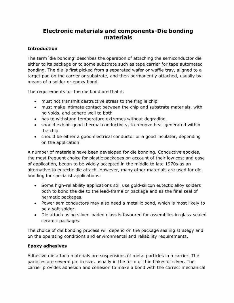
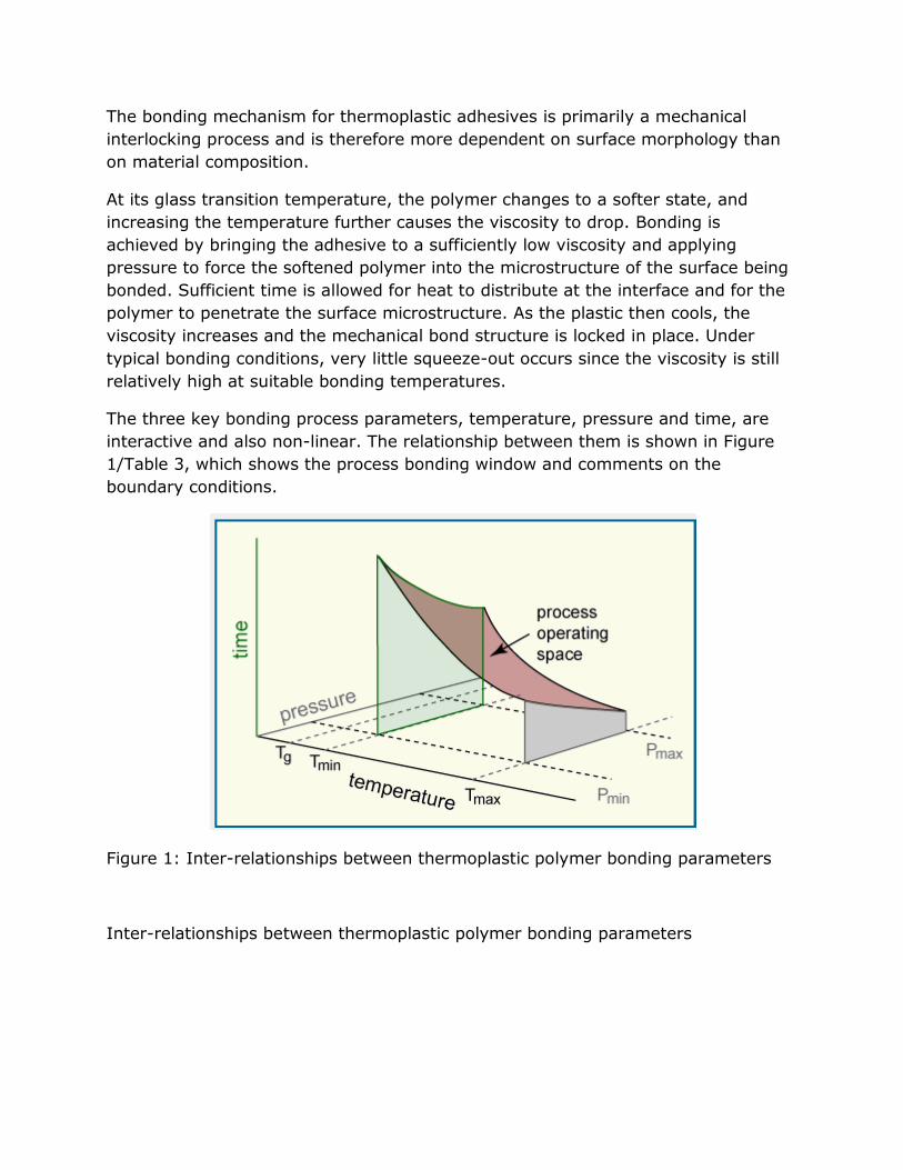
The three key bonding process parameters, temperature, pressure and time, are
interactive and also non-linear. The relationship between them is shown in Figure
1/Table 3, which shows the process bonding window and comments on the
boundary conditions.
Figure 1: Inter-relationships between thermoplastic polymer bonding parameters
Inter-relationships between thermoplastic polymer bonding parameters
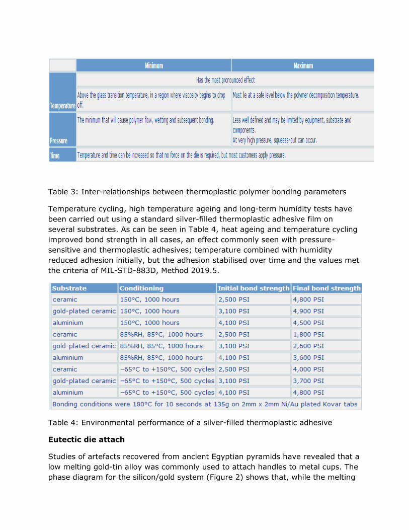
Table 3: Inter-relationships between thermoplastic polymer bonding parameters
Temperature cycling, high temperature ageing and long-term humidity tests have
been carried out using a standard silver-filled thermoplastic adhesive film on
several substrates. As can be seen in Table 4, heat ageing and temperature cycling
improved bond strength in all cases, an effect commonly seen with pressure-
sensitive and thermoplastic adhesives; temperature combined with humidity
reduced adhesion initially, but the adhesion stabilised over time and the values met
the criteria of MIL-STD-883D, Method 2019.5.
Table 4: Environmental performance of a silver-filled thermoplastic adhesive
Eutectic die attach
Studies of artefacts recovered from ancient Egyptian pyramids have revealed that a
low melting gold-tin alloy was commonly used to attach handles to metal cups. The
phase diagram for the silicon/gold system (Figure 2) shows that, while the melting

points of silicon and gold are 1414°C and 1064°C respectively, a eutectic alloy
containing 97.15% gold and 2.85% silicon by weight melts at the comparatively low
temperature of 363°C. [Note that this alloy contains 18.6 atomic per cent of silicon,
because gold is a very much heavier atom]
Figure 2: Phase diagram for the gold-silicon system
In the eutectic die attach process, which was developed during the 1960s, a solder
bond is formed by diffusion between the gold on the package surface and the silicon
of the chip, which are heated and held in intimate contact with each other. The
surfaces of both package and die must be flat enough to allow gold diffusion to take
place.
Typical temperatures are 200°C at the die collet and 400°+C at the heater block
which transmits heat to the package, giving a die attach temperature in the region
375°C–410°C. Higher temperatures are generally recommended as producing
better joints, and sufficient time has to be allowed for the package to reach bonding
temperature.
As the bond-line temperature increases, gold atoms start to diffuse rapidly into the
silicon, and a very thin liquid film forms at the interface once enough gold has
diffused to equal the eutectic composition. As the temperature rises above the
eutectic temperature, a larger volume of eutectic alloy is produced. Alloy formation
continues until one of the two reacting materials is used up, the limiting factor
usually being the gold available from the package.
The die and package are invariably ‘scrubbed’ together: manual bonder operators
became very adept at picking up the die by the side using a pair of fine tweezers,
positioning it in the package cavity and moving it in a semi-circular scrubbing
motion whilst applying light pressure. A visual indication that die attachment is
complete is the presence of eutectic braze around the die perimeter.
Operators have now been almost entirely replaced by machines. Their visual
feedback is substituted for by process controls on time and temperature, and the
scrubbing action is frequently performed by transmitting longitudinal vibration to
the collet. However, a rotary backwards and forwards action gives better wetting
and results in improved yield.
Preforms for eutectic die attach
The gold finish on the substrate is generally the limiting factor:
If the gold is too thin, the bond established will not be very strong.
If the quality of the gold plating is poor, the whole gold surface may be
depleted, breaking the gold-silicon interface. This is a particular hazard
where the gold is incorporated with glass in a thick film conductor.
For this reason it has been industry standard practice to start the reaction and
make more solder available by placing on the substrate a small preform of near
eutectic composition and around 40µm thick. Preform and substrate are heated
above the eutectic temperature, usually to 400°C–425°C: when the preform
becomes a silvery colour, the die is laid on top of the melt and gently agitated.
The procedure is relatively simple and tolerates a range of conditions. However, the
preform needs to wet both the back of the die and the gold on the die bond pad
and this bond is often not continuous, with voids remaining between die and
substrate (Figure 3).

Figure 3: Acoustic microscope images of Au-Si eutectic die attach
Acoustic microscope images of Au-Si eutectic die attach
This shows (left) 45% (right) 20% good die attach by area
Dark areas are well bonded; light areas are unbonded
Investigations have shown that bond failure is accompanied by evidence of poor
wetting between the braze alloy and the gold or silicon surfaces. This can result in
the related (but subtly different) effects of poor mechanical adhesion and high
electrical resistance.
Hoge found the primary cause of poor wetting to be oxidation at interfaces.
Analysis of Auger spectra of typical assembled devices identified silica at the
surfaces of dice and gold-silicon preforms, and oxides of nickel and iron on gold-
metallised substrates. Examination of die and substrates mechanically separated
after die bonding showed that the oxides impair wetting, inhibit silicon diffusion,
and prevent the formation of chemical bonds at the interfaces.
Two inherent difficulties with the gold-silicon preform die attach method are that:
The silicon at the preform surfaces oxidises during heat up and liquid
formation. [This is inevitable unless the ambient is strongly reducing]
The liquid preform may not transmit to the die reverse sufficient shear stress
to remove oxide scales
Evident for the first is that preforms change shape very little during melting and
later solidification, rather than taking the smooth lenticular shape you would expect
from a non-reacting, wetting liquid. This is due to silica (and concentrated traces of
calcium) at the surface forming a ‘skin’ which acts as a barrier to proper wetting
and flow.

Alternative preform materials
Kitchen observed that melting a eutectic preform in contact with gold makes it
gold-rich, causing the overall composition to shift to the left of the eutectic. This
sharply increases the melting point, and has the detrimental effect that the
resulting alloy is in equilibrium with gold rather than silicon. This suggests
substituting alloys containing more silicon that the eutectic. When these are cooled,
crystals of silicon precipitate out, growing until the eutectic temperature is reached,
at which point the remaining liquid forms the eutectic structure. Such alloys would
be in equilibrium with silicon and thus wet the surface of the die. However, adding
only a small amount of silicon to the eutectic significantly increases the melting
point.
Kitchen proposed adding tin to the gold-silicon eutectic. Tin and gold themselves
form a complex system but, if the tin content is limited to 37.4% by weight, the
gold-silicon-tin ternary alloy has the characteristics of a eutectic system. The final
alloy selected was, by weight, 0.35% silicon, 20% tin and 79.65% gold. This has a
melting point of 274°C, and consistently wetted gold-plated surfaces.
Hoge’s alternative approach used an all-gold preform. Compared with gold-silicon:
Only the back of the die will oxidise
Shear stress can be transmitted very effectively from the metallic preform to
the die reverse to remove oxide ‘skin’
The same type of bond can be achieved without a preform by using a lead-frame
selectively plated with thick gold. For lead-frames this form of bonding has several
advantages:
Preforms are often difficult to position and maintain on die bond pads on
lead-frame strips
The preform to substrate interface is eliminated
Less gold is needed to achieve the bond
Eutectic die bonding challenges
There are a number of ways in which the ability of the eutectic solder to wet the
surfaces of package and die may be impaired:
By alloying elements in the surfaces of die and substrate
By oxides on the surfaces of die and substrate. In particular, dice with an
unprotected reverse surface will always have some coating of oxide, the ‘native
oxide’ thickness on exposed silicon being of the order of 2.5nm

By the presence on the surfaces of carbon and organic materials resulting from
exposure to solvents, or poor storage or handling
By contaminants from plating solutions
If the surface of the die is too rough or uneven, and only a few points are in contact
with the gold
If the reacting members oxidise during bonding, undesirable visual defects may be
generated, a problem which can be prevented by carrying out the process in an
inert atmosphere such as nitrogen. Eutectic die bonders usually have a nitrogen or
forming gas blanket at least around the heated stage.
Reverse plating
One way of minimising the effect of both oxide and contamination is to deposit a
layer of gold on the reverse of the wafer, but care must be taken in preparing the
surface and selecting the process, since poor adhesion and non-ohmic contact can
cause rejects. The problem is made worse when:
The gold coating has been evaporated: the alternative ofsputter deposition starts
with a short sputter etch to remove surface impurities
The coating temperature is too high – silicon can diffuse rapidly through grain
boundaries at temperatures as low as 100°C, forming a surface layer enriched in
silicon within only a few minutes. This will subsequently oxidise to form silica.
After deposition, the gold-silicon interface is sometimes alloyed by heating it above
the eutectic temperature, but this can also lead to oxidation of silicon on the
surface, depending on the rate of cooling and level of oxygen in the ambient.
Substrate plating
The gold layer covering die bonding pads is usually plated over a barrier of nickel or
on an alloy containing nickel, such as kovar. Although the rate at which nickel
diffuses through the gold is low at most operating temperatures, the rate of
diffusion at grain boundaries can be quite high, and for this reason nickel oxide is
very often encountered at the surface of gold metallised die bonding pads. Along
with impurities such as organic films, this oxide can impair the wetting of gold-
silicon preforms. In extreme cases, the preforms will not wet at all and will just put
‘ball up’.

Wetting characteristics can be improved with greater surface roughness, although
this may also be associated with non-uniform gold films produced during plating,
which can themselves impair wetting by the preform.
Larger die
Eutectic bonds between large dice and the package can crack as a result of
excessive stress from the TCE mismatch, but the extent of the problem depends
very much on the process and parameters used. Hund and Burchett found that:
Stress is significantly reduced if assemblies are cooled slowly rather than quickly
Shear stresses are much higher for eutectic brazes less than 50µm thick
Cracked die were only observed (under the experimental conditions) for eutectic
braze thicknesses less than 20µm
Tensile and shear stresses in die can be greatly reduced by a stress-relieving
temperature soak at 150°C, followed by slow cooling to room temperature
Soft soldering
A range of commonly used solders is given in Table 5. For power devices, high-lead
materials with elevated melting points are generally preferred, but account has to
be taken of any soldering operations which are to be carried out at the same time,
for example, the assembly of other components in a hybrid microcircuit.
Table 5: Some common soft-soldering materials for die attach
As with surface mount assembly, die attach with soft solders presents the problems
of first getting the solder to the joint and then protecting from oxidation during the
soldering process. Some of the options for this are shown in Table 6.

Table 6: Options for soft-soldering processes for die attach
Although high power devices with as much as 50% voiding may well function within
their electrical specification, reliability is impaired because of stress in the die.
These stresses are quite high, as shown in Figure 4. A typical specification, based
on X-ray inspection, is an allowable maximum of 10% voids, with no individual void
contributing more than 50% of the total.
Figure 4: Maximum principal tensile stresses calculated by FEA techniques
for voids in eutectic attach under the die
Maximum principal tensile stresses calculated by FEA techniques
Moore 1993
Void free soldering depends on the wettability of the surfaces, the accuracy of the
solder volume, and on protecting the process from oxygen, and void levels of 3–5%
can be achieved with appropriate materials and process.
As an alternative to a nitrogen atmosphere, forming gas (nitrogen with 6–10% of
hydrogen) is sometimes used in ovens, although examination of the thermodynamic
properties of the system suggests that hydrogen will not reduce oxides at
temperatures below 400°C.
A high degree of cleanliness in the die bonding operation is required in order to wire
bond and encapsulate successfully:
Flux residues which do not reduce surface resistivity or cause corrosion, may
have an adverse impact on the adhesion of the moulding materials, or even
inhibit the encapsulant curing process leaving soft spots: both tin salts and
amines affect the cure of many encapsulants, particularly silicone
formulations.
Although most users monitor initial bond strength, which will expose
immediate problems of contamination, materials from die mount may
shorten bond wire life.
An intermediate solder
When power devices are operated, the assembly is thermally cycled by changes in
the power input as well as variations in the ambient temperature. This produces
severe stresses where there are large differences in TCE for the materials. A gold-
based ‘hard solder’ joint is relatively strong, so that thermal stresses result in die
fracture, whereas joints made with relatively weaker indium, lead and tin-
containing ‘soft solders’ commonly fail because of thermal fatigue within the joint.
Work by Olsen emphasised the comparative ability of hard solder devices to resist
thermal fatigue as against the steady decline in performance of soft solder devices
shown in Figure 5.
Figure 5: Percentage change in electrical characteristics during power cycling
for hard and soft solders

Percentage change in electrical characteristics during power cycling
However a number of intermediate alloys have been developed, with the aim of
producing a material with a mechanical strength lying between that of hard and soft
solders, avoiding damage to the die whilst resisting thermal fatigue within the joint.
Olsen’s results for ‘Alloy I’ are given in Figure 6.
Figure 6: Percentage change in electrical characteristics during power cycling
for Alloy ‘I’

Percentage change in electrical characteristics during power cycling
‘J Alloy’, with a composition of 25%Ag/10%Sb/65%Sn, aimed at meeting this
requirement, but the additives have limited solid solubility in tin, and both the
normally cooled alloy and foil made from it contain coarse particles of Ag 3 Sn,
some of which are larger than 10µm. During reflow, the tin matrix melts first, and
then dissolves the Ag 3 Sn particles, which have a melting temperature of 480°C.
The longer time and higher temperature needed to dissolve the particles results in
incomplete melting of conventional J alloy during transient heating and cooling.
Tan found that improvements could be made to the material by using a very high
cooling rate. His ‘Rapid Solidification’ process used cooling rates of around 10°C/s,
producing a fine and homogenous microstructure. The same Ag 3 Sn phase was
present, but with the particles finely dispersed. The RS alloy had a well defined
reflow solidification temperature and allows lower soldering temperatures to be
used. Joints prepared with RS alloy foil showed that the finely dispersed
microstructure is retained when appropriate soldering procedures are used.
Solder preforms
Using a soft solder preform, the die can be attached as with gold-silicon eutectic,
and with the same problems. With components, the requirements for a void-free
attach process are normally met by using solder preforms and an atmosphere
which is either inert or reducing. This requires either jigging or clamping of the
assembly.

In vacuum soldering, components are assembled within a graphite block, which is
heated under vacuum by passing a high current through it. Inside the jig are placed
successively the package, a graphite slip with cavities for preform and die, a solder
preform, and the die. The soldering cycle takes typically 10–15 minutes.
For the increasing number of applications which generate substantial heat, the
solder bond must be as free of voids as possible to give minimum thermal
resistance. However, it is almost impossible to achieve void-free bonds when using
solder preforms, since the area of contact between flat and rigid surfaces is rarely
more than 20% of the nominal contact area, and films of air (as thin as 0.1µm) are
invariably trapped at the interfaces. The solder does not flow sufficiently to displace
all this air to the die periphery, and much remains trapped after soldering as voids
within the bond. The larger the bond area, the greater is the potential for air
entrapment.
It was demonstrated with a similar problem in resin-bonded aircraft structures that,
if curing was started in vacuum and the vacuum released when the resin became
fluid, that the voids would collapse, so that the resulting bond was essentially void-
free. Bascom demonstrated that the same ‘vacuum release’ technique could be
used to reduce voids in large area, solder-preform bonding from 50% to less than
10%.
This is because the trapped films are more or less continuous, so that their internal
pressure is reduced when the chamber is first evacuated. When the solder melts
however, surface tension and gravitational forces cause the solder to flow into this
space and segregate the air into discrete bubbles. If the chamber is returned to
atmospheric pressure whilst the solder is still molten, hydrostatic pressure will
collapse the voids and considerably reduce their volume.
If the molten solder has wetted well to the substrate, and the solder viscosity is
sufficiently low, the trapped air pockets and resulting voids will be displaced from
the interface. The aircraft experiment suggests that, even with poor wetting, void
elimination would still occur, the hydrostatic forces overwhelming the surface
forces, but that the collapsed voids would be trapped at the interface.
Providing solder as a preform involves handling, and it is possible instead to deposit
suitable materials on the die reverse. Work has been carried out using lead-tin
materials, with a gold outer layer to protect from oxidation, and a chromium seed
layer to enhance bonding to the reverse of the wafer. Coating is carried out at high
vacuum to prevent oxidation of the tin.
Solder paste for die attach
A major drawback is that solder pastes contain around 50% by volume of flux
vehicle: either this must leave no residue after soldering, or the residue must be
totally removable. Given that water-based pastes contain more aggressive fluxes
than rosin-based systems, and that solvent cleaning tends to leave residues, the
choice is generally between zero residue and water-soluble products.
The volume and shape of the paste deposit is important:
In contrast to surface mount solder terminations, which have a small area
but large vertical fillets, die attach solder needs to be thinly spread over a
large area
Stencil printing is therefore the preferred process.
For small components, the stencil aperture should be less than the die size
For larger die, a modified St Andrew’s cross shape is favoured as this both
supports the squeegee and generates minimum voids, in the same way that
a similar pattern is commonly used when dispensing resin.
The die attach system needs control of the force applied to the die in order to
produce a defined bond line thickness, and a practical automatic bonder for
hermetic packages may need a depth sensor to allow for variations in cavity depth.
Solder reflow issues
There are three critical phases in solder paste reflow for die attach:
The temperature rise on entry must be slow enough to prevent fast
outgassing and maintain correct die orientation
The temperature ‘spike’ must be sufficient to heat the solder paste quickly
and take it to reflow without drying out the flux
In the cooling zone, the rate of temperature fall should be as slow as
possible, in order to reduce thermal stress
Fenner has reported that, in order to allow the solder to wet the entire reverse of
the die, the assembly needs to be above liquidus for longer than with conventional
surface mount. This is demanding on the flux activation system, and a rapid ramp
is required to keep process time low and avoid flux exhaustion before the soldering
is complete. The process parameters are however just within the acceptable range
for regular surface mount, so bare dice can be processed alongside conventional
components in a single reflow operation.

An alternative view is that the solder alloy being liquid for some time produces a
crystalline structure with relatively large particles, with the result that cracks easily
develop along the boundaries during thermal cycling. If a short liquid phase of
perhaps 12–13 seconds can be used, the alloy will remain fine-grained and
homogenous, giving better thermal cycling performance. Unfortunately, this is not
compatible with simultaneously performing surface mount assembly.
Silver-glass
Silver-glass adhesives are a potential substitute for gold-silicon eutectic, as they
have high thermal conductivity and a TCE close to that of silicon. Silver-glass has
been evaluated for the manufacture of power hybrids, and for attaching active
devices with gold or silver back metallisation to substrates which are metallised
with nickel or silver-plated copper.
A typical silver-glass paste contains 80–85% by weight of silver flake and lead
borate glass dispersed in a organic vehicle system. The paste is dispensed into the
package cavity, the die placed on the paste, and the package inserted in a furnace.
The heat removes the organic vehicle, and then centres the residual solder and
glass to bond the die strongly to the ceramic.
The bond material must form a smooth fillet, and the bond must be free of voids
and cracks: to achieve this, the conventional process includes a pre-drying step of
from 2–10 hours at 60–80°C, depending on die size. Sufficient solvent needs to be
eliminated to avoid the formation of voids, and the void density depends on the
drying temperature. However, too high a drying temperature can result in reduced
shear strength because there is no intimate contact between die and glass. With
optimised conditions, an X-ray non destructive test by Dequidt revealed voids less
than 1%.

Figure 7 illustrates the sequence of events which happen to silver glass paste
during firing. Solvent evaporation (50–200°C) is followed by polymer resin burn-out
(300°C). The glass starts to soften at 340°C, which causes silver-glass sintering to
accelerate and further wet the surfaces of die and substrate. Reaction bonding of
silver-glass with silicon and alumina also starts at about 340°C, and the reaction is
completed when the temperature has been maintained at 410–430°C for
approximately 10 minutes.
Figure 7: Firing profile for silver-glass
Firing profile for silver-glass
Shear strength increases with sintering temperature towards an asymptotic value,
probably due to the densification of silver particles. A compromise is therefore
necessary between the optimum temperature and the maximum acceptable for the
silicon die before the aluminium to silicon ohmic contact starts to degrade.
SEM observation shows that the attachment to the die is not continuous, that there
is a high concentration of lead at the interface between the silver-glass and the
substrate, and adhesion seems to be the result of diffusion of silver into the gold
layer. Dequidt explained the absence both of gold in the silicon and of any gold-
silicon eutectic by the nickel or titanium under-layer preventing migration of gold
into the silicon. Similarly, bonds between the silver glass and the plated package
are probably interdiffusion mechanisms, whereas bonds between alumina and silver
glass are chemical and similar to conventional thick film.

In investigating the process, thermogravimetric analysis (TGA) is used to determine
the temperature at which solvents are eliminated from the binder, and differential
thermal analysis (DFA) to characterise the glass and show its recrystallisation.
Developments in silver-glass die attach materials have aimed to produce:
stress relief for large area dice
a single pass firing process with no pre-drying
precise rheology for high speed dispensing
lower firing temperature
As with resin attach, provided that the thickness and modulus of the die bonding
material is small compared to the thickness and moduli of die and substrate, the
TCE of the bonding material is not a significant factor in die stress. However, cracks
due to thermally induced stresses arising from a TCE mismatch between silicon and
ceramic have been reported by Nguyen for die larger than 10mm side, and the
bond line thickness has to exceed a minimum value for acceptable performance.
The stress in the bonding material is related to the sintering behaviour of the
silver/lead borate glass mixture. Control of the sintering rate is typically achieved
by small quantities (0.1–1%) of proprietary additives which increase the surface
roughness and slow down regrouping of the particles. This helps to eliminate cracks
without adversely impacting on adhesion and void formation.
Despite the claim that silver-filled glass offers lower cost, faster processing, high
yield, better thermal performance, and a lower die stress than gold-silicon eutectic,
it has not replaced eutectic or other solders for high power chips. This seems to be
because companies are reluctant to change. The material is however widely used in
the fabrication of CerDIP packages, on account of its resistance to the high
temperature of the furnace sealing involved.
Author: Martin Tarr
Source: http://www.ami.ac.uk/courses/topics/0203_dbm/index.html