Electronic Circuits for Switching-Time Reduction of ...€¦ · Electronic Circuits for...
15
Electronic Circuits for Switching-Time Reduction of Bipolar Semiconductor Devices N. Y. A SHAMMAS, S.EIO, D. CHAMUMD Staffordshire University, Stafford, UK, [email protected] , www.staffs.ac.uk Abstract: Bipolar semiconductor devices are often used as switches in very high power electronic circuits and systems. They have replaced the old conventional gas filled tubes and vacuum devices in many applications. This is mainly due to the fact that solid-state devices are more efficient, smaller in size, cheaper and more reliable. In addition, solid-state devices are considered environmental friendly, since they do not contain nasty gases and toxic materials used in old devices. The power level requirements and switching frequency are continually increasing in the power electronic industry, and this demands larger and faster switching devices. As a result, both bipolar and unipolar semiconductor devices have undergone continued improvement in current and voltage ratings, and switching speed. The main advantage of bipolar devices is their low conduction losses due to conductivity modulation, but their main disadvantage is the high switching losses which is due to minority carrier injection. The Insulated Gate Bipolar Transistor (IGBT) combines the advantages of both unipolar and bipolar devices. It has a simple gate drive circuit like that of the MOSFET, with high current and low saturation voltage capability of bipolar transistor. The main problem remains with the relatively long tail turn-off current. To reduce the turn-off time of the IGBT and other bipolar devices, different lifetime control techniques and structural changes have been developed and used. Details of these and new techniques developed by using auxiliary electronic circuits for reducing the turn-off time and increasing the switching speed of bipolar semiconductor devices are presented in this paper. Key-Words: - power semiconductor diodes, thyristors, Insulated gate bipolar transistors, Proceedings of the 13th WSEAS International Conference on CIRCUITS ISSN: 1790-5117 28 ISBN: 978-960-474-096-3
Transcript of Electronic Circuits for Switching-Time Reduction of ...€¦ · Electronic Circuits for...

Electronic Circuits for Switching-Time Reduction of Bipolar Semiconductor Devices
N. Y. A SHAMMAS, S.EIO, D. CHAMUMD
Staffordshire University, Stafford, UK, [email protected], www.staffs.ac.uk
Abstract: Bipolar semiconductor devices are often used as switches in very high power electronic circuits and systems. They have replaced the old conventional gas filled tubes and vacuum devices in many applications. This is mainly due to the fact that solid-state devices are more efficient, smaller in size, cheaper and more reliable. In addition, solid-state devices are considered environmental friendly, since they do not contain nasty gases and toxic materials used in old devices. The power level requirements and switching frequency are continually increasing in the power electronic industry, and this demands larger and faster switching devices. As a result, both bipolar and unipolar semiconductor devices have undergone continued improvement in current and voltage ratings, and switching speed. The main advantage of bipolar devices is their low conduction losses due to conductivity modulation, but their main disadvantage is the high switching losses which is due to minority carrier injection. The Insulated Gate Bipolar Transistor (IGBT) combines the advantages of both unipolar and bipolar devices. It has a simple gate drive circuit like that of the MOSFET, with high current and low saturation voltage capability of bipolar transistor. The main problem remains with the relatively long tail turn-off current. To reduce the turn-off time of the IGBT and other bipolar devices, different lifetime control techniques and structural changes have been developed and used. Details of these and new techniques developed by using auxiliary electronic circuits for reducing the turn-off time and increasing the switching speed of bipolar semiconductor devices are presented in this paper.
Key-Words: - power semiconductor diodes, thyristors, Insulated gate bipolar transistors,
Proceedings of the 13th WSEAS International Conference on CIRCUITS
ISSN: 1790-5117 28 ISBN: 978-960-474-096-3
1 Introduction Power electronic system generally involves a source of energy, which is released to the load by means of a switching device (Figure1). The limiting device in high power electronic system is often the switch, which limits the peak current, voltage and the repetition rate. The switching element is very special and falls into two basic categories: � Vacuum and Gas filled switching tubes, � Solid-state (semiconductor) switches The conventional approach in very high power designs is to use a gas filled switch such as a thyratron, ignitron or spark gap. However these devices have limited lifetime, high cost, low repetition rate and high losses. On the other hand high power semiconductor devices have under gone continued improvement in switching speed, voltage and current rating and thus are replacing the conventional gas filled devices in many applications. For very high power applications such as high voltage direct current (HVDC) systems, series and parallel connection of these devices are used for high voltage and current respectively. Full details of methods used and problems encountered for IGBT connections as an example are given in reference (1). The power level requirements and switching frequency are continually increasing in the power electronic industry, and this demands larger and faster switching devices. As a result, both bipolar and unipolar semiconductor devices have undergone continued improvement in current and voltage ratings, and switching speed. The main advantage of bipolar devices is their low conduction losses due to conductivity modulation. But their main disadvantage is the high switching losses and the slow speed of
recovery, which is due to minority carrier injection during the conduction state. The Insulated Gate Bipolar Transistor (IGBT) combines the advantages of both. It has a simple gate drive circuit like that of the MOSFET, with high current and low saturation voltage capability of bipolar transistor. The main problem remains with the relatively long tail turn-off current. To reduce the turn-off time of the IGBT and other bipolar devices, different lifetime control techniques and structural changes have been developed and used. A general brief description of the above mentioned devices, and details of new techniques developed by using auxiliary electronic circuits with semiconductor devices for reducing the turn-off time and increasing the switching speed of bipolar devices are given in the following sections. 2 Vacuum and gas-filled devices Two primary distinguishing features can classify these types of switches: � the source of free electrons within the device and � the gaseous filling (or lack of it) within the tube envelope. A vacuum tube is a device with a vacuum (very low pressure gas) filling. And a gas filled device is filled with gas that might be at a pressure somewhat above or below atmospheric. The type of gas used is also an important feature, particularly in switching tubes where a wide variety of fillings are encountered. The source of the free conduction electrons in the device may be either thermal such as a heated filament – a hot cathode, or alternatively a simple consequence of a high voltage gradient across the device, resulting in auto-emission from the
Proceedings of the 13th WSEAS International Conference on CIRCUITS
ISSN: 1790-5117 29 ISBN: 978-960-474-096-3

cathode. A device employing this latter method is known as a cold cathode device and is used in many high-voltage switching circuits. 2.1 Thyratrons It is a type of gas filled tube used as a high energy switch. Triode, Tetrode and Pentode variations of the thyratron have been manufactured in the past though most are of the triode design. Gases used include mercury vapor, xenon, neon, and (in special high-voltage applications or applications requiring very short switching times) hydrogen. Unlike a vacuum tube, a thyratron cannot be used to amplify signals linearly. Thyratrons evolved in the 1920s from early vacuum tubes A typical hot-cathode thyratron uses a heated filament cathode, contained within a shield assembly with a control grid on one open side, which faces the plate-shaped anode. When positive voltage is applied to the anode, and the control electrode is kept at cathode potential, no current flows. When the control electrode is made positive with respect to the cathode, the gas between the anode and cathode ionizes and conducts current. The shield prevents ionized current paths that might form within other parts of the tube. The gas in a thyratron is typically at a fraction of the atmospheric pressure ; 15 to 30 milli bars is typical. Both hot and cold cathode versions are encountered. A hot cathode is an advantage, as ionization of the gas is made easier; thus, the tube’s control electrode is more sensitive. Once turned on, the thyratron will remain on (conducting) as long as there is a significant current flowing through it. When the anode voltage or current falls to zero, the device switches off. Large thyratrons are still manufactured, and are capable of operation up to tens of
kiloamperes (kA) and tens of kilovolts (kV). Modern applications include pulse drivers for pulsed radar equipment, high-energy gas lasers, radiotherapy devices, and in Tesla coils. Thyratrons are also used in high-power UHF television transmitters, to protect inductive output tubes from internal shorts, by grounding the incoming high-voltage supply during the time it takes for a circuit breaker to open and reactive components to drain their stored charges. This is commonly called a “crowbar” circuit. Thyratrons have been replaced in most low and medium-power applications by corresponding semiconductor devices (Thyristors ). 2.2 Ingnitron It is a type of controlled rectifier dating from the 1930s. It is usually a large steel container with a pool of mercury acting as a cathode. A large graphite cylinder, held above the pool by an insulated electrical connection, serves as the anode. An igniting electrode (ignitor) is briefly pulsed to create an electrically conductive mercury plasma, triggering heavy conduction between the cathode and anode. Ignitrons were long used as high-current rectifiers in major industrial installations where thousands of amperes of AC current must be converted to DC, such as aluminium smelters. Because they are far more resistant to damage due to over current or back-voltage, ignitrons are still manufactured and used in preference to semiconductors in certain installations. They are often used to switch high energy capacitor banks for emergency short-circuiting of high voltage power sources (crowbar).
Proceedings of the 13th WSEAS International Conference on CIRCUITS
ISSN: 1790-5117 30 ISBN: 978-960-474-096-3
2.3 Krytron It is a cold-cathode gas filled tube intended for use as a very high-speed switch. The krytron uses arc discharge to handle very high voltages and currents (several kV and several kA), rather than the usual low-current glow discharge. There are four electrodes in a krytron. Two are conventional anode and cathode. One is a keep-alive electrode, arranged to be close to the cathode. The keep-alive has a low positive voltage applied, which causes a small area of gas to ionize near the cathode. High voltage is applied to the anode, but primary conduction does not occur until a positive pulse is applied to the trigger electrode. Once started, arc conduction carries a considerable current. In place of or in addition to the keep-alive electrode some krytrons may contain a very small amount of radioactive material (usually nickel-63) which emits beta particles (high-speed electrons) to make ionisation easier. This design, dating from the late 1940s, is still capable of pulse-power performance which even the most advanced semiconductors (even IGBT transistors) cannot match easily. The vacuum-filled version is called a Sprytron and is designed for use in environments where high levels of ionising radiation are present (because the radiation might cause the gas-filled krytron to trigger inadvertently). 2.4 Over voltage spark-gap It is essentially just two electrodes with a gap in between. When the voltage between the two electrodes exceeds the breakdown voltage, the device arcs over and a current is very rapidly established. The voltage at which arcing occurs is given by the Dynamic Breakdown Voltage for a fast rising impulse voltage. Note that this voltage may be as much as 1.5 times greater than the static breakdown voltage (breakdown voltage for a slowly rising
voltage.), a shorter rise time means a higher breakdown voltage. Commutation times for these devices are exceptionally low (sometimes less than 1 nanosecond). Overvoltage gaps are primarily used for protection. But in combination with the other devices mentioned here they are commonly used to sharpen the output pulses (decrease the rise times) of very high current pulses form triggered switching devices e.g. Thyratrons. The size of these devices is almost entirely dependent upon how much current/voltage they are intended to switch, There is no limit as to the size of these devices. 2.5 Triggered spark-gap It is a simple device; a high voltage trigger pulse applied to a trigger electrode initiates an arc discharge between anode and cathode. This trigger pulse may be utilized in a variety of ways to initiate the main discharge. Different triggered spark gaps are so designed to employ one particular method to create the main anode to cathode discharge. The different methods are as follows: i) Electric field distortion: three electrodes; employs the point discharge (actually sharp edge) effect in the creation of a conducting path. ii) Irradiated: three electrodes; spark source creates an illuminating plasma that excites electrons between the anode and cathode. iii) Swinging cascade: three electrodes; trigger electrode nearer to one of the main electrodes than the other. iv) Mid plane: three electrodes; the trigger electrode is centrally positioned. v) Trigatron: trigger to one electrode current forms plasma that spreads to encompass a path between anode and cathode. The triggered Spark gap may be filled with a wide variety of materials, the
Proceedings of the 13th WSEAS International Conference on CIRCUITS
ISSN: 1790-5117 31 ISBN: 978-960-474-096-3
most common are: Air, Argon, and SF6. Often a mixture of the above materials is employed. However a few spark gaps actually employ liquid dielectric (e.g. they might be immersed in oil)or even solid media fillings. Solid filled devices are often designed for single shot use. Usually Gas filled spark gaps operate in the 20-100kV / 20 to 100kA range. Spark gaps are damaged by repeated heavy discharge. This is an inevitable consequence of such high discharge currents. Electrode pitting being the most common form of damage. Between 1 and few thousand shots per device is usually about what is permissible before damage begins to severely degrade performance.. Laser switching of spark gaps: The fastest way to switch a triggered spark gap is with an intense pulse of Laser light, which creates plasma between the electrodes with extreme rapidity. 3 Power Semiconductor Switches These generally fall into three categories viz. bipolar devices (such as pn junction diodes, BJT transistors, thyristors), unipolar devices (such as Schottky diodes and Power MOSFETS) and Bi-MOS devices such as IGBTs (which is a combination of MOSFET and Bipolar Devices).
3.1 Power Diodes Power diodes are basically two terminals (anode and cathode) uncontrolled switches and they are turned ON and OFF by the action of the electrical circuits. A fundamental property of a diode is its rectifying characteristics as shown in figure 2. This means it has two modes of operation, i.e. forward conduction mode (ON-State) and reverse blocking mode (OFF-State). In the ON-State it conducts a current ION and has a finite on-state voltage drop VON. This
results in significant power dissipation in the diode and consequently limits the maximum current handling capability. In the reverse blocking mode it exhibits a finite blocking current and also supports a finite maximum reverse voltage (reverse breakdown voltage BVR). Power loss due to blocking current is small but can become significant at high operating temperature. A diode also has finite switching times during turn-on and turn-off leading further power losses in the device. There are basically two types of power diodes, a p-n junction diode and a Schottky barrier diode. A p-n junction diode is a two-layer semiconductor device usually formed by diffusing p-type impurities into n-type silicon. The interface between p-type and n-type silicon is called p-n junction and hence the p-n junction diode. With this type of structure very high current and very high voltage diodes can be manufactured (> 10,000A and >9kV). Power diodes are supplied in variety of packages e.g. metals, plastics and ceramic housings. For high power applications, devices in ceramic housing are often used. The Schottky barrier diode is formed by producing a metal-semiconductor junction as a Schottky barrier (unlike p-n junction in semiconductor to semiconductor junction). This structure results in very fast switching device with low forward voltage drop. However Schottky diodes based on silicon material gives low reverse blocking characteristics (~50V) and hence not quite suitable for very high voltage application. However recent development is replacing silicon in favour of other semiconductor material such as silicon carbide and diamond to increase the reverse blocking characteristics of these diodes.
Proceedings of the 13th WSEAS International Conference on CIRCUITS
ISSN: 1790-5117 32 ISBN: 978-960-474-096-3

The main application of power diode is rectification of AC to DC power, and commutation of inductive power in many power conversion circuits.
3.2 Power Thyristors The thyristor is a solid-state semiconductor device with four layers of alternating N and P-type material. They act as a switch with three terminals (anode, cathode and gate), conducting when their gate receives a current pulse, and continue to conduct for as long as they are forward biased. Thyristor has three modes of operation (Figure 3), the forward blocking mode, the reverse blocking mode and forward conduction mode when triggered on. That is why it is also known as silicon-controlled-rectifier (SCR). Thyristors are well suited for AC circuit applications because they have forward and reverse blocking characteristics and when triggered on in the forward direction they turn off naturally upon reversal of the anode voltage. The thyristor can be made to operate in DC circuit but some external means to turn off is required such as commutation circuit. For DC circuit applications, it is preferable to be able to turn-off the current flow without reversal of the anode voltage. This has been achieved in a structure called the Gate Turn-Off (GTO) Thyristor. Other useful structures belonging to the thyristor family are the ASCR asymmetrical thyristors, IGCT — Integrated gate commutated thyristor, LASCR — light activated SCR, or LTT — light triggered thyristor.
3.3 IGBT Modules Insulated Gate Bipolar Transistor (IGBT) combines the simple gate drive characteristics of the MOSFET with the high current and low saturation voltage capability of bipolar transistors
by combining an isolated gate FET for the control input, and a bipolar power transistor as a switch, in a single device. The IGBT is mainly used in switching power supplies and motor control applications. Figure 4 shows the output characteristics of IGBT. IGBT has three modes of operation, forward blocking mode, reverse blocking mode and forward conduction mode. Most IGBTs on the market have asymmetrical blocking characteristics i.e. very little or no reverse blocking capability. The IGBT is a recent invention. The “first-generation” devices of the 1980s and early ‘90s were relatively slow in switching, and prone to failure through such modes as latch up and secondary breakdown. Second-generation devices were much improved, and the current third-generation ones are even better, with speed rivaling MOSFETs, and excellent ruggedness and tolerance of over-loads. The extremely high pulse ratings of second- and third-generation devices also make them useful for generating large power pulses in areas like particle and plasma physics, where they are starting to supersede older devices like thyratrons and triggered spark gaps. Figure 5 shows IGBT module which houses several IGBT chips connected in parallel to obtain high current rating. For high voltage applications, series connection of IGBTs is required[1]. 4 Fast switching Solid-State Devices The power electronics industry has an escalating appetite for bipolar semiconductor devices with high breakdown voltages, high current ratings and fast switching speeds. High voltage devices are required to have long carrier lifetime to reduce its on-state losses, however short carrier
Proceedings of the 13th WSEAS International Conference on CIRCUITS
ISSN: 1790-5117 33 ISBN: 978-960-474-096-3
lifetime are also required to increase the switching speed of a given device. Therefore, commonly used devices such as power diodes, thyristors and IGBTs are required to have the combination of high breakdown voltages, high current handling ability and high switching speeds. Power electronic applications can be made more efficient by increasing the switching frequency of the semiconductor device used in the electronic circuits. Some of the frequently used devices such as power diodes, thyristors and IGBTs produce turn-off transients that limit their switching frequency. To reduce the turn-off transient produced, carrier lifetime control technique is one of the frequently used techniques to reduce the reverse recovery time of power diodes and thyristors, and also used to reduce the tail current of IGBTs. This technique is based on increasing the recombination centres in the device and is implemented during its manufacturing stages to reduce its switching transients, however this can lead to unwanted changes to the device parameters. Power diodes and thyristors produce a reverse recovery charge during their turn-off time that limits its switching frequency. The reverse recovery charge is caused by the increase in the device width that is required to accommodate higher breakdown voltages [2, 3]. This increased width stores excess carriers during the forward conduction of the device and prevents the formation of a reverse blocking junction, which also lengthen the turn-off time as a result of conducting large negative current [4]. Therefore, the reduction in the reverse recovery charge can reduce the turn-off time of the device [5]. The turn-off time of the device can be effected by many external circuit factors and internal device parameters
[6, 7]. External circuit parameters are the circuit operation and layout, stray inductances, applied voltage, commutating di/dt, forward current, and junction temperature. All of these external circuit parameters can be optimised during circuit design [7]. Internal device parameters which includes device geometry, doping profile and minority carrier lifetime can only be optimised during the device manufacturing stages [4, 8]. One of the frequently used techniques in reducing the turn-off time of semiconductor device is by controlling the carrier lifetime. This technique introduces recombination centres into the device structure by either doping process or high energy irradiation to reduce the carrier lifetime of the device that results in the reduction in turn-off time [5, 9, 10]. Carrier lifetime control technique is also frequently used to reduce the turn-off time in IGBTs [11]. The turn-off time of IGBTs are largely caused by a current tailing effect that is a result of excess carriers stored in the device’s N-base region during its forward conduction [12, 13]. These stored carriers requires a finite time for the carriers within to recombine to its normal state of equilibrium and therefore, introducing recombination centres into the device can reduce the device turn-off time [14, 15]. Control of carrier lifetime is an effective technique in reducing the turn-off time in bipolar semiconductor devices where its objective is achieved by increasing the recombination centres that reduces the carrier lifetime. However the implementation of carrier lifetime control techniques can result in a trade-off between device parameters where high voltage devices require a long carrier lifetime to reduce on-state losses [16, 17 and 18], and reducing the carrier lifetime can increase the on-state losses. Therefore, the proposed
Proceedings of the 13th WSEAS International Conference on CIRCUITS
ISSN: 1790-5117 34 ISBN: 978-960-474-096-3

current injection technique described in the following section has the effect of increasing the recombination centres of the given device during its turn-off transient only. 5 The Current Injection Technique The principle behind the current injection technique is to inject an opposing current to a given power diode and thyristor, or an IGBT during its turn-off transient. To do this at a precise time, an external circuit that is capable of detecting and injecting the opposing current from a pre-charged capacitor into the DUT, at a predetermined level of the anode or collector current is required. The detecting function of the circuit is realized with a current detection and triggering circuit that controls the trigger time and period of a current injection circuit. 5.1 Current Detection and Triggering Circuit The turn-off time of power diodes, thyristors and IGBTs are usually in the range of microseconds or less, which means only very short electronic delays in the current detection and triggering circuit can be tolerated. Therefore, a fast speed operation amplifier (THS3202) was connected in a voltage comparator circuit to trigger a current injection circuit into conduction while isolated with an opto-coupler type (HCNW3120). The anode or collector current of the DUT was measured with a current transducer and its output signal was compared with a reference level using the mentioned operational amplifier. 5.2 Current Injection Circuit Figure 6 shows the current injection circuit proposed for power diodes and thyristors, while figure 7 shows the current injection circuit proposed for IGBTs. When the current injection
circuit receives a triggering pulse from the detection and triggering circuit, the IGBT (IRGPC50S) that controls the switching operation in the circuit conducts and injects a current of a predetermine amplitude from a pre-charged capacitor (C3) into the DUT, limited by the resistor Ri. 6 Experimental Test and Results Prior to implementing the current injection technique on a given power diode (1N5401), thyristor (50RIA120) and an IGBT (IRGPC50S), a previously published switching transient test circuit was reconstructed to simulate the turn-off transient of a given power diode and the same circuit was modified for the thyristor [7]. A resistive load test circuit that was designed for IGBT parameter extraction was reconstructed to simulate the IGBT turn-off transient [19]. 6.1 Power diode switching transient test circuit The Device under Test (DUT) shown in figure 8 is a 1N5401 power diode; it was subjected to a steady state forward current of 1.1A for a period of 2ms and then followed by the application of 70V DC reverse bias voltage. The forward current was applied by switching the IRGPC50S IGBT into forward conduction with the 15Vdc gate pulse shown in figure 9 (CH II). At the end of the period this pulse, a thyristor (30TPS12) was switched into conduction with its triggering gate pulse shown as CH I of the mentioned figure; this applied a 70V DC reverse bias voltage on the DUT and forcing the DUT into its reverse recovery state. This circuit is capable of demonstrating the effects of the circuit parameters and operating conditions of the reverse recovery [7]. In this circuit, two high voltage and low inductance capacitors (C1, C2) with ratings of 1.2kVdc,
Proceedings of the 13th WSEAS International Conference on CIRCUITS
ISSN: 1790-5117 35 ISBN: 978-960-474-096-3
20nH and 200uF were charged to provide variable high voltage testing up to 1kV. The voltage across the capacitors was measured with 1.2kV digital multi-meters and the anode current of the DUT was obtained with a wideband current transducer (CT), while the voltage across the DUT was obtained with a Tektronix high voltage probe of 120MHz bandwidth and 1.5kV rating. Both the CT and high voltage probe are connected to a Tektronix’s TDS3054B 4 channel digital phosphor oscilloscope. The anode current obtained during the DUT’s turn-off transient was practically simulated with the circuit diagram shown in figure 8 and its anode current waveform shown in figure 10, labelled as ‘Original DI’. 6.2 Power Diode with the Implementation of the Current Injection Technique The current inject circuit shown in figure 6 was implemented into the power diode switching transient test circuit in figure 8, as highlighted in dotted lines. The anode current obtained during the turn-off transient of the DUT with the current injection circuit is shown in figure 10 and labelled as ‘CI Method DI’ waveform. Comparing the two waveforms in figure 10, a reduction in the DUT’s reverse recovery time from 6.5us to 4us and peak reverse recovery current from -1.27A to -0.09A was achieved with the addition of the current injection circuit. This indicates a 96% reduction in the reverse recovery charge from 4.13uC to 0.18uC (as calculated from equation 1 below), 38% reduction in the reverse recovery time and a 93% reduction in the peak reverse recovery current.
2trrIpkrQrr ×
=
(1) Where
Qrr is the reverse recovery charge
Ipkr is the peak reverse recovery current
trr is the reverse recovery time
6.3 Thyristor switching transient test circuit The power diode switching transient test circuit was used to simulate the turn-off transient of the thyristor (50RIA120) used as the Device under Test (DUT) by modifying the circuit shown in figure 11. The anode current obtained during the DUT’s turn-off transient is shown in figure 13 labelled as ‘Original THY’. The triggering gate pulse of the forward bias circuit’s IGBT is (CH I), the gate pulse to trigger the DUT (CH II) and the gate pulse to trigger the reverse bias circuit’s Thyristor (CH III) are shown in figure 12. This circuit bias the DUT to conduct a 1.1A forward current for a period of 2ms and then forces the DUT into its reverse recovery state with the application of a 70Vdc reverse bias voltage. 6.4 Thyristor Implementation of Current Injection Technique The current injection circuit shown in figure 6 was implemented into the thyristor switching transient circuit as shown in figure 11 with the added auxiliary circuit highlighted with dotted lines. The anode current obtained during the turn-off transient of the DUT is shown in figure 13, labelled as ‘CI Method THY’. Comparing the two anode current waveforms, a significant reduction in the reverse recovery time from 29us to 3us and the amplitude of
Proceedings of the 13th WSEAS International Conference on CIRCUITS
ISSN: 1790-5117 36 ISBN: 978-960-474-096-3
the peak reverse recovery current from -1.1A to -0.17A can be seen. This indicates a 98% reduction in the reverse recovery charge from 15.95uC to 0.25uC (equation 1), 89% reduction in the reverse recovery time and a 79% reduction in the amplitude of the peak reverse recovery current. 6.5 Power diode and thyristor results discussion Practical results obtained from these experiments suggest that the turn-off time of power diodes and thyristors can be reduced by the application of an the injected opposing current to the device during its turn-off time. This is because opposing current reduces the reverse recovery charge and the amplitude of the peak reverse recovery current, which both contributes to the reverse recovery time of the DUT. Where the reverse recovery charge and the amplitude of the peak reverse recovery current are dependent on the time that are required for the stored charge in the drift region to recombine to its normal state and allowing the reverse blocking junction to be restored. To shorten this time, carrier lifetime control technique are frequently used to introduce recombination centres in the device. This in turns reduce the peak reverse recovery current, reverse recovery charge and the reverse recovery time. However, it also changes required the device parameters during the steady state of the DUT. The principle behind the current injection technique is also to reduce the turn-off time of the reverse recovery charge and the stored charge by introducing additional recombination centres in the DUT only during its turn-off transient. This can be explained with figure 14, where the carrier distribution in the device is shown. During the turn-off transient, the carrier distribution gradually reduces as shown
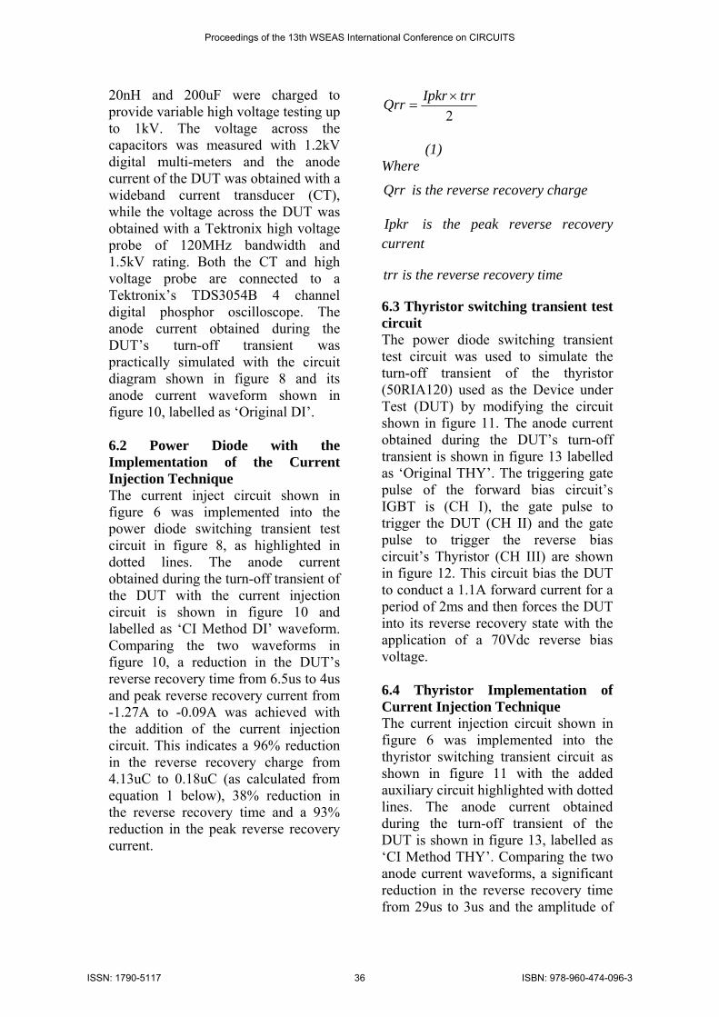
with full lines and results in stored charges in the DUT. These stored charges prevents the DUT from blocking a reverse bias voltage and therefore allowing the DUT to conduct a negative current when both hole and electron currents are being extracted from the DUT when a reverse bias voltage is applied on the DUT. Therefore, the application of an opposing current during the turn-off transient of the DUT injects additional hole and electron current into the device and temporary increasing the recombination centres in the device to cancel the existing electron and hole current. This assists the DUT by preventing it from conducting large negative current. 6.6 IGBT switching transient test circuit A resistive load circuit that was previously developed for extracting the parameters of IGBTs was reconstructed to simulate the turn-off transient of an IGBT (IRGPC50S) denoted as the Device under Test (DUT) in figure 15. The two 15Vdc pulses shown in figure 16 is the gate pulse of the DUT labelled with CH I and the gate pulse of IGBT T1 (CH II). The IGBT (T1) was used to protect the DUT and the voltage source in an event of a device breakdown. When the circuit is closed, the DUT conducts a 1A current for a period of 2ms. The capacitor used (C2) was a high voltage (1.2kVdc), low inductance (20nH) capacitor that was pre-charged to provide the variable applied voltages to the DUT. The collector current of the DUT was measured with the current transducer and the voltage across the device was obtained with a Tektronix high voltage probe that is similar to the one used in previous sections of this paper. The collector current of the DUT obtained during its turn-off transient is shown in figure 17, labelled as ‘Original IGBT’.
Proceedings of the 13th WSEAS International Conference on CIRCUITS
ISSN: 1790-5117 37 ISBN: 978-960-474-096-3

6.7 IGBT Implementation of Current Injection Technique The current injection circuit for IGBT (shown in figure 7) was implemented into the IGBT switching transient test circuit, as highlighted with dotted lines in figure 15. The collector current of the DUT obtained during its turn-off transient is shown in figure 17, labelled ‘CI Method IGBT’. Comparing the ‘Original IGBT’ waveform and the ‘CI Method IGBT’ waveform, an 80% reduction in the time where the amplitude of the collector tail current fall to zero from 1.2us to 0.2us can be seen, indicating a reduction in the DUT’s turn-off time. 6.8 IGBT discussion Experimental results show that the application of an opposing current into the DUT can reduce the time required for the IGBT collector tail current to reach the amplitude of zero. Previous studies showed that IGBT current tailing is caused by store charge in the n-base region of the device and requires a finite time to recombine to its normal state, as discussed previously. Therefore, implementing the carrier lifetime control technique introduces recombination centres in the device to reduce the recombination time of the stored charge. Similarly, the opposing current injected into the IGBT by the current injection circuit increases the recombination centres in the device to reduce the recombination time of the stored charges, only during the turn-off transient of the device and reducing the turn-off time. 7 Conclusion Current injection circuits can be used to optimise the turn-off transient of a given power diode, power thyristor and an IGBT. Results from practical experiments shows that the injection of an additional opposing current during
the turn-off transient of the power diode and thyristor can significantly reduce the reverse recovery charge of the DUT. Results obtained by applying an opposing current into an IGBT during its turn-off transient can reduce the tail current and the turn-off time of the device. Some of the limitations of this technique include the critical current injection time where premature injection will increase the amplitude of the conduction current and belated injection may cause unwanted forward current in power diodes and thyristors, and negative current in IGBTs. The use of additional components can also result in additional cost, a more complicated circuitry, but this technique will be beneficial for applications that require devices to operate at higher frequency than usual while maintaining the steady state parameters unchanged. 8 References 1 Shammas, NYA, Withanage,R, Chamund, DJ, “Review of Series and parallel connection of IGBTs”, IEE Proc. Circuits, Devices and Systems, Vol. 153, No. 1, 2006, pp. 34-39, ISSN 1350-2409. 2 Dutton, R., and Whittier, R.: ‘Forward current-voltage and switching characteristics of p+-n-n+ (Epitaxial) diodes’. IEEE Trans. On Electron Devices, May 1969, Vol. ED-16, No. 5, pp. 458-467, ISSN: 0018-9383. 3 Cernik, M.: ’Fast soft recovery thyristors with axial lifetime profile fabricated using iridium diffusion’. Microelectronics Journal, March 2006, Vol. 37, Issue 3, pp. 213-216, ISSN: 0026-2692. 4 Chu, C.K., Johnson, J.E., Karstaedt, W.H., and Meenas, D.F.: ‘Design consideration on high voltage soft recovery rectifiers’. IEEE IAS 82 Conf.
Proceedings of the 13th WSEAS International Conference on CIRCUITS
ISSN: 1790-5117 38 ISBN: 978-960-474-096-3

Record, USA, 1982, pp. 721-726, ISSN: 0197-2618. 5 Colins, C.B., Carlson, R.O., Gallagher, C.J.: ‘Properties of Gold doped silicon, Physical Review’. American Physical Review, February 1957, Vol. 105, pp.1168-1173, DOT: 10.1103/PhysRev.105.1168. 6 Benda V., Gowar J., Grant D.A., “Power Semiconductor Devices” John Wiley & Sons, New York, ISBN 047197644X, 1999. 7 Shammas, N.Y.A., and Rahimo, M.T., and Hoban, P.T.: ‘Effects of external operating conditions on the reverse recovery behaviour of fast power diodes’. European Power Electronics Journal, June 1999, Vol. 8, no 1-2, pp. 11–18. 8 Rahimo, M.T., and Shammas, N.Y.A.: ‘Optimisation of the reverse recovery behaviour of fast power diodes using injection efficiency techniques and lifetime control techniques’. European Power Electronics Conference, September 1997, Norway, pp. 2.99-2.104. 9 Rohatgi, A., and Rai, C.P.: ‘Defects and carrier lifetime in silicon,” Conference on Silicon Processing’. January 1983, USA, pp. 389-404. 10 Byczkowski, M., and Madigan, J.R.: ‘Minority carrier lifetime in p-n junction devices'. Journal of Applied Physics, Vol. 28, Aug. 1957, pp. 878-881. 11 Siemieniec, R., Herzer R., Netzel M., and Lutz J.: ‘Application of Carrier Lifetime Control by Irradiation to 1.2kV NPT IGBTs’. Proc. 24th International Conference on Microelectronics (MIEL 2004), VOL. 1, NI5, SERBIA AND MONTENEGRO, MAY 2004, pp. 167-170. 12 Song, B.M., Zhu, H., and Lai, J.S., Allen, R., and Hefner, Jr.: ‘Switching Characteristics of NPT- and PT- IGBTs under Zero-Voltage Switching Conditions’. IEEE CNF, Industry
Applications Conference, 34th IAS Annual Meeting, Phoenix, USA, Oct. 1999, Vol. 1, pp. 722 – 728. 13 Yuan, X.A., dreaa, F., Coulbeckb, L., Waindb P.R., and Amaratungaa, G.A.J.: ‘Analysis of lifetime control in high-voltage IGBTs, Solid-State Electronics, Volume 46, Issue 1, Parameter Extraction for the Hefner IGBT Model,’ Universities Power Engineering January 2002, Pages 75-81 14 Bhalla, A., Gladish, J., and Dolny, G.: ‘Effect of IGBT Switching Dynamics on Loss Calculations in High Speed Applications’. IEEE Letters on Electron Devices, Vol. 20 No. 1, January 1999. 15 Sheng, K., Williams, B.W., He, X., Qian, Z., and Finney, S.J.: ‘Measurement of IGBT Switching Frequency Limits’. IEEE CNF, Power Electronics Specialists Conference, 30th Annual Conference, USA, Vol. 1, June 1999, Page 376-380, ISBN: 0-7803-5421-9. 16 Coffa, S., Calcagno, L., and Campisano, S.U.: ‘Control of Gold Concentration Profiles in Silicon by Ion Implantation’. Journal of Applied Physics, Feb. 1991, pp. 1351-1354. 17 Baliga, B.J.: ‘Improvement of power rectifier and thyristor characteristics by lifetime control’, IEEE PESC 77 record, 1977, pp. 11-16. 18 Rai, C.P., Bartko, J., and Johnson, J.E.: ‘Electron irradiation induced recombination centres in silicon-minority carrier lifetime control’ Vol. ED-23, No. 8, Aug. 1976, Page 814-818. 19 Withanage, R., Shammas, N.Y.A, Tennakoon, S., Oates, C., and Crookes, W.: ‘IGBT Parameter Extraction for the Hefner Model. Proceedings of the 41st UPEC Conference Volume 2, Issue, 6-8 Sept. 2006, Page(s):613 – 617.
Proceedings of the 13th WSEAS International Conference on CIRCUITS
ISSN: 1790-5117 39 ISBN: 978-960-474-096-3
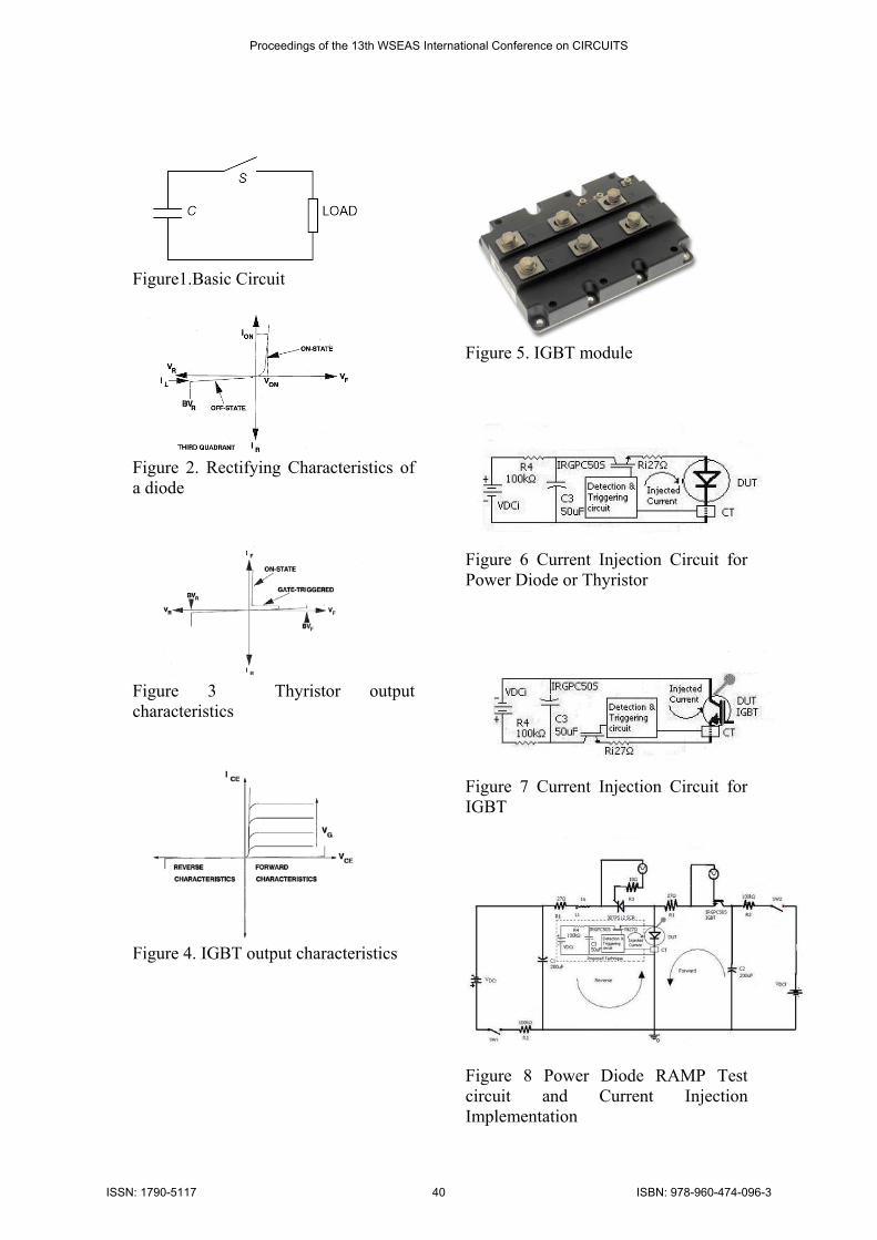
Figure1.Basic Circuit
Figure 2. Rectifying Characteristics of a diode
Figure 3 Thyristor output characteristics
Figure 4. IGBT output characteristics
Figure 5. IGBT module
Figure 6 Current Injection Circuit for Power Diode or Thyristor
Figure 7 Current Injection Circuit for IGBT
Figure 8 Power Diode RAMP Test circuit and Current Injection Implementation
Proceedings of the 13th WSEAS International Conference on CIRCUITS
ISSN: 1790-5117 40 ISBN: 978-960-474-096-3

Figure 9 Power Diode RAMP Test circuit Gate pulse
Figure 10 Anode current waveforms of power diode at reverse recovery
Figure 11 Thyristor RAMP Test circuit and Current Injection Implementation
Figure 12 Thyristor RAMP Test circuit Gate pulse
Figure 13 Anode current waveforms of Thyristor at reverse recovery
P+
Figure 14 : The carrier distribution in power diodes and thyristors
i
N+
Add St Ne
Proceedings of the 13th WSEAS International Conference on CIRCUITS
ISSN: 1790-5117 41 ISBN: 978-960-474-096-3
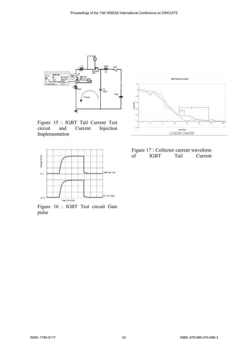
Figure 15 : IGBT Tail Current Test circuit and Current Injection Implementation
Figure 17 : Collector current waveform of IGBT Tail Current
Figure 16 : IGBT Test circuit Gate pulse
Proceedings of the 13th WSEAS International Conference on CIRCUITS
ISSN: 1790-5117 42 ISBN: 978-960-474-096-3