Vacuum Systems Electron Probe Microanalysis EPMA UW- Madison Geoscience 777 1/16/13.

EssentialKnowledgeBriefings
Electron probemicroanalysis
First Edition, 2015

ELECTRON PROBE MICROANALYSIS2
Front cover image: high-resolution X-ray maps of copper (Cu), zinc(Zn) and silver (Ag) illustrating the interdiffusion zone between themain material (Cu) and the brazing material (Ag-Zn). Data acquiredwith the SXFiveFE at 10keV, 30nA
© 2015 John Wiley & Sons Ltd, The Atrium, Southern Gate,Chichester, West Sussex PO19 8SQ, UKMicroscopy EKB Series Editor: Dr Julian HeathSpectroscopy and Separations EKB Series Editor: Nick Taylor

CONTENTS4 INTRODUCTION6 HISTORY AND BACKGROUND13 IN PRACTICE22 PROBLEMS AND SOLUTIONS28 WHAT’S NEXT?
ELECTRON PROBE MICROANALYSIS 3
About Essential Knowledge BriefingsEssential Knowledge Briefings, published by John Wiley & Sons,comprise a series of short guides to the latest techniques, appli -cations and equipment used in analytical science. Revised and updated annually, EKBs are an essential resource for scientists working in both academia and industry looking to update their understanding of key developments within each specialty. Free todownload in a range of electronic formats, the EKB range is availableat www.essentialknowledgebriefings.com

INTRODUCTIONElectron probe microanalysis (EPMA) is an analytical technique
that has stood the test of time. Not only is EPMA able to trace its originsback to the discovery of X-rays at the end of the nineteenth century,but the first commercial instrument appeared over 50 years ago. Nevertheless, EPMA remains a widely used technique for determiningthe elemental composition of solid specimens, able to produce mapsshowing the distribution of elements over the surface of a specimenwhile also accurately measuring their concentrations.
EPMA involves bombarding a specimen with a focused electron beam and analyzing the emitted X-rays. It generally combines two related analytical techniques – wavelength-dispersivespectroscopy and energy-dispersive spectroscopy (which is also thesubject of a separate Essential Knowledge Briefing) – in a single instrument known as a microprobe. Both techniques work by collecting characteristic X-rays and continuum released when thesurface of a specimen is bombarded with electrons. As their namessuggest, wavelength-dispersive spectroscopy separates emitted X-rays according to their wavelengths while energy-dispersive spectro scopy separates them according to their energies.
Wavelength-dispersive spectroscopy exhibits far better spectral resolution than energy-dispersive spectroscopy, but data collection is not as fast. When combined together in EPMA, energy-dispersive spectroscopy and wavelength-dispersive spec-troscopy complement each other to produce a powerful analyticalinstrument. Energy-dispersive spectroscopy can conduct a quickinitial analysis to identify the major elements, while wavelength-dispersive spectroscopy can perform a more detailed analysis toidentify trace elements and measure the concentrations accurately.
ELECTRON PROBE MICROANALYSIS4

EPMA has proved particularly adept at analyzing geological materials and metal alloys, able to reveal both the concentration andthe distribution of elements at the sub-micrometer scale. EPMA hasalso found use in a wide range of other applications, studying every-thing from the latest advanced solar cells to archaeological material.
This Essential Knowledge Briefing provides an introductionto EPMA and its capabilities. It begins with a detailed explanationof the operation of the instrument, including an explanation of whyelements emit characteristic X-rays, and outlines the major steps inthe development of EPMA over more than 100 years. It also detailsvarious practical issues related to the instrument, describes potentialproblems that may arise and how to solve them, and provides examples of how EPMA is being used by scientists in their research.Finally, it looks at prospective future applications and how the scientists developing these innovative applications will help to ensure that EPMA continues to stand the test of time.
ELECTRON PROBE MICROANALYSIS 5

HISTORY AND BACKGROUNDEPMA is a multi-faceted technique for determining the
concentration and the distribution of elements in solid specimens,from major elements to trace constituents. The EPMA techniqueinvolves bombarding a specimen with an electron beam and then analyzing the emitted X-rays with two different types of spectro meter, a wavelength-dispersive spectrometer (WDS) and an energy-dispersive spectrometer (EDS).
EPMA can identify and analyze all the elements of the periodictable, except for hydrogen and helium, in any solid material. Because the emission of X-rays is largely restricted to the area of thematerial exposed to the electron beam, EPMA can produce quanti-tative data on highly localized spots under 1µm in diameter. It has the additional benefit of being non-destructive, meaning thatquantitative measurements can be repeated as often as required.
The technique is routinely used to measure elements at trace levels of 100 parts per million (ppm). With optimized settings, modernEPMA devices can even measure elements at concentrations down toaround 10ppm. In addition to spot analyses, EPMA can also map elemental distributions over small or large areas. This is done by eitherscanning the beam across the surface of the specimen or moving thestage that holds the specimen in relation to a fixed beam.
EPMA utilizes an electron beam focused to a very narrow pointby magnetic lenses. When this beam hits an atom at the surface of asample, it can eject electrons from the atom’s inner high-energyshells (known as K, L and M shells), creating vacancies that are filledby electrons moving from the atom’s outer low-energy shells. Thismovement of electrons from outer to inner shells releases energy,which falls into the X-ray range of the electromagnetic spectrum.
ELECTRON PROBE MICROANALYSIS6

The energy of the emitted X-rays corresponds to the energy differ-ence between the shells involved in the transition. As every elementhas its own unique energy level spacing between shells, this processproduces characteristic X-ray emissions that can be used to identifythe element.
The origins of EPMA stretch back to the discovery of X-raysin 1895. Although first applied to medical fields, X-rays soon enteredthe fields of physics and chemistry. At Leeds University, UK,William Bragg and his son Lawrence were famed for their crystal-lography work using X-rays, which involved developing a criticallaw relating X-ray diffraction to crystal structure. In 1913, fellowphysicist Henry Moseley from the University of Oxford, UK, putBragg’s diffraction law to good use, building a spectrometer to measure the X-ray spectra of elements, based on their diffractionthrough crystals.
Moseley’s X-ray spectrometer used an X-ray tube, potassiumferrocyanide crystals and photographic plates. Moseley was able tobombard samples of available elements, measure the emitted wave-lengths and then determine the frequencies of the K and L lines inthe spectra (produced by electrons moving from lower energy shellsdown to the K and L shells). Importantly, he discovered that plottingthe square root of the frequency of the lines against a suitable integergave straight lines. The integer was revealed to be the atomic number, showing that the elements in any solid sample could beidentified by measuring the X-rays emitted. Although Moseley waskilled while fighting in World War I, his work had sown the seedsof an analytical revolution.
Meanwhile, developments in electron microscopy were alsopaving the way for EPMA. In 1932, the German company Siemens
ELECTRON PROBE MICROANALYSIS 7

built the first electron microscope. In 1944, James Hillier andRichard Baker at RCA Laboratories, Princeton, USA, filed a patentfor an ‘electronic microanalyzer’, which partnered an electron microscope with an energy-loss spectrometer and was able to analyze low atomic number elements. However, they never con-structed a working model and post-war communication difficultiesmeant their development was never widely publicized.
Then, in the late 1940s, Raimond Castaing, a research engineer atthe Office National d’Études et de Recherches Aéronautiques (ONERA),a French government research institution for aero nautical applica-tions, developed the first electron microprobe while studying for his PhD. ONERA had obtained two electron microscopes in 1947, andCastaing used the microscopes to investigate the X-rays emitted fromalloys bombarded by electrons. Castaing adapted one of the electronmicroscopes to turn it into a probe and used a Geiger counter to detectthe emitted X-rays, but found that he could not discriminate betweenelements using this technique. However, he cleverly resolved this issueby building and fitting a spectrometer incorporating a unique quartzcrystal to diffract particular wavelengths.
Castaing unveiled this novel technique at the First EuropeanConference on Electron Microscopy in 1950. Castaing’s PhD thesis,entitled Application des sondes électroniques à une méthode d’analyse
ponctuelle chimique et crystallographique (Application of electronprobes to a localized chemical and crystallographic analysismethod), was published in 1951. This thesis sparked worldwide interest in X-ray microanalysis, and much of the instrumentationand theory set out in it remain valid today.
In the years following Castaing’s thesis, ONERA built two proto -type electron microprobes, one of which was sent to the Institut
ELECTRON PROBE MICROANALYSIS8

de Recherches de la Sidérurgie, a French metallurgy research insti-tute. However, no patent was filed and industry was quick to see the commercial and analytical potential of the technique. Based onCastaing’s prototypes, the French company CAMECA (Compagniedes Applications Mécaniques et Électroniques au Cinéma et à l’Atomistique), a subsidiary of the Compagnie Générale de la Télégraphie sans Fil, was the first to produce a commercial EPMA,the MS85, in 1958. CAMECA still develops EPMA instrumentstoday – its latest model the SXFive was launched in 2011 (Figure 1).
As quantum entities, X-rays have characteristics of both par-ticles and waves and so can be detected by either their energies ortheir wavelengths, which is why EPMA instruments utilize bothEDS and WDS. For the EDS, EPMA instruments utilize silicon driftdetectors to measure the number of X-ray photons emitted at different energies. This gives a rapid semi-quantitative analysis andis mostly restricted to providing a quick identification of the majorelements present in a specimen.
In contrast to a single EDS, modern EPMA instruments typi-cally possess up to five WDSs, each of which is fitted with different
ELECTRON PROBE MICROANALYSIS 9
A B
Figure 1. (A) The MS85 – the first model of commercial EPMA. (B) The SXFive – CAMECA’slatest EPMA generation

diffracting crystals that reflect specific wavelengths. The multipleWDSs provide a more precise and accurate analysis, as they have theability to produce spectra with higher spectral resolution (5–10eVtypically) than EDS (120–130eV typically).
EPMA instruments also house an optical microscope for pinpointing the area of interest and three detectors for capturingthe cathodoluminescence (CL), secondary electrons (SE) and back -scattered electrons (BSE) that are also emitted from the specimenunder electron bombardment. These additional signals provide information on the specimen’s crystal structure, surface topographyand atomic weight.
Detectors for CL, which is the visible light generated when an electron beam impacts a luminescent sample, provide valuable information not easily generated by other means, especially relatingto crystal structure, highlighting trace impurities, lattice defects andcrystal distortion. For example, certain CL peaks arise from the energygap between the conduction band and the valence band in semi con -ductors, and so can be used to map strain and chemical composition.
For SE imaging, the electron microprobe effectively functionsas a scanning electron microscope, providing topographical information based on secondary electrons directly liberated fromtheir energy levels by the electron beam. These electrons have lowenergies and only those created within a few nanometers of the sample surface can escape; secondary electrons are therefore verysensitive to surface topography.
Images using BSEs show atomic number differences, based onthe fact that the number of BSEs increases with the increasing meanatomic number. In the resulting BSE image, brighter areas indicateheavier mean atomic number.
ELECTRON PROBE MICROANALYSIS10

The basic output of EPMA is a spectrum showing peaks thatrepresent X-rays with specific energies (EDS) or wavelengths (WDS),with each peak corresponding to a specific element. The lateral distribution of each element is obtained, by either beam or stagescanning, after acquiring X-ray maps at peak and off-peak (back-ground) positions. The sizes and proportions of phases identified in the analyzed material can be determined by combining severalX-ray maps (Figure 2).
ELECTRON PROBE MICROANALYSIS 11
Figure 2. X-ray maps acquired at high magnification on synthetic volcanic rockclearly reveal three phases: clinopyroxene (no K2O), glass (with 2% of K2O) andphlogopite (with 5% of K2O). Data courtesy of Ida di Carlo, Institut des Sciences de la Terre d’Orléans, France
10μm K2O 8keV 10μm MgO 8keV
10μm SiO2 8keV 10μm CaO 8keV
20.0
17.5
15.0
12.5
10.0
7.5
5.0
2.5
0.0
65.0
56.9
48.8
40.6
32.5
24.4
16.3
8.1
0.0
30.0
26.3
22.5
18.8
15.0
11.3
7.5
3.8
0.0
Ox% Ox%
Ox% Ox%
7.0
6.1
5.3
4.4
3.5
2.6
1.8
0.9
0.0

EPMA can also determine the concentration of the elementsbased on the intensities of the emitted X-rays, allowing it to conductabsolute quantitative analyses. This usually involves first collectinga spectrum with WDS and/or EDS to identify which elements arepresent in a specimen. Quantitative analysis is then performed usingjust the WDSs, by comparing the X-ray intensities measured for allthe elements identified in the initial spectral analysis against standards of known composition. After matrix correction for fluorescence, absorption and atomic number effect, the concentra-tions of all the elements identified in the specimen are accuratelydetermined. The results of quantitative EPMA analyses are commonly displayed as weight percentages of elements and/or oxides (Table 1).
This ability to conduct quantitative analyses is a majorstrength of WDS EPMA, which is recognized as the only non-destructive analytical technique able to provide absolute and accurate quantification for a specimen of interest. Using well-defined standards, it is possible to achieve quantitative analysis with an accuracy better than ±1%.
ELECTRON PROBE MICROANALYSIS12
Point Na2O K2O MgO CaO FeO Al2O3 SiO2 TiO2 H2O O=F Total1 0.430 5.097 16.324 0.124 11.885 14.285 46.081 1.364 4.287 0.006 99.8712 0.486 5.338 16.068 0.257 12.606 14.228 45.572 1.344 4.269 0.010 100.1583 0.581 6.918 18.908 0.283 12.647 13.681 41.821 1.107 4.182 0.003 100.1254 0.472 5.024 16.154 0.223 12.142 13.561 45.935 1.415 4.242 0.014 99.1555 0.492 4.836 16.924 0.522 12.622 13.253 46.717 1.181 4.305 0.016 100.8366 0.663 5.851 17.593 0.417 12.949 13.431 43.994 1.190 4.236 0.000 100.3247 0.466 5.640 15.805 0.461 12.957 14.095 44.938 1.217 4.241 0.006 99.8158 0.623 4.949 17.091 0.328 12.949 14.001 44.621 1.059 4.252 0.000 99.873
Numbers show the oxide weight percentage at a series of points in the sample.
Table 1. Quantitative compositional data for a synthetic volcanic rock at high temperature and high pressure. Data courtesy of Ida Di Carlo, Institut des Sciences de la Terre d’Orléans, France

IN PRACTICEThe EPMA configuration varies according to the user’s
requirements, but is always centered on an electron gun that firesbeams of electrons at the specimen. The electron gun is fitted to avacuum chamber equipped with a stage that can move the specimenin steps as small as one tenth of a micrometer, allowing the beam toexplore the entire specimen surface.
An optical microscope coaxial to the electron beam, and withcontinuously variable magnification, identifies the exact points ofinterest on the specimen surface. A charge-coupled device (CCD) camera allows samples to be viewed in reflected light and thin sectionsto be imaged in transmitted polarized light. Meanwhile, CL detectorsattached to the optical microscope port collect the visible light generated when the electron beam hits the specimen (Figure 3).
ELECTRON PROBE MICROANALYSIS 13
Electron sourceIon pumps
Optical zoom and CCD camera
Beam stabilizer
Reflecting objective
AirlockWDS
Diffracting crystals (1 to 4)
Specimen
Figure 3. Schematic of EPMA

Traditionally, the source of the electrons is a heated tungstenfilament or a lanthanum hexaboride (LaB6) cathode, which providesa high-intensity and small-diameter electron beam for high-resolution imaging. However, the implementation of the Schottkyemitter field-emission gun (FEG) on the EPMA electron column hastaken the technique to new analytical heights, improving the lateralresolution and performance at low accelerating voltages.
Analytical lateral resolution is a function of beam diameterand is related to the beam energy, beam current and sample density.Field-emission sources produce higher beam densities at lower energies than conventional LaB6 and tungsten sources. As a result,they generate narrower beams at higher currents, reducing the region over which scattered electrons generate X-rays, known as theinteraction volume, to sub-micrometer sizes. Not only does this improve analytical lateral resolution, it also reduces the contribu-tion of secondary fluorescence and decreases charging effects. In scanning electron microscopy mode, a FEG can pick out sample detailsthat are only ~3nm apart, compared with ~6nm for an LaB6 source and~7nm for tungsten.
The EDS collects the entire energy spectrum of the emitted X-rays simultaneously from all elements present in a sample. This qualitative information can be combined with informationcollected by the SE and BSE detectors. The EDS is used to identifythe major elements in a specimen, but can struggle to identify peaks from minor and trace elements. It produces spectra with quitebroad peaks, and peak overlap frequently occurs although this cangenerally be resolved by deconvoluting the peaks (Figure 4).
What really sets EPMA apart, though, is the series of WDSs,each of which measures a single wavelength at a time, making this
ELECTRON PROBE MICROANALYSIS14

system the ideal spectrometry tool for quantitative analysis of traceelements. Because the peak-to-background ratio achieved with theWDS is much better than for EDS, the minimum detection limitsfor WDS are at least 10 times lower than for EDS.
Each WDS may contain up to four diffracting crystals dedi-cated to a given range of X-ray wavelengths, with each WDS usingdifferent crystals to cover the entire X-ray spectrum. For example,lithium fluoride (LiF) crystals can detect lines from the K shell fora host of elements, from scandium to rubidium, as well as for L shelllines from tellurium to uranium. Other commonly used crystals include pentaerythritol (PET), thallium acid phthalate (TAP) andsynthetic multi-layered diffracting crystals (pseudo crystals).
ELECTRON PROBE MICROANALYSIS 15
EDS
WDSBa La
Inte
nsit
y (a
.u.)
Ti Ka
Ba Lb
Ti KbBa Lb2
Ba Lg
4.3 4.5 4.7 4.9 5.1 5.3 5.5Energy (keV)
Figure 4. The graph shows X-ray spectra of the same kinetic energy region taken withEDS and with WDS respectively. The order-of-magnitude difference in resolution isobvious, as is the value of higher resolution WDS over EDS in making unambiguousand accurate quantification

Low-energy (long-wavelength) X-rays require large lattice spacing in the crystals for diffraction. Multi-layered crystals are perfect for this purpose, as they maximize scattering efficiency topick up the wavelengths produced by the light elements (berylliumto fluorine).
The measured X-ray intensities, and thus the detection limits,are a function of the number of collected X-rays. Therefore, in order to increase the number of collected X-rays, diffracting crystals with larger surfaces have been developed. All diffractingcrystals are now available in larger sizes, allowing faster WDS analysis and improving minimum detection limits thanks to their high counting rates.
As WDS produces spectra with a greater peak-to-backgroundratio than EDS, it can detect trace elements that are lost in the back-ground noise with EDS. Because of this, EDS is often used to conductan initial survey of a sample, with WDS subsequently used to checkfor overlaps, hunt for trace elements and conduct quantitativeanalyses. Alternatively, some EPMA systems allow simultaneousacquisition of WDS and EDS data, with EDS searching for major elements and WDS targeting the trace constituents. Raw data produced by the EDS, WDS and other detectors are automaticallyacquired, processed and analyzed by software supplied with theEPMA, displaying the data as quantitative tables or as X-ray maps.The latest software packages can even combine the two to producequantitative maps of elemental distribution, increasing the instru-ment’s throughput efficiency.
This level of analytical capabilities allows researchers to useEPMA to study a wide variety of different materials, with particularemphasis on geological materials and metal alloys. EPMA can
ELECTRON PROBE MICROANALYSIS16

identify small intermediate phases, typically a few hundreds of nano meters in size, in geological materials such as metal ores, volcanic rocks and meteorites. It can also be used to date geologicalsamples containing monazite, which is found in many types of rock,as a complement to isotopic ratio measurements. Known as geo -chronology, this technique measures concentrations of uranium,thorium and lead, and is based on the fact that lead would not havebeen present at the time of monazite crystallization.
EPMA is regularly used to investigate the chemical structureof newly developed metal alloys and how this structure is altered in response to activities such as thermal processing and corrosion.But researchers also use it to study various other synthetic materials,such as glass and ceramics, as well as archaeological material like ancient pots and bronze artefacts. It has even been used to study various different types of natural material, including bone and soil.
ELECTRON PROBE MICROANALYSIS 17

ELECTRON PROBE MICROANALYSIS18
CASE STUDY 1 When the Icelandic volcano Eyjafjallajökull erupted in 2010,
teams from the University of Iceland and the University of Edin-
burgh, UK, were among the first to reach the scene. These teams were
keen to analyze the rapidly descending layers of volcanic ash, or tephra,
in order to understand the eruption, including its adverse effects on
air transport.1,2
Important within this research was the study of melt inclusions –
tiny pockets of magma, as small as 10µm across or less, trapped
within crystals that grow while the magma rises from its sources deep
in the Earth’s crust towards the volcanoes. The ascending magma
progressively releases volatile elements such as fluorine, chlorine and
sulfur, forming atmospherically damaging gases including hydrogen
fluoride and sulfur dioxide. Comparing volatile concentrations in
the earliest trapped inclusions – reflecting the original magma
composition – and the glass formed when the magma freezes upon
eruption – its final volatile content – allows estimates to be made of
the amount of gasses released. This can give an indication of the
environmental impacts of the eruptions.
Studying tephra involves using EPMA in ‘quite an unusual
way’, with extremely low beam currents, says Dr Chris Hayward at
the University of Edinburgh. This is because these glassy materials
can suffer chemical changes (principally loss of sodium) during
analysis, especially of small areas.
Hayward and his team have developed new EPMA methods
that allow them to carry out high-quality analyses of tephra layers that
were previously impossible. These high-resolution methods rely on
Edinburgh’s CAMECA instrument, which permits stable beam

currents down to 0.5nA and allows three separate beam currents
during a single analysis. Both these features are essential for conduct-
ing measurements at the small beam size (3µm) required to ensure
that sodium and potassium are kept within the analysis volume.
1. Hayward C. High spatial resolution electron probe microanalysis of tephras
and melt inclusions without beam-induced chemical modification. Holocene
2012;22:119–25. (http://dx.doi.org/10.1177/0959683611409777)
2. Gudmundsson MT, Thoordarson T, Hoskuldsson A, et al. Ash generation
and distribution from the April–May 2010 eruption of Eyjafjallajökull,
Iceland. Sci Rep 2012;2:572. (http://dx.doi.org/10.1038/srep00572)
SiO2 TiO2 Al2O3 FeO MnO MgO CaO Na2O K2O P2O5 TotalAv (wt%) 62.06 0.25 18.11 4.49 0.14 0.12 1.07 8.34 5.41 0.03 100.041σ St Dev 0.81 0.01 0.62 0.30 0.02 0.03 0.09 0.72 0.22 0.01
Det Lim 100 238 261 532 88(ppm)
Av, average; St Dev, standard deviation; Det Lim, detection limits.
ELECTRON PROBE MICROANALYSIS 19
Quantitative EPMA data for Mount Edziza sheep-track tephra with 3µm beam diameter (average of 27 points)
Melt inclusions (rounded blueareas) within a plagioclasecrystal from a tephra grainerupted by Eyjafjallajökull in 2010, Iceland. The X-raymap shows the concentrationof calcium within the crystaland the glass. Surrounding the crystal is glass frommagma quenched during the eruption. Image courtesy of Chris Hayward
13.9
12.9
11.9
10.9
9.9
8.9
7.9
6.9
5.9500μm Ca 15keV
wt%
ELECTRON PROBE MICROANALYSIS20
CASE STUDY 2Metal alloys are the main focus of the EPMA studies
con ducted by Dr Eric Leroy at the Institute of Chemistry and
Materials Paris-East in France. ‘In my laboratory, we synthesize
different types of metallic alloys: rare earth, aluminium or different
types of intermetallics,’ he explains. ‘The main purpose of my analyses
is to obtain the microstructure of the samples and the compositions
of the phases.’
These new metallic alloys are becoming increasingly complex,
made up of many different metallic elements at similar concentrations
rather than just one or two major elements and a few minor ones.
In a recent study, Leroy used EPMA to investigate how the micro -
structure of a high-entropy alloy comprising chromium, manganese,
iron, cobalt and nickel responded to thermal processing. He has also
used EPMA to optimize the properties of intermetallic magnesium-
lead-copper (MgPdCu) alloys that are essential for hydrogen storage
in new battery research and development.1
‘The major information obtained by EPMA is the precise
chemical composition and the X-ray maps,’ says Leroy. ‘Sometimes
I also use EPMA for the characterization of multi-layered samples;
in this case, the information wanted is thickness and the composition
of the layers.’
But Leroy hasn’t entirely restricted his use of EPMA to
metallic alloys. For example, he has used it to determine the chemical
composition and microstructure of grains in a sediment core taken
from a swamp in the Pacific islands of Vanuatu.2 This helped to
reveal how the environmental conditions on the islands have changed
over the past 6500 years. He has also used EPMA to study how the

ELECTRON PROBE MICROANALYSIS 21
long-term use of self-cleaning glass affects its chemical composition,
particularly whether the outer coating of titanium dioxide is prone
to leaching away.3
1. Ponthieu M, Fernández JF, Cuevas F, et al. Thermodynamics and reaction
pathways of hydrogen sorption in Mg6(Pd,TM) (TM = Ag, Cu and Ni)
pseudo-binary compounds. Int J Hydrogen Energy 2014;39:18291–301.
(http://dx.doi.org/10.1016/j.ijhydene.2014.09.034)
2. Wirrmann D, Eagar SH, Harper MA, et al. First insights into mid-
Holocene environmental change in central Vanuatu inferred from a terrestrial
record from Emaotfer Swamp, Efaté Island. Quat Sci Rev 2011;30:3908–24.
(http://dx.doi.org/10.1016/j.quascirev.2011.10.003)
3. Chabas A, Alfaro S, Lombardo T, et al. Long term exposure of self-cleaning
and reference glass in an urban environment: a comparative assessment. Build
Env 2014;79:57–65. (http://dx.doi.org/10.1016/j.buildenv.2014.05.002)
Copper precipitates in an Mg-Pd matrix. The high-resolution X-ray maps illustratethe microstructure and the composition of the phases in this ternary alloy
16
14
12
10
8
6
4
2
010μm PdLa 6keV
32
28
24
20
16
12
8
4
010μm CuLa 6keV
124
110
96
82
68
54
40
26
1210μm MgKa EDS 6keV
cts
cts cts10μm BSEZ 6keV

PROBLEMS AND SOLUTIONSAs with any analytical technique, EPMA does have some
limitations and restrictions. It cannot identify hydrogen or heliumin specimens, due to the fact that hydrogen and helium atoms only possess electrons at one energy level. This means EPMA is notoptimal for analyzing hydrous minerals.
Also like other analytical techniques, to get the most out of EPMA, users need to optimize operating conditions for their own particular specimen, instrument configuration and analytical requirements. For example, the specimen needs to be clean, flat andfinely polished. Surface imperfections can interfere with electron-sample interactions and make experimental set-up trickier, requir-ing carefully selected angles for the spectrometers. When mountedin a vertical position, orthogonal to the surface of the specimen,WDS is highly sensitive to sample roughness and positioning. Sample roughness and wrong positioning can lead to a loss of up to70% of the emitted X-rays. This can be resolved by tilting the WDS,as an inclined WDS is far less sensitive to the X-ray source position,and then using the optical microscope to line up the WDS on the specimen.
Electrically insulating specimens need to be coated with a thin film of a conducting material such as carbon to minimize thecharging effects and to reduce specimen heating. Failure to coat samples will lead to them becoming electrically charged, making themimpossible to analyze. Once the specimen has been loaded onto thestage, the sample chamber is pumped to high vacuum (10–5–10–6 Pa) to prevent gas and vapour molecules from interfering with the electron beam. The accelerating voltage and electron beam currentthen need to be carefully selected and the electron beam focused.
ELECTRON PROBE MICROANALYSIS22

Critical electron beam parametersAccelerating voltage and beam diameter are the two most
important parameters to optimize for quantitative X-ray analysis.Optimum conditions are obtained when the analytical spatial resolution is primarily limited to the diameter of the X-ray emissionvolume in a specific material.
FEGs can produce extremely small diameter and bright beams especially at low beam voltages (100nm @ 10keV and 10nA).This is a great advantage for high lateral resolution analyses, as low beam voltages reduce the diameter of the X-ray emission volume. However, low beam voltages can only excite low-energy X-rays (K lines for elements with an atomic number below 22, andL and M lines for elements with higher atomic numbers). For quantification, the use of low-energy X-rays is also challenging asthey are subject to larger peak shifts, more peak interferences andlower fluorescence yields compared to higher energy K lines. Peakinterferences can be resolved using specific software, and accurate
ELECTRON PROBE MICROANALYSIS 23
Inte
nsit
y (a
.u.)
1.00
0.80
0.60
0.40
0.20
0.000.81 0.82 0.83 0.84 0.85 0.86 0.87 0.88 0.89
Energy (keV)
Lα
LIII absorption edge
Lα3
Lα4
Lα5Lβ
LII absorption edge
Lβ‘1Lβ”1
Figure 5. Ni La Lb spectral range in pure nickel acquired at 5keV (blue), 10keV (green)and 15keV (red) revealing modification in shape and peak positions

quantification with low-energy X-rays can be achieved by using Ll lines (Figures 5 and 6, and see Case Study 3).
Challenges specific to quantitative analysisThe parameters that are important to optimize when conduct-
ing trace analysis include beam conditions, spectral conditions (energy resolution, background positions, interferences) and analysis time. Trace analysis at the highest levels of sensitivity requires both high beam energies and high beam currents (in therange of 100nA to 200nA) to produce as many X-ray counts as possible for the element of interest. These parameters are easily accessible through dedicated EPMA software.
For any quantitative analyses, the quality of the data depends on beam current stability and on the reproducibility,sensitivity and spectral resolution of the WDS. For example, with an optimized tungsten filament EPMA system, beam stability of ±0.05% per hour can be achieved using permanentbeam regulation.
ELECTRON PROBE MICROANALYSIS24In
tens
ity
(a.u
.)
0.40
0.20
0.00
0.60 0.61 0.62 0.63Energy (keV)
Mg Ka2nd order+ Fe Lh
Fe Ll
Figure 6. Fe Ll spectral range in pure iron (green), haematite (red), and almandine(blue) allowing accurate quantification of the first series transition metals
Both trace and quantitative analyses with EPMA are relianton the multiple WDS to provide data with greater spectral resolution and a greater peak-to-background ratio than EDS. Nevertheless, WDS peaks still need to be separated from a back-ground of con tinuum radiation resulting from inelastic collisionsby incident electrons in the specimen. The solution involves calculating background intensities at spectral peak positions by interpolating between count rate measurements on both sides of the peaks.
ELECTRON PROBE MICROANALYSIS 25
ELECTRON PROBE MICROANALYSIS26
CASE STUDY 3Dr John Fournelle at the University of Wisconsin, Madison,
USA, has used field-emission EPMA to analyze samples of lunar
surface deposits (regolith grains) collected during an Apollo mission.
These scarce iron-silicon (Fe-Si) grains are thought to have formed
in the reducing environment of the moon after micrometeorite
impacts, perhaps affected by solar wind.
Making matters difficult is the fact that the Fe-Si compounds
of interest are under one micrometer in diameter, requiring a highly
focused, low-voltage electron beam. Before the advent of field-emission
sources, there was little research interest in quantitative low-voltage
EPMA because the electron beam simply could not be focused to
sufficiently small diameters. Also, the related lower electron beam
energies mean that many of the inner shell electrons generally used
in EPMA cannot be ionized. Because surface contamination can
negatively impact results at low voltages, electron probes with oil-free
vacuum systems are essential, as well as anti-contamination devices.
Armed with a field-emission probe, however, Fournelle and his
team were keen to measure previously poorly studied L shell X-ray
lines in the lunar Fe-Si samples, taking advantage of a sub-micrometer
beam focusing at low keV. Whereas EPMA normally uses a
15–20keV beam, Fournelle’s team was able to use a 5keV beam. ‘We
quickly found, however, that using the Fe La or Lb lines produced
incorrect compositions in the reference materials we started experi-
menting with, before we turned the electron beam loose on the
sub-micron lunar grains,’ he says.
The researchers discovered that a normally ignored, non-
traditional X-ray line, the Fe Ll line, isn’t impacted by the complex

ELECTRON PROBE MICROANALYSIS 27
phenomenon of self-absorption that affects the Fe La and Lb lines,
and thus could produce excellent EPMA results.1 When Fournelle
and his team conducted their original work, no commercial software
was available to acquire and process the Fe Ll lines. ‘We have been
working together with CAMECA, and they have quickly grasped the
importance of these non-traditional lines for low-voltage EPMA and
have now implemented the utilization of the Ll lines in their calibra-
tion, measurement and quantification software,’ Fournelle explains.
His next objective is to use ‘non-traditional’ M lines for low-voltage
EPMA of rare earth elements, a hot topic in both geoscience and
materials research.
1. Gopon P, Fournelle J, Sobol PE, Llovet X. Low-voltage electron-probe
microanalysis of Fe–Si compounds using soft X-rays. Microsc Microanal
2013;19:1698–708. (http://dx.doi.org/10.1017/S1431927613012695)
WHAT’S NEXT?As highlighted in the History and Background chapter, EPMA
is not a new analytical technique, with the first commercial system introduced in 1958. Although the underlying technology has improved greatly since then, the basic principles of EPMA are exactly the same. So why does EPMA remain such a popular and commonly used analytical technique after more than half a century?
The main reason is that it is still the only non-destructive analytical technique that can accurately determine the concentra-tion of almost any element in almost any solid material, whethercrystalline or amorphous. This inherent ability has recently beenenhanced by the improved resolution offered by new electron beamsources such as FEG and the ease of use provided by the latest software tools. Nevertheless, there is still a certain amount of roomfor improvement.
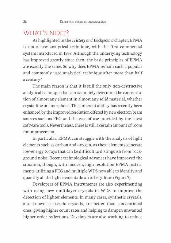
In particular, EPMA can struggle with the analysis of light elements such as carbon and oxygen, as these elements generate low-energy X-rays that can be difficult to distinguish from back-ground noise. Recent technological advances have improved the situation, though, with modern, high-resolution EPMA instru-ments utilizing a FEG and multiple WDS now able to identify andquantify all the light elements down to beryllium (Figure 7).
Developers of EPMA instruments are also experimenting with using new multilayer crystals in WDS to improve the detection of lighter elements. In many cases, synthetic crystals, also known as pseudo crystals, are better than conventional ones, giving higher count rates and helping to dampen unwanted higher order reflections. Developers are also working to reduce
ELECTRON PROBE MICROANALYSIS28
the time it takes to collect WDS spectra, by for example using multichannel analyzers.
The range of materials that EPMA is being used to examine is also expanding all the time, as new materials are continually developed. For example, over the past few years scientists have used EPMA to study the distribution of silver nanoparticles on titanium oxide nanotubes and the composition of solar cells madefrom thin films of copper, tin and sulfur (see Case Study 4 for another example).
ELECTRON PROBE MICROANALYSIS 29
20μm BSEZ 10keV
1000
900
800
700
600
500
400
300
20020μm AlKa 10keV
192
168
144
120
96
72
48
24
020μm OKa 10keV
80
70
60
50
40
30
20
10
020μm ZrLa 10keV
Figure 7. High-magnification X-ray maps acquired on a ceramic specimen illustratingthe ability of FEG-EPMA to analyze light elements (oxygen in this case) in a complexceramic matrix also containing zirconium and aluminium
cts
ctscts

ELECTRON PROBE MICROANALYSIS30
CASE STUDY 4 ‘We use EPMA for non-standard things,’ says Professor
Robert Martin, a physicist at the University of Strathclyde, Glasgow,
UK. His team specializes in the light-emitting semiconductors used
in lasers and light-emitting diodes (LEDs), and has recently developed
a novel EPMA-based approach for studying LEDs in situ.
The team originally had to use different instruments to measure
semiconductor composition and light emission. ‘We realized that the
microprobe allowed you to do both together on a very small region of
a sample,’ recalls Martin. Using EPMA, they can now map semi-
conductors with sub-micrometer scale resolution, simultaneously
measuring optical emission spectra and X-ray spectra for elements
such as the all-important indium and gallium.1
Martin’s team uses a CAMECA EPMA, which it has
customized by adding its own CL system. The physicists map
composition and optical properties and then look for correlations
between the two, for example whether the emission becomes brighter
with higher concentrations of a particular element.
In addition, Martin’s team has added electron-beam induced
current (EBIC) mapping into the mix, allowing them to study semi-
conductor conductivity at the same time as its elemental composition
and optical properties. The electrons and holes generated by electron
beam excitation are used to generate conductivity maps, showing how
well the charge flows to an external circuit such as that formed using
the contacts on an LED.
The physicists originally used EPMA to study specific layers
in LEDs, but they have recently taken their approach to new levels
by examining finished devices under operation. ‘We realized that
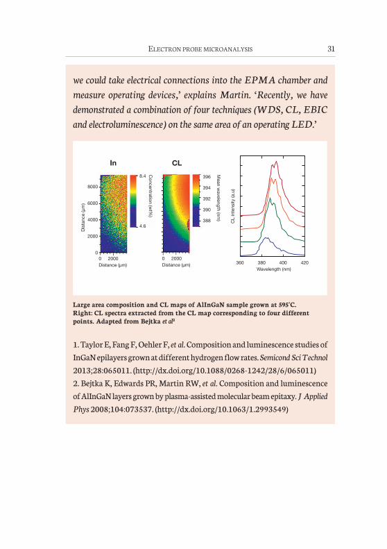
ELECTRON PROBE MICROANALYSIS 31
we could take electrical connections into the EPMA chamber and
measure operating devices,’ explains Martin. ‘Recently, we have
demonstrated a combination of four techniques (WDS, CL, EBIC
and electroluminescence) on the same area of an operating LED.’
1. Taylor E, Fang F, Oehler F, et al. Composition and luminescence studies of
InGaN epilayers grown at different hydrogen flow rates. Semicond Sci Technol
2013;28:065011. (http://dx.doi.org/10.1088/0268-1242/28/6/065011)
2. Bejtka K, Edwards PR, Martin RW, et al. Composition and luminescence
of AlInGaN layers grown by plasma-assisted molecular beam epitaxy. J Applied
Phys 2008;104:073537. (http://dx.doi.org/10.1063/1.2993549)
Large area composition and CL maps of AlInGaN sample grown at 595°C. Right: CL spectra extracted from the CL map corresponding to four differentpoints. Adapted from Bejtka et al2
8000
6000
4000
2000
0
In CL
Dist
ance
(μm
)
0 2000Distance (μm)
0 2000Distance (μm)
396
394
392
390
388
Mean wavelength (nm
) CL in
tens
ity (a
.u)
360 380 400 420Wavelength (nm)
8.4
4.6
Concentration (wt%)

ConclusionWith its unique ability to identify and quantify elements in
solid samples with great sensitivity and high accuracy, EPMA hasbeen at the forefront of analytical technology for over 50 years. Asthe analytical demands of scientists have increased and the range ofmaterials they want to study has grown, EPMA has managed to stayrelevant. This is partly because of the inherent advantages of thetechnology, which were apparent from the very beginning, andpartly because of the advances that have occurred over the past 50 years, such as high-resolution electron beams and sophisticatedsoftware. With no sign that the ability to identify and quantify elements in solid samples will become any less useful or valuable in the future, EPMA’s position is probably secure for at least thenext 50 years as well.
ELECTRON PROBE MICROANALYSIS32

FURTHER INFORMATIONCAMECA website. (http://www.cameca.com/literature/scientific-
publications/epma.aspx)Castaing R. Application of electron probes to local chemical
and crystallographic analysis. PhD Thesis, University of Paris, 1951English translation by Duwez P and Wittry DB , California Instituteof Technology, 1955. (http://www.microbeamanalysis.org/history/Castaing-Thesis-clearscan.pdf)
Goldstein J, Newbury DE, Joy DC, et al. Scanning electron
microscopy and X-ray microanalysis, 3rd edn. New York: Springer,2003. (http://dx.doi.org/10.1007/978-1-4615-0215-9)
Holton I. Is energy-dispersive spectroscopy in the SEM a substitute for electron probe microanalysis? Micros Anal 2012;26:S4–7.(http://www.microscopy-analysis.com/sites/default/files/magazine_pdfs/magazine%202012_May_Holton.pdf)
Hombourger C, Outrequin M. Quantitative analysis and high-resolution X-ray mapping with a field emission electron microprobe. Micros Today2013;21:10–5. (http://dx.doi.org/10.1017/S1551929513000515)
ELECTRON PROBE MICROANALYSIS 33

EssentialKnowledgeBriefings