Electron microscopy Peter Nagy ([email protected] ... · Scanning transmission electron...
47
1/47 Electron microscopy Peter Nagy ([email protected]) Department of Biophysics and Cell Biology, University of Debrecen
Transcript of Electron microscopy Peter Nagy ([email protected] ... · Scanning transmission electron...

1/47
Electron microscopy
Peter Nagy ([email protected])
Department of Biophysics and Cell Biology, University of Debrecen
2/47
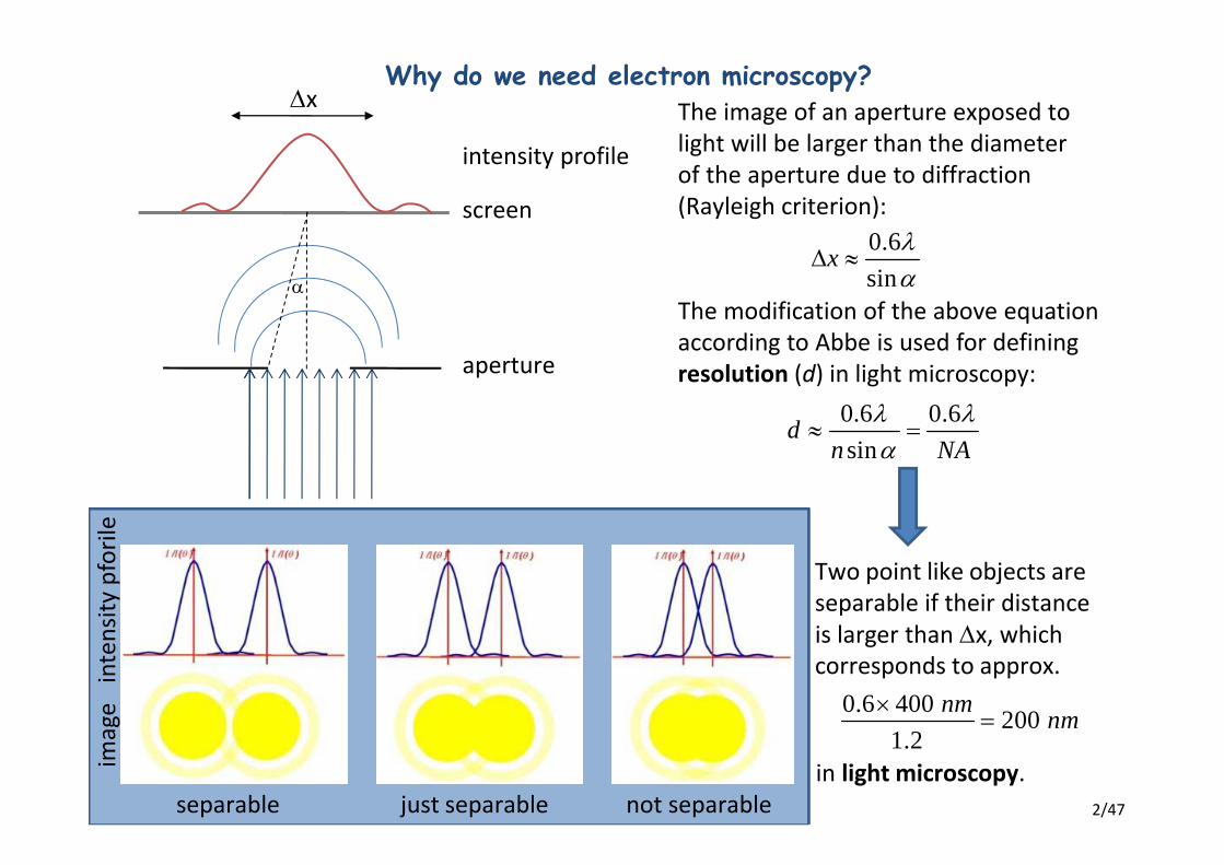
Why do we need electron microscopy?
aperture
screen
intensity profile
The image of an aperture exposed to light will be larger than the diameter of the aperture due to diffraction(Rayleigh criterion):
x
0.6sin
x
The modification of the above equation according to Abbe is used for defining resolution (d) in light microscopy:
0.6 0.6sin
dn NA
Two point like objects are separable if their distance is larger than x, which corresponds to approx.
imag
ein
tens
ity p
foril
e
separable just separable not separable
0.6 400 200 1.2
nm nm
in light microscopy.

3/47
Why do we need electron microscopy?
The resolution of conventional light microscopy cannot significantly exceed, i.e. be lower than 200 nm.
0.6 0.6sin
dn NA
several technical obstacles prevent us from using
wavelengths below 400 nm:
• in the UV range special lenses are required, and this
modification results in a max. 2-fold improvement in
resolution
• radiation with even lower wavelength (X-ray) cannot
be focused with lenses
o special Fresnel zone plates (diffraction plates)
are required for focusing X-rays
o generation of X-rays and construction of an X-ray
microscope are costly
Numerical aperture
cannot significantly
increase beyond 1.

4/47
According to Louis de Broglie, a French physicist, a wave can be assigned to each elementary particle whose wavelength is given by the following equation:
Why do we need electron microscopy?
hp
2
cE hf h
E mc
2c h hh mc mc p
Einstein’s equationmomentum of the photon(p=mv)
Derivation of the de Broglie equation from the quantum theory of light and from Einstein’s thoery of special relativity:
According to the de Broglie equation the wavelength assigned to an elementary particle is inversely proportional to the momentum of the particle: fast particle short wavelengthKinetic energy of an electron accelerated in an electric field: kinE eU
221
2 2kinpE mvm
2 2kinp mE meU
Wavelength of an accelerated electron:
1.23 nm2
h hp meU U
Sub-nanometer wavelength
and resolution can be achieved using small acceleration voltages.

5/47
Physical resolution of an electron microscope
1.23 nm
0.6 sin
U
dn a
0.6 1.23 0.74 nm sin
dn U U
The half angle of lenses in electron microscopes is small, 0.01 rad.The index of refraction is 1.
Therefore, the resolution at an accelerating voltage of 10000 V is:
0.74 0.74 nm0.01 10000
d

6/47
Types of electron microscopes
Transmission electron microscope (TEM)
electron gun
condenser lens
sample
objective lens
projection lens
screen
electron gun
condenser lens
objective lens
scanning coils
secondary electron detector
sample
X-ray detector
Scanning electron microscope (SEM)
The sample is imaged at once, similar to a conventional light microscope, but electrostatic or magnetic lenses are used instead of optical lensesl.
X-rays or secondary electrons induced from single pixels of the sample are detected followed by scanning across the whole sample.
Scanning transmission electron microscope (STEM)
Mixture of SEM and TEM:• scans pixelwise• but detects transmitted
radiation

7/47
Comparison of electron and light microscopes
condenser
sample
objective
ocular or projection
lens
light or electron source
fluorescent screen
condenser 1
condenser 2
condenser 3
sample
detector
secondaryelectrons
light microscope TEM SEM
acceleration of electrons in an
electric field

8/47
The electron gun
• thermionic emission: electrons are emitted from a heated wire (filament).
o due to the negatively charged Wehnelt cylinder electrons are only emitted from the tip of the wire the electron beam is easier to focus.
o The filement can be made of tungsten or LaB6. Filaments made of LaB6 generate stronger currents (more electrons).
• Schottky emission: the magnitude of thermionic emission increases if the filament is negatively charged the filament must be heated to a lower temperature.
o filaments for Schottky emission are usually made of tungsten covered by zirconium-oxide.
• field emission: if the negative voltage applied to the cathode is large enough, electrons are emitted from it even without heating as a result of quantum mechanical tunneling. Field emission cathodes are made of tungsten.
U
Wehnelt filament(cathode)
0
Epot
pot. energy of the e- at small
and large U
the potential energy of the e-
as a result of the positive charge left behind
the resultant potential
energy of the e-
at small and large U
if this distance is small, quantum
mechanical tunneling can be
observed
electrode vacuum

9/47
Acceleration of electronsElectrons are accelerate to high speeds as a result of large voltages.
According to the work-energy theorem the work done by the electric field (eU) increases the
kinetic energy of the electron:2
012
eU m v
Since the speed of electrons approaches the speed of light, the relativistic equation must be
used instead of the above one, which takes the increase of the mass of the electron into
account:2
2002 2
2 2
1, =1 1
m ceU eU m cv v
c c
e – charge of electron, U – accelerating voltage, m0 – rest mass of electron, v – velocity of electron
c – speed of light – relative increase in mass
U (kV) or E0 (keV) v/c 1/2m0v2 (keV)
100 1.2 0.55 77
200 1.39 0.7 124
300 1.59 0.78 154
1000 2.96 0.94 226
The largest fraction of the energy is
used for increasing the mass.

10/47
Electron optics
1. Electrostatic lens:circle-shaped, negatively charged electrons with a cavity in the middle, which deflect the electrons toward the middle.
2. Magnetic lens: The magnetic field is generated by coils. The direction of magnetic Lorentz force is perpendicular to both the magnetic field and the velocity of the particle:
Brvz
• the direction of the magnetic field is mainly radial• the direction of the velocity is mainly parallel to the axis
of the coil (z direction)
the direction perpendicular to both directions is tangential the electron will be deflected tangentially.
• the direction of the magnetic field is mainly along the z axis• the magnetic Lorentz force does not act on the z component
of the velocity (sin =0), but the velocity has a tangential component as well
sinF Bqv the radial direction is perpendicular to both the magnetic field directed along the z axis and the tangential component of the velocity the electron is accelerated toward the middle of the coil
at
vz
ar
Bz
vt

11/47
Imaging aberrations
Images generated by electron lenses do not meet all the requirements of perfect imaging, similar
to optical lenses:
1. A single image point corresponds to a single object point.
2. The pattern of image points shall be similar to the pattern of object points.
3. The focal length of the objective shall not be dependent on the distance.
The most important imaging aberrations of electron lenses:
1. Spherical aberration: electrons at different distances from the axis are focused to different
points.
focal length for electrons far from the axis
focal length for electrons close to the axis (f)
2 3 3s sr cf a C a
rs
1. Spherical aberration is proportional to the cube of the half angle of the lens().
2. The stronger the lens (small f), the smaller spherical aberration is.
3. The focal length can be decreased by increasing the lens current.
12/47
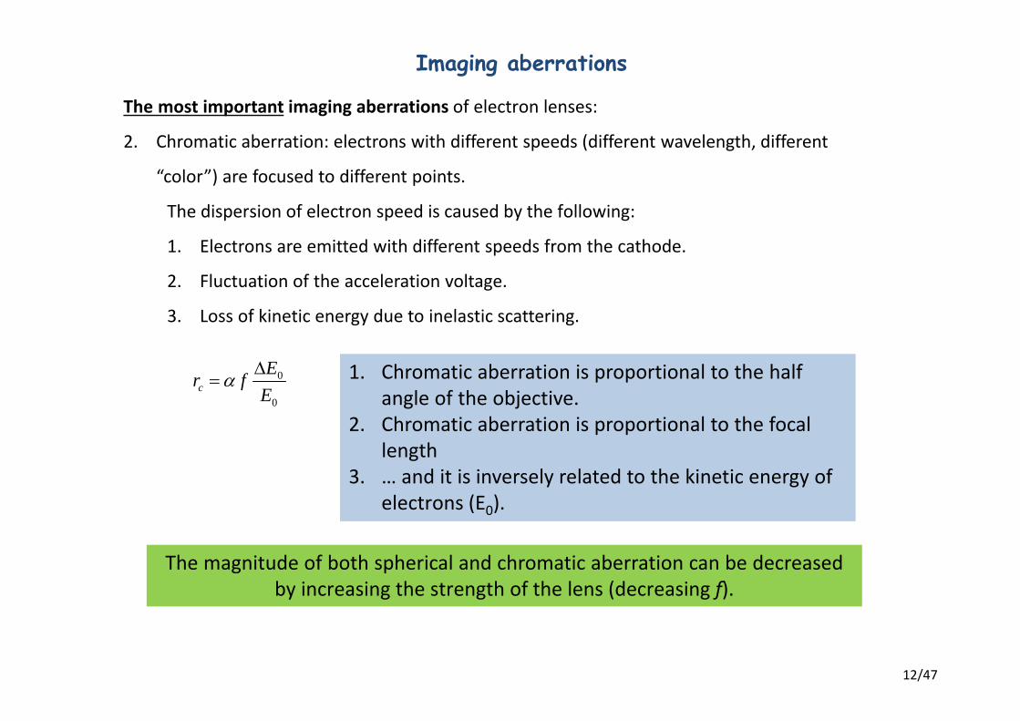
The most important imaging aberrations of electron lenses:
2. Chromatic aberration: electrons with different speeds (different wavelength, different
“color”) are focused to different points.
The dispersion of electron speed is caused by the following:
1. Electrons are emitted with different speeds from the cathode.
2. Fluctuation of the acceleration voltage.
3. Loss of kinetic energy due to inelastic scattering.
Imaging aberrations
0
0c
Er fE
1. Chromatic aberration is proportional to the half angle of the objective.
2. Chromatic aberration is proportional to the focal length
3. … and it is inversely related to the kinetic energy of electrons (E0).
The magnitude of both spherical and chromatic aberration can be decreased by increasing the strength of the lens (decreasing f).

13/47
Imaging aberrations
The imaging aberration typical of magnetic lenses is image rotation.
Image rotation is the consequence of the tangential acceleration of electrons entering the coil.
object points
image pointsimage points corresponding to the true location of object points

14/47
Comparison of electrostatic and magnetic lenses
Advantages of electrostatic lenses Advantages of magnetic lenses
No image rotation Imaging aberrations are less significant
Low energy requirement, simple No need for high voltage
No need for a very stable power source
They can be applied as immersion lenses
Ions can also be focused
Electron lenses have a large depth of field, i.e. layers at different distances from the lens are in focus.

15/47
Vacuum
In an electron microscope, especially in a TEM, vacuum must be generated in order to prevent• scattering of electrons• discharges between high-voltage components.
Oil evaporates followed by its downward flow due to the downward air stream. Oil particles deflect gas molecules downward due to their collision. Therefore, the concentration of gas molecules decreases in the top part. Oil is condensed as a result of collision with the cold wall of the pump.
Rotation of the piston with an eccentric axis of rotation sucks air in (blue arrow), compresses it (green arrow) followed by pumping it out (red arrow).
Methods and tools for generating vacuum:1. Rotary vane pump 2. Diffusion pump

16/47
Vacuum
Methods and tools for generating vacuum:3. Turbomolecular pump
High-speed turbineDischarges between electrodes ionize gas molecules and ionized gas particles collide into the electrodes.
4. Ion pump

17/47
Interaction of electrons with the sample in TEM
sampleaccelerated electrons
+-
-
--
-
-
diameter of a nucleus~ 10-15 m
diameter of an atom~ 10-10 m
scattering due to the attraction of the nucleus
-
-szóródás külső (lazán kötött) elektronokon
scattering angle() ~ (b – impact parameter) 1b
b
Ekin,0
Ekin,1A
Ekin,1B
,0
since
kin electronnucleus electron
kin scatterer
E mM m
E M
inelastic scattering
elastic scattering(elastic Ekin ~ 0)
1P inelasticP elastic Z
In the case of heavy nuclei (large Z) elastic scattering dominates
hfvvmEE electronelectronelectronAkinkin 21,
20,1,0, 2
1
The kinetic energy of elastically scattered electrons do change, since an electron undergoing centripetal
acceleration will emit electromagnetic radiation (photon).
photon (hf)

18/47
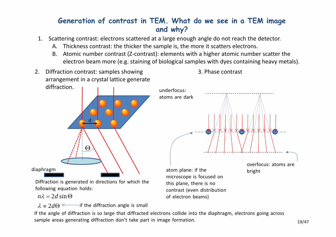
Generation of contrast in TEM. What do we see in a TEM image and why?
In a light microscope (not phase or interference contrast) mainly absorption is responsible for contrast generation:
image
electron scattering part („electrone-dense”)
lens
es
sample
Electrons are not absorbed, but scattered in the sample in an electron microscope. In TEM the most important contrast generating mechanism of scattering (scattering contrast).
light absorbing part of the sample
image
electrons scattered by electron-dense parts of the sample collide into the diaphragm and are therefore excluded from image formation
lens
es
diaphragm
19/47
Generation of contrast in TEM. What do we see in a TEM image and why?
1. Scattering contrast: electrons scattered at a large enough angle do not reach the detector.A. Thickness contrast: the thicker the sample is, the more it scatters electrons.B. Atomic number contrast (Z-contrast): elements with a higher atomic number scatter the
electron beam more (e.g. staining of biological samples with dyes containing heavy metals).
Diffraction is generated in directions for which the following equation holds:
2 sin2
n dd
if the diffraction angle is small
If the angle of diffraction is so large that diffracted electrons collide into the diaphragm, electrons going across sample areas generating diffraction don’t take part in image formation.
3. Phase contrast
atom plane: if the microscope is focused on this plane, there is no contrast (even distribution of electron beams)
underfocus: atoms are dark
overfocus: atoms are bright
2. Diffraction contrast: samples showing arrangement in a crystal lattice generate diffraction.
diaphragm
d

20/47
Electron diffraction
• It is not identical to diffraction contrast appearing in TEM images.
• It can be seen when the lens system of the TEM is adjusted such that the diffraction pattern
generated in the back focal plane of the objective is projected on the screen.
Image showing electron diffraction
• The structure of crystalline material can be calculated from the electron diffraction image.
• Electron diffraction is based on the same principle as X-ray diffraction, but the latter is more accurate.

21/47
Sample preparation for transmission electron microscopyFor biological samples
• sample preparation may be the longest part of the electron microscopic experiment
• sample preparation has a larger impact on the achievable resolution than the physical parameters of the electron microscope (sub-nanometer resolution can theoretically be achieved with electron microscopy, but this is hardly ever possible with biological samples)
• the aim of biological sample preparation is the generation of ultra-thin samples transparent for electron beams
• contrast enhancement with stains containing heavy metalsSteps of biological sample preparation:
1. Fixation: with glutaraldehyde in most cases
2. Dehydration: water is removed by placing the sample into a series of increasing ethanol or acetone concentrations. Dehydration is required because water would quickly evaporate in the vacuum of TEM damaging the sample. In addition, epoxy resin is hydrophobic, and it can penetrate the sample if water is removed.
3. Embedding: Samples are impregnated by epoxy resin so as to make them solid for cutting.
Samples embedded into epoxy resin.

22/47
Sample preparation for transmission electron microscopy
Steps of biological sample preparation:
4. Cutting with an ultramicrotome: a glass or a diamond blade cuts slices of 100 nm thickness,
which are allowed to swim on the surface of water.
23/47
Sample preparation for transmission electron microscopy
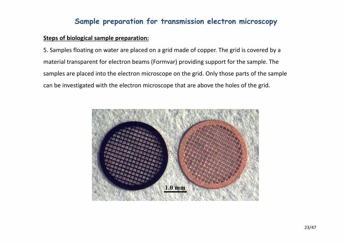
Steps of biological sample preparation:
5. Samples floating on water are placed on a grid made of copper. The grid is covered by a
material transparent for electron beams (Formvar) providing support for the sample. The
samples are placed into the electron microscope on the grid. Only those parts of the sample
can be investigated with the electron microscope that are above the holes of the grid.

24/47
Sample preparation for transmission electron microscopy
Steps of biological sample preparation:
6. Staining: it can be performed after putting the sample on the grid or just after fixation.
• Staining is required because biological samples provide very weak contrast (homogenous
thickness, homogenous distribution of atomic index).
• During staining the sample is treated with material containing atoms with high atomic
number.
• Types of staining:
o Positive staining: cell organelles are stained (e.g. lead acetate, uranyl acetate).
Osmium tetroxide stains the lipid component of membranes.
o Negative staining: leaves organelles preferentially unstained (e.g. phosphotungstic
acid).
25/47
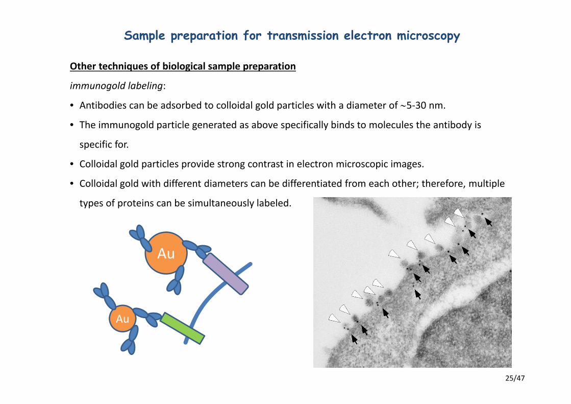
Sample preparation for transmission electron microscopy
Other techniques of biological sample preparation
immunogold labeling:
• Antibodies can be adsorbed to colloidal gold particles with a diameter of 5-30 nm.
• The immunogold particle generated as above specifically binds to molecules the antibody is
specific for.
• Colloidal gold particles provide strong contrast in electron microscopic images.
• Colloidal gold with different diameters can be differentiated from each other; therefore, multiple
types of proteins can be simultaneously labeled.
Au
Au

26/47
Sample preparation for electron microscopyOther techniques of biological sample preparation„metal tagging” (METTEM: metal-tagging TEM):
Au
25 nm
J Struct Biol 160:70-82.; Structure 20:759-766.; J Struct Biol 165:157-168.
15-20 nm
Problems of immunogold labeling:• only a fraction of proteins is labeled• the colloidal gold particle and the labeled
protein are relatively far from each other
A much higher number of gold particles can be seen with the METTEM technique.
+AuCl or AuCl3
unfolded MT tag(MT = metallothionein)
AuAu Au
AuAu
MT-gold nanocluster(1 nm)
The MT tag is fused to the gene of the protein of interest using molecular biological approaches; therefore, it is present in every copy of the given protein.
27/47
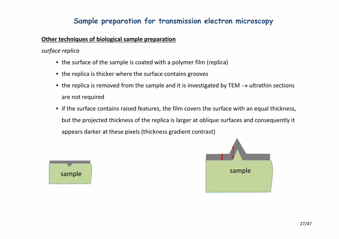
Sample preparation for transmission electron microscopy
Other techniques of biological sample preparation
surface replica
• the surface of the sample is coated with a polymer film (replica)
• the replica is thicker where the surface contains grooves
• the replica is removed from the sample and it is investigated by TEM ultrathin sections
are not required
• if the surface contains raised features, the film covers the surface with an equal thickness,
but the projected thickness of the replica is larger at oblique surfaces and consequently it
appears darker at these pixels (thickness gradient contrast)
sample sample

28/47
Sample preparation for transmission electron microscopy
Other techniques of biological sample preparation
shadowing:
• the surface replica provides relatively weak contrast (it is a carbon-containing polymer)
• platinum atoms are evaporated at an oblique angle on to the replica. Raised features
present in the replica cast sharp “shadows” within which platinum is absent.
replica
deposition of Pt
evaporation of Pt vapor
l
h
• the height of the raised feature can be estimated from the length of the shadow:
tanhl

29/47
Sample preparation for transmission electron microscopy
Methods for preparing ultrathin sections:
1. Ultramicrotome: for biological and other soft samples
2. Mechanical approach: a slice with a thickness of 1 mm is cut from which a disk with a
diameter of a couple of mm is cut (typically with an ultrasonic drill). The thickness of this disk is
further reduced, e.g. by grinding.
3. Chemical thinning: a chemical solution dissolves the original surface and reduces the specimen
thickness to a value suitable for TEM imaging.
4. Chemical jet thinning: material reacting with the surface is shot on to the surface.
5. Electrochemical thinning: the thickness of the sample is reduced due to electrolysis.
6. Ion beam thinning: 3mm-diameter thin disk of the material is placed in a vacuum system,
where it is bombarded by argon ions produced by a gas discharge within an ion gun. These ions
transfer energy to surface atoms and remove the material by the process of sputtering
7. Thin film deposition: the material is evaporated followed by its deposition on to a substrate
generating a thin film.

30/47
Scanning electron microscopy: interaction of the electron with the sample
increasing E0
increasing Z
penetration depth
electron beam
escape depth of
secondary electrons
secondary electrons generated at a large depth cannot leave the sample (they are absorbed within 1-2 nm)
backscattered electron: it can escape from the sample from a large depth due to its large energy
backscattered electron:• reflected from nuclei. Generated with a low
probability because the diameter of the nucleus is small
• its energy is approximately equal to that of primary electrons because it is generated by elastic scattering
secondary electron: • generated by ejection of
atomic electrons during inelastic scattering of primary electrons
• its energy is much lower than that of primary electrons
Escape depth: the distance from the surface at which secondary electrons
can still leave the sample. It is approximately 1-2 nm. Therefore, SEM examines the surface of the
sample.

31/47
Factors influencing the generation of secondary electrons
escape depth
At oblique surfaces the volume from which secondary electrons can escape is larger.
Edges stand out sharply in SEM images
3D effect
electron beam
escape depth
• Secondary electrons are mainly generated by
primary electrons which have already slowed down.
• Although more secondary electrons are generated at
high primary electron energies, most of the
secondary electrons are generated beyond the
escape depth.
• At large energies of primary electrons the number of
secondary electrons capable of leaving the material
decreases.
d
s
V d s
cosd sV
s
cosd

32/47
10 Å – Auger electrons
50-500 Å – secondary electrons, cathodoluminescence
characteristic X-ray
braking radiation
secondary fluorescence due to X-ray
Depths at which different signals are generated in SEM
current
backscattered electrons

33/47
Backscattered electrons
Backscattered electrons are usually generated as a result of elastic scattering; therefore, their energy is approximately equal to that of primary electrons
The energy of backscattered electrons is much larger than that of primary electrons.
The probability of generation of backscattered electrons increases with atomic number elements with high
atomic number are displayed more strongly.
Backscattered electrons can leave the sample from larger depths ( secondary
electrons can do so only from the surface).
Images generated by backscattered electrons show Z-contrast of thick surface
layers of the sample.
Simulated paths of primary electrons (blue)Backscattered electrons (red)20 keV
Backscattered electron image of Martian meteorite

34/47
Other detected signals in SEM
Specimen current Ip
IsecIBSE
Ispecimen
1 specimen p sec BSE pI I I I I
Ispecimen – current flowing across the specimenIp – primary-beam currentIsec – secondary-electron currentIBSE – backscattered-electron current – probability of generation of secondary electrons – probability of generation of backscattered electrons
Ispecimen is characteristic of specimen topography and specimen constitution (Z contrast).
Cathodoluminescence
Ener
gy
Valence band
Conduction band
hf
In certain semiconductors impinging electrons move an electron from the valance band to the conduction band. When the excited electron returns to the valence band, it emits fluorescence which is characteristic of the semiconductor.

35/47
Everhart-Thornley detector
Slow secondary electrons emitted into every direction of space are attracted to the detector by the positive voltage applied to the
Everhart-Thornley detector
Collection efficiency of secondary electrons• in the absence of positive
voltage: 5-10%• in the presence of positive
voltage: 90-100%
path of secondary electrons without positive voltage

36/47
Factors deteriorating resolution in SEM
secondary electrons (SE1)
backscattered electrons( )
secondary electrons generated by backscattered electrons (SE2)
metallic part of microscope
secondary electrons emitted from metallic parts of the microscope by backscattered electrons (SE3)
37/47
Sample preparation for SEM• It is typically much simpler than for TEM since ultrathin sections are not required.
• Problem: the specimen may undergo charging if the specimen current cannot flow to ground.
o If the specimen is conducting, charging is not a problem.
o If the specimen is not conducting (like most biological samples), its surface must be coated
with a thin film of conducting (metal) material.
o If coating with metal is not possible, specimen charging can often be avoided by carefully
choosing the SEM accelerating voltage so that the charge accumulating in the specimen is
approximately zero.
The equation describing specimen current: 1 specimen p sec BSE pI I I I I
If +=1, charge does not accumulate in the specimen!
1
E0
+
zero charging
region
The energy of primary electrons is low and they cannot generate secondary electrons. Consequently, +is small the electrons cannot leave the specimen; therefore it becomes negatively charged due to impinging primary electrons.
Secondary and backscattered electrons are generated deep in the specimen and they cannot escape electrons accumulate(negative charge).
If +<1, positive charging takes place, but it is not a problem since positive charge attracts secondary electrons back to the specimen and charge neutrality is restored.

38/47
Electron microscopy with biological samples: special conditions• Problems with biological samples:
o sensitive, fragileo important to retain physiological hydrated conditionso prevention of radiation damageo all of the above without sacrificing contrast
• Sample protection (from radiation, damaging effect of fixative):o negative staining: water surrounding the examined protein is replaced by heavy metal salt. In
this way the fixative does not damage the protein directly. The metal salt traces the contour of the protein.
o sealed thin window chamber: the specimen is isolated fromthe vacuum of the microscope with a thin berylliumfoil. In this way the specimen can remain hydrated.
o glucose embedding: the water content of the specimen is replaced by glucose. Water molecules bound tightly to proteins remain bound. Disadvantage: the contrast of glucoseresembles that of the protein, so it is difficult to differentiate proteins from glucose.
o environmental EM (discussed later)o cryo-EM (discussed later)
X-rayNMR
Cryoelectronmicroscope
Light microscope
10410 1012108 102410201016
(Daltons)

39/47
• Aim: the least possible damage of specimens during electron microscopy for structural biology byo avoiding the damage done by dehydration, fixation and stainingo reducing the radiation damage done by the electron beam
• Sample preparation: The hydrated sample is frozen suddenly by immersing it into liquid N2 (77 K = -196oC) or liquid ethane (189 K = -89 oC) in order to prevent the formation of ice crystals. The former applicable to protein samples only, while the latter can also be used for thin biological specimens (cells, viruses, etc.) since ethane
o does not form vapor on the surface of the specimen (↔liquid N2; therefore, the rate of cooling is slower for liquid N2)
o forms a thick condensed layer on the surface of the specimen (↔liquid N2; therefore, the rate of cooling is slower with liquid N2 due to the thin condensed layer formed)
• The instrument:
Cryo-electron microscopy 1
Styrofoam
Liquid Nitrogen Liq. EthaneGrid
Tweezer

40/47
• Imaging:o The specimen is images with low intensity radiation in order to minimize radiation damage
(→ due to the low number of electrons the quality of images is poor. This is improved by averaging many images).
Cryo-electron microscopy 2
Low resolution image Selection of particles
o The specimen is kept at low temperature (~110 K) in the vacuum of the EMo in order to prevent the sublimation of non-crystalline watero in order to immobilize molecule fragments and free radicals generated by the electron
beam and thereby avoid radiation damage.

41/47
o By investigating the specimen from different directions cryo-electron tomography can be performed.
Image classification
Cryo-electron microscopy 3

42/47
Environmental SEM
• Such a SEM in which the specimen does not need
to be placed in vacuum.
• p2<p1<p0, therefore the electron beam can collide
with gas molecules only at the end of its path it
is not scattered significantly.
• The specimen is not in vacuum; therefore
o it is not charged even without coating with
metal because negative charge accumulating
in the specimen is neutralized by positive ions
generated in the gas atmosphere by the
electron beam,
o the specimen does not need to be
dehydrated (under a pressure of 609 Pa fluid
water does not exist!!! Hydration is important
for the intactness of biological samples.)
43/47
Analytical electron microscopy
• Different signals induced by the electron beam contain information about the composition of the
specimen and the atomic indices of its constituent elements.
• Analytical electron microscopy is suitable for both qualitative and quantitative determination of
elements.
• Signals used for analytical electron microscopy:
o characteristic X-ray
o Auger electrons
o electron energy loss
o cathodoluminescence (not in the case of biological specimens)
44/47
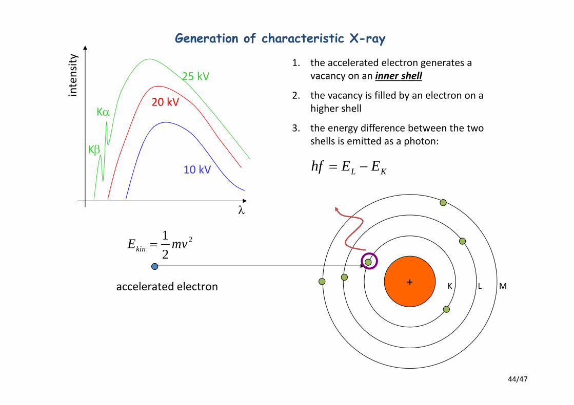
Generation of characteristic X-ray
10 kV
20 kV
inte
nsity
25 kV
K
K
+accelerated electron
2
21 mvEkin
1. the accelerated electron generates a vacancy on an inner shell
2. the vacancy is filled by an electron on a higher shell
3. the energy difference between the two shells is emitted as a photon:
KL EEhf
K L M

45/47
Generation of Auger electrons
+ K L M
vacancy generated by the accelerated electron
1. The vacancy generated by the accelerated electron is filled from a higher shell.
2. The energy released during the transition isn’t converted to a photon, but transferred to a nearby electron which leaves the atom.
Augerelectron

46/47
Analysis of characteristic X-ray
K, K, K
L, L
K
L
M
N
• The wavelength of characteristic X-ray is characteristic of the energy difference between inner electron shells, and its intensity is proportional to the quantity of the given element.
• There are two methods for the spectral analysis of X-ray:
Energy dispersive spectroscopy (XEDS –X-ray energy dispersive spectroscopy;
EDAX – energy dispersive analysis of X-ray)
Wavelength dispersive spectroscopy (XWDS –X-ray wavelength dispersive spectroscopy)
• X-ray photons are detected by a semiconductor diode
• the current impulse generated by the detector is proportional to the energy of the X-ray photon
ADVANTAGES:• approximately 1% of emitted X-ray photons
are detected, which is much more than in the case of XWDS fast
• relatively cheap
• X-ray photons are deflected to different directions according to their wavelength by a diffraction grating
• the detector always detects X-ray photons with only a certain wavelength
ADVANTAGES:• very good wavelength resolution
1
2
e- beam
specimen
X-ray
crystal
detector

47/47
Auger electron spectroscopy
Z
1
yiel
d
X-rayAuger electron
• In the case of elements with low atomic number the emission of characteristic X-ray has a low yield these elements cannot be investigated by X-ray spectroscopy.
• On the other hand, Auger electrons are generated with a much higher probability by elements with low atomic number.
• The energy of Auger electrons is characteristic of the given atom.
• Since the energy of Auger electrons is low (<1000 eV), they can be used for analyzing the surface layer of 1 nm thickness.
Electron energy loss spectroscopy (EELS)
• The energy loss of primary electrons going across the specimen is caused, among others, by the generation of vacancies in inner shells of atoms of the specimen ( characteristic X-ray, Auger electrons).
• Therefore, the energy loss of primary electrons is characteristic of the material of the specimen.• The energy of primary electrons is measured by magnetic spectrometers.• It can also be used for the analysis of elements with low atomic number.
30