Electron mean free path dependence of the vortex surface...
12
Electron mean free path dependence of the vortex surface impedance M Checchin 1,2 , M Martinello 1,2 , A Grassellino 1 , A Romanenko 1 and J F Zasadzinski 2 1 Fermi National Accelerator Laboratory, Batavia, IL 60510, USA 2 Department of Physics, Illinois Institute of Technology, Chicago, IL 60616, USA E-mail: [email protected] Received 14 September 2016, revised 2 December 2016 Accepted for publication 8 December 2016 Published 17 January 2017 Abstract In the present study the radio-frequency complex response of trapped vortices in superconductors is calculated and compared to experimental data previously published. The motion equation for a magnetic flux line is solved assuming a bi-dimensional and mean-free- path-dependent Lorentzian-shaped pinning potential. The resulting surface resistance shows the unprecedented bell-shaped trend as a function of the mean-free-path observed in our previous experimental work. We demonstrate that such bell-shaped trend of the surface resistance as a function of the mean-free-path may be described as the interplay of the two limiting regimes of the surface resistance, for low and large mean-free-path values: pinning and flux-flow regimes respectively. Since the possibility of defining the pinning potential at different locations from the surface and with different strengths, we discuss how the surface resistance is affected by different configurations of pinning sites. By tackling the frequency dependence of the surface resistance, we also demonstrate that the separation between pinning- and flux-flow-dominated regimes cannot be determined only by the depinning frequency. The dissipation regime can be tuned either by acting on the frequency or on the mean-free-path value. Keywords: RF superconductivity, vortex, vortex dynamics, vortex dissipation, mean free path dependence (Some figures may appear in colour only in the online journal) 1. Introduction When the superconductive transition is performed in the presence of an external magnetic field, magnetic flux can be trapped in the superconducting materials as energetically stable flux quanta in the mixed state of type-II super- conductors, or as magnetic flux pinned at defects in the Meissner state of type-I and type-II superconductors. In some circumstances, magnetic flux lines can penetrate in the Meissner state without the need of pinning sites and, as a consequence of the demagnetization effect, exist in the so- called intermediate state. Independently of their nature, any trapped magnetic flux structure can introduce dissipation in both dc and radio-frequency (rf) domains [1–4]. By controlling the pinning force of the superconducting material, it is possible to eliminate the vortex dc dissipation, enabling superconductors to transport very high currents, without any dissipation, up to the depinning current. By exceeding the depinning current, the dissipation due to vor- tices motion takes place because of the viscous drag force [5]. On the other hand, in rf applications the vortex dissipa- tion cannot be avoided most of the time. Even if pinned, the vortex flux line dissipates power because of the oscillation induced by the rf currents. Therefore, the trapped flux pro- blem is of critical importance for superconducting accelerat- ing cavities, especially when high quality factors are needed for their implementation in continuous wave accelerators. With the discovery of the nitrogen doping treatment [6], unprecedented high quality factors (Q-factors) are achievable Superconductor Science and Technology Supercond. Sci. Technol. 30 (2017) 034003 (12pp) doi:10.1088/1361-6668/aa5297 Original content from this work may be used under the terms of the Creative Commons Attribution 3.0 licence. Any further distribution of this work must maintain attribution to the author(s) and the title of the work, journal citation and DOI. 0953-2048/17/034003+12$33.00 © 2017 IOP Publishing Ltd Printed in the UK 1 FERMILAB-PUB-17-182-TD ACCEPTED Operated by Fermi Research Alliance, LLC under Contract No. DE-AC02-07CH11359 with the United States Department of Energy.
Transcript of Electron mean free path dependence of the vortex surface...
Electron mean free path dependence of thevortex surface impedance
M Checchin1,2, M Martinello1,2, A Grassellino1, A Romanenko1 andJ F Zasadzinski2
1 Fermi National Accelerator Laboratory, Batavia, IL 60510, USA2Department of Physics, Illinois Institute of Technology, Chicago, IL 60616, USA
E-mail: [email protected]
Received 14 September 2016, revised 2 December 2016Accepted for publication 8 December 2016Published 17 January 2017
AbstractIn the present study the radio-frequency complex response of trapped vortices insuperconductors is calculated and compared to experimental data previously published. Themotion equation for a magnetic flux line is solved assuming a bi-dimensional and mean-free-path-dependent Lorentzian-shaped pinning potential. The resulting surface resistance shows theunprecedented bell-shaped trend as a function of the mean-free-path observed in our previousexperimental work. We demonstrate that such bell-shaped trend of the surface resistance as afunction of the mean-free-path may be described as the interplay of the two limiting regimes ofthe surface resistance, for low and large mean-free-path values: pinning and flux-flow regimesrespectively. Since the possibility of defining the pinning potential at different locations from thesurface and with different strengths, we discuss how the surface resistance is affected bydifferent configurations of pinning sites. By tackling the frequency dependence of the surfaceresistance, we also demonstrate that the separation between pinning- and flux-flow-dominatedregimes cannot be determined only by the depinning frequency. The dissipation regime can betuned either by acting on the frequency or on the mean-free-path value.
Keywords: RF superconductivity, vortex, vortex dynamics, vortex dissipation, mean free pathdependence
(Some figures may appear in colour only in the online journal)
1. Introduction
When the superconductive transition is performed in thepresence of an external magnetic field, magnetic flux can betrapped in the superconducting materials as energeticallystable flux quanta in the mixed state of type-II super-conductors, or as magnetic flux pinned at defects in theMeissner state of type-I and type-II superconductors. In somecircumstances, magnetic flux lines can penetrate in theMeissner state without the need of pinning sites and, as aconsequence of the demagnetization effect, exist in the so-called intermediate state. Independently of their nature, any
trapped magnetic flux structure can introduce dissipation inboth dc and radio-frequency (rf) domains [1–4].
By controlling the pinning force of the superconductingmaterial, it is possible to eliminate the vortex dc dissipation,enabling superconductors to transport very high currents,without any dissipation, up to the depinning current. Byexceeding the depinning current, the dissipation due to vor-tices motion takes place because of the viscous drag force [5].
On the other hand, in rf applications the vortex dissipa-tion cannot be avoided most of the time. Even if pinned, thevortex flux line dissipates power because of the oscillationinduced by the rf currents. Therefore, the trapped flux pro-blem is of critical importance for superconducting accelerat-ing cavities, especially when high quality factors are neededfor their implementation in continuous wave accelerators.
With the discovery of the nitrogen doping treatment [6],unprecedented high quality factors (Q-factors) are achievable
Superconductor Science and Technology
Supercond. Sci. Technol. 30 (2017) 034003 (12pp) doi:10.1088/1361-6668/aa5297
Original content from this work may be used under the termsof the Creative Commons Attribution 3.0 licence. Any
further distribution of this work must maintain attribution to the author(s) andthe title of the work, journal citation and DOI.
0953-2048/17/034003+12$33.00 © 2017 IOP Publishing Ltd Printed in the UK1
FERMILAB-PUB-17-182-TD ACCEPTED
Operated by Fermi Research Alliance, LLC under Contract No. DE-AC02-07CH11359 with the United States Department of Energy.

in SRF niobium cavities. The presence of nitrogen as aninterstitial impurity in Nb allows for high Q-factors bydecreasing the temperature dependent part of the surfaceimpedance [7]. On the other hand, N-doped cavities showhigher dissipation per unit of magnetic flux trapped thanstandard cavities. It was indeed observed [8–10] that thevortex-related resistance per unit of trapped magnetic field is afunction of the electron mean-free-path, and therefore of thecavity thermal history. N-doped cavities operating at 1.3 GHzfall exactly in the mean-free-path region where the vortexdissipation is increased.
Two different approaches to describe the flux motionexist. The first one assumes a point-like description of a rigidvortex [11–15], where the pinning force is usually introducedas a restoring force independent of the distance of the pinningpoint from the rf surface.
The second approach assumes the flux line as a mono-dimensional object that possess a certain tension [3]. Usuallywhen this description is assumed the pinning force is dis-regarded [16, 17] and the vortex response is calculated inabsence of pinning.
If both vortex line tension and pinning force are con-sidered, the analytic form of the latter must possess thedependence on the distance from the rf surface, complicatingsubstantially the problem. A clever way to partially overcomethe problem is achieved by introducing Dirichlet boundaryconditions at the pinning site, as described in [18]. The maindrawback though is the impossibility of describing the pro-blem as a function of the pinning strength, which is one of themost important parameters to characterize the vortexdynamics in a superconductor as experimentally observed [4].
It is worth mentioning that, in case the vortex is gener-ated by the penetration of the rf field from the surface, and itis therefore parallel with respect to this latter, the defect-related pinning force can be disregarded [19], and theattractive force between the vortex and the surface [20] can beassumed as the unique restoring force.
In this paper, we propose a different approach. Themotion equation that describes the vortex displacement isdefined in such a way to be different for every point of theflux line, and hence dependent on the distance z from the rfsurface. To some extent, our approach is similar to the point-like description of the vortex response, but it differs from itsubstantially in terms of pinning force description. The ana-lytic form of the pinning potential adopted is dependent onthe distance z from the rf surface, therefore also the vortexline displacement is function of the distance from the rf sur-face. Differently than the point-like description where thevortex is extremely rigid and remains straight through theentire material thickness, our approach describes the motionof a flexible mono-dimensional vortex line.
The most noticeable point of our approach is its simpli-city and excellent description of the experimental dataacquired for SRF cavities [8–10]. The pinning force valuesused in order to interpolate the experimental data are in goodagreement with the pinning force of niobium found in lit-erature [21, 22]. The predicted values of depinning frequencyalso agree with those for niobium found in literature [23].
Introducing a clear dependence of the pinning force onthe electron mean-free-path l, the experimentally observedbell-shaped trend of the trapped flux surface resistance as afunction of the mean-free-path [8–10], can be explained as theinterplay of the resistivity calculated in flux-flow and pinningregimes.
In our preliminary study [24], we already demonstratedthat the trapped flux surface resistance is a function of themean-free-path and presents a maximum around 70 nm. Inany case, because of a too crude approximation assumed inthe calculation of the surface resistance and the adoption of amono-dimensional pinning potential, our previous approachsuggested that the dynamic contribution to the vortex dis-sipation generates largely overestimated values of surfaceresistance. Based on that, our past understanding was that thesurface resistance is of pure static origin, and therefore relatedonly to the normal-conducting nature of the vortex core. Bymeans of the more rigorous approach adopted in this study,we verify that the trapped flux surface impedance can bedescribed totally by the dynamic oscillation of vortices givenin [8–10].
Since vortices are usually multiple-pinned in the material,we take into account also situations where more than onepinning point per vortex is present. We will demonstrate that,in the case of SRF cavities, the position of the pinning point,their number and their strength are of extreme importance inorder to fully describe the experimental data.
We do also demonstrate that the transition between pin-ning and flux-flow regimes may be obtained not only bycrossing the depinning frequency [11], but also by tuning themean-free-path value of the superconducting material.
2. Single vortex resistivity
When trapped at the rf surface, the magnetic flux experiencesa force generated by the interaction with the Eddy currentsinduced by the oscillating rf field. The rf current density tj( )exercises a force on the magnetic flux quantum f0 in thevortex, accordingly to the Lorentz force. The magnetic forceacting on a single vortex per unit of length fL is:
^f f q= ´ = w l-f jj u sin e , 1Lt z
n0 0 0i∣ ∣ ( )
where j0 is the rf current, θ the angle between j and the normalto the rf surface un, ω the rf angular frequency andl l x= + l10 0( ) , with l0 the penetration depth (Londonpenetration depth), x0 the coherence length and l the elec-tronic mean-free-path.
We can write the motion equation of a single vortexsubjected to the Lorentz force as follows:
= + +M x t f f f¨ , 2L v p( ) ( )
with M being the inertial mass of the vortex per unit of lengthas defined by Bardeen and Stephen [25]:
p x
fa=M
nm B T2sin , 3
c2
04
2
0
2( )
( )
where Bc2 (= -B T T0 1c c22( )[ ( ) ]) is the upper critical field,
2
Supercond. Sci. Technol. 30 (2017) 034003 M Checchin et al

α the Hall angle with respect the normal to j defined in [25]as:
af tp x
=e
mtan , 40
02
( )
e and m are the charge and mass of the electron, respectively,and t = l vf the electron relaxation time, with vf the Fermivelocity.
The other forces acting on the vortex are fp the pinningforce and fv the viscous drag force. In our description we areneglecting instead the Magnus force and the interactionbetween vortices, since we assume H Hc2.
The viscous drag force is defined as h= -f xv ˙ where η isthe vortex drag coefficient per unit of length.
Bardeen and Stephen [25] describes the resistance relatedto the viscous drag force as generated by the Joule dissipationdue to the normal-conductive currents induced in the vortexcore while the flux is moving.
The different approach adopted by Tinkham [26] is basedon the relaxation time of the order parameter for a movingvortex. The order parameter of a vortex in a superconductorvaries from its equilibrium value to zero at the vortex center[27], moving from its previous to its next position, the vortexleaves a non-equilibrium-order-parameter trace behind it,since a finite relaxation period passes before the order para-meter returns to its equilibrium value. Because of the exis-tence of such finite relaxation time some condensation energyis lost, as if a force was acting against the flux motion—theviscous drag force.
Both the approaches gives comparable results of η in theT Tc limit (with Tc the critical temperature). While, in
approximation T Tc, Gor’kov and Kopnin [16] calculated η
connecting its changing rate to the variation in condensationenergy, in the framework of the Ginzburg-Landau theory.
For the purpose of our work, we will adopt the Bardeenand Stephen [25] definition, since our area of interest is in thelimit T Tc. The viscous drag coefficient per unit of lengthis then defined as:
hf
r=l T
B T, , 5c
n
0 2( )( )
( )
where rn ( t= -ne m2 1( ) ) is the normal conducting resistivity.
The pinning force description is extremely complicatedand related to the nature of the pinning sites [2, 28]. In thepresent study, we do not discriminate between different typesof pinning centers, thus we assume an idealistic description ofthe pinning potential.
The ideal mono-dimensional pinning potential is afunction of the effective coherence length ξ( x= + -l1 10
1( ) ) and is described by an inverse Lorentzianfunction [29] (as shown in figures 1(b)). Since the vortex is alinear object, the pinning site will be localized at a certaindistance q from the rf surface. The associated pinningpotential has centroid at such pinning position and approacheszero in every direction far from it.
By adopting a bi-dimensional Lorentzian potential andby limiting the pinning interaction along the oscillation
direction (x), we are able to simplify the problemsignificantly.
In order to solve analytically the motion equation of thevortex, we transform it to a linear equation in x by expandingthe pinning potential to the second order with respect to x (asshown in figure 1(b)).
å
å å
xx
xx
xx
= -+ + -
» -+ -
++ -
=
= =
U x z lU
x z q
U
z q
U
z qx
, ,
,
6
pi
n
i
i
n
i i
n
i
0
02
2 2 2
0
02
2 20
02
2 2 22
i
i i
( )( )
( ) [ ( ) ]( )
where U0iis the potential depth per unit of length of the ith
pinning point, while the sum accounts for multiple pinningpotentials centered at the qith positions acting on the samevortex.
Figure 1. (a) Tri-dimensional representation of the pinning potentialconsidered, (b) contour plot of two pinning potential acting on thefame flux line. The two graphs defined as 1 and 2 are respectively thecross section of the pinning potential along x and along z.
3
Supercond. Sci. Technol. 30 (2017) 034003 M Checchin et al
A single pinning potential is then parabolic along thedirection of oscillation and Lorentzian along z. The tri-dimensional representation of the pinning potential con-sidered is plotted in figure 1(a), while in figure 1(b) anexample of an oscillating flux line subjected to two potentialsin series is shown. Figure 1(b) shows also the sections of thepinning potential along x and z, and the positions of the twopinning points (q1 and q2).
The pinning force per unit of length is then defined as:
åx
x
=-¶¶
=-+ -
=-=
f x z lx
U
U
z qx
p z l x
, ,
2
, , 7
p p
i
n
i0
02
2 2 2i
( )
( ( ) )( ) ( )
with pinning constant p z l,( ).Substituting equations (1), (7) and the viscous drag force
with η equal to equation (5) in equation (2), we get the motionequation of a single vortex:
a b g+ + = wx z t l x z t l x z t l¨ , , , , , , e , 8t2 i( ) ˙ ( ) ( ) ( )
which corresponds to a driven-dumped oscillator secondorder differential equation, with a h= M , b = p M2 ,g f q= j Msin0 and = l-j j e z
0 .The solution of such a differential equation is:
= + wx z t l A A, , i e , 9t1 2
i( ) ( ) ( )
where:
f q ww hwf q hww hw
=-
- +
=-- +
A z lj p M
p M
A z lj
p M
,sin
,
,sin
. 10
10
2
2 2 2
20
2 2 2
( )( )
( ) ( )
( )( ) ( )
( )
We can now calculate the average (active) dissipatedpower á ñP and the reactive power á ñQ per unit of volume as:
⎜ ⎟⎧⎨⎩
⎛⎝
⎞⎠
⎫⎬⎭
ò
ò
á ñ=
á ñ= -
P z lT
F t x z t l t
Q z lT
F t x z tT
l t
,1
Re , , d ,
,1
Im ,4
, d , 11
T
L
T
L
0
0
( ) { ( ) ( )}
( ) ( ) ( )
where T is the rf period ( p w=T 2 ), q=F jB sinL v is theLorentz force per unit of volume, with Bv the vortex magn-etic field.
Solving the two integrals for the real and imaginary partsof Lorentz force and vortex velocity x z t l, ,˙ ( ), we obtain theapparent power per unit of volume:
wf qw hw
hw w
r
á ñ = á ñ + á ñ
=- +
+ -
=
S z l P Q
B
p Mp M j
j
, i
sin
2i
1
2,
12
v02
2 2 22 2
2
( )
[( ) ( ) ][ ( )]
( )
where ρ is the complex vortex resistivity.
Since f px=Bv 0 02, where px0
2 is the vortex core area,the complex vortex resistivity ρ is then equal to:
r r r
wf q
px w hwhw w
= +
=- +
+ -
z l
p Mp M
, i
sini ,
13
1 2
02 2
02 2 2 2
2
( )
[( ) ( ) ][ ( )]
( )
where r1 and r2 respectively describe the resistive and reac-tive behavior of the vortex when subjected to a rf current.
2.1. Flux-flow regime
In the large mean-free-path limit, the vortex dissipation isdescribed by the flux-flow regime. In such a limit, we canneglect the pinning force ( ~p 0) since the pinning potentialbecomes very shallow driven by the longer coherence length.
On the other hand, the viscous coefficient (equation (5))is larger because of its dependence on the normal-stateresistivity (the longer l, the smaller rn and the larger η).Therefore, the main force acting on the vortex is the viscousdrag force. Since very small compared to η, the vortexʼsinertial mass can be neglected as well.
Neglecting inertial and pinning terms, we can rewrite themotion equation (equation (8)) as:
a g= wx z t l, , e . 14ti˙ ( ) ( )
This first order differential equation can be easily solvedby meaning of the ansatz used above (equation (9)). Solvingthe equation, we obtain an imaginary coefficient:
f qwh
= -A lj sin
, 1520( ) ( )
and calculating the apparent power in equation (12), we get apurely real resistivity:
rf q
px h=l
sin. 161
02 2
02
( ) ( )
Such a definition of the flux-flow resistivity is equivalentto the result obtained by Kim et al [5] and by Marcon et al[13] (real part). We should also notice that the same form ofr1 can be obtained by neglecting the term w-p M 2 2( ) inequation (13).
This result suggests that the vortex dissipation for largemean-free-path values is independent on the frequency anddepends only on the mean-free-path.
Moreover, as the purity of the material increases (lincreases) the resistivity decreases since it is inversely pro-portional to the viscous coefficient η. For big enough mean-free-path values, the resistivity is minimized, and the dis-sipation introduced by the vortex oscillation negligible.
2.2. Pinning regime
In the limit of small mean-free-path values, we can define thepinning regime. Since η decreases with decreasing l, theviscous drag force is negligible in the small l limit. On thecontrary, the pinning force is larger due to a shorter coherencelength which increases the steepness of the pinning potential.
4
Supercond. Sci. Technol. 30 (2017) 034003 M Checchin et al
In this regime, the main force acting on the vortex is thepinning force, and the vortex inertial mass may also beneglected.
Considering the complex resisitivity defined inequation (13), we can obtain a form of ρ that describes thevortex impedance in the pinning regime for intermediate valuesof mean-free-path. As already discussed, for small l values thedominant contribution is the pinning force. Therefore,neglecting the inertial term wM 2 and rewriting the denominatoras px p0
2 2, we can define the complex resistivity as:
rwf q
pxhw= +z l
pp,
sini . 170
2 2
02 2
( ) [ ] ( )
In such an intermediate regime, the vortex response is bothof resisitive and reactive nature. The decreasing of the p2 with lis more rapid than the increasing of η, thus r1 increases with l.Also, in the pinning regime r1 is proportional to w2.
On the opposite, as the mean-free-path decreases, the realpart decreases with it until it becomes negligible. Such alimiting condition is well described by the vortex motionequation where both the inertial and viscous contributions areneglected:
b g= wx z t l, , e . 18t2 i( ) ( )
Solving for x and comparing with the ansatz inequation (9), we obtain a pure real coefficient:
f q=A z l
j
p,
sin, 191
0( ) ( )
and the apparent power in equation (12) is totally reactive.Thus, the reactive response of the vortex oscillation is purelyreactive:
rwf q
px=z l
p,
sin. 202
02 2
02
( ) ( )
Such a result suggests that for low mean-free-paths, avortex interacting with the oscillating field does not contributeto active power dissipation, its response is purely reactive.Moreover, in the limit of very small mean-free-paths, thepinning constant (p) increases substantially and minimizes thereactive response as well.
3. Vortices surface impedance
Now that the vortex resistivity is known, the surface impe-dance for a single vortex is calculated assuming the classicdefinition:
⎡⎣⎢
⎤⎦⎥
ò
ò r
=
=l
¥
¥ - -
Z lE
j z z
z lz
0
d
e
,d , 21
x
x
z
1
0
0
1
( ) ( )
( )
( )( )
where = l-j z j exz
0( ) .In the non-local description, a quantized flux line is
represented as a modulation of the order parameter of the
superconductor that tends to zero at the center of the vortex,and approaches to its finite value far from it [27].
Differently, in the local description [33], the vortex isdescribed as a normal conducting core with dimension of theorder of the coherence length x0, with superconducting cur-rents spinning around it and screening the magnetic fluxconfined inside. In this scenario, when a finite value ofmagnetic field (B) is applied to the superconductor during thetransition, N vortices are created, and each of them carries amagnetic flux quantum f0 through an area px0
2, i.e.f =N AB0 , where A is the normal conducting area that
experiences the magnetic field at transition.We can therefore extend the single vortex resistance
defined in equation (21) to a multi-vortex resistance multi-plying by the fraction of the area occupied by the trappedvortices px px f=N A B0
202
0.Now, we should consider that most likely there will be a
certain distribution of pinning potentials in the material. Inorder to take into account that, we define the probabilitydensity of finding the pinning point at the position qi as G qi( ),and the probability density that a pinning potential hasstrength U0i
as L U0i( ).The real forms of G qi( ) and L U0i( ) are unknown, there-
fore both of them will be described by a normalized Gaussiandistribution. The G qi( ) probability density has variance sqi
andcentroid qi
0:
⎜ ⎟ ⎜ ⎟⎛⎝
⎞⎠
⎛⎝
⎞⎠
G =
=+
s
ps
s s
--
-
q B
B
e ,
Erf Erf, 22
i i
q q
iq q q
2
2
2 2
i i
qi
qi
i i
qi
i
qi
02
2
2
0 0
( )
( )
( )
with qi the maximum extension of the integration domainover all the possible positions qi, defined as s+q 5 q0i i
. Whilethe probability density L U0i( ) has variance sU i0 and centroid
U00i:
⎜ ⎟ ⎜ ⎟⎛⎝
⎞⎠
⎛⎝
⎞⎠
L =
=-
s
ps
s s
--
- -
U C
C
e ,
Erf Erf, 23
i
U U
iU U U U
02
2
2 2
i
i i
U i
U i
i i
U i
i i
U i
0 00 2
02
02
0 00
0
0 00
0
( )
( )
( )
where U0iand U0i
are the extremes of the integration domain,
set as sU 5 U00i i0 . If s- <U 5 0U0
0i i0 , then =U 00i
, since nonegative pinning strength values are allowed.
The vortices surface impedance weighted over pinningpoint position and strength distributions, for a given trappedfield B is defined as:
ò ò ò ò
ò
px
f=
G L
r
=l
-
Z lB
q U
zU q U q
dd d d d , 24
q
U
U q
U
U
i
ni
L
z
n
02
0 0 0
0 0
0
e0 0 0
o
n
n
n
i
zn
0
0
00
0
0
0
( )
[ ( ) ( )]( )
( )
5
Supercond. Sci. Technol. 30 (2017) 034003 M Checchin et al

with L being the cavity wall thickness.
In order to simplify the interpretation of the simulationresults, we adopt a Dirac-δ distribution for both G qi( ) andL U0i( )—instead of the more realistic Gaussian probabilitydensity function—and a single pinning point with
=q 20 nm0 and º =U U 1.1 MeV00
00m–1, in all the simu-
lation performed (if not differently specified). All the otherparameters used are reported in table 1.
In figure 2, we plot the real part of the vortices surfaceimpedance normalized to the trapped magnetic field B as afunction of the electron mean-free-path l, calculated from thereal part of the resistivity defined in equation (13). In the sameplot we show also the two limits for clean and dirty materials(flux-flow and pinning regimes), calculated withequations (16) and (17), respectively.
In the inset of figure 2, the imaginary part of the surfaceimpedance is reported. Its behavior is roughly opposite to thereal part, but with absolute value about two orders of mag-nitude lower than the latter, and therefore negligible.
The most noticeable feature shown in figure 2 is thepresence of a peak in the surface resistance around 70 nm. Forlarge mean-free-paths, the surface resistance follows perfectlythe flux-flow result and decreases with the cleanliness of thematerial.
On the opposite, when the the mean-free-path decreases,the surface resistance deviates substantially from the flux-flowregime, approaching to the pinning regime.
Starting in the large mean-free-path region (flux-flowregime) and moving towards small mean-free-path values(pinning regime) both the pinning constant p and the viscousdrag coefficient η are subjected to a substantial variation. Inparticular, p increases driven by the decreased coherence
length, while η decreases because of the lower normal-stateconductivity.
The decreasing of the surface resisitance in the pinningregime can be explained by the vanishing of the real part ofthe resistivity for small mean-free-path values, as discussed insection 2.2. For very dirty materials, the drag coefficient canbe neglected, and the vortices response to a rf field is purelyreactive.
For large mean-free-paths instead, the situation is theopposite. As discussed in section 2.1, for very large values ofmean-free-path the resistivity is purely real, but the dragcoefficient is so large that the vortices response is weak andthe surface impedance tends to zero—less movable vorticesdissipate less.
The peak is then generated by the interplay of flux-flowand flux pinning regimes. In other words, we observe theprogressing variation of the vortices response from purelyreactive—low mean-free-paths, to purely resisitive—largemean-free-paths.
3.1. Pinning strength dependence
The pinning strength U0 is a parameter that modifies thepinning constant p, and therefore the pinning force(equation (7)). In order to visualize the effect of different U0
on the surface resistance, we plot in figure 3, the real part ofthe surface impedance as a function of the mean-free-path forincreasing values of pinning strength U0. As shown, thesurface resistance peak is decreased in height and its positionshifted to larger mean-free-path values for increasing valuesof U0.
Since p increases linearly with U0, we expect that thepinning force is becoming larger and larger for increasing U0.Such a variation affects the maximum of the surface resist-ance and shifts it towards larger mean-free-path values.
A larger pinning force implies a wider mean-free-pathrange within which the pinning regime is favorable than theflux-flow regime. In such a scenario, larger values of l areneeded to decrease the pinning force and make it negligiblewith respect to the the viscous drag force. This differentbalance of the forces in play results in a higher mean-free-path onset for the flux-flow regime, and the surface resistancepeak is shifted to larger values.
Figure 2. Real part of the surface impedance as a function of themean-free-path. The dashed-dotted lines correspond to the pinningand flux-flow regimes, for small and large mean-free-path values,respectively. In the inset the imaginary part of surface impedance isplotted as a function of the mean-free-path.
Table 1. Parameters values used in the simulations for niobium.
Parameter Value Reference
x0 ´ -38 10 9 m [30]l0 ´ -39 10 9 m [30]B 0c2 ( ) 442 mT [31]vf ´1.37 106 m s−1 [32]n ´5.56 1028 m−3 [32]f ´1.3 109 HzT 1.5 KL 3 mm
6
Supercond. Sci. Technol. 30 (2017) 034003 M Checchin et al

3.2. Multiple pinning
We now analyze the situation in which multiple pinningpoints are present per single flux line. From now on weshould consider that the vortex oscillation is extended beyondthe rf layer, where the rf currents are present. An example ofvortex oscillation is reported in figure 4(a), where the vortexdisplacement normalized to the current density amplitude atthe surface j0 is plotted as a function of the depth z for suc-cessive time instants (with p w=T 2 the rf period).
In the simulation of figure 4(a), two pinning points withsame strength =U 1.1 MeV0 m–1 are assumed at 80nm and200nm respectively. As shown, the vortex displacement isnot rigid. Depending on the local pinning force and currentdensity level, it has different oscillation amplitudes. Thevortex displacement is minimum at the pinning sites, while itincreases far from them. It is worth mentioning also that, atthe same temporal instant, different sections of the vortex mayassume displacements of opposite sign, because of the vortexcomplex response.
As a result of such flexible vortex oscillation, the powerabsorption is dependent on the whole fraction of an oscillatingvortex. The active power is indeed dependent on the distancefrom the rf layer as shown by the z dependence ofequation (12). In figure 4(b), the active power per unit ofvolume normalized with respect to j0
2 (for the vortex dis-placement shown in figure 4(a)) is reported. In correspon-dence of the pinning points (arrows), the dissipation isdecreased of about four orders of magnitude because of thestronger local restoring force. Far from the pinning points, thevortex line has more freedom and the dissipation is indeedlarger.
The surface resistance dependence on the distance andnumber of pinning points from the rf surface is reported infigure 5(a). The real part of the vortices surface impedance(equation (24)) was calculated considering again a Dirac-δdistribution profile, but considering one, two or three pinningpoints.
Curve a considers only one pinning point in the wholevortex line. The surface resistance is approximately constantfor a pinning point positioned 1–2nm from the rf surface, ithas a minimum for q0 around 15nm and it returns constantfor >q 200 nm0 . The effect of a pinning point is equivalentto a constraint on the flux line oscillation in the material. If thepinning point is too far from the rf surface ( lq0 ), then thedissipation will reach its constant and maximum value sincethe oscillation is wider. Indeed, when the pinning point is farenough from the rf surface, the vortex oscillation is not per-turbed by the presence of the pinning point, and the effect isequivalent to the condition when no pinning points are pre-sent at all.
If the pinning point is near the surface, the vortexoscillation amplitude is large on both sides of the pinningpoint (as shown in figure 4(a)) and the position of the pinningpoint will define the magnitude of the dissipation. Infigure 5(a), the minimum of the surface resistance falls atabout 15nm, which is roughly comparable to half of thepenetration dept for niobium with l=70nm (l ~ 48 nm). Insuch condition the vortex is well constrained and the resist-ance minimized, since both the two sides of the flux line(above and below the pinning point) have restrained oscilla-tion amplitudes.
Let us examine curve b in figure 5(a). For such curve thecoordinate q0 corresponds to the position of the second pin-ning point, while the first one was assumed fixed at
=q 2 nm01from the surface (red dot on the curve). The first
noticeable effect is the overall lowering of the surfaceresistance for all the values of q0. When q0 increases above10nm the surface resistance increases and approaches itsconstant value for >q 200 nm0 .
Interesting to notice that the surface resistance plateau for>q 200 nm0 of curve b corresponds to the surface resistance
value obtained for a single pinning point at 2nm (green uptriangle— —on curve a). This means that if q0 is too largethe second pinning point does not perturb the vortex behavior.
Adding a second fixed pinning point at =q 20 nm02(red
dots) and defining the abscissa as the position of the thirdpinning point, we obtain curve c (figure 5(a)). Also this timethe surface resistance value is lowered for all the q0 values. Asin the double pinning case, the surface resistance is constantabove a certain threshold ( >q 1000 nm), and approaches thevalues it would have if only two pinning points were present(green diamond— —on curve b).
In figure 5(b), the surface resistance as a function of themean-free-path is instead shown. The simulation was per-formed considering one (curve 1), two (curve 2) and three(curve 3) pinning points per vortex line, positioned at 2nm, 2and 20nm and 2, 20 and 50nm respectively.
Since the pinning point number and position play a roleonly in the low mean-free-path region, as expected, no var-iation of the mean-free-path dependence are shown in theflux-flow regime range. Noticeable variations of the trend areinstead observable in the peak position and in the low mean-free-path region.
In case of multiple pinning, the peak changes positionand moves towards larger mean-free-path values. Such a
Figure 3. Real part of the surface impedance as a function of themean-free-path for different values of U0.
7
Supercond. Sci. Technol. 30 (2017) 034003 M Checchin et al

phenomenon is a symptom of an overall larger pinning force,i.e. the flux-flow regime starts to take over at larger values ofmean-free-path. Such a larger pinning force acts also on thepeak height, which is lowered in case of multiple pinning.Therefore a larger number of pinning points assures lowerresistance. The green points with same shape in figures 5(a)and (b) (up triangle— , diamond— and down triangle— )refers to surface resistance values calculated with the sameparameters as reported in table 2.
3.3. Frequency dependence
Up to this point we have considered always 1.3GHz as aconstant frequency. Such a frequency was selected inasmuchas it is the most commonly used in SRF basic research and
lots of experimental data are available. On the other handthough, the frequency dependence of the vortex surfaceimpedance is of extreme importance.
Figure 6(a) shows the dependence of the real part of thevortices surface impedance as a function of the exciting
Figure 4. In (a) simulation of the vortex displacement normalized to j0 as a function of the depth for different time instants in units of rf periodT. In (b) the average power per unit of volume normalized to j0
2 in instead reported. Both the simulations were performed assumingl=10nm, =U 1.1 MeV0 and two pinning points at 80 and 200nm.
Figure 5. In (a) simulations of the surface resistance as a function of the pinning point position are reported. For all three the curvesl=70 nm and =U 1.1 MeV0 m–1. Curve a considers only one variable pinning point position, curve b one fixed and one variable pinningpoint positions and curve c two fixed and one variable pinning point positions. In (b) the surface impedance as a function of the mean-free-path is reported in the condition of single (1), double (2) and triple (3) pinning per vortex flux line. The pinning points positions are reportedin table 2.
Table 2. Pinning point positions of the green points in figure 5. Forall the points =U 250 meV and l=70 nm.
Point Pinning points position
=q 201nm
=q 2 nm01, =q 2002
nm
=q 2 nm01, =q 20 nm02
, =q 5003nm
8
Supercond. Sci. Technol. 30 (2017) 034003 M Checchin et al
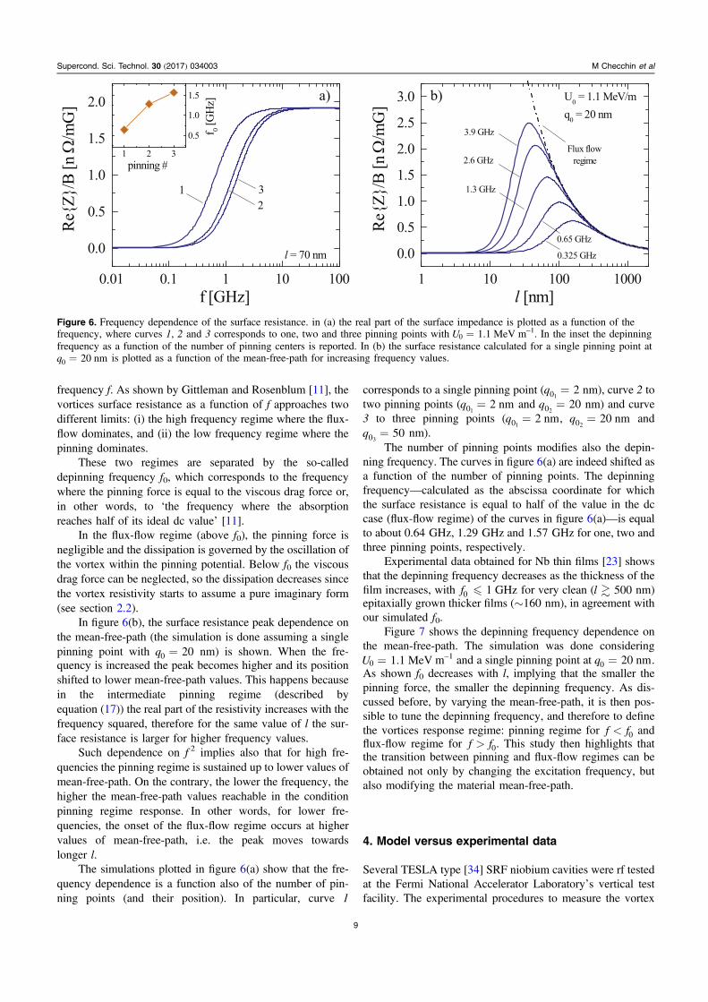
frequency f. As shown by Gittleman and Rosenblum [11], thevortices surface resistance as a function of f approaches twodifferent limits: (i) the high frequency regime where the flux-flow dominates, and (ii) the low frequency regime where thepinning dominates.
These two regimes are separated by the so-calleddepinning frequency f0, which corresponds to the frequencywhere the pinning force is equal to the viscous drag force or,in other words, to ‘the frequency where the absorptionreaches half of its ideal dc value’ [11].
In the flux-flow regime (above f0), the pinning force isnegligible and the dissipation is governed by the oscillation ofthe vortex within the pinning potential. Below f0 the viscousdrag force can be neglected, so the dissipation decreases sincethe vortex resistivity starts to assume a pure imaginary form(see section 2.2).
In figure 6(b), the surface resistance peak dependence onthe mean-free-path (the simulation is done assuming a singlepinning point with =q 200 nm) is shown. When the fre-quency is increased the peak becomes higher and its positionshifted to lower mean-free-path values. This happens becausein the intermediate pinning regime (described byequation (17)) the real part of the resistivity increases with thefrequency squared, therefore for the same value of l the sur-face resistance is larger for higher frequency values.
Such dependence on f 2 implies also that for high fre-quencies the pinning regime is sustained up to lower values ofmean-free-path. On the contrary, the lower the frequency, thehigher the mean-free-path values reachable in the conditionpinning regime response. In other words, for lower fre-quencies, the onset of the flux-flow regime occurs at highervalues of mean-free-path, i.e. the peak moves towardslonger l.
The simulations plotted in figure 6(a) show that the fre-quency dependence is a function also of the number of pin-ning points (and their position). In particular, curve 1
corresponds to a single pinning point ( =q 201nm), curve 2 to
two pinning points ( =q 2 nm01and =q 2002
nm) and curve3 to three pinning points ( =q 2 nm01
, =q 20 nm02and
=q 5003nm).
The number of pinning points modifies also the depin-ning frequency. The curves in figure 6(a) are indeed shifted asa function of the number of pinning points. The depinningfrequency—calculated as the abscissa coordinate for whichthe surface resistance is equal to half of the value in the dccase (flux-flow regime) of the curves in figure 6(a)—is equalto about 0.64GHz, 1.29GHz and 1.57GHz for one, two andthree pinning points, respectively.
Experimental data obtained for Nb thin films [23] showsthat the depinning frequency decreases as the thickness of thefilm increases, with f 1 GHz0 for very clean ( l 500 nm)epitaxially grown thicker films (∼160nm), in agreement withour simulated f0.
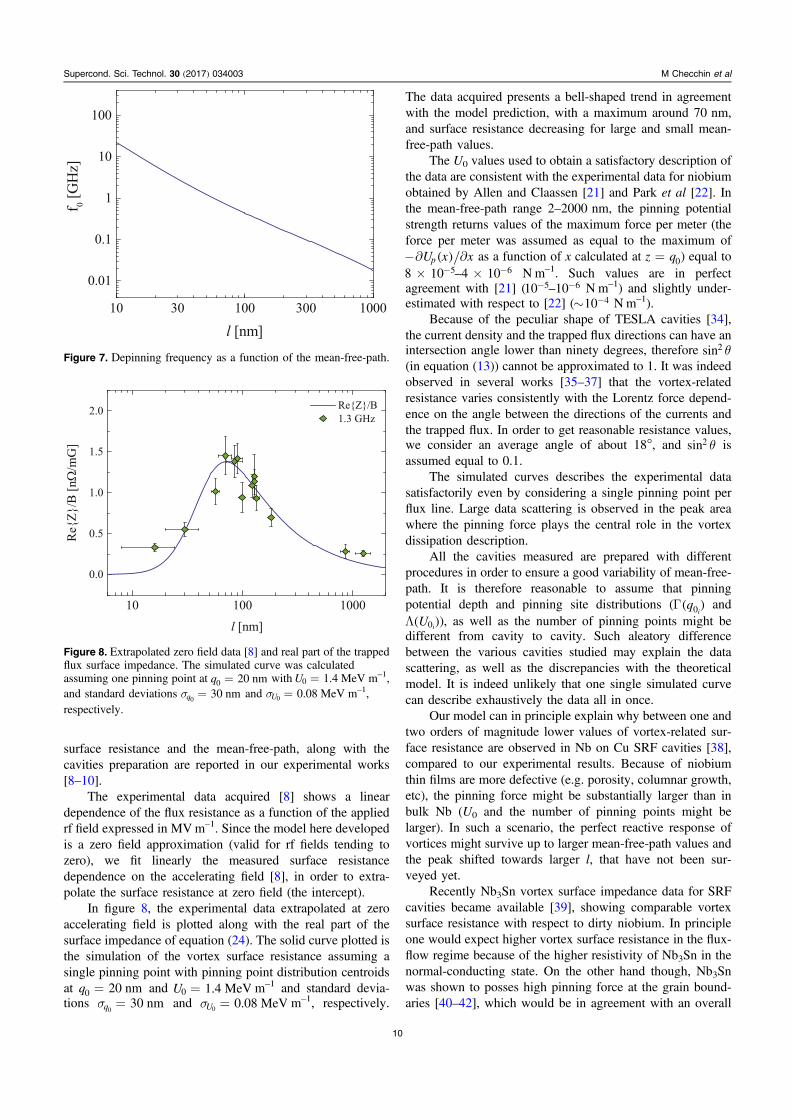
Figure 7 shows the depinning frequency dependence onthe mean-free-path. The simulation was done considering
=U 1.1 MeV0 m–1 and a single pinning point at =q 20 nm0 .As shown f0 decreases with l, implying that the smaller thepinning force, the smaller the depinning frequency. As dis-cussed before, by varying the mean-free-path, it is then pos-sible to tune the depinning frequency, and therefore to definethe vortices response regime: pinning regime for <f f0 andflux-flow regime for >f f0. This study then highlights thatthe transition between pinning and flux-flow regimes can beobtained not only by changing the excitation frequency, butalso modifying the material mean-free-path.
4. Model versus experimental data
Several TESLA type [34] SRF niobium cavities were rf testedat the Fermi National Accelerator Laboratoryʼs vertical testfacility. The experimental procedures to measure the vortex
Figure 6. Frequency dependence of the surface resistance. in (a) the real part of the surface impedance is plotted as a function of thefrequency, where curves 1, 2 and 3 corresponds to one, two and three pinning points with =U 1.1 MeV0 m–1. In the inset the depinningfrequency as a function of the number of pinning centers is reported. In (b) the surface resistance calculated for a single pinning point at
=q 20 nm0 is plotted as a function of the mean-free-path for increasing frequency values.
9
Supercond. Sci. Technol. 30 (2017) 034003 M Checchin et al
surface resistance and the mean-free-path, along with thecavities preparation are reported in our experimental works[8–10].
The experimental data acquired [8] shows a lineardependence of the flux resistance as a function of the appliedrf field expressed in MVm–1. Since the model here developedis a zero field approximation (valid for rf fields tending tozero), we fit linearly the measured surface resistancedependence on the accelerating field [8], in order to extra-polate the surface resistance at zero field (the intercept).
In figure 8, the experimental data extrapolated at zeroaccelerating field is plotted along with the real part of thesurface impedance of equation (24). The solid curve plotted isthe simulation of the vortex surface resistance assuming asingle pinning point with pinning point distribution centroidsat =q 20 nm0 and =U 1.4 MeV0 m–1 and standard devia-tions s = 30 nmq0
and s = 0.08 MeVU0m–1, respectively.
The data acquired presents a bell-shaped trend in agreementwith the model prediction, with a maximum around 70nm,and surface resistance decreasing for large and small mean-free-path values.
The U0 values used to obtain a satisfactory description ofthe data are consistent with the experimental data for niobiumobtained by Allen and Claassen [21] and Park et al [22]. Inthe mean-free-path range 2–2000nm, the pinning potentialstrength returns values of the maximum force per meter (theforce per meter was assumed as equal to the maximum of-¶ ¶U x xp ( ) as a function of x calculated at =z q0) equal to´ ´- -8 10 4 105 6– Nm–1. Such values are in perfect
agreement with [21] ( - -10 105 6– Nm–1) and slightly under-estimated with respect to [22] (~ -10 4 Nm–1).
Because of the peculiar shape of TESLA cavities [34],the current density and the trapped flux directions can have anintersection angle lower than ninety degrees, therefore qsin2
(in equation (13)) cannot be approximated to 1. It was indeedobserved in several works [35–37] that the vortex-relatedresistance varies consistently with the Lorentz force depend-ence on the angle between the directions of the currents andthe trapped flux. In order to get reasonable resistance values,we consider an average angle of about 18°, and qsin2 isassumed equal to 0.1.
The simulated curves describes the experimental datasatisfactorily even by considering a single pinning point perflux line. Large data scattering is observed in the peak areawhere the pinning force plays the central role in the vortexdissipation description.
All the cavities measured are prepared with differentprocedures in order to ensure a good variability of mean-free-path. It is therefore reasonable to assume that pinningpotential depth and pinning site distributions (G q0i
( ) andL U0i( )), as well as the number of pinning points might bedifferent from cavity to cavity. Such aleatory differencebetween the various cavities studied may explain the datascattering, as well as the discrepancies with the theoreticalmodel. It is indeed unlikely that one single simulated curvecan describe exhaustively the data all in once.
Our model can in principle explain why between one andtwo orders of magnitude lower values of vortex-related sur-face resistance are observed in Nb on Cu SRF cavities [38],compared to our experimental results. Because of niobiumthin films are more defective (e.g. porosity, columnar growth,etc), the pinning force might be substantially larger than inbulk Nb (U0 and the number of pinning points might belarger). In such a scenario, the perfect reactive response ofvortices might survive up to larger mean-free-path values andthe peak shifted towards larger l, that have not been sur-veyed yet.
Recently Nb3Sn vortex surface impedance data for SRFcavities became available [39], showing comparable vortexsurface resistance with respect to dirty niobium. In principleone would expect higher vortex surface resistance in the flux-flow regime because of the higher resistivity of Nb3Sn in thenormal-conducting state. On the other hand though, Nb3Snwas shown to posses high pinning force at the grain bound-aries [40–42], which would be in agreement with an overall
Figure 7. Depinning frequency as a function of the mean-free-path.
Figure 8. Extrapolated zero field data [8] and real part of the trappedflux surface impedance. The simulated curve was calculatedassuming one pinning point at =q 20 nm0 with =U 1.4 MeV0 m–1,and standard deviations s = 30 nmq0
and s = 0.08 MeVU0 m–1,respectively.
10
Supercond. Sci. Technol. 30 (2017) 034003 M Checchin et al

suppressed vortex surface resistance, as experimentallyobserved because of a larger U0.
5. Conclusions
In this paper we proposed the explicit description of thevortex-related surface impedance as a function of the mean-free-path at rf and microwave frequencies.
We approached the problem by assuming a bi-dimen-sional pinning potential dependent on the electrons mean-free-path and by solving the single-vortex motion equation.Differently than previous works, we found an explicitdependence of the vortices surface resistance on the mean-free-path, and we studied the dependence of the surfaceresistance as a function of the number, disposition andstrength of the pinning points in the material.
The experimental data observed for different SRF nio-bium cavities at 1.3 GHz can be explained exhaustively by theinterplay of the limiting responses of the surface resistance forlow and large values of mean-free-path: the pinning and theflux-flow regime, respectively.
Because of the different thermal history of every cavity,the experimental data shows some scattering: the pinningposition and strength distributions may indeed be different.This means that the model here presented does provide us anaverage description of the experimental data.
The bell-shape trend experimentally observed is gener-ated by the variation of the vortices response from totallyresistive at large values of mean-free-path, to totally reactivefor small l.
In the pinning regime (small l), the pinning force isgoverning the vortices response since, for small l, the viscousdrag force is negligible. Hence, in absence of dissipativemechanisms, the response is totally reactive and the surfaceresistance tends to zero.
As the mean-free-path increases, the viscous drag forceincreases driven by the decreasing of the normal-state resis-tivity, meanwhile the pinning force becomes negligiblebecause of a larger coherence length. Consequently, the sur-face resistance follows increasing.
Above a certain mean-free-path value threshold—definedby frequency, position, number and strength of pinning points—the flux-flow regime takes over and the surface resistanceassumes its maximum value. For larger values of l, the surfaceresistance decreases driven by the increment of the drag force—the surface resistance in the flux-flow regime is inverselyproportional to the viscous drag coefficient.
Such behavior of the surface resistance with the mean-free-path is extremely important since it highlights the mean-free-path as another parameter needed to tune the dissipationregime other than the frequency.
We have shown that the position, strength and number ofthe pinning sites can modify substantially the vortex surfaceresistance and the depinning frequency, shifting and affectingthe maximum of surface resistance as a function of the mean-free-path.
Pinning sites arising nearby the rf surface affects thevortices response lowering the surface resistance. On thecontrary, when the pinning site is far enough from the rfsurface its presence does not perturb anymore the vortexoscillation and the resistance approaches to its constant andmaximum value.
The frequency dependence shows the typical trendexpected, but observing the surface resistance as a function ofthe mean-free-path, we showed that larger frequencies shiftthe peak to small l values and increase the maximum height,because of the different balance of forces—larger frequenciesallows the real part of the resistivity to grow faster whenmoving from low to large values of mean-free-path, enhan-cing the peak maximum and shifting it to lower mean-free-path values.
Acknowledgments
The authors want to acknowledge ProfessorYShilnov andProfessor A Gurevich for their important suggestions andcorrections. This work was supported by the United StatesDepartment of Energy, Offices of High Energy and NuclearPhysics and by the DOE HEP Early Career grant of DrA-Grassellino, and DOE NP Early Career grant of Dr ARomanenko. Fermilab is operated by Fermi Research Alli-ance, LLC under Contract No. DE-AC02-07CH11359 withthe United States Department of Energy.
References
[1] Huebener R P and Clem J R 1974 Rev. Mod. Phys. 46 409[2] Huebener R P 2001 Magnetic Flux Structures in
Superconductors (Berlin: Springer)[3] Brandt E H 1995 Rep. Prog. Phys. 58 1465[4] Campbell A M and Evetts J E 1972 Adv. Phys. 21 199[5] Kim Y B, Hempstead C F and Strnad A R 1965 Phys. Rev. 139
A1163[6] Grassellino A, Romanenko A, Sergatskov D A, Melnychuk O,
Trenikhina Y, Crawford A C, Rowe A, Wong M,Khabiboulline T and Barkov F 2013 Supercond. Sci.Technol. 26 102001
[7] Mattis D C and Bardeen J 1958 Phys. Rev. 111 412[8] Martinello M, Grassellino A, Checchin M, Romanenko A,
Melnychuk O, Sergatskov D A, Posen S and Zasadzinski J F2016 Appl. Phys. Lett. 109 062601
[9] Martinello M, Checchin M, Grassellino A, Melnychuk O,Posen S, Romanenko A, Sergatskov D A andZasadzinski J F 2015 Trapped flux surface resistanceanalysis for different surface treatments Proc. 17th Int. Conf.on RF Superconductivity p 115 MOPB015
[10] Martinello M, Checchin M, Grassellino A, Melnychuk O,Posen S, Romanenko A, Sergatskov D A andZasadzinski J F 2016 Tailoring surface impurity content tomaximize Q-factors of superconducting resonators Proc. 7thInt. Particle Accelerator Conference p 2258 WEPMR003
[11] Gittleman J I and Rosenblum B 1966 Phys. Rev. Lett. 16 734[12] Coffey M W and Clem J R 1991 Phys. Rev. Lett. 67 386[13] Marcon R, Fastampa R, Giura M and Silva E 1991 Phys. Rev.
B 43 2940[14] Rabinowitz M 1971 J. Appl. Phys. 42 88
11
Supercond. Sci. Technol. 30 (2017) 034003 M Checchin et al

[15] Rabinowitz M 1971 Appl. Phys. Lett. 19 73[16] Gor’kov L P and Kopnin N B 1975 Usp. Fiz. Nauk 116 413[17] Sonin E B, Tagantsev A K and Traito K B 1992 Phys. Rev. B
43 5830[18] Gurevich A and Ciovati G 2013 Phys. Rev. B 87 054502[19] Gurevich A and Ciovati G 2008 Phys. Rev. B 77 104501[20] Bean C P and Livingston J D 1964 Phys. Rev. Lett. 12 14[21] Allen L H and Claassen J H 1989 Phys. Rev. B 39 2054[22] Park G S, Cunningham C E, Cabrera B and Huber M E 1992
Phys. Rev. Lett. 68 1920[23] Janjušević D, Grbić M S, Požek M, Dulčić A, Paar D,
Nebendahl B and Wagner T 2006 Phys. Rev. B 74 104501[24] Checchin M, Grassellino A, Martinello M, Romanenko A and
Zasadzinski J F 2015 Mean free path dependence onf thetrapped flux surface resistance Proc. 17th Int. Conf. on RFSuperconductivity p 129 MOPB020
[25] Bardeen J and Stephen M J 1965 Phys. Rev. 140 A1197[26] Tinkham M 1964 Phys. Rev. Lett. 13 804[27] Abrikosov A A 1957 Zh. Eksp. Teor. Fiz. 32 1442[28] Matsushita T 2014 Flux Pinning in Superconductors (Berlin:
Springer)[29] Embon L et al 2015 Sci. Rep. 5 7598
[30] Maxfield B W and McLean W L 1965 Phys. Rev. 139 A1515[31] Williamson S J and Valby L E 1970 Phys. Rev. Lett. 24 1061[32] Ashcroft N W and Mermin N D 1976 Solid State Physics
(Fortworth, TX: Harcourt Brace College Publishers)[33] Caroli C, de Gennes P G and Matricon J 1964 Phys. Lett. 9 307[34] Aune B et al 2000 Phys. Rev. ST Accel. Beams 3 092001[35] Golosovsky M, Davidov D, Farber E, Tsach T and Schieber M
1991 Phys. Rev. B 43 43[36] Golosovsky M, Tsindlekht M and Davidov D 1996 Supercond.
Sci. Technol. 9 1[37] Asim M M and Hasanain S K 1996 Supercond. Sci. Technol.
9 461[38] Benvenuti C, Calatroni S, Campisi I E, Darriulat P, Peck M A,
Russo R and Valente A M 1999 Physica C 316 153[39] Hall D L, Kaufman J J, Liepe M and Maniscalco J T 2016 RF
measurements on high performance Nb3Sn cavities Proc.7th Int. Particle Accelerator Conference p 2320WEPMR024
[40] Godeke A 2006 Supercond. Sci. Technol. 19 R68[41] Scalan R M, Fietz W A and Koch E F 1975 J. Appl. Phys.
46 2244[42] Shaw B J 1976 J. Appl. Phys. 47 2147
12
Supercond. Sci. Technol. 30 (2017) 034003 M Checchin et al


![energy and electron transfer .pptx [Read-Only] - …p.hazra/energy and electron transfer_Prof... · Dependence of the electron transfer rate on the driving force G0 and the free energy](https://static.fdocuments.in/doc/165x107/5ae7f8127f8b9aee078edeea/energy-and-electron-transfer-pptx-read-only-phazraenergy-and-electron.jpg)