Electromigration analysis of solder joints under ac … analysis of solder joints under ac load: A...
13
Electromigration analysis of solder joints under ac load: A mean time to failure model Wei Yao and Cemal Basaran Citation: J. Appl. Phys. 111, 063703 (2012); doi: 10.1063/1.3693532 View online: http://dx.doi.org/10.1063/1.3693532 View Table of Contents: http://jap.aip.org/resource/1/JAPIAU/v111/i6 Published by the American Institute of Physics. Related Articles Electromigration induced fast L10 ordering phase transition in perpendicular FePt films Appl. Phys. Lett. 102, 022411 (2013) Feedback-controlled electromigration for the fabrication of point contacts Appl. Phys. Lett. 102, 023105 (2013) Rapid reversible electromigration of intercalated K ions within individual MoO3 nanobundle J. Appl. Phys. 113, 024311 (2013) Temperature and pressure dependent Mott potentials and their influence on self-limiting oxide film growth Appl. Phys. Lett. 101, 171605 (2012) Electromigration-driven complex dynamics of void surfaces in stressed metallic thin films under a general biaxial mechanical loading J. Appl. Phys. 112, 083523 (2012) Additional information on J. Appl. Phys. Journal Homepage: http://jap.aip.org/ Journal Information: http://jap.aip.org/about/about_the_journal Top downloads: http://jap.aip.org/features/most_downloaded Information for Authors: http://jap.aip.org/authors Downloaded 30 Jan 2013 to 67.20.205.34. Redistribution subject to AIP license or copyright; see http://jap.aip.org/about/rights_and_permissions
Transcript of Electromigration analysis of solder joints under ac … analysis of solder joints under ac load: A...

Electromigration analysis of solder joints under ac load: A mean time tofailure modelWei Yao and Cemal Basaran Citation: J. Appl. Phys. 111, 063703 (2012); doi: 10.1063/1.3693532 View online: http://dx.doi.org/10.1063/1.3693532 View Table of Contents: http://jap.aip.org/resource/1/JAPIAU/v111/i6 Published by the American Institute of Physics. Related ArticlesElectromigration induced fast L10 ordering phase transition in perpendicular FePt films Appl. Phys. Lett. 102, 022411 (2013) Feedback-controlled electromigration for the fabrication of point contacts Appl. Phys. Lett. 102, 023105 (2013) Rapid reversible electromigration of intercalated K ions within individual MoO3 nanobundle J. Appl. Phys. 113, 024311 (2013) Temperature and pressure dependent Mott potentials and their influence on self-limiting oxide film growth Appl. Phys. Lett. 101, 171605 (2012) Electromigration-driven complex dynamics of void surfaces in stressed metallic thin films under a general biaxialmechanical loading J. Appl. Phys. 112, 083523 (2012) Additional information on J. Appl. Phys.Journal Homepage: http://jap.aip.org/ Journal Information: http://jap.aip.org/about/about_the_journal Top downloads: http://jap.aip.org/features/most_downloaded Information for Authors: http://jap.aip.org/authors
Downloaded 30 Jan 2013 to 67.20.205.34. Redistribution subject to AIP license or copyright; see http://jap.aip.org/about/rights_and_permissions
Electromigration analysis of solder joints under ac load: A mean timeto failure model
Wei Yao and Cemal BasaranElectronic Packaging Laboratory, Department of Civil, Structural and Environmental Engineering,University at Buffalo, The State University of New York, Buffalo, New York 14260, USA
(Received 28 October 2011; accepted 13 February 2012; published online 19 March 2012;
publisher error corrected 9 April 2012)
In this study, alternating current (ac) electromigration (EM) degradation simulations were carried
out for Sn95.5%Ag4.0%Cu0.5 (SAC405- by weight) solder joints. Mass transport analysis was
conducted with viscoplastic material properties for quantifying damage mechanism in solder joints.
Square, sine, and triangle current wave forms ac were used as input signals. dc and pulsed dc
(PDC) electromigration analysis were conducted for comparison purposes. The maximum current
density ranged from 2:2� 106 A=cm2 to 5:0� 106 A=cm2, frequency ranged from 0.05 Hz to 5 Hz
with ambient temperature varying from 350 K to 450 K. Because the room temperature is nearly
two-thirds of SAC solder joint’s melting point on absolute temperature scale (494.15 K),
viscoplastic material model is essential. Entropy based damage evolution model was used to
investigate mean time to failure (MTF) behavior of solder joints subjected to ac stressing. It was
observed that MTF was inversely proportional to ambient temperature T1.1 in Celsius and also
inversely proportional to current density j0.27 in A/cm2. Higher frequency will lead to a shorter
lifetime with in the frequency range we studied, and a relationship is proposed as MTF / f�0:41.
Lifetime of a solder joint subjected to ac is longer compared with dc and PDC loading conditions.
By introducing frequency, ambient temperature and current density dependency terms, a modified
MTTF equation was proposed for solder joints subjected to ac current stressing. VC 2012 AmericanInstitute of Physics. [http://dx.doi.org/10.1063/1.3693532]
I. INTRODUCTION
Electromigration (EM) is a mass transport process within
metals due to scattering of electrons with atoms. This mecha-
nism causes atom depletion at cathode side and accumulation
at anode side, leading to open or short circuit failure at the
two extremities of conductors. EM-induced damage has
drawn a major interest in microelectronic field. Black pro-
posed one of the earlier eletromigration mean-time-to-failure
(MTTF) equations. The Black empirical expression1 for mean
time to failure (MTF) is well known as a standard direct cur-
rent (dc) electromigration failure equation for thin films.
Blech discovered in his experiments2–4 the critical product of
conductor line length and current density below which no
electromigration failure can be observed. With the advance of
vary large scale integrated (VLSI) circuits and insatiate
demand for miniaturization in the industry, electromigration
reliability is studied widely.5–8 However, the most commonly
used Black’s electromigration time to failure equation
does not work for solder joints. As a result, Basaran and Li9
proposed a comprehensive MTTF equation for solder joint
subjected to dc stressing based on extensive testing.
Most of the research in the literature focuses mainly on
reliability physics of thin film interconnects under dc loadings.
However, alternating current (ac) stress, on the other hand,
whether in hot-carrier effect, electromigration, or gate oxide
wear-out, is the norm in actual integrated circuit (IC) opera-
tion.10 The obvious different degradation mechanism between
ac and dc loading can lead to very different prediction in
electronics reliability, e.g., lifetime under ac stress may be
orders of magnitude longer than that of dc condition.11–13 This
result has been attributed to the damage healing effect, i.e.,
the damage induced during the positive cycle of current stress
is partially healed by the following negative-cycle. Liew14
proposed an average current density model to project the ac
lifetime in thin film interconnects. By introducing a damage
healing factor c into the Liew’s modeling, Tao et al.15 further
proposed an effective current density based MTTF equation
under ac stressing. Tao’s MTTF model is limited due to the
fact that it only works for metal thin film interconnects. With
the development of VLSI chip, ball grid array (BGA) solder
joints are used to replace traditional aluminum/copper wiring
for the sake of connecting the ever-increasing high density
input/output (I/O) pads on the chip to its substrate. Thus the
EM failure of lead-free solder joint has become a major reli-
ability issue. More research needs to be done on the damage
mechanisms of solder joints subjected to ac loads in modern
flip-chip technology to understand and to model this process
accurately.
Low melting point, high atomic diffusivity, and current
crowding effect in solder joints are the main factors that con-
tribute to the electromigration failure of solder joint
in electronics packaging, whether it is subjected to dc, PDC,
or ac loadings. For SAC solder alloy, the room temperature
is about two-thirds of its melting point on absolute tempera-
ture scale. At this temperature scale, moving dislocations ini-
tiate inter-crystalline gliding, and viscoplasticity becomes
the dominant degradation mechanism in solder alloy; this
0021-8979/2012/111(6)/063703/12/$30.00 VC 2012 American Institute of Physics111, 063703-1
JOURNAL OF APPLIED PHYSICS 111, 063703 (2012)
Downloaded 30 Jan 2013 to 67.20.205.34. Redistribution subject to AIP license or copyright; see http://jap.aip.org/about/rights_and_permissions
tends to induce permanent damage in the material. In solder
joints, EM can occur under a current density as low as
5� 103 A=cm2, which is about two orders of magnitude less
than that required to cause electromigration failure in Al or
Cu interconnects.16 Third, due to the line to bump geometry
of flip-chip packaging, an abrupt change of current density
exists between aluminum trace on the chip side and the sol-
der joint; this makes current density at aluminum trace and
solder joint interconnect several times higher than nominal
current density inside solder joint. This phenomenon is
called current crowding and can lead to localized overheat-
ing and formation of thermal hot spots, in extreme cases
leading to thermomigration (TM). Moreover, because Al or
Cu thin film trace on the chip acts as the major heat source,
the side of solder joint close to the chip will have a higher
temperature than that near the substrate, and it is subjected to
the thermal gradient as large as 1500 �C/cm,17,18 which will
lead to mass transport atoms down the gradient.
EM during ac is different than dc case because the elec-
tric current continuously alters its magnitude and direction
during the loading history. As a result, both chemical poten-
tial and stress gradient variations are function of time.
Because the current density distribution is independent of
current direction, for the joule heating part, there is no differ-
ence whether ac or dc is applied to solder bump.16 After
reaching the steady state, the chemical potential and the
stress gradient will stay in the same direction. However, the
electric wind force, which is the major driving force of
atomic diffusion during EM process, changes its direction
every half period for perfect ac loads. During the negative-
cycle of current stressing, most of the mass diffusion that
took place in the previous positive current loading period
will get restored.19 This retroactive material healing effect
under ac stressing contributes to the orders of magnitude lon-
ger EM lifetime compared with dc stressing under otherwise
the same conditions. ac electromigration lifetime varies with
frequency, maximum current density, ambient temperature,
and electric current waveform.
II. GOVERNING EQUATION OF ACELECTROMIGRATION
According to original formulation developed by Basaran
group,6,17,20–50 damage mechanism of solder joint subjected
to electric current load and thermal gradient is governed by
coupled vacancy conservation equation, force equilibrium
equation, heat transfer equation and electric conduction
equation. Material properties of SAC405, copper, and alumi-
num can be found in Table I.
A. Vacancy conservation equation
Electromigration is diffusion controlled mass transport
process, which is governed by the following equation:
Cv0
@c
@tþrq� G ¼ 0; (1)
where Cv0 is the initial thermodynamic equilibrium vacancy
concentration in absence of any loads; c is the normalized
vacancy concentration defined as cv=cv0 with Cv as vacancy
concentration. The vacancy flux due to the combined effect
of gradient of vacancy concentration, electric wind force,
mechanical stress gradient, and temperature gradient, respec-
tively, is given by the following equation:
q ¼ �DvCvo rCþ Z�e
kTðr;Þcþ cf X
kTrrsp þ c
kT2Q�rT
� �;
(2)
where Dv is effective vacancy diffusivity; Z�, effective
charge number; e, electron charge; k, Boltzmann’s constant.
T is temperature. ; is electric potential that reverses its direc-
tion every half cycle of ac loading. f , is vacancy relaxation
ratio defined as ratio of vacancy volume over volume of an
atom. X, is atomic volume. rsp is spherical part of stress ten-
sor. Q� is heat of transport defined as heat transmitted by an
atom jumping a lattice site less the intrinsic enthalpy.
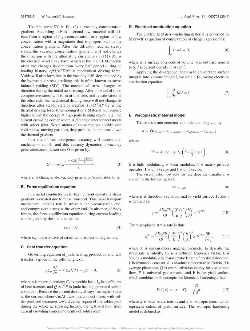
TABLE I. Material property for SAC405, aluminum and copper at 353 K.
Material properties SAC 405 Copper Aluminum
Vacancy relaxation time (s) 1:80� 103 (Ref. 56) 1:80� 10�3 1:80� 10�3
Effective charge number 10 (Ref. 57) 0.7 (Ref. 58) 4 (Ref. 59)
Grain boundary diffusivity (lm2/s) 2:72� 106 1:2� 103 (Ref. 60) 6:0� 103
Resistivity (Xm) 1:52� 10�7 1:678� 10�8 2:82� 10�8
Density (kg/m3) 7:39� 103 8:94� 103 2:70� 103
Thermal conductivity (W/(mK)) 57:3 4:16� 102 2:37� 102
Thermal expansion coefficient (K�1) 1:89� 10�6 1:65� 10�5 2:4� 10�5
Atomic volume (lm3) 2:71� 10�11 (Ref. 61) 1:19� 10�11 1:66� 10�11
Initial vacancy concentration (lm�3) 1:107� 106 (Ref. 62) 8:413� 103 6:02� 103 (Ref. 63)
Initial average grain size 1.0 1.0 1.0
Young’s modulus (GPa) 57.7 120.5 70
Poisson ratio 0.33 0.34 0.35
Linear kinematic hardening cons. (kg/m) 9:63� 109 (Ref. 29) 2:04� 109 7:4� 108
Nonlinear kinematic hardening cons. (kg/km) 7:25� 108 (Ref. 29) 1:8� 108 4:2� 106
Isotropic hardening cons. 383.3 (Ref. 35) 383.3 13.6
Creep activation energy (kgm2/s2mol) 7:95� 104 1:97� 105 (Ref. 64) 1:6� 105
063703-2 W. Yao and C. Basaran J. Appl. Phys. 111, 063703 (2012)
Downloaded 30 Jan 2013 to 67.20.205.34. Redistribution subject to AIP license or copyright; see http://jap.aip.org/about/rights_and_permissions
The first term rC in Eq. (2) is vacancy concentration
gradient. According to Fick’s second law, material will dif-
fuse from a region of high concentration to a region of low
concentration with a magnitude that is proportional to the
concentration gradient. After the diffusion reaches steady
states, the vacancy concentration gradient will not change
the direction with the alternating current. Z � e=kTðr;Þc is
the electron wind force term, which is the main EM mecha-
nism and changes its direction every half period during ac
loading history. cf X=kTrrsp is mechanical driving force.
Voids will also form due to the vacancy diffusion induced by
the hydrostatic stress gradient; this is often known as stress
induced voiding (SIV). The mechanical stress changes its
direction during the initial ac stressing. After a period of time,
compressive stress will form at one side, and tensile stress at
the other side; the mechanical driving force will not change its
direction after steady state is reached. ðc=kT2ÞQ�rT is the
thermal driving force (thermomigration). Material will acquire
higher kinematic energy at high joule heating region, e.g., the
current crowding corner where Al/Cu trace interconnect meets
with solder joint. When atoms of those regions collide with
colder slow-moving particles, they push the latter atoms down
the thermal gradient.
In a site of flux divergence, vacancy will accumulate,
nucleate or vanish, and this vacancy dynamics is vacancy
generation/annihilation rate G is given by:
G ¼ �Cv0
c� expð1�f ÞXrsp
kT
h iss
; (3)
where ss is characteristic vacancy generation/annihilation time.
B. Force equilibrium equation
In a metal conductor under high current density, a stress
gradient is created due to mass transport. This mass transport
mechanism induces tensile stress at the vacancy-rich end,
and compressive stress at the other end. In absence of body
forces, the force equilibrium equation during current loading
can be given by the static equation:
rij; j ¼ 0; (4)
where rij;j is derivative of stress with respect to degree of j.
C. Heat transfer equation
Governing equation of joule heating production and heat
transfer is given in the following text:
qCp@T
@t�rðkhrTÞ � qQ ¼ 0; (5)
where q is material density; Cp is specific heat; kh is coefficient
of heat transfer, and Q / I2R is joule heating generated within
conductor. Because the current density always has higher value
at the corners where Cu/Al trace interconnect meets with sol-
der joint and decreases toward center region of the solder joint
during the whole ac stressing history, the heat will flow from
current crowding corner into center of solder joint.
D. Electrical conduction equation
The electric field in a conducting material is governed by
Maxwell’s equation of conservation of charge expressed as:
ð�S
Jn dS ¼ 0; (6)
where S is surface of a control volume, n is outward normal
to S, J is current density in A=cm2.
Applying the divergence theorem to convert the surface
integral into volume integral, we obtain following electrical
conduction equation:
ð�V
@
@xJdV ¼ 0: (7)
E. Viscoplastic material model
The stress-strain constitutive model can be given by
r ¼ Hðetotal � eviscoplastic � ediffusion � ethermalÞ
where
H ¼ K1� 1þ 2l I � 1
31� 1
� �: (8)
K is bulk modulus, l is shear modulus, � is matrix product
operator, 1 is unit vector and I is unit vector.
The viscoplastic flow rule for rate dependent material is
shown in the following text:
_evp ¼ cn; (9)
where n is direction vector normal to yield surface F, and cis defined as:
c ¼ AD0Eb
khhFiE
� �n b
d
� �p
e�Q=Rh: (10)
The viscoplastic strain rate is thus
_evpij ¼
AD0Eb
kh
�hFiE
�n�b
d
�p
e�Q=Rh @F
@rij; (11)
where A is dimensionless material parameter to describe the
strain rate sensitivity, D0 is a diffusion frequency factor, E is
Young’s modulus, b is characteristic length of crystal dislocation,
k Boltzmann’s constant, h is absolute temperature in Kelvin, d is
average phase size, Q is creep activation energy for viscoplastic
flow, R is universal gas constant, and F is the yield surface,
which combined both isotropic and kinematic hardening effect:
Fðn; aÞ ¼ ks� Xk �ffiffiffi2
3
r�r; (12)
where X is back stress tensor, and r is isotropic stress which
represent radius of yield surface. The isotropic hardening
model is defined as:
063703-3 W. Yao and C. Basaran J. Appl. Phys. 111, 063703 (2012)
Downloaded 30 Jan 2013 to 67.20.205.34. Redistribution subject to AIP license or copyright; see http://jap.aip.org/about/rights_and_permissions
�rðaÞ ¼ffiffiffi2
3
rry0 þ R1½1� e�ca�; (13)
where ry0 is initial yield stress and R1 is isotropic hardening
saturation value.
The back stress tensor (kinematic hardening) is defined
as:
@X
@t¼ c
2
3H0ðaÞ n
knk ; (14)
where H0(a) is kinematic hardening modulus, c is expressed
in Eq. (11), n is effective stress, a is plastic strain given byÐ ffiffiffiffiffiffiffiffiffiffiffi23
_epij _e
pij
qdt.
F. Entropy damage model
Boltzmann’s equation gives the probability relationship
between entropy production and microscopic disorder as
follows:
s ¼ klnW; (15)
where k is Boltzmann’s constant, W is a disorder parameter
that gives the number of micro states corresponding to given
macro state. The relationship between entropy per unite
mass and the disorder parameter is given by Eq. (16):
s ¼ R
mslnW ¼ N0klnW; (16)
where R is universal gas constant, ms is specific mass, and
N0 is Avogadro’s constant. By some simple transformation,
the disorder function can be written as:
W ¼ e
s
N0k: (17)
Degradation metric is further defined as a ratio of change in
disorder parameter with respect to an initial disorder state as
follows:
D ¼ DcrW �W0
W0
¼ DcrDW
W0
¼ Dcr 1� e
s0 � s
N0k
0@
1A; (18)
where Dcr is the critical damage used to define failure or to
map degradation of a material property like elastic modulus
to damage parameter D. Entropy production during the EM
process is generated by several factors as shown in Eq. (19):
Ds ¼ðt
t0
�1
t2crT : rT þ CvDv
kT2F : Fþ 1
Tr : e
0vp
�dt; (19)
where ð1=t2ÞcrT : rT is joule heating generated entropy;
ðCvDv=kT2ÞF : F and ð1=TÞr : e0vp correspond to mass
diffusion and viscoplastic deformation produced entropy,
respectively.
By substituting Eq. (19) into (18), damage parameter
evolution can be given by:50
D¼Dcr 1� e
�Рt
t0
�1t2 crT :rTþ CvDv
kT2 F : Fþ 1T r : e
0vp
�dt
kN0
2666664
3777775;
(20)
where C is vacancy concentration, Cv is vacancy concentra-
tion, and Dv is effective diffusivity.
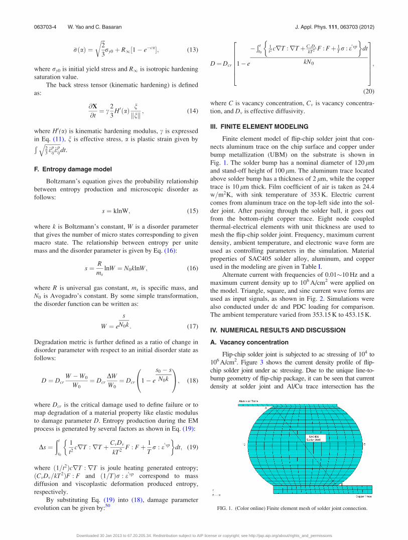
III. FINITE ELEMENT MODELING
Finite element model of flip-chip solder joint that con-
nects aluminum trace on the chip surface and copper under
bump metallization (UBM) on the substrate is shown in
Fig. 1. The solder bump has a nominal diameter of 120 lm
and stand-off height of 100 lm. The aluminum trace located
above solder bump has a thickness of 2 lm, while the copper
trace is 10 lm thick. Film coefficient of air is taken as 24.4
w=m2K, with sink temperature of 353 K. Electric current
comes from aluminum trace on the top-left side into the sol-
der joint. After passing through the solder ball, it goes out
from the bottom-right copper trace. Eight node coupled
thermal-electrical elements with unit thickness are used to
mesh the flip-chip solder joint. Frequency, maximum current
density, ambient temperature, and electronic wave form are
used as controlling parameters in the simulation. Material
properties of SAC405 solder alloy, aluminum, and copper
used in the modeling are given in Table I.
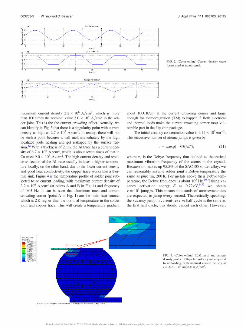
Alternate current with frequencies of 0.0110 Hz and a
maximum current density up to 106 A/cm2 were applied on
the model. Triangle, square, and sine current wave forms are
used as input signals, as shown in Fig. 2. Simulations were
also conducted under dc and PDC loading for comparison.
The ambient temperature varied from 353.15 K to 453.15 K.
IV. NUMERICAL RESULTS AND DISCUSSION
A. Vacancy concentration
Flip-chip solder joint is subjected to ac stressing of 104 to
106 A/cm2. Figure 3 shows the current density profile of flip-
chip solder joint under ac stressing. Due to the unique line-to-
bump geometry of flip-chip package, it can be seen that current
density at solder joint and Al/Cu trace intersection has the
FIG. 1. (Color online) Finite element mesh of solder joint connection.
063703-4 W. Yao and C. Basaran J. Appl. Phys. 111, 063703 (2012)
Downloaded 30 Jan 2013 to 67.20.205.34. Redistribution subject to AIP license or copyright; see http://jap.aip.org/about/rights_and_permissions
maximum current density 2:2� 106 A=cm2, which is more
than 100 times the nominal value 2:0� 104 A=cm2 in the sol-
der joint. This is the the current crowding effect. Actually, we
can identify in Fig. 3 that there is a singularity point with current
density as high as 2:7� 107 A=cm2. In reality, there will not
be such a point because it will melt immediately by the high
localized joule heating and get reshaped by the surface ten-
sion.52 With a thickness of 2lm, the Al trace has a current den-
sity of 6:7� 106 A=cm2, which is about seven times of that in
Cu trace 9:0� 105 A=cm2. The high current density and small
cross section of the Al trace usually induces a higher tempera-
ture locally; on the other hand, due to the lower current density
and good heat conductivity, the copper trace works like a ther-
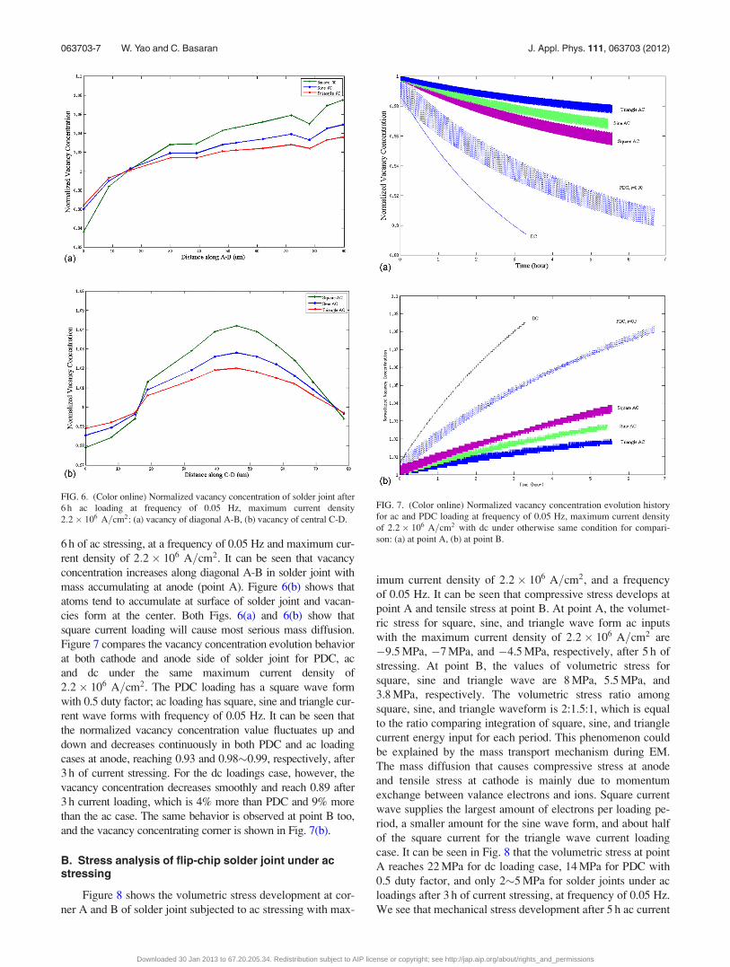
mal sink. Figure 4 is the temperature profile of solder joint sub-
jected to ac current loading, with maximum current density of
2:2� 106 A=cm2 (at points A and B in Fig. 1) and frequency
of 0.05 Hz. It can be seen that aluminum trace and current
crowding corner (point A in Fig. 1) are the main heat source,
which is 2 K higher than the nominal temperature in the solder
joint and copper trace. This will create a temperature gradient
about 1000 K/cm at the current crowding corner and large
enough for themomigration (TM) to happen.17 Both electrical
and thermal loads make the current crowding corner most vul-
nerable part in the flip-chip package.
The initial vacancy concentration value is 1:11� 107lm�3.
The successive number of atomic jumps is given by,
v ¼ v0expð�rE=kTÞ; (21)
where v0 is the Debye frequency that defined as theoretical
maximum vibration frequency of the atoms in the crystal.
Because tin makes up 95.5% of the SAC405 solder alloy, we
can reasonably assume solder joint’s Debye temperature the
same as pure tin, 200 K. For metals above their Debye tem-
perature, the Debye frequency is about 103 Hz.16 Taking va-
cancy activation energy E as 0.72 eV,9,52 we obtain
v ¼ 103 jump=s. This means thousands of atoms/vacancies
are expected to jump every second. Theoretically speaking,
the vacancy jump in current-reverse half cycle is the same as
the first half cycle; this should cancel each other. However,
FIG. 2. (Color online) Current density wave
forms used as input signal.
FIG. 3. (Color online) FEM mesh and current
density profile of flip-chip solder joint subjected
to ac loading, with nominal current density at
j ¼ 2:0� 104 sinð0:314tÞA=cm2.
063703-5 W. Yao and C. Basaran J. Appl. Phys. 111, 063703 (2012)
Downloaded 30 Jan 2013 to 67.20.205.34. Redistribution subject to AIP license or copyright; see http://jap.aip.org/about/rights_and_permissions
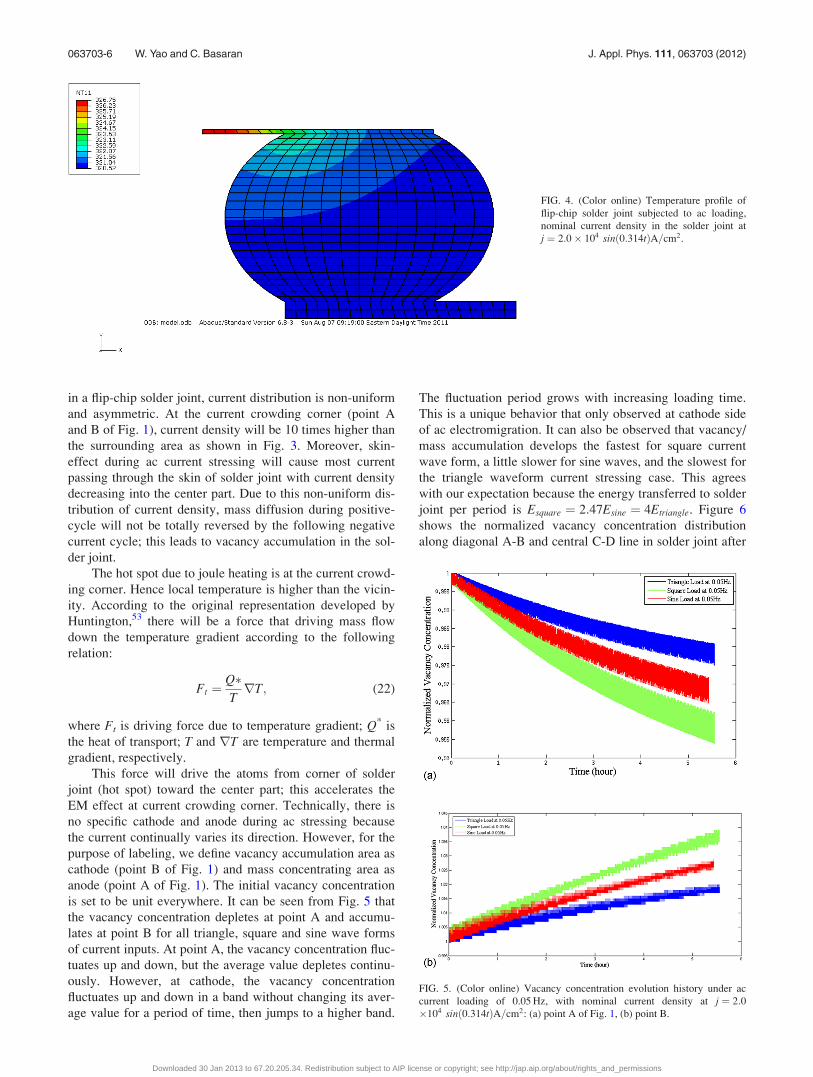
in a flip-chip solder joint, current distribution is non-uniform
and asymmetric. At the current crowding corner (point A
and B of Fig. 1), current density will be 10 times higher than
the surrounding area as shown in Fig. 3. Moreover, skin-
effect during ac current stressing will cause most current
passing through the skin of solder joint with current density
decreasing into the center part. Due to this non-uniform dis-
tribution of current density, mass diffusion during positive-
cycle will not be totally reversed by the following negative
current cycle; this leads to vacancy accumulation in the sol-
der joint.
The hot spot due to joule heating is at the current crowd-
ing corner. Hence local temperature is higher than the vicin-
ity. According to the original representation developed by
Huntington,53 there will be a force that driving mass flow
down the temperature gradient according to the following
relation:
Ft ¼Q�TrT; (22)
where Ft is driving force due to temperature gradient; Q* is
the heat of transport; T and rT are temperature and thermal
gradient, respectively.
This force will drive the atoms from corner of solder
joint (hot spot) toward the center part; this accelerates the
EM effect at current crowding corner. Technically, there is
no specific cathode and anode during ac stressing because
the current continually varies its direction. However, for the
purpose of labeling, we define vacancy accumulation area as
cathode (point B of Fig. 1) and mass concentrating area as
anode (point A of Fig. 1). The initial vacancy concentration
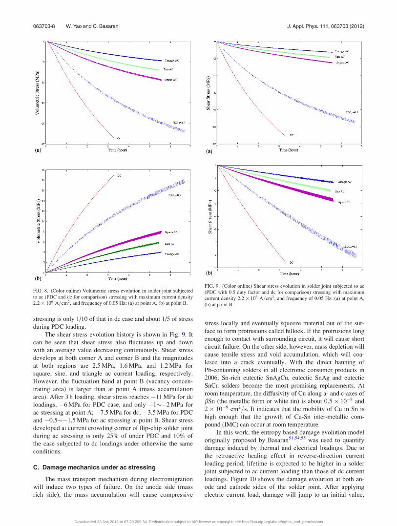
is set to be unit everywhere. It can be seen from Fig. 5 that
the vacancy concentration depletes at point A and accumu-
lates at point B for all triangle, square and sine wave forms
of current inputs. At point A, the vacancy concentration fluc-
tuates up and down, but the average value depletes continu-
ously. However, at cathode, the vacancy concentration
fluctuates up and down in a band without changing its aver-
age value for a period of time, then jumps to a higher band.
The fluctuation period grows with increasing loading time.
This is a unique behavior that only observed at cathode side
of ac electromigration. It can also be observed that vacancy/
mass accumulation develops the fastest for square current
wave form, a little slower for sine waves, and the slowest for
the triangle waveform current stressing case. This agrees
with our expectation because the energy transferred to solder
joint per period is Esquare ¼ 2:47Esine ¼ 4Etriangle. Figure 6
shows the normalized vacancy concentration distribution
along diagonal A-B and central C-D line in solder joint after
FIG. 4. (Color online) Temperature profile of
flip-chip solder joint subjected to ac loading,
nominal current density in the solder joint at
j ¼ 2:0� 104 sinð0:314tÞA=cm2.
FIG. 5. (Color online) Vacancy concentration evolution history under ac
current loading of 0.05 Hz, with nominal current density at j ¼ 2:0�104 sinð0:314tÞA=cm2: (a) point A of Fig. 1, (b) point B.
063703-6 W. Yao and C. Basaran J. Appl. Phys. 111, 063703 (2012)
Downloaded 30 Jan 2013 to 67.20.205.34. Redistribution subject to AIP license or copyright; see http://jap.aip.org/about/rights_and_permissions
6 h of ac stressing, at a frequency of 0.05 Hz and maximum cur-
rent density of 2:2� 106 A=cm2. It can be seen that vacancy
concentration increases along diagonal A-B in solder joint with
mass accumulating at anode (point A). Figure 6(b) shows that
atoms tend to accumulate at surface of solder joint and vacan-
cies form at the center. Both Figs. 6(a) and 6(b) show that
square current loading will cause most serious mass diffusion.
Figure 7 compares the vacancy concentration evolution behavior
at both cathode and anode side of solder joint for PDC, ac
and dc under the same maximum current density of
2:2� 106 A=cm2. The PDC loading has a square wave form
with 0.5 duty factor; ac loading has square, sine and triangle cur-
rent wave forms with frequency of 0.05 Hz. It can be seen that
the normalized vacancy concentration value fluctuates up and
down and decreases continuously in both PDC and ac loading
cases at anode, reaching 0.93 and 0.980.99, respectively, after
3 h of current stressing. For the dc loadings case, however, the
vacancy concentration decreases smoothly and reach 0.89 after
3 h current loading, which is 4% more than PDC and 9% more
than the ac case. The same behavior is observed at point B too,
and the vacancy concentrating corner is shown in Fig. 7(b).
B. Stress analysis of flip-chip solder joint under acstressing
Figure 8 shows the volumetric stress development at cor-
ner A and B of solder joint subjected to ac stressing with max-
imum current density of 2:2� 106 A=cm2, and a frequency
of 0.05 Hz. It can be seen that compressive stress develops at
point A and tensile stress at point B. At point A, the volumet-
ric stress for square, sine, and triangle wave form ac inputs
with the maximum current density of 2:2� 106 A=cm2 are
�9.5 MPa, �7 MPa, and �4.5 MPa, respectively, after 5 h of
stressing. At point B, the values of volumetric stress for
square, sine and triangle wave are 8 MPa, 5.5 MPa, and
3.8 MPa, respectively. The volumetric stress ratio among
square, sine, and triangle waveform is 2:1.5:1, which is equal
to the ratio comparing integration of square, sine, and triangle
current energy input for each period. This phenomenon could
be explained by the mass transport mechanism during EM.
The mass diffusion that causes compressive stress at anode
and tensile stress at cathode is mainly due to momentum
exchange between valance electrons and ions. Square current
wave supplies the largest amount of electrons per loading pe-
riod, a smaller amount for the sine wave form, and about half
of the square current for the triangle wave current loading
case. It can be seen in Fig. 8 that the volumetric stress at point
A reaches 22 MPa for dc loading case, 14 MPa for PDC with
0.5 duty factor, and only 25 MPa for solder joints under ac
loadings after 3 h of current stressing, at frequency of 0.05 Hz.
We see that mechanical stress development after 5 h ac current
FIG. 6. (Color online) Normalized vacancy concentration of solder joint after
6 h ac loading at frequency of 0.05 Hz, maximum current density
2:2� 106 A=cm2: (a) vacancy of diagonal A-B, (b) vacancy of central C-D.
FIG. 7. (Color online) Normalized vacancy concentration evolution history
for ac and PDC loading at frequency of 0.05 Hz, maximum current density
of 2:2� 106 A=cm2 with dc under otherwise same condition for compari-
son: (a) at point A, (b) at point B.
063703-7 W. Yao and C. Basaran J. Appl. Phys. 111, 063703 (2012)
Downloaded 30 Jan 2013 to 67.20.205.34. Redistribution subject to AIP license or copyright; see http://jap.aip.org/about/rights_and_permissions
stressing is only 1/10 of that in dc case and about 1/5 of stress
during PDC loading.
The shear stress evolution history is shown in Fig. 9. It
can be seen that shear stress also fluctuates up and down
with an average value decreasing continuously. Shear stress
develops at both corner A and corner B and the magnitudes
at both regions are 2.5 MPa, 1.6 MPa, and 1.2 MPa for
square, sine, and triangle ac current loading, respectively.
However, the fluctuation band at point B (vacancy concen-
trating area) is larger than at point A (mass accumulation
area). After 3 h loading, shear stress reaches �11 MPa for dc
loadings, �6 MPa for PDC case, and only �1�2 MPa for
ac stressing at point A; �7.5 MPa for dc, �3.5 MPa for PDC
and �0.5�1.5 MPa for ac stressing at point B. Shear stress
developed at current crowding corner of flip-chip solder joint
during ac stressing is only 25% of under PDC and 10% of
the case subjected to dc loadings under otherwise the same
conditions.
C. Damage mechanics under ac stressing
The mass transport mechanism during electromigration
will induce two types of failure. On the anode side (mass
rich side), the mass accumulation will cause compressive
stress locally and eventually squeeze material out of the sur-
face to form protrusions called hillock. If the protrusions long
enough to contact with surrounding circuit, it will cause short
circuit failure. On the other side, however, mass depletion will
cause tensile stress and void accumulation, which will coa-
lesce into a crack eventually. With the direct banning of
Pb-containing solders in all electronic consumer products in
2006, Sn-rich eutectic SnAgCu, eutectic SnAg and eutectic
SnCu solders become the most promising replacements. At
room temperature, the diffusivity of Cu along a- and c-axes of
bSn (the metallic form or white tin) is about 0:5� 10�8 and
2� 10�6 cm2=s. It indicates that the mobility of Cu in Sn is
high enough that the growth of Cu-Sn inter-metallic com-
pound (IMC) can occur at room temperature.
In this work, the entropy based damage evolution model
originally proposed by Basaran51,54,55 was used to quantify
damage induced by thermal and electrical loadings. Due to
the retroactive healing effect in reverse-direction current
loading period, lifetime is expected to be higher in a solder
joint subjected to ac current loading than those of dc current
loadings. Figure 10 shows the damage evolution at both an-
ode and cathode sides of the solder joint. After applying
electric current load, damage will jump to an initial value,
FIG. 8. (Color online) Volumetric stress evolution in solder joint subjected
to ac (PDC and dc for comparison) stressing with maximum current density
2:2� 106 A=cm2, and frequency of 0.05 Hz: (a) at point A, (b) at point B.
FIG. 9. (Color online) Shear stress evolution in solder joint subjected to ac
(PDC with 0.5 duty factor and dc for comparison) stressing with maximum
current density 2:2� 106 A=cm2, and frequency of 0.05 Hz: (a) at point A,
(b) at point B.
063703-8 W. Yao and C. Basaran J. Appl. Phys. 111, 063703 (2012)
Downloaded 30 Jan 2013 to 67.20.205.34. Redistribution subject to AIP license or copyright; see http://jap.aip.org/about/rights_and_permissions
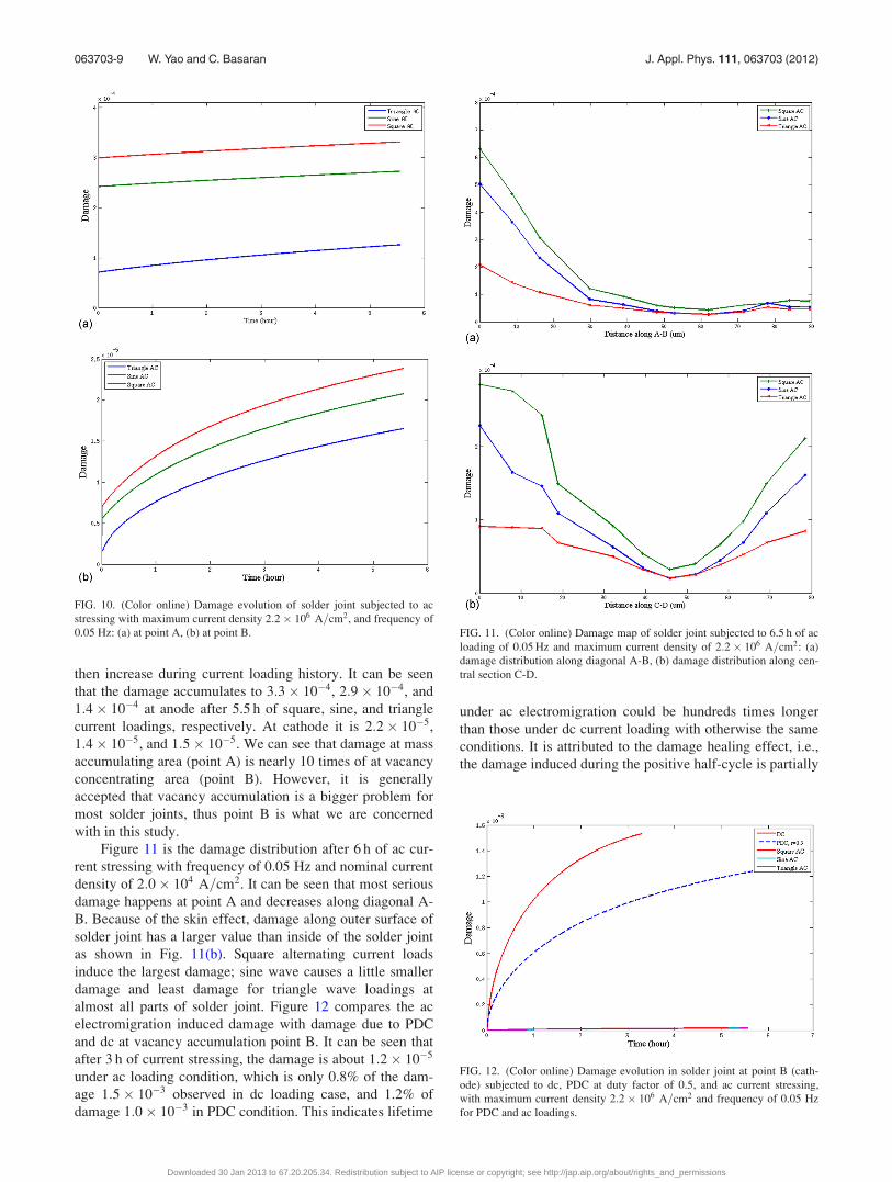
then increase during current loading history. It can be seen
that the damage accumulates to 3:3� 10�4, 2:9� 10�4, and
1:4� 10�4 at anode after 5.5 h of square, sine, and triangle
current loadings, respectively. At cathode it is 2:2� 10�5,
1:4� 10�5, and 1:5� 10�5. We can see that damage at mass
accumulating area (point A) is nearly 10 times of at vacancy
concentrating area (point B). However, it is generally
accepted that vacancy accumulation is a bigger problem for
most solder joints, thus point B is what we are concerned
with in this study.
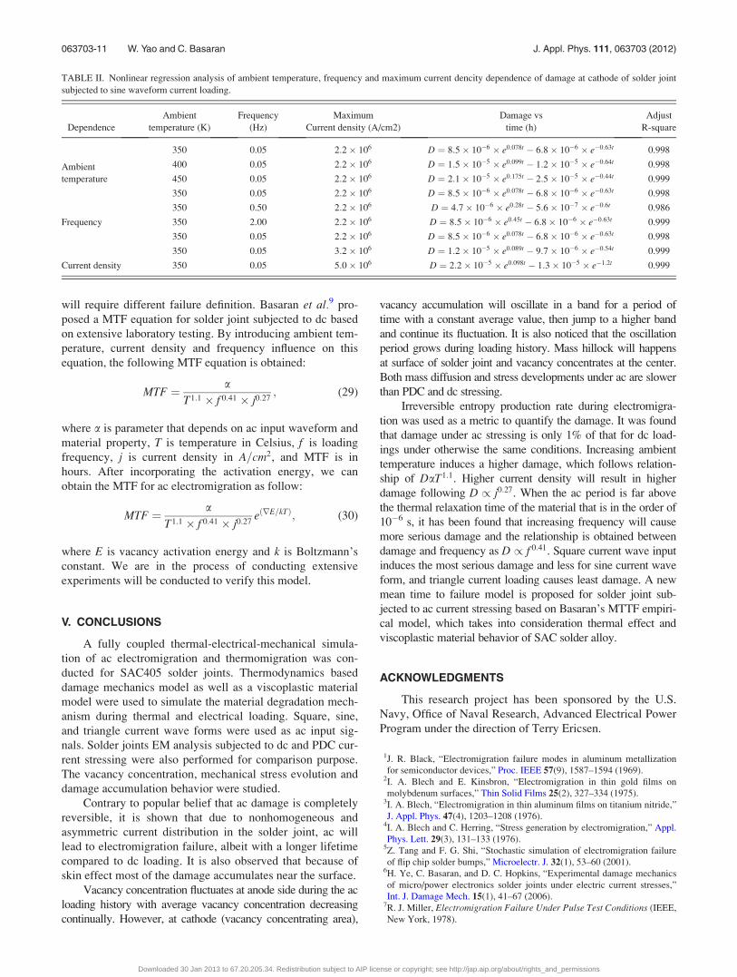
Figure 11 is the damage distribution after 6 h of ac cur-
rent stressing with frequency of 0.05 Hz and nominal current
density of 2:0� 104 A=cm2. It can be seen that most serious
damage happens at point A and decreases along diagonal A-
B. Because of the skin effect, damage along outer surface of
solder joint has a larger value than inside of the solder joint
as shown in Fig. 11(b). Square alternating current loads
induce the largest damage; sine wave causes a little smaller
damage and least damage for triangle wave loadings at
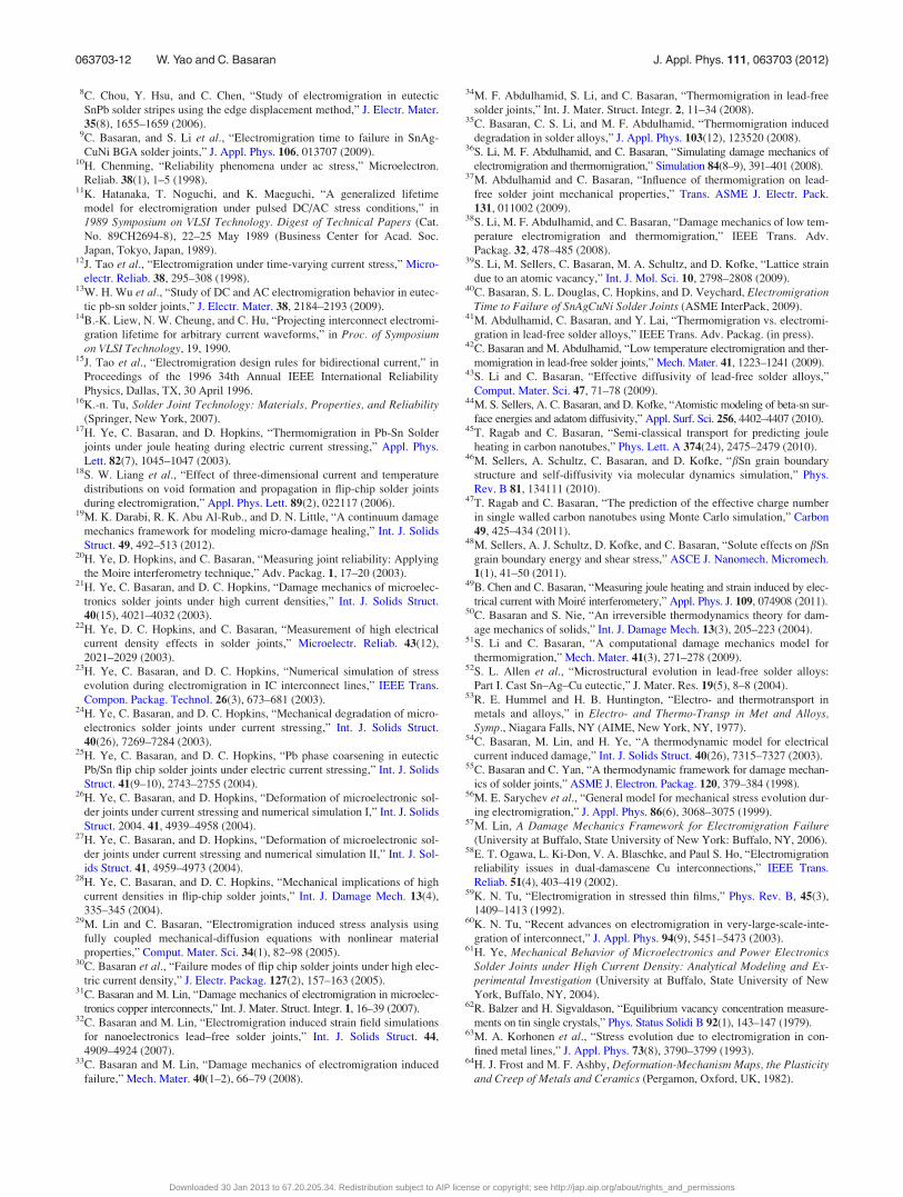
almost all parts of solder joint. Figure 12 compares the ac
electromigration induced damage with damage due to PDC
and dc at vacancy accumulation point B. It can be seen that
after 3 h of current stressing, the damage is about 1:2� 10�5
under ac loading condition, which is only 0.8% of the dam-
age 1:5� 10�3 observed in dc loading case, and 1.2% of
damage 1:0� 10�3 in PDC condition. This indicates lifetime
under ac electromigration could be hundreds times longer
than those under dc current loading with otherwise the same
conditions. It is attributed to the damage healing effect, i.e.,
the damage induced during the positive half-cycle is partially
FIG. 10. (Color online) Damage evolution of solder joint subjected to ac
stressing with maximum current density 2:2� 106 A=cm2, and frequency of
0.05 Hz: (a) at point A, (b) at point B. FIG. 11. (Color online) Damage map of solder joint subjected to 6.5 h of ac
loading of 0.05 Hz and maximum current density of 2:2� 106 A=cm2: (a)
damage distribution along diagonal A-B, (b) damage distribution along cen-
tral section C-D.
FIG. 12. (Color online) Damage evolution in solder joint at point B (cath-
ode) subjected to dc, PDC at duty factor of 0.5, and ac current stressing,
with maximum current density 2:2� 106 A=cm2 and frequency of 0.05 Hz
for PDC and ac loadings.
063703-9 W. Yao and C. Basaran J. Appl. Phys. 111, 063703 (2012)
Downloaded 30 Jan 2013 to 67.20.205.34. Redistribution subject to AIP license or copyright; see http://jap.aip.org/about/rights_and_permissions

healed during the following negative half-cycle current
stressing.
Figure 13 is the ambient temperature dependence of dam-
age evolution at cathode side of solder joint during ac current
stressing. It can be seen that higher ambient temperature induces
a larger initial damage as expected, and grows at a faster speed.
After 5 h of current stressing, damage reaches 4:9� 10�5 for
ambient temperature of 450 K, 2:5� 10�5 for ambient tempera-
ture of 400 K, and only 1:0� 10�5 for ambient temperature of
350 K. Figure 14 shows current density dependence of damage
of solder joint subjected to sine ac current loading at frequency
of 0.05 Hz. High current density will induce a high initial dam-
age and faster damage growth rate. Figure 15 is the ac current
frequency dependence of EM damage. It can be observed that
higher frequency results a larger initial damage and higher
growth rate.
The non-linear regression analysis of damage in the
SAC405 solder joint as a function of ambient temperature, fre-
quency, and maximum current density is shown in Table II with
an R-square value (confidence value, which means representa-
tive of data points) as large as 0.99. It has been found that the
ambient temperature, frequency, and current density dependence
of damage follows the following exponential model:
D ¼ a� ebt � c� e�dt; (23)
where D is the entropy production rate based material damage
metric; a–d are all positive parameters that depend on ambient
temperature, frequency, and maximum current density. For a
loading period long enough (over 6 h), the second part of the
above equation will be only 1% of the first part, thus we can
ignore the second parts’ influence, which will simplify the
preceding equation into the following representation:
D ¼ a� ebtbf bjt; (24)
where a is a general parameter that depends on current wave
form, ambient temperature, and frequency, bt is a temperature
exponent parameter, bf is a frequency exponent parameter, bj
is a current density exponent parameter, and t is current load-
ing time in hours. From Table II, it can be seen that the tem-
perature parameter bt grows with increasing temperature.
Non-linear regression gives us following relationship between
bt and temperature T in Celsius with R-square of 0.95:
bt ¼ 0:00052� T1:1: (25)
For constant ambient temperature at 350 K and frequency
of 0.05 Hz, relationship between bj and current density jin A=cm2 could be given as in Eq. (15) with a confidence
parameter of 0.98:
bj ¼ 0:0015� j0:27: (26)
By following the same procedure, we obtain the following
relationship between ac frequency f and parameter bf with a
confidence parameter R-square as 0.985:
bf ¼ 0:344� f 0:41: (27)
By combing all three parameters together, we obtain the EM
and TM damage model of solder joint under ac current
stressing as:
D ¼ a� ebT1:1f 0:41j0:27t: (28)
We further define the failure of solder joint when D¼ 0.01 in
this study for simplicity. We realize that different application
FIG. 13. (Color online) Temperature dependence of damage evolution in
solder joint at point B (cathode) subjected to ac current stressing, with maxi-
mum current density 2:2� 106 A=cm2 and frequency of 0.05 Hz.
FIG. 14. (Color online) Current density dependence of damage evolution of
solder joint at point B (cathode) subjected to ac current stressing, with ambi-
ent temperature at 350 K and frequency of 0.05 Hz.
FIG. 15. (Color online) Frequency dependence of damage evolution of sol-
der joint at point B (cathode) subjected to ac current stressing, with maxi-
mum current density 2:2� 106 A=cm2 and frequency of 0.05 Hz.
063703-10 W. Yao and C. Basaran J. Appl. Phys. 111, 063703 (2012)
Downloaded 30 Jan 2013 to 67.20.205.34. Redistribution subject to AIP license or copyright; see http://jap.aip.org/about/rights_and_permissions
will require different failure definition. Basaran et al.9 pro-
posed a MTF equation for solder joint subjected to dc based
on extensive laboratory testing. By introducing ambient tem-
perature, current density and frequency influence on this
equation, the following MTF equation is obtained:
MTF ¼ aT1:1 � f 0:41 � j0:27
; (29)
where a is parameter that depends on ac input waveform and
material property, T is temperature in Celsius, f is loading
frequency, j is current density in A=cm2, and MTF is in
hours. After incorporating the activation energy, we can
obtain the MTF for ac electromigration as follow:
MTF ¼ aT1:1 � f 0:41 � j0:27
eðrE=kTÞ; (30)
where E is vacancy activation energy and k is Boltzmann’s
constant. We are in the process of conducting extensive
experiments will be conducted to verify this model.
V. CONCLUSIONS
A fully coupled thermal-electrical-mechanical simula-
tion of ac electromigration and thermomigration was con-
ducted for SAC405 solder joints. Thermodynamics based
damage mechanics model as well as a viscoplastic material
model were used to simulate the material degradation mech-
anism during thermal and electrical loading. Square, sine,
and triangle current wave forms were used as ac input sig-
nals. Solder joints EM analysis subjected to dc and PDC cur-
rent stressing were also performed for comparison purpose.
The vacancy concentration, mechanical stress evolution and
damage accumulation behavior were studied.
Contrary to popular belief that ac damage is completely
reversible, it is shown that due to nonhomogeneous and
asymmetric current distribution in the solder joint, ac will
lead to electromigration failure, albeit with a longer lifetime
compared to dc loading. It is also observed that because of
skin effect most of the damage accumulates near the surface.
Vacancy concentration fluctuates at anode side during the ac
loading history with average vacancy concentration decreasing
continually. However, at cathode (vacancy concentrating area),
vacancy accumulation will oscillate in a band for a period of
time with a constant average value, then jump to a higher band
and continue its fluctuation. It is also noticed that the oscillation
period grows during loading history. Mass hillock will happens
at surface of solder joint and vacancy concentrates at the center.
Both mass diffusion and stress developments under ac are slower
than PDC and dc stressing.
Irreversible entropy production rate during electromigra-
tion was used as a metric to quantify the damage. It was found
that damage under ac stressing is only 1% of that for dc load-
ings under otherwise the same conditions. Increasing ambient
temperature induces a higher damage, which follows relation-
ship of DaT1:1. Higher current density will result in higher
damage following D / j0:27. When the ac period is far above
the thermal relaxation time of the material that is in the order of
10�6 s, it has been found that increasing frequency will cause
more serious damage and the relationship is obtained between
damage and frequency as D / f 0:41. Square current wave input
induces the most serious damage and less for sine current wave
form, and triangle current loading causes least damage. A new
mean time to failure model is proposed for solder joint sub-
jected to ac current stressing based on Basaran’s MTTF empiri-
cal model, which takes into consideration thermal effect and
viscoplastic material behavior of SAC solder alloy.
ACKNOWLEDGMENTS
This research project has been sponsored by the U.S.
Navy, Office of Naval Research, Advanced Electrical Power
Program under the direction of Terry Ericsen.
1J. R. Black, “Electromigration failure modes in aluminum metallization
for semiconductor devices,” Proc. IEEE 57(9), 1587–1594 (1969).2I. A. Blech and E. Kinsbron, “Electromigration in thin gold films on
molybdenum surfaces,” Thin Solid Films 25(2), 327–334 (1975).3I. A. Blech, “Electromigration in thin aluminum films on titanium nitride,”
J. Appl. Phys. 47(4), 1203–1208 (1976).4I. A. Blech and C. Herring, “Stress generation by electromigration,” Appl.
Phys. Lett. 29(3), 131–133 (1976).5Z. Tang and F. G. Shi, “Stochastic simulation of electromigration failure
of flip chip solder bumps,” Microelectr. J. 32(1), 53–60 (2001).6H. Ye, C. Basaran, and D. C. Hopkins, “Experimental damage mechanics
of micro/power electronics solder joints under electric current stresses,”
Int. J. Damage Mech. 15(1), 41–67 (2006).7R. J. Miller, Electromigration Failure Under Pulse Test Conditions (IEEE,
New York, 1978).
TABLE II. Nonlinear regression analysis of ambient temperature, frequency and maximum current dencity dependence of damage at cathode of solder joint
subjected to sine waveform current loading.
Dependence
Ambient
temperature (K)
Frequency
(Hz)
Maximum
Current density (A/cm2)
Damage vs
time (h)
Adjust
R-square
Ambient
temperature
350 0.05 2:2� 106 D ¼ 8:5� 10�6 � e0:078t � 6:8� 10�6 � e�0:63t 0.998
400 0.05 2:2� 106 D ¼ 1:5� 10�5 � e0:099t � 1:2� 10�5 � e�0:64t 0.998
450 0.05 2:2� 106 D ¼ 2:1� 10�5 � e0:175t � 2:5� 10�5 � e�0:44t 0.999
Frequency
350 0.05 2:2� 106 D ¼ 8:5� 10�6 � e0:078t � 6:8� 10�6 � e�0:63t 0.998
350 0.50 2:2� 106 D ¼ 4:7� 10�6 � e0:28t � 5:6� 10�7 � e�0:6t 0.986
350 2.00 2:2� 106 D ¼ 8:5� 10�6 � e0:45t � 6:8� 10�6 � e�0:63t 0.999
Current density
350 0.05 2:2� 106 D ¼ 8:5� 10�6 � e0:078t � 6:8� 10�6 � e�0:63t 0.998
350 0.05 3:2� 106 D ¼ 1:2� 10�5 � e0:089t � 9:7� 10�6 � e�0:54t 0.999
350 0.05 5:0� 106 D ¼ 2:2� 10�5 � e0:098t � 1:3� 10�5 � e�1:2t 0.999
063703-11 W. Yao and C. Basaran J. Appl. Phys. 111, 063703 (2012)
Downloaded 30 Jan 2013 to 67.20.205.34. Redistribution subject to AIP license or copyright; see http://jap.aip.org/about/rights_and_permissions
8C. Chou, Y. Hsu, and C. Chen, “Study of electromigration in eutectic
SnPb solder stripes using the edge displacement method,” J. Electr. Mater.
35(8), 1655–1659 (2006).9C. Basaran, and S. Li et al., “Electromigration time to failure in SnAg-
CuNi BGA solder joints,” J. Appl. Phys. 106, 013707 (2009).10H. Chenming, “Reliability phenomena under ac stress,” Microelectron.
Reliab. 38(1), 1–5 (1998).11K. Hatanaka, T. Noguchi, and K. Maeguchi, “A generalized lifetime
model for electromigration under pulsed DC/AC stress conditions,” in
1989 Symposium on VLSI Technology. Digest of Technical Papers (Cat.
No. 89CH2694-8), 22–25 May 1989 (Business Center for Acad. Soc.
Japan, Tokyo, Japan, 1989).12J. Tao et al., “Electromigration under time-varying current stress,” Micro-
electr. Reliab. 38, 295–308 (1998).13W. H. Wu et al., “Study of DC and AC electromigration behavior in eutec-
tic pb-sn solder joints,” J. Electr. Mater. 38, 2184–2193 (2009).14B.-K. Liew, N. W. Cheung, and C. Hu, “Projecting interconnect electromi-
gration lifetime for arbitrary current waveforms,” in Proc. of Symposiumon VLSI Technology, 19, 1990.
15J. Tao et al., “Electromigration design rules for bidirectional current,” in
Proceedings of the 1996 34th Annual IEEE International Reliability
Physics, Dallas, TX, 30 April 1996.16K.-n. Tu, Solder Joint Technology: Materials, Properties, and Reliability
(Springer, New York, 2007).17H. Ye, C. Basaran, and D. Hopkins, “Thermomigration in Pb-Sn Solder
joints under joule heating during electric current stressing,” Appl. Phys.
Lett. 82(7), 1045–1047 (2003).18S. W. Liang et al., “Effect of three-dimensional current and temperature
distributions on void formation and propagation in flip-chip solder joints
during electromigration,” Appl. Phys. Lett. 89(2), 022117 (2006).19M. K. Darabi, R. K. Abu Al-Rub., and D. N. Little, “A continuum damage
mechanics framework for modeling micro-damage healing,” Int. J. Solids
Struct. 49, 492–513 (2012).20H. Ye, D. Hopkins, and C. Basaran, “Measuring joint reliability: Applying
the Moire interferometry technique,” Adv. Packag. 1, 17–20 (2003).21H. Ye, C. Basaran, and D. C. Hopkins, “Damage mechanics of microelec-
tronics solder joints under high current densities,” Int. J. Solids Struct.
40(15), 4021–4032 (2003).22H. Ye, D. C. Hopkins, and C. Basaran, “Measurement of high electrical
current density effects in solder joints,” Microelectr. Reliab. 43(12),
2021–2029 (2003).23H. Ye, C. Basaran, and D. C. Hopkins, “Numerical simulation of stress
evolution during electromigration in IC interconnect lines,” IEEE Trans.
Compon. Packag. Technol. 26(3), 673–681 (2003).24H. Ye, C. Basaran, and D. C. Hopkins, “Mechanical degradation of micro-
electronics solder joints under current stressing,” Int. J. Solids Struct.
40(26), 7269–7284 (2003).25H. Ye, C. Basaran, and D. C. Hopkins, “Pb phase coarsening in eutectic
Pb/Sn flip chip solder joints under electric current stressing,” Int. J. Solids
Struct. 41(9–10), 2743–2755 (2004).26H. Ye, C. Basaran, and D. Hopkins, “Deformation of microelectronic sol-
der joints under current stressing and numerical simulation I,” Int. J. Solids
Struct. 2004. 41, 4939–4958 (2004).27H. Ye, C. Basaran, and D. Hopkins, “Deformation of microelectronic sol-
der joints under current stressing and numerical simulation II,” Int. J. Sol-
ids Struct. 41, 4959–4973 (2004).28H. Ye, C. Basaran, and D. C. Hopkins, “Mechanical implications of high
current densities in flip-chip solder joints,” Int. J. Damage Mech. 13(4),
335–345 (2004).29M. Lin and C. Basaran, “Electromigration induced stress analysis using
fully coupled mechanical-diffusion equations with nonlinear material
properties,” Comput. Mater. Sci. 34(1), 82–98 (2005).30C. Basaran et al., “Failure modes of flip chip solder joints under high elec-
tric current density,” J. Electr. Packag. 127(2), 157–163 (2005).31C. Basaran and M. Lin, “Damage mechanics of electromigration in microelec-
tronics copper interconnects,” Int. J. Mater. Struct. Integr. 1, 16–39 (2007).32C. Basaran and M. Lin, “Electromigration induced strain field simulations
for nanoelectronics lead–free solder joints,” Int. J. Solids Struct. 44,
4909–4924 (2007).33C. Basaran and M. Lin, “Damage mechanics of electromigration induced
failure,” Mech. Mater. 40(1–2), 66–79 (2008).
34M. F. Abdulhamid, S. Li, and C. Basaran, “Thermomigration in lead-free
solder joints,” Int. J. Mater. Struct. Integr. 2, 11–34 (2008).35C. Basaran, C. S. Li, and M. F. Abdulhamid, “Thermomigration induced
degradation in solder alloys,” J. Appl. Phys. 103(12), 123520 (2008).36S. Li, M. F. Abdulhamid, and C. Basaran, “Simulating damage mechanics of
electromigration and thermomigration,” Simulation 84(8–9), 391–401 (2008).37M. Abdulhamid and C. Basaran, “Influence of thermomigration on lead-
free solder joint mechanical properties,” Trans. ASME J. Electr. Pack.
131, 011002 (2009).38S. Li, M. F. Abdulhamid, and C. Basaran, “Damage mechanics of low tem-
perature electromigration and thermomigration,” IEEE Trans. Adv.
Packag. 32, 478–485 (2008).39S. Li, M. Sellers, C. Basaran, M. A. Schultz, and D. Kofke, “Lattice strain
due to an atomic vacancy,” Int. J. Mol. Sci. 10, 2798–2808 (2009).40C. Basaran, S. L. Douglas, C. Hopkins, and D. Veychard, Electromigration
Time to Failure of SnAgCuNi Solder Joints (ASME InterPack, 2009).41M. Abdulhamid, C. Basaran, and Y. Lai, “Thermomigration vs. electromi-
gration in lead-free solder alloys,” IEEE Trans. Adv. Packag. (in press).42C. Basaran and M. Abdulhamid, “Low temperature electromigration and ther-
momigration in lead-free solder joints,” Mech. Mater. 41, 1223–1241 (2009).43S. Li and C. Basaran, “Effective diffusivity of lead-free solder alloys,”
Comput. Mater. Sci. 47, 71–78 (2009).44M. S. Sellers, A. C. Basaran, and D. Kofke, “Atomistic modeling of beta-sn sur-
face energies and adatom diffusivity,” Appl. Surf. Sci. 256, 4402–4407 (2010).45T. Ragab and C. Basaran, “Semi-classical transport for predicting joule
heating in carbon nanotubes,” Phys. Lett. A 374(24), 2475–2479 (2010).46M. Sellers, A. Schultz, C. Basaran, and D. Kofke, “bSn grain boundary
structure and self-diffusivity via molecular dynamics simulation,” Phys.
Rev. B 81, 134111 (2010).47T. Ragab and C. Basaran, “The prediction of the effective charge number
in single walled carbon nanotubes using Monte Carlo simulation,” Carbon
49, 425–434 (2011).48M. Sellers, A. J. Schultz, D. Kofke, and C. Basaran, “Solute effects on bSn
grain boundary energy and shear stress,” ASCE J. Nanomech. Micromech.
1(1), 41–50 (2011).49B. Chen and C. Basaran, “Measuring joule heating and strain induced by elec-
trical current with Moire interferometery,” Appl. Phys. J. 109, 074908 (2011).50C. Basaran and S. Nie, “An irreversible thermodynamics theory for dam-
age mechanics of solids,” Int. J. Damage Mech. 13(3), 205–223 (2004).51S. Li and C. Basaran, “A computational damage mechanics model for
thermomigration,” Mech. Mater. 41(3), 271–278 (2009).52S. L. Allen et al., “Microstructural evolution in lead-free solder alloys:
Part I. Cast Sn–Ag–Cu eutectic,” J. Mater. Res. 19(5), 8–8 (2004).53R. E. Hummel and H. B. Huntington, “Electro- and thermotransport in
metals and alloys,” in Electro- and Thermo-Transp in Met and Alloys,Symp., Niagara Falls, NY (AIME, New York, NY, 1977).
54C. Basaran, M. Lin, and H. Ye, “A thermodynamic model for electrical
current induced damage,” Int. J. Solids Struct. 40(26), 7315–7327 (2003).55C. Basaran and C. Yan, “A thermodynamic framework for damage mechan-
ics of solder joints,” ASME J. Electron. Packag. 120, 379–384 (1998).56M. E. Sarychev et al., “General model for mechanical stress evolution dur-
ing electromigration,” J. Appl. Phys. 86(6), 3068–3075 (1999).57M. Lin, A Damage Mechanics Framework for Electromigration Failure
(University at Buffalo, State University of New York: Buffalo, NY, 2006).58E. T. Ogawa, L. Ki-Don, V. A. Blaschke, and Paul S. Ho, “Electromigration
reliability issues in dual-damascene Cu interconnections,” IEEE Trans.
Reliab. 51(4), 403–419 (2002).59K. N. Tu, “Electromigration in stressed thin films,” Phys. Rev. B, 45(3),
1409–1413 (1992).60K. N. Tu, “Recent advances on electromigration in very-large-scale-inte-
gration of interconnect,” J. Appl. Phys. 94(9), 5451–5473 (2003).61H. Ye, Mechanical Behavior of Microelectronics and Power Electronics
Solder Joints under High Current Density: Analytical Modeling and Ex-perimental Investigation (University at Buffalo, State University of New
York, Buffalo, NY, 2004).62R. Balzer and H. Sigvaldason, “Equilibrium vacancy concentration measure-
ments on tin single crystals,” Phys. Status Solidi B 92(1), 143–147 (1979).63M. A. Korhonen et al., “Stress evolution due to electromigration in con-
fined metal lines,” J. Appl. Phys. 73(8), 3790–3799 (1993).64H. J. Frost and M. F. Ashby, Deformation-Mechanism Maps, the Plasticity
and Creep of Metals and Ceramics (Pergamon, Oxford, UK, 1982).
063703-12 W. Yao and C. Basaran J. Appl. Phys. 111, 063703 (2012)
Downloaded 30 Jan 2013 to 67.20.205.34. Redistribution subject to AIP license or copyright; see http://jap.aip.org/about/rights_and_permissions