Characterization of Planar Lead Halide Perovskite Solar Cells by ...

The Pennsylvania State University
The Graduate School
College of Earth and Mineral Sciences
ELECTROMECHANICAL CHARACTERIZATION OF LEAD MAGNESIUM
NIOBATE BASED THIN FILMS
A Dissertation in
Materials Science and Engineering
by
Smitha Shetty
© 2019 Smitha Shetty
Submitted in Partial Fulfillment
of the Requirements
for the Degree of
Doctor of Philosophy
May 2019

The dissertation of Smitha Shetty was reviewed and approved* by the following:
Susan Trolier-McKinstry
Professor of Ceramic Science and Engineering and Electrical Engineering
Dissertation Adviser
Chair of Committee
Clive A. Randall
Professor of Materials Science and Engineering
Venkatraman Gopalan
Professor, Materials Science and Engineering and Engineering Science and
Mechanics
Chris Giebink
Assistant Professor of Electrical Engineering
Tom Shaw
IBM
Special Member
Suzanne Mohney
Professor of Materials Science and Engineering and Electrical Engineering Chair,
Intercollege Graduate Degree Program in Materials Science and Engineering
*Signatures are on file in the Graduate School

iii
ABSTRACT
Lead Magnesium Niobate (PMN) is the most studied relaxor ferroelectric compound with
cation order intimately interacting with nanoscale polar heterogeneities. In undoped bulk PMN, the
cation order can hardly be changed, while the polar order is quite responsive to external stimuli
(electric field and temperature). Moreover, PMN-based oxides are of technological importance,
displaying strong piezoelectric effects, high electrostrictive strains, and unusually high dielectric
permittivity. The local compositional heterogeneity associated with short-range ordering of Mg and
Nb in PbMg1/3Nb2/3O3 (PMN) is correlated with its characteristic relaxor ferroelectric behavior.
Fully-ordered PMN has not been prepared as a bulk material.
This work reports the growth and characterization of thin film PMN heterostructures with
long-range cation order. These films were grown at temperatures below 1073 K by artificially
reducing the degree of disorder via synthesis of heterostructures with alternate layers of
Pb(Mg2/3Nb1/3)O3 and PbNbO3, as suggested by the random-site model. 100-nm-thick, phase-pure
films were grown epitaxially on (111) SrTiO3 substrates using alternate target timed pulsed-laser
deposition of Pb(Mg2/3Nb1/3)O3 and PbNbO3 targets with 20% excess Pb. Selected area electron
diffraction confirmed the emergence of (1/2, 1/2, 1/2) superlattice spots with randomly distributed
ordered domains as large as ~150 nm. These heterostructures exhibited a dielectric constant of 800,
loss tangents of ~0.03 and 2 x remanent polarization of ~11 μC/cm2 at room temperature.
Polarization-electric field hysteresis loops, Rayleigh data, and optical second-harmonic generation
measurements are consistent with the development of ferroelectric domains below 140 K.
Temperature-dependent permittivity measurements demonstrate reduced frequency dispersion
compared to short range ordered PMN films. Although perfectly layered heterostructures could not
be grown, the novelty of this work lies in achieving the highest cation order in PMN. Further, these
engineered films exhibit a continuum between normal and relaxor ferroelectric behavior as a

iv
function of temperature.
The dynamic nonlinear dielectric responses were also studied as a function of temperature and
electric field for the PMN thin films with long- and short-range ordering. It was found that long-
range ordering decreased the dispersion in the first and third harmonic displacement current relative
to short-range ordered films. For both sets of films, a second harmonic component of the dielectric
response was also detected. The phase angles of the higher harmonic responses were used to probe
the continuum in ferroelectric- relaxor behavior in these films. At high temperatures (e.g. above
the freezing temperature), the presence of nanopolar clusters is believed to cause the strong
dispersion in the third harmonic response in both long range and short-range films. However, at
lower temperatures, changes in the sign of χ3 suggest long-range ferroelectric ordering, such that
the response of mobile interfaces (believed to be domain walls) dominate the response.
Additionally, miniaturization of PMN based ferroelectric films for actuator applications
necessitates quantification of piezoelectric properties with scaling. A single beam
laser interferometer based on a modified Mirau detection scheme with a vertical resolution of
∼5 pm was developed for localized d33 measurements on patterned piezoelectric films. The tool
provides high spatial resolution (∼2 μm), essential for understanding scaling and processing effects
in piezoelectric materials. This approach enables quantitative information on d33, currently difficult
in local measurement techniques such as piezoresponse force microscopy. The interferometer is
built in a custom microscope and employs a phase lock-in technique in order to detect sub-
Angstrom displacements. d33 measurements on single crystal 0.67PbMg0.33Nb0.67O3-
0.33PbTiO3 and bulk PbZrTiO3-5A ceramics demonstrated agreement within <3%
with measurements using a double beam laser interferometer. Substrate bending contributions to
out-of-plane strain, observed in thin continuous PbZr0.52Ti0.48O3 films grown on Si substrates is
reduced for electrode diameters smaller than 100 μm. Direct scanning across 5 μm and 10 μm

v
features etched in 0.5 μm thick PbZr0.52Ti0.48O3 films doped with 1% Nb poled at either room
temperature or 150 °C confirmed minimal substrate contributions to the effective d33,f. Furthermore,
enhanced d33,f values were observed along the feature edges due to partial declamping from the
substrate, thus validating the application of single beam interferometry on finely
patterned electrodes.

vi
TABLE OF CONTENTS
LIST OF FIGURES ................................................................................................................. viii
LIST OF TABLES ................................................................................................................... xiii
ACKNOWLEDGEMENTS ..................................................................................................... xiv
Chapter 1 Introduction and thesis organization ...................................................................... 1
1.1 Introduction ........................................................................................................ 1 1.2 Thesis Organization ............................................................................................ 3
Chapter 2 Literature Review ................................................................................................... 5
2.1 Introduction to lead magnesium niobate (PMN) and relaxor ferroelectricity .... 5 2.2 Rayleigh analysis: probing nonlinearity in normal ferroelectric and relaxor
ferroelectric thin films ...................................................................................... 16 2.3 Role of substrate clamping in thin ferroelectric films ........................................ 19
Chapter 3 Relaxor behavior in ordered lead magnesium niobate (PbMg1/3Nb2/3O3) thin
films ................................................................................................................................. 21
3.1 Introduction ........................................................................................................ 21 3.2 Experimental procedure ..................................................................................... 22 3.3 Results and discussion ........................................................................................ 25
Chapter 4 Non-linearity in engineered lead magnesium niobate (PbMg1/3Nb2/3O3) thin
films ................................................................................................................................. 41
4.1 Introduction to non-linear susceptibility in relaxor ferroelectricity ................... 41 4.2 Experimental procedure ..................................................................................... 45 4.3 Results and discussion ........................................................................................ 46
Chapter 5 Quantitative and high spatial resolution d33 measurement of piezoelectric bulk
and thin films ................................................................................................................... 55
5.1 Introduction ........................................................................................................ 55 5.2 Experimental procedure ..................................................................................... 60 5.3 Results and discussion ........................................................................................ 66
Chapter 6 .................................................................................................................................. Conclusion and future work ............................................................................................. 75
6.1 Conclusions ........................................................................................................ 75

vii
6.2 Future work ...................................................................................................... 77
Appendices ............................................................................................................................... 86
Appendix A: RHEED assisted growth of PbMg2/3Nb1/3O3-PbNbO3
heterostructure films ......................................................................................... 87 Appendix B: Growth of heterostructure PMN thin films on different substrates .... 90
References ................................................................................................................................ 94

viii
LIST OF FIGURES
Figure 1-1 Schematic of piezoelectronic transistor proposed by IBM11 .................................. 2
Figure 2-1: Comparison between normal and relaxor ferroelectrics19. .................................... 6
Figure 2-2: Electric-field —temperature phase diagram for PMN obtained in the FC
regime (E parallel to <111>29) where FE: ferroelectric phase, GL: glassy phase and
PE: paraelectric phase in PMN. ....................................................................................... 8
Figure 2-3: Classification of complex lead based perovskites on the basis of B-site
ordering and dielectric behavior36. ................................................................................... 10
Figure 2-4: Influence of long range ordering in PST obtained after annealing on (a) size
of chemically ordered regions and (b) dielectric behavior37,44. ........................................ 11
Figure 2-5: Temperature dependence of correlation lengths from neutron scattering of
PMN at Tf with insert showing fitting to Vogel Fulcher, indicating glassy behavior5..... 14
Figure 2-6: Schematic showing nucleation, growth and interaction of polar nanoregions
in COR regions in a paraelectric matrix as a function of temperature. ............................ 14
Figure 2-7:(a) Temperature dependence of the dielectric permittivity of PMN ceramic
with increasing PT as a function of frequency. (b)Temperature dependence of the
reciprocal of dielectric permittivity for PMN ceramic with increasing PT (<36%),
where the straight lines reveal that the dielectric responses of PMN-PT ceramics
start to follow Curie–Weiss law at the temperature much higher than Tmax for PMN. .... 16
Figure 2-8: Potential energy landscape for domain wall motion in an environment with
randomly distributed pinning centers75 ............................................................................ 17
Figure 3-1: Proposed PMN heterostructure with alternate PbNbO3 and PbMg
2/3Nb
1/3O
3
layering along <111> ....................................................................................................... 22
Figure 3-2: (a) XRD pattern for long range ordered PMN heterostructure film grown on
001 and 111 STO (labelled as PMNLRO)and short range ordered PMN on 111 STO
(labelled as PMNSRO) (b) ω-scan for 111 reflection on 30 nm PMN heterostructure
film grown on STO. ......................................................................................................... 26
Figure 3-3: (a) Simulated data fit to the experimental data on the long range ordered
PMN heterostructure film obtained by Rutherfold Backscattering (b) Calculated
elemental composition from simulation. .......................................................................... 26
Figure 3-4:(a) A cross-section TEM image of a long range ordered heterostructure PMN
(111) film (marked LRO-PMN) on LSMO/STO (111) recorded along the [−112]
pole (b) FFT from a high resolution TEM image (INSET) showing superstructure
reflections; (c)(d) (e) cross-sectional dark field images captured using one of the

ix
superstructure reflections in (b), revealing the highlighted cation-ordered domain in
the film. ............................................................................................................................ 28
Figure 3-5:(a) A cross-section TEM image pattern of a short range ordered PMN (111)
film (marked SRO-PMN) on LSMO/STO (111) (b) FFT of a high resolution TEM
image recorded along the [−112] pole showing diffused superstructure reflections
(marked by blue circles) associated with short-range cation ordering; (c) a cross-
sectional dark field image captured using one of the superstructure reflections in
(inset), revealing cation-ordered domains in the PMN film of a few tens of nm in
size. .................................................................................................................................. 29
Figure 3-6: (a),(b) Cross-sectional bright and dark field TEM image of ordered
heterostructure PMN (111) film on LSMO/STO (111) at 296 K (c),(d) A cross-
section bright and dark field TEM image of or PMN (111) film on LSMO/STO
(111) at 10 K, (e) A magnified dark field image (red circular regions show polar
fringes) and (f) magnified image showing evidence of polar nanoregion striations
through the film thickness with interfringe spacing of ~7 nm. ........................................ 30
Figure 3-7: Temperature evolution of the polar nanoregion from 100 -220K. The polar
nanoregion fringe like structures disappear completely at 220 K. ................................... 31
Figure 3-8:(a) Room temperature P-E loop evolution as a function of ac field; (b)
permittivity field data at 10 kHz showing switching (c) Twice the remanent
polarization (2Pr) as a function of temperature with an inset showing polarization
evolution in long-range-ordered PMN heterostructure thin films at select
temperatures (d) Comparison of LRO polarization as a function of temperature upto
TBurns (~600 K) with bulk ceramic and single crystal PMN. ............................................ 33
Figure 3.9: (a) Temperature dependence of dielectric response for long-range-ordered
PMN films as a function of frequency measured during a heating cycle (b)
Temperature dependence of dielectric response for short-range-ordered PMN films
as a function of frequency during a heating cycle. Note: arrows indicate increasing
frequency (from ~ 1 kHz - ~ 300 kHz). In both cases, the upper set of curves
correspond to the permittivity and the lower set of curves correspond to the loss
tangent. ............................................................................................................................. 34
Figure 3-11: (a) Dielectric permittivity of ordered PMN as a function of ac field
measured at 1kHz (b) Reversible and irreversible Rayleigh coefficients of the
relative permittivity of a heterostructure PMN film as a function of temperature (c)
Reversible and irreversible Rayleigh coefficients of the relative permittivity of a
short-range-ordered PMN film as a function of temperature ........................................... 37
Figure 3-12: Depolarization current from long-range-ordered PMN on heating at E=0
KV/cm, after cooling at E=275 kV/cm, showing peak at 125 K. .................................... 38
Figure 3-13: Second harmonic generation results for LSMO on STO substrate, short-
range- ordered PMN and long-range-ordered PMN heterostructure during heating
and cooling cycles ............................................................................................................ 39

x
Figure 4-1: (a) Temperature dependence of first order and third harmonic displacement
current for zero- field cooled short-range-ordered PMN films as a function of
frequency (500 Hz-20 kHz) measured on heating (b) Temperature dependence of
second harmonic displacement current for short-range-ordered PMN films as a
function of frequency measured on heating. The dotted arrows indicate increasing
frequency (from 500 Hz -20 kHz). All measurements were done at an electrical
field of 15 kV/cm. ............................................................................................................ 47
Figure 4-2: (a) Temperature dependence of first order and third harmonic displacement
current for zero-field cooled long-range-ordered PMN films as a function of
frequency (500 Hz-20 kHz) measured on heating (b) Temperature dependence of
second harmonic displacement current for long-range-ordered PMN films as a
function of frequency on heating. The dotted arrows indicate increasing frequency
(from 500 Hz -20 kHz). All measurements were done at an electrical field of 15
kV/cm. .............................................................................................................................. 47
Figure 4-3: Phase angle for the 1st and the 3rd harmonics of the polarization at 10K (a)-(d)
Hysteretic to anhysteretic transition in long-range-ordered PMN as demonstrated by
3rd harmonic phase with increasing temperatures at 125 K, 180 K and 296 K
respectively. ..................................................................................................................... 49
Figure 4- 4: Temperature dependence of (a) first order susceptibility, (b) second order
susceptibility, (c) third order susceptibility, (d) scaled susceptibility parameter a3 for
long-range- ordered PMN films as a function of electric field (5-30 kV/cm)
measured during a heating cycle ...................................................................................... 51
Figure 4-5: Temperature dependence of (a) first order susceptibility, (b) second order
susceptibility, (c) third order susceptibility, (d) scaled susceptibility parameter a3 for
short-range-ordered PMN films as a function of electric field measured during a
heating cycle .................................................................................................................... 52
Figure 4-6: Summary of nonlinearity data from (a) Rayleigh (b) Second harmonic optical
generation intensity (d) third harmonic polarization phase angle as a function of
temperature and electric field for the long-range-ordered PMN film .............................. 54
Figure 5-1: (a) Schematic of the spatially resolved single beam laser interferometer
microscope. (b) Illustration of the beam path in the interferometer. (c) Picture of the
interferometer setup. ........................................................................................................ 65
Figure 5-2: Antenna-like geometry of equal area but with varying perimeter used for
laterally scaled measurements. ......................................................................................... 66
Figure 5-3: Determination of spatial resolution of the single beam interferometer using a
Pt mirror sample: central laser spot size measured by plotting the grayscale intensity
values as a function of laser spot position along the gray dotted line for the inset
optical image showing mirror surface in focus ................................................................ 67
Figure 5-4: Determination of vertical resolution of the single beam interferometer using a

xi
X-cut quartz sample ......................................................................................................... 67
Figure 5-5: Frequency response of the interferometer showing both amplitude and phase
variation on single crystal PMN-PT. ................................................................................ 68
Figure 5-6: Large signal sample displacement for single crystal PMN-PT and PZT-5A
measured at 1 kHz using single beam and double beam laser interferometer.................. 69
Figure 5-7: Large signal sample displacement for PbZr0.3Ti0.7O3 films as a function of
mechanical clamping of the growth substrates, measured along the electrode width
using single beam laser interferometer. Large electrode area, in case of free standing
(unglued) substrate produce nm displacement (black) for a ac field excitation of 2.5
V amplitude superimposed on a 3Vdc signal. Note the displacement is negative,
indicating the dominance of substrate bending contributions over piezoresponse. For
mechanically clamped substrates, this contribution (shown in red) is reduced
significantly, however the small negative displacement measured 250 m away from
the right electrode edge still indicated presence of substrate bending ............................. 71
Figure 5-8: (a) Sample displacement measured at the electrode center in PbZr0.52Ti0.48O3
continuous films with electrode diameters varying from 50 μm to 200 μm. (b).
Sample displacement measured 20 μm away from the electrode edge. Note the
negative displacement measured in case of electrode diameter greater than 100 μm,
indicating bending of substrate. ....................................................................................... 72
Figure 5-9: Small signal d33,f scan across a 5 μm etched feature showing minimal
substrate bending outside the pattern and increased values along the sidewalls. ............. 74
Figure 5-10 (a): Small signal d33,f comparison between room temperature and hot poled 5
μm vs 10 μm etched features (measured on the feature edge) (b) Comparison of
sample response on edge vs center for 5,8 and 10 μm feature sizes for hot poled
electrodes. ........................................................................................................................ 74
Figure 6-1: 2μm PMN-PT arm after etching with measured sidewall angle of ~80° .............. 79
Figure 6-2 Hysteresis loop for etched PMN-PT patterned film. .............................................. 79
Figure 6-3: d33,f Quantification on patterned 70PMN-30PT film on (a) 40 μm fully
clamped electrode pads (b) 10 μm arms (tabulated d33,f for different locations on the
arm) (c) 2 μm arms ........................................................................................................... 81
Figure 6-4 Schematic for proposed stiff oxide mask to reduce substrate bending. ................. 82
Figure 6.5: Flexoelectric coupling coefficient measured as a function of temperature on
72PMN-28PT and 66PMN-34PT (Figure from reference152). ......................................... 83
Figure 6.6: Finite element simulation in Comsol results with electric field gradient
through thickness as a function of sidewall angle. ........................................................... 83
Figure 6.7: Growth of pure phase BMN from single target on (a) 001 STO (b) 111 STO

xii
(c) film surface roughness on 111 STO ........................................................................... 86
Figure A-1: RHEED patterns (top) along the <-110> for SrRuO3 grown on 111 STO
substrates with corresponding roughness data obtained from AFM (contact mode) ....... 87
Figure A-2: RHEED oscillations corresponding to Mg rich PMN target ................................ 88
Figure A-3: (a) RHEED oscillations corresponding to pulsating Mg rich PMN target and
PNO targets (b) AFM surface roughness data suggesting islanding. ............................... 89
Figure B-2: Cross-section SEM images of the two target PMN heterostructure grown on
different substrate ............................................................................................................. 91
Figure B-3: C-D measurement (left) and Rayleigh measurement (right) for two target
PMN films grown on different substrates ........................................................................ 92

xiii
LIST OF TABLES
Table 4-1: Summary of signs for χ3 and a3 and phase for χ3 predicted by different relaxor
models. ............................................................................................................................. 44
Table 5-1: Comparison of d33,f techniques for piezoelectric thin films. ................................... 59
Table 5-2: Summary of comparative d33 measurement using Berlincourt, double beam
laser interferometer and single beam laser interferometer on single crystal PMN-PT
and polycrystalline PZT bulk. .......................................................................................... 69
Table 6-1: PMN-PT PLD growth parameters .......................................................................... 78
Table A-1: Growth parameters for SrRuO3 and PbMg2/3Nb1/3O3 and PbNbO3 individual
layers ................................................................................................................................ 88
Table B-1: Summary of Tmax and Tα for two target PMN heterostructure grown on
different substrate ............................................................................................................. 93

xiv
ACKNOWLEDGEMENTS
I would like to dedicate this thesis to my advisor Professor Susan Trolier-McKinstry. I
strongly believe that this thesis would not have seen the end of tunnel without her guidance,
persistence and never-ending motivation. I cannot thank her enough for being an exemplary role-
model in every sense of the word. and can only aspire to be a dedicated researcher and mentor like
her. She has stood beside me as a rock in times of personal difficulty. Thank you for believing in
me and helping me achieve this professional milestone.
A special thank you to my thesis committee members Professor Clive Randall,
Professor Gopalan and Tom Shaw for your time, insights and guidance in my work. Professor
Geibink, thank you so much for valuable inputs during single beam interferometer equipment
development and calibration phase. I would also like to thank Professor Lane Martin and his
group at University of Berkeley for their support in growth of our films. I would particularly
like to thank Anoop Damodaran and Liv Dedon for their help at Berkeley with tool training,
characterization and discussion.
I similarly learned a lot from the past and present members of the STM group members,
throughout my Ph.D.: Ryan Keech, Lauren Garten, Betul Akkopru, Carl Morandi, Jon,
Margeaux, Aaron, Charley, Lizz, Raegan, Derek, Beth, Hong Goo, Dan, Jung In, Song Won,
Jason, Adarsh, Wanlin, Lauren, Trent, Lyndsey, Dixiong, Tianning, and Julian. Special
thanks to Sandra Elder for all of her help with formatting the thesis and the support that kept
things moving smoothly for us all. I would also like to acknowledge Beth Jones and Raegan
Johnson-Wilke for sol gel grown PbZr0.52Ti0.48O3 and PbZr0.30Ti0.70O3 thin film samples used to
illustrate effect of top electrode size on substrate bending. I am grateful to Professor Shujun
Zhang for providing the bulk PZT ceramic piezoelectrics for calibration. I would also like to

xv
acknowledge the help of Beth Jones and Jeff Long in target preparation and electrical
characterization setup.
This work was supported by a grant from the DARPA Meso program N66001-11-C-
4109, the Center for Nanoscale Materials Science (DMR 1420620) and by a National Security
Science and Engineering Faculty Fellowship. The authors gratefully acknowledge the
Pennsylvania State University Materials Research Institute Nanofabrication Lab.
On the personal front, I want to acknowledge the hard work and sacrifice on the part of
my loving family. My mom has always been my biggest pillar of strength and wisdom. Last but
not the least, I want to thank my two-year-old toddler Romila, for her love to get me through the
writing phase of this dissertation.

Chapter 1
Introduction and thesis organization
1.1 Introduction
Ferroelectric oxide films are becoming increasingly attractive in micro- and nano-scale
sensing and actuating applications relative to their electrostatic or electrothermal counterparts due
to their low power requirements, large displacements, fast responses, and linear operating
regimes1. Relaxors are a special variant of the ferroelectric material family, with characteristic
structural and polar inhomogeneities at the nanoscale level that enable their unusual
electromechanical properties2–4. This class of materials finds applications in capacitors, energy-
storage devices, electrostrictive actuators used in non-linear optics, etc.2,5,6. Despite their
widespread applications, the origin of these extraordinary characteristics is incompletely
understood. This limits the design and exploration of new relaxor based materials. With
increasing need for miniaturization of devices and availability of advanced material synthesis
tools like molecular beam epitaxy, the fundamental structure-property relationships in this
technologically important family of materials should be further studied and exploited.
The complex perovskite lead magnesium niobate (PbMg1/3Nb2/3O3), PMN is a model
relaxor ferroelectric. PMN is interesting from a fundamental point of view since there exists a
nanoscale short range ordering of Mg2+ and Nb5+ ions in bulk ceramics, which remains unchanged
by any reported annealing processes7. There are several open-ended questions about the origin of
dielectric dispersion as a function of temperature in PMN and its relationship to the prevalent
short-range ordering. The present work investigates the impact of B-site ordering on the

2
dispersion and non-linear dielectric properties of PMN thin films. Experimental study of the non-
linear properties of relaxor can be helpful to understand the behavior of PMN at low
temperatures-if the material diverges into a glassy state or becomes more “ferroelectric” with
increased ordering.
Additionally, it is also imperative to understand how these physical properties evolve
with lateral scaling in PMN-based piezoelectric thin films. This can have a significant impact in
the development of the piezoelectronic transistor (PET)8,9- a post-CMOS technology, proposed to
overcome the saturation of clock speeds (~ 2 GHz) with device scaling. The PET as shown in
Figure 1-1 is a low power and fast switching device in which piezoelectric and piezoresistive
materials are stacked within a stiff shell. Electric field applied across the piezoelectric layer
(between common and gate electrodes) actuates the piezoresistor and induces a continuous
insulator-to-metal transition. This causes the switch to turn on, enabling current to flow from the
common to the sense electrode. In order to enable power savings relative to CMOS technology,
the bulk, unclamped piezoelectric properties are needed10. The challenge is that there is currently
a lack of high spatial resolution metrology enabling accurate measurement of piezoelectric d33,f in
thin films. This work includes the development of a quantitative single beam laser interferometry-
based microscopy for thin films that enables piezoelectric measurements at the micron length
scale.
Figure 1-1 Schematic of piezoelectronic transistor proposed by IBM11

3
1.2 Thesis Organization
This thesis is primarily divided into two sections: 1. Relaxor behavior and nonlinearity in
engineered PMN heterostructures and 2. Evolution of piezoelectric properties in PZT and PMN-
PT thin films as a function of lateral scaling.
Chapter 2 provides a review of relevant background literature. First, a brief introduction
to relaxor ferroelectricity, in comparison with normal ferroelectricity, is provided. Second,
several models proposed in the literature to explain dielectric dispersion are reviewed. Next,
Rayleigh analysis is discussed in detail to probe the relaxor-ferroelectric continuum in engineered
films. Finally, the role of substrate clamping is discussed in thin films, with emphasis on
evolution of piezoelectric properties in perovskite films.
Chapter 3 discusses the growth and structural characterization of long-range-ordered
PMN heterostructures as per the random-site model using timed pulsed laser deposition
technique. Selected area electron diffraction as well as dark field imaging of the superlattice spots
are presented in comparison with short-range-ordered films. Relationships between the ordering
and the ferroelectric/ relaxor properties were examined as a function of temperature via electrical
characterization and second harmonic generation measurements. Parts of this chapter have been
published in Advanced Functional Materials12. Chapter 4 studies the impact of ordering on the
nonlinearity in PMN thin films. This includes the analysis of third harmonic susceptibility as a
function of function of temperature, electric field and frequency. This data further corroborates
the co-existence of relaxor and ferroelectric behavior in long-range-ordered PMN films.
Chapter 5 includes the design and development of spatially resolved single beam laser
interferometer and piezoelectric d33 characterization on bulk and thin film. This chapter also
validates the use of single beam interferometry for d33 quantification on partially declamped
structures etched in PZT thin films. Parts of this chapter have been published in the Journal of

4
Applied Physics13.
Chapter 6 summarizes the primary contributions from this work and discusses possible
future work on the impact of cation ordering in relaxor ferroelectrics on flexoelectricity.

Chapter 2
Literature Review
2.1 Introduction to lead magnesium niobate (PMN) and relaxor ferroelectricity
In 1958, Smolensky et al. discovered unusual dielectric properties in a complex
perovskite material, namely lead magnesium niobate Pb(Mg1/3Nb2/3)O3, or PMN14; materials in
this family were later termed relaxor ferroelectrics15–18. Relaxor ferroelectrics differ from normal
ferroelectrics in several ways, as summarized in Figure 0-1. They demonstrate broad dielectric
dispersion below the maximum in permittivity as a function of temperature (Tmax), followed by
collapse of that dispersion at higher temperatures. Other differences4,19 include: (1) relaxors have
slim hysteresis loops just below dielectric maximum Tmax; (2) they exhibit some switchable
polarization above Tmax; (3) relaxors show no evidence of structural macroscopic symmetry
breaking at Tmax and no spontaneous polarization just below Tmax - in contrast, in normal
ferroelectrics, Tmax occurs at the Curie temperature, below which the material exhibits a stable,
spontaneous reorientable polarization; (4) relaxors do not show sudden anomalies in properties
such as birefringence, index of refraction, or volume at Tmax; (5) relaxor ferroelectrics also show a
large deviation from Curie–Weiss behavior in the dielectric permittivity above Tmax. At much
higher temperatures, however, the inverse permittivity does follow Curie–Weiss behavior. The
temperature at which there is a departure from Curie–Weiss behavior is termed the Burns
temperature. In the temperature range, Tmax <T<TBurns, the dielectric response is sometimes
described with a (T–θ)γ relationship, where the parameter γ (1< γ <2), can be empirically
determined, but no single value uniquely describes the dependence.

6
Figure 0-2: Comparison between normal and relaxor ferroelectrics19.
7
Bulk Lead magnesium niobate (PbMg1/3Nb2/3O3) is known for its exceptional dielectric
(exceeding 12,000 at room temperature and 100 Hz) and electrostrictive properties, and is valued
for use in the actuators employed to control the corrector mirror tip and tilt in the Hubble
telescope3,14. Furthermore, domain engineered PMN relaxor-PbTiO3 single crystals possess strong
piezoelectricity (d33 > 2000 pC/N) and electromechanical coupling coefficients (k33 > 0.9)20. Recent
work by Li et al.21,22 demonstrated that up to 80% of these exceptional properties are due to the
alignment and rotation of nanoscale inhomogeneities, known as polar nanoregions (PNRs), which
are found in relaxors and arise due to intermediate range cation order. However, the exact role of
cation order in PMN has been the subject of considerable debate. The compositional heterogeneity
associated with the lack of long-range ordering of the B cation sites in Pb(B1/3B’2/3)O3 is correlated
with its characteristic relaxor behavior4,15,23. From a structural point of view, the average symmetry
of PMN, when probed by conventional X-ray or neutron diffraction, appears to be cubic (Pm3m)
down to 5K in zero field24–26 with no evidence of a macroscopic structural-phase transition taking
place through or below the temperature of maximum permittivity (Tmax = 265 K, at 1 kHz).
However, diffuse scattering about the Bragg peaks has been observed below the Burns temperature
Td (or TB) ≈ 620 K, indicating the presence of local PNR with rhombohedral R3m symmetry
dispersed in a non-polar matrix. The volume fraction of PNRs is reported to increase upon cooling
to reach about 25 vol% at 5 K4. Such an evolution of ergodic local structure is in agreement with
deviations from linearity of the temperature dependence of the refractive index, the lattice
parameters, the thermal expansion, and the deviation of the dielectric permittivity from the Curie-
Weiss law below Td15. The mechanism responsible for dispersion in the relative permittivity is yet
to be understood completely, though it is widely attributed to the dynamics of the PNRs. The size
of the PNRs in bulk PMN has been found to increase near a characteristic freezing temperature Tf
(220 K), below which the material freezes into a static “glassy” state (a pseudocubic non-ergodic
state with isotropic properties) without long-range polar order in the absence of an electric field.

8
However, it has been reported that a dc electric field (>Ecritical = 1.7 kV/cm) can induce a
ferroelectric transition from the glassy state in field-cooled27,28 bulk PMN. In the same way,
application of a dc bias field induces long range ferroelectric order in a zero-field-cooled sample,
at 200 K, albeit in a longer time29. The corresponding electric field – temperature phase diagram
for (111)-oriented field cooled PMN single crystals is illustrated in Figure 2-2. Once formed after
field cooling at E> Ecritical, the ferroelectric phase is stable, without field, up to a critical temperature
~213 K (indicated by the arrow in Figure 0-3). The properties of zero-field cooled (ZFC) PMN,
including the phase diagram, are sample history dependent. This is an important characteristic of
relaxors which distinguishes them from typical dipole glasses.
Figure 0-4: Electric-field —temperature phase diagram for PMN obtained in the FC regime (E
parallel to <111>29) where FE: ferroelectric phase, GL: glassy phase and PE: paraelectric phase in
PMN.
Several models have been proposed to explain relaxor phenomena: the compositional
fluctuation model by Smolensky14, super-paraelectric3, dipolar glass30,31, domain-like interface
breathing17,32,33, random-field34, spherical-random-field, random-bond models35, etc. Early works
on relaxors (e.g. the composition fluctuations model by Smolensky and the super- paraelectric
model by Cross) considered the PNRs to act as non-interacting entities, independent of each other.
Smolensky’s14 model attributed the diffusiveness of the dielectric peak to the compositional

9
disorder inherent in PMN (spatial fluctuations of the Mg2+ and Nb5+ ion concentrations). Upon
cooling, the local ferroelectric phase transitions occur in regions with higher Curie temperature,
with the remaining regions in the paraelectric phase. However, the compositional disorder model
does not describe the frequency dispersion of the dielectric permittivity. Cross’s superparaelectric
model15 considered the PNRs to be local regions with rhombohedral distortion, having polarization
fluctuations/reorientations among equivalent <111> with anisotropic activation energies
comparable to kbT at high temperature (where kb is Boltzmann’s constant and T is temperature). A
distribution of the polar region volume directly implies a distribution of relaxation times. As the
temperature decreases, the frequency of the fluctuations also decreases, leading the observed
dispersion in the permittivity response. Thus, the dispersive behavior of the low-field permittivity
could originate from a difference in the residence times of various polar orientations. Since the
super-paraelectric model assumes no interaction between the local polar nanoregions, the frequency
dependence Tmax should be governed by a simple Debye relationship. However, fitting the Debye
equation to the dielectric maxima yields physically unrealistic values for thermally activated
polarization fluctuations (7 eV and 1040 s -1 for the activation energy and pre-exponential factor)30.
Furthermore, relaxors are characterized by the presence of compositionally-ordered
regions (CORs) with short ordering lengths36, as summarized in Figure 0-5. In contrast to PNRs,
however, the morphology of CORs (their dimensions and the degree of compositional order) differs
in different material systems with varying B site cations. Setter et al.23 demonstrated that long-
range ordering could be achieved in PbSc1/2Ta1/2O3 (PST) ceramics (1:1 Sc:Ta order) by annealing
at 1273 K for 24 hrs. Well-ordered samples showed a normal ferroelectric transition, while short-
range-ordered samples were relaxor ferroelectrics, as shown in Figure 0-6. TEM analysis by
Randall et al.37 confirmed the increase in size of CORs from 2 nm in disordered as-sintered samples
to ~200 nm in fully-ordered ceramics. A fully-ordered state has not been achieved in PMN bulk
ceramics or crystals. Long range 1:1 ordered domains have been coarsened in either PbMg1/3Ta2/3O3

10
or doped-PMN ceramics, via heat treatments in the range of 1523-1623 K38–41. However, it was
found that the ordering length in PMN was restricted to 2-6 nm, irrespective of extended thermal
annealing times. Akbas et al.42,43 proposed that PMN undergoes a thermodynamic order-to-disorder
transition at temperatures below 1073 K. Thus, the short-range ordering in PMN may be a quenched
representation of the high-temperature, disordered phase. This low ordering temperature kinetically
restricts the development of the thermodynamically-stable, ordered phase as the material is cooled.
Compared to PbMg1/3Ta2/3O3 (where Tdisorder = 1648 K), the lower transition temperature for PMN
was attributed to higher covalency/polarizability of Nb5+ compared to Ta5+, and hence a reduced
Coulombic driving force for order.
Figure 0-7: Classification of complex lead based perovskites on the basis of B-site ordering and
dielectric behavior36.
11
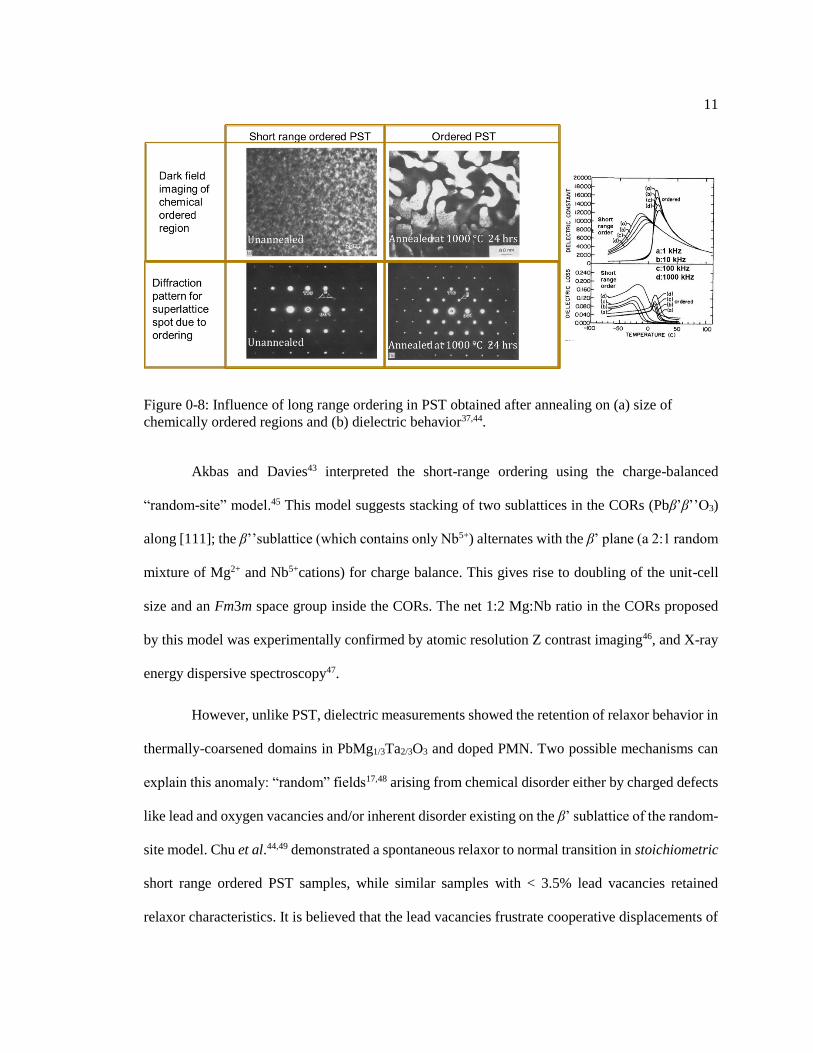
Figure 0-8: Influence of long range ordering in PST obtained after annealing on (a) size of
chemically ordered regions and (b) dielectric behavior37,44.
Akbas and Davies43 interpreted the short-range ordering using the charge-balanced
“random-site” model.45 This model suggests stacking of two sublattices in the CORs (Pbβ’β’’O3)
along [111]; the β’’sublattice (which contains only Nb5+) alternates with the β’ plane (a 2:1 random
mixture of Mg2+ and Nb5+cations) for charge balance. This gives rise to doubling of the unit-cell
size and an Fm3m space group inside the CORs. The net 1:2 Mg:Nb ratio in the CORs proposed
by this model was experimentally confirmed by atomic resolution Z contrast imaging46, and X-ray
energy dispersive spectroscopy47.
However, unlike PST, dielectric measurements showed the retention of relaxor behavior in
thermally-coarsened domains in PbMg1/3Ta2/3O3 and doped PMN. Two possible mechanisms can
explain this anomaly: “random” fields17,48 arising from chemical disorder either by charged defects
like lead and oxygen vacancies and/or inherent disorder existing on the β’ sublattice of the random-
site model. Chu et al.44,49 demonstrated a spontaneous relaxor to normal transition in stoichiometric
short range ordered PST samples, while similar samples with < 3.5% lead vacancies retained
relaxor characteristics. It is believed that the lead vacancies frustrate cooperative displacements of

12
the sublattices. Interestingly, the CORs in short range ordered-PST samples with lead vacancies (<
3.5%) were larger than those in stoichiometric samples. This work suggests the possibility that PbO
loss during long ordering anneals at 1473-1673 K in PbMg1/3Ta2/3O3 or doped PMN can promote
relaxor behavior, despite simultaneous coarsening of the CORs. Alternately, it can be hypothesized
that the relaxor characteristics can be correlated to the atomic disorder42 introduced by the random
distribution of the Mg2+ and Ta5+/Nb5+ ions on the β’ lattice in the CORs in PMT/PMN systems.
Chen et al.44,50 modelled the influence of the size of B-site cations (Mg vs. Nb) on the β’ sublattice
on strengthening the long range order – ferroelectric coupling. 1:1 order in adjacent sublattices was
reported to promote increased long-range coupling in the lattice, facilitating a relaxor-to-
ferroelectric transition due to increased displacement of the Pb2+ ion along the <111> towards the
β’ position42. This implies that relaxor behavior may persist even in stoichiometric Pb(B1/3B’2/3)O3
systems. There is a lack of experimental evidence to support the above assertion since fully-
ordered, stoichiometric PMN-type materials have not been grown as bulk ceramics, though varying
degrees of cation order have been achieved in a narrow window of kinetic activity and
thermodynamic stability.
In addition, the relation between the PNRs, CORs, and the freezing of the PNRs leading to
the non-ergodic phase in PMN is not clearly understood. At high temperature, the PNR clusters are
small and non-interacting; however, on cooling below TB, they can correlate with the neighboring
clusters and grow in size (as controlled by the correlation length). Drawing an analogy with spin
glasses, Viehland30,51 demonstrated that the frequency dependence of the dielectric data could be
fit with the Vogel-Fulcher relationship using a temperature-dependent correlation activation energy
among PNR clusters, followed by freezing at Tf given by the following relationship:
𝑓 = 𝑓0exp(𝐸𝑎
𝑘(𝑇𝑚−𝑇𝑓)) Equation 0-1

13
In Equation 0-2, Ea represents the activation energy for polarization fluctuations of an
isolated cluster. The temperature dependence of the equation can be attributed to the development
of short range order between neighboring clusters, with an interaction energy of kTf. The physical
model suggests that the polar clusters have a random distribution of polar orientations, similar to
the magnetization in spin glasses. When cooled, the polar clusters form a preferred polar
orientation, due to long-range interactions between the polar clusters. However, long-range
ordering is suppressed by the frustrated interactions during the freezing process, suggesting that
clusters could interact elastically through the rhombohedral distortion. The development of
correlation between these super-paraelectric moments leads to freezing at Tf, which is close to the
plateau temperature of correlation lengths, obtained via neutron scattering of PMN as shown in
Figure 0-9 5. A long-range ordered ferroelectric state can be achieved if these clusters percolate
(spontaneously44 or under an applied electric field28). Burton’s theoretical work using molecular
dynamics based on first principles52 in both PST and PMN proposed that the CORs act as
nucleation centers for the PNRs. Local fields due to chemical disorder in the paraelectric matrix
pin the PNRs from extending into the matrix, impeding the correlation between PNR clusters and
leading to the glassy state in PMN as shown in Figure 0-10. This could potentially imply that a
completely-ordered matrix with minor defects in PMN could suppress the formation of PNRs or,
at the very least, enable a spontaneous relaxor-to-normal-ferroelectric transition. Inelastic neutron
scattering techniques53 have demonstrated dampening of the transverse optic mode, a so-called
waterfall effect, when the material is cooled below Td. However, there is recovery of the TO
mode at temperatures around 213 K. Though this ordering is not visible via X-ray measurements,
nonlinear dielectric spectroscopy suggests a ferroelectric transition for field cooled PMN.

14
Figure 0-11: Temperature dependence of correlation lengths from neutron scattering of PMN at
Tf with insert showing fitting to Vogel Fulcher, indicating glassy behavior5.
Figure 0-12: Schematic showing nucleation, growth and interaction of polar nanoregions in COR
regions in a paraelectric matrix as a function of temperature.
Alternative microscopic models have been proposed to explain the key characteristics of
PMN. Originally proposed by Isupov, the breathing wall model by Glazounov and Tagantsev32,54
considers the polar cluster to be stabilized in orientation, but with interphase boundaries and
domain wall-like entities, that are responsive to temperature and electric fields. The observed
relaxor behavior of a single polar region is associated with the oscillation and movement of the

15
mobile walls due to an ac electric field, rather than thermally activated flips of local polarization.
This model is capable of describing the frequency dependence of the first and third harmonics of
PMN55. However, this model ignores the percolation of the interacting polar clusters through the
material. Westphal, Kleemann and Glinchuk17 proposed the “random field model”, suggesting
that the origin of the slowing down of the dynamics of PMN and its eventual freezing into non-
ergodic phase at low temperature is a result of quenched high temperature disorder inherent in
relaxor ferroelectrics with random orientations (electric dipoles, lattice defects, and
contamination). The model states the structural phase transition into a ferroelectric state is
destroyed by virtue of quenched random local fields. It is thought that the random fields and
random interactions between the defects and the polar regions leads to the freezing transition into
a glassy state, predicting the frequency dependence of the permittivity as a function of
temperature. This model also highlighted that the Barkhausen jumps observed during the poling
process (also observed by Colla56 et al.) do not agree with the glassy dipolar model on a
microscopic length scale.
To date, the origin and nature of non-ergodic behavior in relaxors remains controversial.
The commonly accepted model for PMN is the spherical random-bond–random-field (SRBRF)
model, which explains the low temperature freezing behavior by assuming that the formation and
freezing of polar nanoregions are distinct phenomena. In the spherical random-bond–random-
field (SRBRF) models57,58, Pirc and Blinc assumed that PNRs are spherical and interact randomly
via spin-glass type random exchange coupling, while being subjected to a random quenched
internal electric field (a frozen dipole glass state for relaxor). This model describes the
temperature dependence of the Edwards-Anderson glass order parameter q in terms of random
fields and random bonds. In the absence of random fields for certain limiting interacting bond
lengths, the theory predicts the transition from ergodic to ferroelectric phase with spontaneous

16
polarization. With increasing bond lengths, the system transforms into a spherical glass phase
without long range order. The presence of random fields destroys the phase transition with non-
zero q.
Relaxor to normal ferroelectric transitions can be introduced to PMN with addition of B-
site substitutional as shown in Figure 0-13 59–62. For example, addition of >10 vol. % Ti to PMN
stabilizes the rhombohedral phase with polarization along <111> upon cooling61. Interestingly,
increasing Ti concentration can increase the size of the polar macrodomain, but also causes
dilution of the electrostatic and strain interactions between Nb5+ and Mg2+ ions, thus reducing
their tendency to order.63 This makes 67PMN-33PT (morphotropic phase transition composition)
a disordered perovskite.
Figure 0-14:(a) Temperature dependence of the dielectric permittivity of PMN ceramic with
increasing PT as a function of frequency. (b)Temperature dependence of the reciprocal of
dielectric permittivity for PMN ceramic with increasing PT (<36%), where the straight lines
reveal that the dielectric responses of PMN-PT ceramics start to follow Curie–Weiss law at the
temperature much higher than Tmax for PMN.
2.2 Rayleigh analysis: probing nonlinearity in normal ferroelectric and relaxor ferroelectric
thin films
Small signal dielectric nonlinearities can provide insight into the response of mobile
interfaces like domain walls64–67, phase boundaries or nano-polar regions68–71 to dynamic electric

17
fields, in addition to intrinsic lattice responses. This can be a valuable tool in understanding the
contributions of mobile interfaces in both normal ferroelectrics and materials along the
ferroelectric-relaxor continuum. The Rayleigh law was first used by Neel et al.72–74 to describe the
physical origin of magnetization induced in a ferromagnetic material, due to the displacement of a
single ferromagnetic domain wall in an environment in which the potential energy of the wall
varies irregularly with position of the wall. He proposed that the randomly distributed pinning
defects in a material introduce perturbations in the potential energy for domain wall motion; the
resulting domain wall displacement produced Rayleigh characteristics (reversible linear and
irreversible quadratic component as shown in Figure 0-15) The law is valid for low-field
conditions, where the density and the structure of the domain walls remain unchanged, as the
field is cycled. The hysteretic behavior arises when the walls moves from one potential minima to
another, corresponding to the pinning and depinning of the domain walls by pinning centers.
Figure 0-16: Potential energy landscape for domain wall motion in an environment with
randomly distributed pinning centers75
Drawing an analogy with ferromagnetic materials, the Rayleigh law has been applied to
describe the nonlinear dielectric and piezoelectric response in ferroelectrics73,76. For example, the

18
dielectric permittivity or piezoelectric coefficient as a function of amplitude of ac electric field
Eac, has a reversible component, εinit or dinit, and an irreversible component, αe or αd, as described
in Equations 0-3 and 0-4.
𝜀 = 𝜀𝑖𝑛𝑖𝑡 + α𝑒E𝐴𝐶 Equation 0-5
𝑑 = 𝑑𝑖𝑛𝑖𝑡 + α𝑑E𝐴𝐶 Equation 0-6
The initial permittivity and piezoelectric constant are attributed to the intrinsic lattice
response and the non-lossy reversible movement of domain walls and phase boundaries. The
irreversible domain wall or phase boundary motion and its dependence on the external ac field
occur when the applied field is sufficiently large to overcome the potential barrier separating local
energy minima. The Rayleigh law only applies in the regime where the permittivity and
piezoelectric constant scale linearly with the ac electric field. Typically, this range is up to ⅓ – ½
the coercive field. For a Rayleigh-like ferroelectric material, the link between non-linearity and
hysteresis also describe the sub-switching polarization response65,77, as shown in Equation 0-4,
where P is the polarization, E = E0 sin ωt is the applied alternating electric field, 𝜀𝑖𝑛𝑖𝑡 is the
dielectric permittivity at the zero field, and 𝛼 is the Rayleigh coefficient. The sign “+” stands for
decreasing and “-” for the increasing part of the alternating field.
𝑃 = (𝜀𝑖𝑛𝑖𝑡 + 𝛼𝐸0)𝐸 ± 𝛼(𝐸2 − 𝐸02) + ⋯ Equation 0-4
It is important to note that for a more complete description of a real, non-ideal material,
Equation 0-4 may possess additional terms reflecting the degree of randomness of the energy
profile74. Investigation of an ac-signal through its harmonic amplitudes and phase angles is useful
to study nonlinear systems. Harmonic analysis of the sample response permits the study of
different contributions to nonlinearity, if the material response is the result of several
contributions differently depending on time.

19
2.3 Role of substrate clamping in thin ferroelectric films
The dielectric and piezoelectric responses of a ferroelectric material arise from contributions
of both the intrinsic lattice (controlled by the material structure and composition) and extrinsic
factors like domain wall mobility and motion of phase boundaries (which will be influenced by
stoichiometry, mechanical boundary conditions and defect concentrations)72. The extrinsic
contributions to the piezoelectric response are due primarily to non 180° domain walls, though
nearly reversible motion of purely ferroelectric walls can also contribute67. Extrinsic responses in
ferroelectrics can be pinned by point and line defects, grain boundaries and the substrate (for films)
among other factors 66. Lateral and thickness scaling of these films is required for various
applications, and necessitates improved understanding and quantification of the factors influencing
the piezoelectric response in thin films such as (i) grain size and orientation78–81, (ii) property
degradation owing to process- induced damages82–86 and (iii) elastic interaction at the film-substrate
interfaces.87,88
Among these factors, substrate-induced clamping can significantly reduce the converse
piezoresponse coefficient d33,f in continuous piezoelectric films, relative to single crystal values for
the same composition89–95. Application of the electric field to the thin ferroelectric film induces an
out-of-plane piezoelectric strain. However, as the film expands out-of-plane, it contracts in-plane
due to the d31 coefficient. Because the film is bonded to the underlying substrate, the lateral
contraction is frustrated, thereby reducing the out-of-plane strain. Assuming zero in-plane strain in
the thin film, this effective d33,f can be calculated using the formulation proposed by Lefki and
Dorman given as:
𝑑33,𝑓 = 𝑑33−2𝑑31𝑠13
𝐸
𝑠11𝐸 +𝑠12
𝐸 Equation 0-7

20
where 𝑑33is the unclamped piezoelectric coefficient of the film, 𝑠𝑖𝑗𝐸 are the mechanical
compliances at constant strain and 𝑑31 is the transverse piezoelectric coefficient.
Lateral patterning can reduce the residual stress state of the film, affecting the intrinsic
response and lowering the energy barriers for domain wall motion. Nagarajan89 et al.
demonstrated a ~3x increase in d33,f from switching ferroelastic 90° domain walls (from the in-
plane a-domain state to a c-domain state) in partially declamped micron sized islands ion-milled
in 100 nm thick epitaxial PbZr0.2Ti0.8O3 films. Additionally Griggio94 et al. and Wallace95 et al.
have shown that the 90° ferroelastic domain reorientation in released PbZr1-xTixO3 films is
comparable to that in bulk ceramics of similar composition. Keech92 et al. demonstrated that
subdividing a 350 nm thick 0.7PbMg0.33Nb0.67O3-0.3PbTiO3 film (grown on platinized silicon)
into 300 nm wide lines produces a ~3x enhancement in dielectric response and a 300% increase
in irreversible domain wall contributions; the effect of substrate release exceeded that of etch-
induced damage. Such declamping will have a profound impact on several applications - one such
example is the high speed, low power piezoelectric transistor10 proposed by IBM to address the
challenges posed by stalled clock speeds in complementary metal oxide semiconductor transistor
(CMOS) technology9. This approach relies on the high strain generated in nanostructured
piezoelectric films to actuate a piezo-resistive switch element. There is, therefore, a growing need
to develop high accuracy and high-resolution metrology for characterization of patterned
piezoelectric thin films.

Chapter 3
Relaxor behavior in ordered lead magnesium niobate (PbMg1/3Nb2/3O3) thin
films
Portions of this chapter are reproduced from: Smitha Shetty, Anoop Damodaran, Ke Wang,
Yakun Yua1, Venkat Gopalan, Lane Martin and Susan Trolier-McKinstr1, “Relaxor Behavior in
Ordered Lead Magnesium Niobate (PbMg1/3Nb2/3O3) Thin Films,” Advanced Functional
Materials 118, 174104 (2018).
3.1 Introduction
Fully-ordered, stoichiometric PMN materials have not been grown as bulk ceramics,
though varying degrees of cation order have been achieved with doping in a narrow window of
kinetic activity and thermodynamic stability7,42. In bulk materials, the chemically ordered regions,
formed at or below the sintering temperature (~1223K), are limited to 2-5 nm in dimension.
PMN undergoes a thermodynamic order-to-disorder transition at temperatures below
1073 K, which might kinetically restrict the development of ordered phase7,41,42. This work aims
to address this kinetic-growth limitation required to achieve a thermodynamically-stable, ordered
state in PMN, via synthesis of thin PMN heterostructure films with ordered layers of
stoichiometric Pb[Mg2/3Nb1/3]O3 and PbNbO3 grown at lower temperature as per the charge
balanced random site model. This is illustrated in the schematic in Figure 3-1. (111)-oriented
films were grown on SrTiO3 substrates with conducting La0.7Sr0.3MnO3 bottom electrodes using
timed pulsed-laser deposition. Without RHEED, it was not possible to get layer-by-layer growth
in these relaxed films. That said, for any area on the surface, the fluxes were delivered with

22
alternating compositions. This enabled growth of local long range ordered
Pb([Mg2+2/3Nb5+
1/3]1/2[Nb5+ ]1/2)O3 regions in the film matrix with reduced relaxor-like behavior at
length scales not achievable in bulk, while ensuring local lead stoichiometry. Though the relaxor
behavior did not switch “off”, this work can have implications on understanding the impact of
chemical ordering on polar domains in PMN. TEM characterization, supported by dielectric and
second-harmonic generation measurements, suggests that the low-temperature state of these PMN
heterostructures is ferroelectric with domains of tens of nanometer size, similar to the assertion
made by Fu et al. in PMN single crystals96. With decreasing temperature, it is speculated that
there is a continuum of ferroelectric and relaxor behavior, with increased percolating volume
fraction of PNR in long range ordered PMN heterostructure films.
Figure 3-1: Proposed PMN heterostructure with alternate PbNbO3 and PbMg
2/3Nb
1/3O
3 layering
along <111>
3.2 Experimental procedure
Prior to deposition, (001) and (111) SrTiO3 substrates were prepared by chemical etching
with a 50:1 buffered-oxide etchant (BHF) for 6 minutes, followed by a thermal anneal at 1273 K
for 3 hours in order to achieve step-terrace structures for the step-flow/layer-by-layer growth of the

23
bottom electrode. La0.7Sr0.3MnO3 films (~45 nm thick) were epitaxially grown as the bottom
electrode on the treated SrTiO3 substrates by pulsed-laser deposition, employing a KrF excimer
laser (248 nm; Coherent LPX305) from a ceramic La0.7Sr0.3MnO3 target (Praxair Specialty
Ceramics). The La0.7Sr0.3MnO3 layer was deposited at 973 K in an oxygen pressure of 100 mTorr,
with a laser fluence of 1.5 J/cm2 at a repetition rate of 5 Hz. Heterogeneous long-range-ordered
PMN film growth was achieved via subsequent pulsing of the Pb1.2NbO3.2 and Pb1.2Mg2/3Nb1/3O3.2
targets doped with 1% La doped at 873 K in an oxygen pressure of 200 mTorr at a laser fluence
of 0.75 J/cm2 and a laser repetition rate of 3 Hz. Short-range-ordered PbMg1/3Nb2/3O3 films were
also grown from a single stoichiometric PMN target with 20% excess Pb, under similar growth
conditions for comparison. Following growth, all samples were cooled to room temperature at a
static oxygen pressure of 100 Torr. For clarity, the multi-target films are referred as long-range-
ordered PMN heterostructures (LRO) while the single target films are referred as short-range-
ordered PMN (SRO). Additionally, initial heterostructure growth results using RHEED based
pulsed laser deposition system have been summarized in Appendix A.
The crystalline structure of the films was investigated by PANalytical 4-circle X’Pert 3 MRD
X-ray diffractometer (XRD) with Cu Ka radiation (PANalytical B.V., Almelo, The Netherlands).
Compositional analysis was performed on the two-target films using Rutherford Backscattering by
Liv Dedon at the Lawrence Berkeley National Laboratory with incident ion energy of 3040 keV,
incident angle α (22.5 °), exit angle β (25.35 °), and scattering angle (168 °). Data were fit using
the SIMNRA software ( Max-Planck-Institute for Plasmaphysics, Germany). 100-nm-
thick platinum top electrodes were sputter deposited via a lift-off procedure for electrical
characterization. Temperature-dependent structural characterization was achieved using a Gatan
cooling in-situ holder (Model 613) on a Titan3 dual aberration corrected scanning/TEM (S/TEM)
operated at 200 kV. Room temperature selected area electron diffraction followed by dark-field
imaging was used to identify the F-type ordering spot {h+1/2, k+1/2, l+1/2} and chemically-

24
ordered domains for both long range ordered and short range ordered PMN samples, similar to the
procedure employed in bulk samples63. In addition, the PNRs were imaged at the 111-fundamental
reflection as a function of temperature (100-296 K) in the long range ordered PMN heterostructures.
TEM specimens were prepared by in situ milling in a FEI Helios NanoLab DualBeam 660 focused-
ion beam (FIB). Before milling, a thick protective amorphous carbon layer was deposited over the
region of interest by electron-beam deposition. The FIB-TEM membrane was fabricated with a
starting milling voltage of 30 kV that was then stepped down to 2 kV to minimize sidewall damage
and thin the specimen to electron transparency.
Temperature dependent polarization – electric field hysteresis loops, small signal dielectric
response, and the ac field dependence of the dielectric response were characterized using a cryo-
cooled probe station (Lakeshore CRX-VF) from 10 -350 K. Prior to measurement, both long-range-
ordered and short-range-ordered samples were annealed at 723 K in a rapid thermal annealer for 1
min to erase any aging. The samples were subsequently zero field cooled to 10 K in the cryocooled
probe station and the dielectric response was measured on heating. Polarization-electric field (P-E)
hysteresis loops were measured at 10 kHz using a Multiferroic tester (Radiant Technology, Inc.
Albuquerque, NM). The ac field and frequency dependence of the relative dielectric permittivity
was characterized using an HP 4248A precision LCR meter (Agilent Technology, Palo Alto, CA)
from 0.5-100 kHz. Thermal depolarization measurement was carried out on long-range-ordered
PMN heterostructure film using a pA meter (HP 4140 B) during zero-field heating (heating rate of
~4 K/min) in the temperature range of 75-400 K. The sample has been previously cooled under an
electric field of 200 kV/cm (cooling rate of ~1 K/min). Second harmonic generation measurements
were conducted to verify the transition temperature and symmetry breaking without the application
of an electric field. A Janis ST300 (Janis Research Company, Woburn, MA) temperature system
with liquid nitrogen coolant was used to control the sample temperature during measurements. The
samples were probed using a Solstice Ace (Spectra-Physics, Santa Clara, CA) femtosecond pulsed

25
laser beam (100 fs, 1kHz) at a fundamental wavelength of 800 nm. The second harmonic signal
(400 nm) was detected using a photomultiplier tube (Hamamatsu H7826, Hamamatsu, Japan) and
a Stanford Research (Sunnyvale, CA) SR830 lock-in amplifier.
3.3 Results and discussion
3.3.1 Structural/compositional characterization
XRD patterns for the long-range ordered PMN heterostructure and the short-range-ordered
PMN films, grown on (001) and (111) STO substrates are shown in Figure 3-2(a). Phase pure
perovskite films were obtained for growth on (111) substrates, while a niobium-rich second phase
developed for films on (001) STO. Long-range-ordered PMN heterostructure films exhibited a full
width half maximum of 0.1º in the ω rocking curves about the 111 reflection, as shown in the inset
of Figure 3-2(b). Superstructure reflections of type (1/2 1/2 1/2) were not observed in the XRD
pattern. This could be attributed to the incomplete ordering and/or length scale of the randomly
distributed chemically ordered regions. Single target short-range-ordered PMN films were also
found to be phase pure. PMN is relaxed at the grown thicknesses for both short-range and long-
range films. Compositional analysis using the Rutherford backscattering technique, as shown in
Figure 3-3 (a) and (b) shows the average film composition in a long-range-ordered film. Note the
Mg peak was very close to the noise level and can skew the Mg:Nb ratio fit.

26
Figure 3-2: (a) XRD pattern for long range ordered PMN heterostructure film grown on 001 and
111 STO (labelled as PMNLRO)and short range ordered PMN on 111 STO (labelled as PMNSRO)
(b) ω-scan for 111 reflection on 30 nm PMN heterostructure film grown on STO.
Figure 3-3: (a) Simulated data fit to the experimental data on the long range ordered PMN
heterostructure film obtained by Rutherfold Backscattering (b) Calculated elemental composition
from simulation.
ω/°
Intensity/a
rbitra
ry (a) (b)
Intensity/a
rbitra
ry

27
A TEM image [Figure 3-4(a)] and the fast Fourier transform (FFT) from the corresponding
high resolution TEM image from the same region (Figure 3-4(b)) indicate epitaxial growth of the
100 nm thick PMN heterostructure on the 45 nm thick LSMO bottom electrode. No evidence of
secondary phases was observed in the sample by TEM, in agreement with the XRD
investigations. The dislocation density is not so high, though there are some edge dislocations at
the interface; these dislocations are somewhat curved and appear without a fixed period. The FFT
along the [-112] pole shows the (½, ½, ½) superstructure reflections indicating cation ordering.
The dark field images in Figures 3-4(c) (d) and (e) were acquired using one of these
superstructure reflections and show long-range-ordered domains as large as 150 nm (marked as a
dotted region in the image (d). Fig 3-4(c), (d) and (e) shows the chemically ordered regions are
distributed in the heterostructure film (throughout the TEM sample size). Figure 3-5 (a) is a TEM
image showing the cross-sectional structure of a short-range-ordered PMN film on LSMO/STO.
In contrast, the FFT from the corresponding high resolution TEM image of the epitaxial PMN
deposited from the single target shows diffuse superlattice reflections for chemical ordering, as
expected. Additionally, in the dark field TEM data (Figure 3-5(c)), fewer ordered regions were
observed with sizes less than 10 nm.
(b)

28
Figure 3-4: (a) A cross-section TEM image of a long range ordered heterostructure PMN (111)
film (marked LRO-PMN) on LSMO/STO (111) recorded along the [−112] pole (b) FFT from a
high resolution TEM image showing superstructure reflections; (c)(d) (e) cross-sectional dark
field images captured using one of the superstructure reflections in (b), revealing the highlighted
cation-ordered domain in the film.

29
Figure 3-5:(a) A cross-section TEM image pattern of a short range ordered PMN (111) film
(marked SRO-PMN) on LSMO/STO (111) (b) FFT of a high resolution TEM image recorded
along the [−112] pole showing diffused superstructure reflections (marked by blue circles)
associated with short-range cation ordering; (c) a cross-sectional dark field image captured using
one of the superstructure reflections in (inset), revealing cation-ordered domains in the PMN film
of a few tens of nm in size.
Figure 3-6 show the bright and dark field images of the same area imaged using the 111
reflection at room temperature and 100 K in situ, obtained during a heating cycle for the long-
range-ordered PMN heterostructure. Figure 3-6(a) and (b) were collected at room temperature,
while (c) and (d) were at 100 K. Clearly the microstructures are very different between these two
temperatures. In the dark field images (Figure 3-6(d) and (e)) shown at 100 K, a fringe-like
contrast having a spacing of ~0.7 nm is seen in volumes with columnar shape. The long axis of
those columnar regions is normal to the interface; the domains are ~10-20 nm in size along the
short axis and ~50 nm along the long axis. This observation is consistent with the polar
microdomain imaging in the (110) orientation, reported in bulk PMN during heating59,97. These
fine structures disappear as the film is heated beyond 220 K, as evident in the temperature
dependent nanopolar imaging shown in Figure 3.7. These fringe-like structures are speculated to
be a result of polar macrodomains of the rhombohedral phase, as suggested by previous work59,97.

30
The average fringe distance (D) was measured to be approximately 0.7 nm, which is unlikely to
be Moire fringes caused by lateral overlapping of 111 planes (d spacing= 0.225 nm).
Additionally, a rotational Moire pattern is assumed to exist, the twist angle (α)98 calculated using
the relation (D=d/2 sin (0.5 α)) turns out to be 18°, which is inconsistent with epitaxy. In addition,
these features are consistently temperature dependent. Based on the contrast from dark field, the
volume fraction of the polar cluster was estimated to be ~20-30% at 100K. This volume fraction
is above the theoretical prediction for geometrical in-plane percolation threshold99 (18-20%) for
iso-parametric overlapping ellipsoidal clusters with aspect ratio ranging from 1:5 to 1:2.5 and
consistent with the neutron scattering pair distribution function analysis results at 15K by Jeong et
al.100. This favors the prevalence of ferroelectric state in ordered PMN at low temperature.
Figure 3-6: (a),(b) Cross-sectional bright and dark field TEM image of ordered heterostructure
PMN (111) film on LSMO/STO (111) at 296 K (c),(d) A cross-section bright and dark field TEM
image of or PMN (111) film on LSMO/STO (111) at 10 K, (e) A magnified dark field image (red
circular regions show polar fringes) and (f) magnified image showing evidence of polar
nanoregion striations through the film thickness with interfringe spacing of ~7 nm.

31
Figure 3-7: Temperature evolution of the polar nanoregion from 100 -220K. The polar
nanoregion fringe like structures disappear completely at 220 K.

32
3.3.2 Electrical characterization
The ferroelectric properties of the ordered PMN heterostructure film were studied by
polarization – electric field (P-E) hysteresis loop measurements as a function of temperature. Slim,
but well-defined nested hysteresis loops were obtained, as shown in Figure 3-8a, with low levels
of leakage. At room temperature, twice the remanent polarization (2Pr) and coercive field (Ec) of
the heterostructure PMN film were found to be 11.3 ± 0.3 μC/cm2 and -110 kV/cm, respectively.
Compared to short range ordered films, the polarization increased by 38% under similar electric
field conditions. The polarization value is considerably higher than in previously reported work,
presumably due to stabilization of the field-induced polarization as a consequence of the partial
cation ordering achieved in the film. The ferroelectric behavior of the films was also confirmed by
capacitance-field measurements; as shown in Figure 3-8b, the data show switching peaks that are
the fingerprint of the ferroelectric switching. Increasing nonlinearity and hysteresis was observed
in large signal P-E hysteresis loops as the temperature was lowered to 10 K. At low temperature,
the loops became increasingly square [Figure3- 8(c)]; on heating. the temperature dependence of
the remanent polarization reveals a gradual loss in polarization with temperature which is consistent
with relaxor characteristics. As shown in Figure 3.8 (d), compared with measured and calculated
√Ps2 in bulk ceramic and single crystal PMN14,15, the observed polarization is lower, however
confirms a decreasing trend up to TBurns (~600 K).
Figure 3-9(a) and 3-9(b) show the temperature dependence of the relative dielectric constant
and its loss at different frequencies, for 100 nm thick long-range-ordered and short-range-ordered
PMN films. The long-range-ordered PMN heterostructure shows less dispersion of the permittivity,
compared to that found in the short-range-ordered film. The shift in Tmax (compared at the highest
and the lowest frequencies) in the case of a short-range-ordered film is ~40 K, however in the case
of long-range-ordered film, this difference is ~25 K. In the long-range-ordered film beyond Tmax,

33
the dielectric response converged while more space charge in the short- range-ordered film leads
to a failure to converge the permittivity data above Tmax. As expected, the maximum permittivity
of the PMN thin film is much below that of bulk ceramics (~16,000), which is certainly due, at
least in part to substrate clamping79,101.
Figure 3-8:(a) Room temperature P-E loop evolution as a function of ac field; (b) permittivity
field data at 10 kHz showing switching (c) Twice the remanent polarization (2Pr) as a function of
temperature with an inset showing polarization evolution in long-range-ordered PMN

34
heterostructure thin films at select temperatures (d) Comparison of LRO polarization as a
function of temperature upto TBurns (~600 K) with bulk ceramic and single crystal PMN.
Figure 3.9: (a) Temperature dependence of dielectric response for long-range-ordered PMN films
as a function of frequency measured during a heating cycle (b) Temperature dependence of
dielectric response for short-range-ordered PMN films as a function of frequency during a heating
cycle. Note: arrows indicate increasing frequency (from ~ 1 kHz - ~ 300 kHz). In both cases, the
upper set of curves correspond to the permittivity and the lower set of curves correspond to the
loss tangent.

35
The relaxor behavior did not turn “off” completely in the long-range-ordered sample, despite
observing increased size of chemically ordered regions in TEM. Electron diffraction is poor at
distinguishing complete and partial ordering. Recent atomic resolution HAADF STEM imaging
work by Lebeau et al.102 demonstrated the presence of chemical order gradients within each COR
in relaxor PMN, rather than abrupt transition between the COR and disordered matrix, as shown in
Figure 3.10 (a). Also, the order metric (defined as the standard deviation of the Mg/Nb atom column
intensities surrounding each Pb/O atom column normalized to mean) is independent of the COR
size in the ordering gradient mode as shown in Figure 3.10 (b). Thus, relaxor behavior in PMN
might be strongly influenced by the disorder inherent in the β’ sublattice of the COR in the ordered
PMN films. This random positional disorder cannot be controlled during growth and
hence ordering along one dimension is not enough to turn off relaxor ferroelectricity. Our results
assert a mixture of ferroelectric and relaxor behavior in the long-range-ordered PMN
heterostructure films, as the ordering observed is inadequate to drive a fully ferroelectric state.
Figure 3.10: (a) Order metrics match for a 4 nm representative COR from experiment with ordering

36
gradient model proposed by LeBeau et al.102 (b) Average order metrics as a function of COR size
Figure 3-11(a) shows the effect of increasing ac field (3-25 kV/cm) as measured at 1 kHz on
long-range-ordered PMN films, as a function of temperature. The permittivity increased linearly as
a function of ac field, with Tmax shifting to lower temperature. These data were fitted using the
Rayleigh law 𝜀𝑟 = 𝜀𝑖𝑛𝑖𝑡 + 𝛼𝐸𝑎𝑐 for ac fiels up to ~1/3-1/2*coercive field. The irreversible
Rayleigh coefficient α represents the irreversible movement of domain walls, polar cluster
boundaries, or phase boundaries, while εinit arises from both the intrinsic response and reversible
motion of boundaries. The Rayleigh coefficients decrease at higher frequencies, which would be
consistent with observations by Glazunov et al.103 in PMN single crystals. These data suggest a
domain wall or interface boundary type relaxation phenomenon, instead of the thermally activated
polarization flips, as would have been suggested by the superparaelectric model. As observed in
Figure 3-11(b), α peaked at 130-140 K for the heterostructure sample. The decrease in α at low
temperatures is presumed to be due to loss of thermal activation of the mobile boundaries, as
described by Li et al.5 The decrease in α at high temperature is likely to be due to a reduction in
the number of mobile boundaries; this could be due to loss of a long-range-ordered ferroelectric
phase or to a decrease in the volume fraction of micropolar regions. For the short-range-ordered
PMN film, α goes through a similar peak, but the magnitude of α is smaller.
Figure 3-12 shows the thermal depolarization current density measured on heating under zero
field conditions in the long range ordered PMN heterostructure films from 75 K-275 K. This shows
the presence of depolarization temperature peak at ~125 K, which is in close agreement to the
maximum in the irreversible Rayleigh coefficient. This peak would correspond to the discharge of
the polarization developed during the prior field cooling on the sample, similar to field induced

37
normal ferroelectric to relaxor phase transition in doped PMN ceramics104. The calculated
polarization, obtained by integrating the area under the curve in the temperature range from 75 K-
225 K was ~4.2 μC/cm2. This low value may be attributed to the loss in polarization due to time
dependent zero field aging, previously observed in PMN single crystals above 200 K105,106. The
depolarization temperature at 125 K is much lower than that in undoped bulk PMN (~213 K), which
may be partly attributed to 1% La doping of the Pb1.2Mg2/3Nb1/3O3.2 target; as demonstrated by Zhao
et al104.
Figure 3-11: (a) Dielectric permittivity of ordered PMN as a function of ac field measured at
1kHz (b) Reversible and irreversible Rayleigh coefficients of the relative permittivity of a
heterostructure PMN film as a function of temperature (c) Reversible and irreversible Rayleigh

38
coefficients of the relative permittivity of a short-range-ordered PMN film as a function of
temperature
Figure 3-12: Depolarization current from long-range-ordered PMN on heating at E=0 KV/cm,
after cooling at E=275 kV/cm, showing peak at 125 K. Data measured for the other polarization
direction were extremely noisy due to low retention of the poled state.
3.3.3 Second harmonic generation (SHG) optical measurement
Second harmonic generation measurements were used to further investigate the
heterostructure films as a function of temperature. This technique does not require the application
of electric fields, eliminating the potential impact of the small signals used for dielectric
characterization on nucleation of a long-range-ordered ferroelectric phase. Figure 3-13 shows the
SHG response for LSMO (bottom electrode), short-range-ordered PMN film and the long-range-
ordered PMN heterostructures during heating and cooling cycles. Compared to short-range-

39
ordered PMN, the long-range-ordered PMN films showed larger signals, suggesting an increased
volume of a polar phase or larger nonlinear optical constant. Additionally, in the case of the PMN
heterostructures, onset of features were consistently observed in the SHG data at 130 K during the
heating cycle; the 130 K anomaly matches the temperature of the peak in the irreversible
Rayleigh coefficient. This might indicate a change in ferroelectric ordering, due to the disruption
of percolated domains (formed during the cooling cycle) with increasing temperature.
Figure 3-13: Second harmonic generation results for LSMO on STO substrate, short-range-
ordered PMN and long-range-ordered PMN heterostructure during heating and cooling cycles
The difference between the short-range and the long-range-ordered PMN films, shown by
the second harmonic and electrical characterization might imply a difference in the percolation of
polar microdomains, with increased ferroelectricity in the ordered case. This work shows that the
degree of relaxor character in thin film PMN can be reduced with increased length scales for the
cation ordering (e.g. when the size of the chemically ordered regions approaches 100 nm) via
engineered growth of heterostructures with alternate layers of Pb(Mg2/3Nb1/3)O3 and PbNbO3.

40
These heterostructures possess some characteristics of relaxor and some of normal ferroelectric
behavior. Ferroelectric domains develop in the long-range-ordered films below 140K under zero
field cooling conditions. Results on growth and electrical characterization of PMN
heterostructures on scandate substrates have been discussed in Appendix B. Similar trends in the
temperature dependent dielectric behavior of PMN heterostructure (as a function of ac field and
frequency) were observed on the scandate substrates as STO. This indicates substrate does not
influence the observed properties in the long-range ordered films.

Chapter 4
Non-linearity in engineered lead magnesium niobate (PbMg1/3Nb2/3O3) thin
films
4.1 Introduction to non-linear susceptibility in relaxor ferroelectricity
Small signal dielectric nonlinearities can be used to probe the response of domain walls64–67 or
nanopolar regions68–71 to oscillating electric fields. This can be a valuable tool in understanding
the ferroelectric-relaxor continuum model observed in long range ordered PMN films. In
materials containing ferroelectric domain walls with a randomly broad and uniform distribution
of pinning centers, the polarization response in the sub-switching regime (E<~1/2 Ec ; where Ec:
coercive field) may be approximated by the Rayleigh relation74:
𝑃 = (𝜀𝑖𝑛𝑖𝑡 + 𝛼𝐸0)𝐸 ± 𝛼(𝐸2 − 𝐸02) + ⋯. (Equation 4- 1)
where P is the polarization, E = E0 sin ωt is the applied alternating electric field, 𝜀𝑖𝑛𝑖𝑡is the
dielectric permittivity at zero field, and 𝛼 is the irreversible Rayleigh coefficient; the “+” sign
corresponds to decreasing and “-” to increasing field. The above relationship can be expanded
into a Fourier series64 as:
𝑃 = (𝜀𝑖𝑛𝑖𝑡 + 𝛼𝐸0)𝐸0 sin𝜔𝑡 −4𝛼𝐸0
2
3𝜋cos𝜔𝑡 −
4𝛼𝐸02
3𝜋[1
15cos3𝜔𝑡 −
1
105cos 5𝜔𝑡 +⋯ . ]
(Equation 4-2)

42
The higher harmonic terms are 90 ° out-of-phase with the driving field; as a result, they
contribute both to the nonlinearity in the polarization and to hysteresis. This model provides a
good description of the response of a number of ferroelectrics67,77 with mobile domain walls or
boundaries of polar clusters. This field dependence of the phase angle of the higher order
harmonic permittivity has been used to investigate the presence of Rayleigh-like behavior in
Ba0.6Sr0.4TiO3 ceramics107, by Hashemizedah and Damjanovic. In those ceramics, the phase
angles were inconsistent with Equation 2. Instead, the behavior was consonant with harmonic
analysis of PMN ceramics above Tmax, where the polar entities provide a nonlinear, but nearly
anhysteretic response33 as a function of the electric field, implying that the Rayleigh-like analysis
cannot be used to fully explain the dielectric response in this regime.
The non-linear dielectric properties are also important in discriminating between existing
models for relaxor ferroelectrics, since it is believed that the higher order susceptibilities are more
sensitive to the dipolar disorder than the linear parameters70. In globally centrosymmetric materials
like PMN, the dielectric response between induced polarization (P) and the electric field (E) should
be given by the expression:
𝑃 = 𝜀0(𝜒1𝐸 + 𝜒3𝐸3 +⋯) (Equation 3)
where𝜒1 and 𝜒3 are the first and third harmonic susceptibilities. There are several conflicting
studies on the temperature dependence of the scaled susceptibility parameter a3 (defined as a3=
−𝜒3/𝜀03𝜒1
4) in the vicinity of the static freezing temperature (Tf) of relaxors. In principle, a3
should distinguish between models in which PMN transforms into a ferroelectric state with
nanodomains or diverges into a freezing transition, as in the case of dipolar glass68.
The most widely accepted model for PMN is the spherical random-bond–random-field
(SRBRF) model. In the SRBRF model, Pirc and Blinc assumed that spherical PNRs interact via
spin-glass type random exchange coupling, while being subjected to a random quenched internal

43
electric field.57,58. The model predicts a negative χ3 and a positive a3 with two extremes: one at
the freezing temperature Tf of the spherical glass phase and another at the Tmax. To date, this
prediction has been examined experimentally by a number of groups55,68,70 for PMN single
crystals. Bobnar et al.68 confirmed the theoretically predicted anomaly of a3 at Tf (a3 strongly
increases as the temperature approaches the freezing Tf~220 K, where ergodicity is effectively
broken for undoped PMN single crystal). Glazounov and Dec observed that a3 continues its
monotonic increase even below Tf, ≈ 220 K. A monotonic increase in a3 would be more in
agreement with the ferroelectric background picture of relaxors than with the glassy one. The
reported experimental data shows a positive sign of χ3, which can be explained either by
incorporating the effect of the electric field on the interacting polar clusters in the generalized
spherical random bond random field model108 or by including the average polarization of the
polar nanoregions in a modified Landau-Ginzburg-Devonshire formalism70. The signs and phase
of χ3 and the sign of a3 have been summarized in Table 4-1 for the Rayleigh model, the modified
phenomenological model for relaxors70 and the SRBRF model. It has been pointed out that many
of these seemingly contradictory observations could be due to the fact that the experimental
results were obtained in different regions of the electric field-temperature phase diagram5.
Namely, by cooling the relaxor at an electric field exceeding the critical field EC, a long-range
ferroelectric phase is formed. Thus, the field-history characteristic of the measurement can have a
profound effect on the results.

44
Table 4-1: Summary of signs for χ3 and a3 and phase for χ3 predicted by different relaxor models.
Sign of χ3 Phase of χ3 Sign of a3
Rayleigh model77,107 - -90 ° +
Modified LGD70
phenomenology-based model
for relaxors
+ NA -
SRBRF model57 - 180 ° +
Generalized SRBRF108 + 180° -
There are essentially two ways to characterize the third order non-linear dielectric response
𝜒3. The most reliable technique involves measurement of the polarization response at 3ω,
simultaneously with the linear response at ω at zero field dc bias. The second technique utilizes
the static electric field dependence of the linear dielectric constant, where 𝜒3 is defined as, 𝜒3=
[𝜒1(E2)- 𝜒1(E1)]/((E2)2-(E1)2]; this can be erroneous due to contributions from a phase transition
into a long-range-ordered ferroelectric state near Tf.
Although symmetry should forbid a second harmonic dielectric response in centrosymmetric
materials, measurable second harmonic contributions in the polarization response have been
reported for centrosymmetric phases of ferroelectric/relaxor crystals and ceramics like 60-40
BST107, PZN-PT109, BaTiO3109
, Sr0.61Ba0.39Nb2O6 etc. This has been attributed to the presence of
residual polarization that is the result of a previous application of an electric field and that has not
been completely removed by annealing the crystal at a temperature above Tmax due to presence of
micropolar regions or to a finite defect population, leading to local inhomogeneous fields and
quadratic dielectric displacement in the material. That is, a second harmonic can appear if the local
symmetry is non-centrosymmetric. Alternatively, a second harmonic can also be observed in cases

45
where mobile charges are trapped on the first cycle of the electric field110.
It is an open question as to how the level of cation ordering in a relaxor ferroelectric will
influence the higher order polarization terms as a function of temperature. In this work, the linear
complex dielectric susceptibility was analyzed as a function of temperature and frequency in zero
field cooled PMN films with short- and long-range ordering. Additionally, the second and third
harmonic displacement charge densities were determined as a function of temperature to assess the
influence of chemical ordering on the non-linear dielectric susceptibility. These, along with the
phase angles of the higher harmonics, were used to probe the ferroelectric-relaxor continuum
phenomenon observed in these films. In particular, of interest was which, if any of the models
shown in Table 4-1, described the behavior of these PMN films. The measurements made also
track the nonlinearity over a wider temperature range than has been reported previously.
4.2 Experimental procedure
For the second- and third order dielectric harmonics measurements, a sinusoidal ac oscillation
was applied using the built-in voltage source of a lock-in amplifier (Stanford Research Inc. SR-
830). A low-noise charge amplifier with a scaling factor of 1 V/100pC was used to amplify the
output signal of the sample. The charge amplifier showed very little change in amplitude (< 2 %)
and moderate phase errors (< 15 °) with a reference capacitor load similar to that of the PMN
films, at the highest measured frequency of ~60 kHz (e.g. the 3rd harmonic of the 20 kHz
fundamental). Over most of the frequency range, the phase angle was substantially smaller. The
resulting voltage from the charge amplifier was detected by the lock-in amplifier for the second
and third harmonics, sequentially. In this way, the magnitudes of the higher-order dielectric
charge displacement densities were measured as a function of temperature and frequency. The
harmonic displacement charge density is defined as Dn=Qn/A, where A is the area of the sample,

46
D is the induced displacement charge density, Q is the magnitude of the measured charge at the
desired frequency, and n is the harmonic order. Similar to the nonlinear dynamic approach
adopted by Hashemizadeh et al.107, the phase of the higher harmonic dielectric measurement was
measured to investigate the dynamics of the polar mobile interfaces (such as domains walls or
polar cluster boundaries), as well as to validate the Rayleigh-like behavior regime in the ordered
sample, as a function of temperature and ac field up to 100 kV/cm at 1 kHz.
4.3 Results and discussion
Figure 4-1 and 4-2 shows the temperature dependence of the real parts of the first (D1ω),
second (D2ω), and third (D3ω) harmonic dielectric displacement densities for short and long range
ordered PMN thin films, respectively, measured at 15 kV/cm. All three responses showed broad
frequency dependent maxima as a function of temperature in the frequency range from 0.5 to 20
kHz. D3ω is more frequency dependent than D1ω. As reported previously, the short range ordered
film shows a larger frequency dispersion in D1ω compared to the long range ordered film. This is
consistent with a higher degree of relaxor behavior in the short range ordered film. Interestingly,
the magnitude of D2ω is comparable to D3ω in both films and shows substantial frequency
dispersion above 200 K. The latter observation is likely to be due to increased conductivity at
higher temperatures, with a commensurate increase in trapping of mobile charges.110
The D3ω response has a complex shape with a change in sign, as a function of temperature and
frequency. There is a minimum in D3ω (i.e. the highest negative value) near the permittivity
maximum (observed at the highest frequencies), with the values converging back towards zero both
at 0K and well above Tmax. With increasing frequencies in both long and short-range ordered PMN
films, D3ω is more negative. The dispersion in D3ω is small at T<100 K, and increases in magnitude
with temperature, until it reaches 175 K in the case of long range ordered films and 200 K for short

47
range ordered film. On further heating, the frequency dispersion collapses. Persistence of dispersion
up to higher temperature in short range ordered film is consistent with a higher degree of relaxor
behavior.
Figure 4-2: (a) Temperature dependence of first order and third harmonic displacement current
for zero-field cooled long-range-ordered PMN films as a function of frequency (500 Hz-20 kHz)
measured on heating (b) Temperature dependence of second harmonic displacement current for
long-range-ordered PMN films as a function of frequency on heating. The dotted arrows indicate
increasing frequency (from 500 Hz -20 kHz). All measurements were done at an electrical field
of 15 kV/cm.
Figure 4-1: (a) Temperature dependence of first order and third harmonic displacement current for zero-
field cooled short-range-ordered PMN films as a function of frequency (500 Hz-20 kHz) measured on
heating (b) Temperature dependence of second harmonic displacement current for short-range-ordered PMN
films as a function of frequency measured on heating. The dotted arrows indicate increasing frequency
(from 500 Hz -20 kHz). All measurements were done at an electrical field of 15 kV/cm.

48
To develop additional insight into the mechanisms responsible for this behavior, the higher
harmonic polarization was measured as a function of temperature and the amplitude of ac electric
field for PMN films with cation ordering at different length scales. Figure 4-3 (a)-(d) illustrates the
phase of third harmonic contribution as a function of temperature. At low temperatures, after a
certain threshold electric field, the phase angle of the 1st harmonic is ~0°, while that of 3rd harmonic
is -90°, similar to that observed in PZT thin films77. This is consistent with Rayleigh-like hysteretic
responses of mobile interfaces like domain walls or polar cluster boundaries. The observation of
Rayleigh-like behavior at low temperatures is consistent with the drop in the magnitude of D3ω
below 100K, as the motion of domain walls (or cluster boundaries) is thermally activated. This
might also account for the relatively modest frequency dependence, with the largest response
occurring at the lowest frequencies.
At temperatures above ~180 K, the 3rd harmonic phase angle deviates towards 0 or -180°, as
shown in Figure 4-3 (c)-(e). The threshold field (defined as the minimum electric field for observing
Rayleigh response where the phase angle is close to 90°) was observed to decrease with increasing
temperature till 180K, with increasing Rayleigh-like behavior. This corroborates well with the peak
in the irreversible Rayleigh coefficient α at 150 K as reported elsewhere. At room temperature, the
3rd harmonic angle is close to -180°, representing an-hysteretic behavior similar to that reported in
bulk PMN. This means that the dielectric behavior at room temperature is governed by polar
nanoregions, whose dynamics cannot be explained using the Rayleigh law. This further supports
the continuum of ferroelectric and relaxor behavior with increasing temperatures. This may occur
as a result of increased relaxor behavior due to contributions for polar nano-region, as proposed by
the spherical random bond random field model.

49
Figure 4-3: Phase angle for the 1st and the 3rd harmonics of the polarization at 10K (a)-(d)
Hysteretic to anhysteretic transition in long-range-ordered PMN as demonstrated by 3rd harmonic
phase with increasing temperatures at 125 K, 180 K and 296 K respectively.
Figure 4-4 (a)-(e) shows the ac field dependence of the first (χ1), second (χ2), third order
susceptibilities (χ3) and scaled parameter a3 as a function of temperature, measured at 1 kHz for
the long-range-ordered PMN thin films. The linear susceptibility displays a broad maximum as a
function of temperature. The non-zero second harmonic observed in Fig 4-4(b) is largest below
150 – 170 K, consistent with previous observations of long-range ferroelectric ordering at these
temperatures12. The magnitude of χ2 remains non-zero, but decreases above this temperature,
consistent with the possibility of local polarization in the unpoled heterostructure above 170 K. In
this work, the difference in the maximum/minimum temperatures for χ1 and χ3 is larger than that
reported by Dec.70
As shown in Figure 4-4(c), at the lowest measured field (which is below the threshold field at
low temperatures, but well in the Rayleigh regime above ~120K), χ3 is mostly negative, with a
change in sign at temperatures above 200 K. At this field, the temperature where χ3 has its largest

50
negative magnitude corresponds well with the temperature at which the irreversible Rayleigh
coefficient has its maximum value, as reported elsewhere12. The change in sign shifts towards
lower temperatures with increasing ac field. The fact that χ3 is more positive at high AC electric
fields implies that domain wall contributions cannot be responsible for the sign change, as
Rayleigh contributions should produce a negative χ3. The positive χ3 is consistent with prior
reports by Dec for PMN ceramics. A transition from a non-hysteretic to hysteretic behavior is
seen with lowering temperatures. This suggests that the nonlinear properties must lie somewhere
on a continuum between normal and relaxor-like ferroelectrics.
A similar trend with ac field is also reflected in the scaled parameter a3, as seen in Figure 4-
4(d). Over most of the observed temperature range, a3 is small and negative. At lower
temperatures, a3 becomes positive; the temperature at which it does shifts lower with increasing
electric field. Neither χ3 nor a3 display any extremes in the vicinity of the freezing temperature TF,
as predicted by the random bond random field model. The positive χ3 is in accordance with a
Landau Ginsburg Devonshire phenomenological model71 or the generalized SRBRF model.

51
Figure 4- 4: Temperature dependence of (a) first order susceptibility, (b) second order
susceptibility, (c) third order susceptibility, (d) scaled susceptibility parameter a3 for long-range-
ordered PMN films as a function of electric field (5-30 kV/cm) measured during a heating cycle
(b)

52
Figure 4-5: Temperature dependence of (a) first order susceptibility, (b) second order
susceptibility, (c) third order susceptibility, (d) scaled susceptibility parameter a3 for short-range-
ordered PMN films as a function of electric field measured during a heating cycle
To compare to the long-range-ordered films, Figures 4-5 (a)-(d) show the first, second, and
third order susceptibilities and scaled parameter a3 as a function of temperature, measured at 1
kHz for the short-range-ordered PMN thin films. While the magnitudes of χ1 are comparable for
the short- and long-range-ordered films, the nonlinearity observed in the short-range-ordered
films is an order of magnitude higher than that of the-long-ranged ordered films. This is
presumably a consequence of the higher degree of relaxor character in the short-range-ordered
films. If the origin of this is Rayleigh-like responses due to polar cluster boundaries, then this
would suggest that at least some of the boundaries move reversibly, such that the contribution to
χ3 but not to the irreversible Rayleigh coefficient . There is also a shift in Tmax for χ3 towards

53
higher temperatures as a function of reduced ordering. Interestingly, unlike long-range-ordered
films, there is an additional change in sign in a3, as it begins to diverge at lower temperature.
Figure 4-6 shows the summary of the dielectric, SHG and third harmonic susceptibility phase
for a long-range-ordered PMN film. This suggests that below 150K, the long-range-ordered film
behaves more like a normal ferroelectric. However, with increasing temperature, relaxor character
dominates due to loss of long-range ordering with heating. As a function of temperature, the
phase angle of χ3 moves from showing hysteretic (near -90°) to anhysteretic behavior (near -180°)
behavior. The phase angle of the third harmonic of polarization, as function of temperature
shows a dependence on applied electric field. Interestingly, the phase angle plot is closer to 90 °
over a wider temperature range at higher electric field. At lower fields, the slope becomes steeper
and an-hysteretic at very low and room temperature.

54
Figure 4-6: Summary of nonlinearity data from (a) Rayleigh (b) Second harmonic optical
generation intensity (d) third harmonic polarization phase angle as a function of temperature and
electric field for the long-range-ordered PMN film
More Ferroelectric
More Relaxor like
Chapter 5
Quantitative and high spatial resolution d33 measurement of piezoelectric
bulk and thin films
A major portion of this chapter has been reproduced from: Smitha Shetty, Jung In Yang,
Joe Stitt, and Susan Trolier-McKinstry, “Quantitative and high spatial resolution d33
measurement of piezoelectric bulk and thin films,” Journal of Applied Physics 118, 174104
(2015).
5.1 Introduction
Substrate declamping can have a profound impact on usage of piezoelectric thin films for
several actuator based applications - one such example is the high speed, low power piezoelectric
transistor10 proposed by IBM to address the challenges posed by stalled clock speeds in
complementary metal oxide semiconductor transistor (CMOS) technology9. This approach relies
on the high strain generated in nanostructured piezoelectric films to actuate a piezo-resistive switch
element. There is, therefore, a growing need to develop high accuracy and high-resolution
metrology for characterization of patterned piezoelectric thin films.
In the case of a perfectly rigid and incompressible electrode/piezoelectric film/electrode/
substrate configuration (i.e. no flexure of the underlying substrate), the formulation by Lefki and
Dormans111 describes the effective value of the converse d33,f coefficient for continuous films
measured by probing the motion of the top surface of the sample. The effective value is related to
the unclamped d33 and the elastic and piezoelectric constants of the substrate and the film, based on
the mechanical boundary conditions. In practice, for typical substrates and electrode diameters, the

56
surface displacement is dominated by substrate bending112. If this is not correctly accounted for,
erroneously large apparent piezoelectric coefficients result. Local substrate bending effects are
reduced for patterned films with decreasing aspect ratio (defined as the ratio of feature width to
film thickness)113. Lepadatu114 et al. demonstrated negligible substrate bending for top electrode
diameters of <100 μm for 100 nm thick epitaxial PbZr0.2Ti0.8O3 grown on Nb doped STO substrates
measured using a scanning laser vibrometer. In addition, recent work by Steward115 et al. have
suggested that substrate bending can be accounted for by measuring the step differential at the
electrode edge for large electrode diameters. This would require newer metrology enabling high
spatial resolution piezoresponse measurement along the electrode edge. For electrode sizes smaller
than the film thickness116,117, there is an error introduced in displacement measurements due to
compression of the substrate as the piezoelectric is actuated. This will reduce the surface
displacement, and so will yield an underestimation of the true film d33,f. This error is most
pronounced when the contributions of substrate bending are reduced (e.g. at small electrode sizes).
For applications that require knowledge of the surface displacement however, this underestimated
value is the most appropriate one.
Current d33,f thin measurement techniques include optical techniques like homodyne
interferometry (single and double beam laser interferometers DBLI)112,118–124 and heterodyne
Doppler shift interferometry (scanning laser vibrometer)114,125,126 for global measurements, atomic
force microscopy based techniques like scanning piezoresponse force microscopy (PFM)127 for
local measurements, scanning tunneling based measurements128 and direct techniques like the
pneumatic pressure rig129, as summarized in Table 5-1. Though interferometry-based techniques
are accurate, with vertical resolutions ranging between 0.01-1 pm, they are spatially limited by the
width of the laser spot size (usually >50 μm). This technique is sensitive to vibrations, thermal drift
of the sample, quality of the reflecting sample surface and refractive index variations130,131 along
the optical path of laser. In addition, DBLI measurement requires critical alignment of the two

57
beams to account for substrate bending, which gets complicated for smaller focused beam widths.
Also, these measurements cannot be assessed independently on an opaque substrate (the backside
of the substrate must also have a very good reflectivity). One can always make a measurement at
excellent spatial resolution, but the result is not necessarily a measurement of the piezoelectric
properties of the film, since flexure-induced errors cannot be completely compensated.
Sivaramakrishnan116 et al. have demonstrated that stress induced substrate thickness changes which
cause variations in d33,f (as a function of electrode diameter and elastic properties of the substrates)
are an artifact of the simply supported sample mechanical boundary condition and relative
displacement between the top and bottom surfaces of the sample. This may limit the application of
the DBLI to accurately determine the d33,f for finely subdivided patterns. Piezoresponse force
microscopy (PFM) is the most commonly employed measurement technique with high lateral
resolution (~10 nm). Although the lateral resolution is outstanding, the tool is often reported to
have vertical resolution errors of ~15 - 40%132,133. These errors are attributed to the difficulty in
calibration owing to ill-defined and inhomogeneous field distribution at the tip-material
interface132,134, the contact mechanics of the tip with the sample 135–137, flexure in samples with large
area electrodes, need of band excitation mode to address varying contact resonance frequency of
grains in polycrystalline materials138, and variation in the apparent d33 from the stress applied by
the tip to the film surface136.
This objective of this work is to describe a Mirau interferometric microscope approach,
intended to bridge the gap between the semi-quantitative nature of PFM and the low lateral
resolution of double beam laser interferometer. Previously, Mammano139 et al. built a Michelson
based interferometric microscope to study sub-micron vibrations in cochlear cells; however the tool
sensitivity was limited to 0.1 nm. Also, the non-contact optical profilometer microscope140 has
restricted sub-nanometer resolution due to the poor coherency of the white light source and the
relatively low signal to noise ratio of the charge coupled detection scheme. Alternately, the single

58
beam interferometer microscope developed in this work achieved improved vertical sensitivity (in
the picometer range) by using a lock in phase detection scheme, in addition to lateral resolution of
2 μm. Though substrate declamping has been modeled and experimentally verified as a function of
geometry in thin PbZr0.2Ti0.8O3 films using piezoresponse force microscopy89, this work
demonstrates the first quantitative study, with clear indication of increased response along the
sidewall of the film. The following sections detail the construction and calibration of an
interferometric microscope and compares results on piezoelectric bulk and continuous film samples
with a commercial AixACCTTM double beam laser interferometer. This work also demonstrates
quantitative d33, f measurements on small piezoelectric features, based on observed reduction in
substrate bending with decreasing electrode size in continuous films. The single beam approach
can be used in a scanning mode to account for residual substrate bending contributions by
measuring the deflection of the specimen on and around a sub-divided feature.

59
Table 5-1: Comparison of d33,f techniques for piezoelectric thin films.
Detection approach Ref. Resolution
Lateral
Vertical
Potential
Error sources
I. Optical interferometer
a. Single beam 26,32,33,35 >50 μm 0.01 pm Substrate bending
contribution
b. Double beam 26,34,36,37,38 > 50 μm 0.02-1
pm
Global response,
reduced sensitivity due
to increased optical
beam length
(sensitivity varies as a
function of bandwidth
and time constant of
the lock in amplifier)
c. Scanning laser Doppler
vibrometer
28,38,39 > 5 μm 1 pm Substrate bending
contribution
II. Piezoresponse force
microscopy
46-51 10 nm 1 pm Quantification error
due to ill-defined field,
tip-film contact
mechanics and/or
sample flexure
III. Scanning tunneling
microscopy
42 > 1 nm 5
pm
Ultra-thin top electrode
layer for tunneling,
sensitive to surface
corrugation
IV. Pneumatic pressure rig 43 > 1 mm - Inflated d33,f due to in
plane stress
contributions from
mechanical boundary
conditions or surface
friction imposed by the
O-rings

60
5.2 Experimental procedure
5.2.1 Construction of the optical interferometer system
The instrument configuration is based on a modified Mirau interference detection technique,
incorporating the optical components in a custom-built microscope schematically shown in Figure
5-1. An Axio Imager Z2 Vario microscope head (Carl Zeiss Microscopy GmbH, Jena, Germany)
was chosen due to the ease in interfacing the laser to generate interference fringes, while
simultaneously enabling white light for viewing. Polarized light from a 2 mW, 633 nm wavelength
stabilized He-Ne laser (JDS Uniphase corporation, Milpitas, CA) is aligned to a polarization
maintaining single mode fiber patch cable with antireflection coating (model: P1-630PM-FC-2,
Thorlabs, Newton, NJ) using a fiber port coupler (model: PAF-X-5-B, Thorlabs, Newton, NJ) with
60% coupling efficiency. Laser output from the fiber cable is collimated to ~8 mm diameter using
an air spaced doublet collimator (model: F810FC-635, Thorlabs, Newton, NJ). In order to obtain a
2 μm diffraction limited spot size for fine spatial resolution, laser beam focusing is achieved using
a Galilean telescope setup (50 mm plano convex lens in series with 15 mm bi-concave lens) housed
within a 1” tube assembly, external to the microscope. A custom-built slider (Desna Laboratories
Inc, NY) housing a reflective mirror positioned at 45° to the laser path was placed inside the auto-
alignment port of the microscope to direct the laser to the reflective turret housing the microscope
objective. A 20x, 0.4 NA, 4.7 mm working distance Mirau interferometric objective lens (Nikon),
routinely employed for white light optical profilometry140, was chosen for this application. This
objective attachment incorporates a 50/50 beam splitter which divides the incoming beam into the
measuring beam (towards the sample) and the reference beam as shown in Error! Reference
source not found.b. When the sample is in focus, the optical path lengths of the measurement and
the reference beams are identical. In this position, white light interferometry between the two beams
generates a planar bright and dark interference fringe pattern while laser interferometry generates

61
a bright spot at the center of the spherical fringe pattern.
The stage assembly consists of a x-y manual stage for the Zeiss microscope with a 25 mm
travel range and a 1 μm lateral resolution (model: M-545.2MZ, Physik Instrumente L.P., Auburn,
MA) and a 13 mm travel manual z-axis positioning system (model: MVS005/M, Thorlabs, NJ).
Fine resolution z displacement (~1 nm) required for the interferometer calibration was achieved by
mounting a piezoelectric controlled nano-Z slide scanner system (model: P-736, Physik
Instrumente L.P., Auburn, MA) on the manual stage assembly. An optically flat aluminum plate
with holding clips was fastened on the nano-Z stage to securely fix the sample. After interference,
the output laser beam propagates along the optical column of the microscope, and is then split by a
90/10 beam splitter (Chroma Technology Corp, VT). 10% of the beam is directed to the camera
(model: AxioCam ICc1 R4, Carl Zeiss Microscopy GmbH, Jena, Germany) while the bulk of the
output beam is monitored using a photo-detector mounted on a coupler. A reverse-biased silicon
photodiode detector (Model: Det 36 A, Thorlabs, NJ) was originally used for intensity
measurement. However, this provided a limited interferometer bandwidth (~120 Hz). The
photodiode detector was thus replaced by a photomultiplier tube (Model: H5784-02, Hamamatsu
Photonics, Japan) with an amplifier feedback circuit for enhanced sensitivity (gain of ~105 V/A)
and improved frequency response (up to 20 kHz). A 50 m precision pinhole (model: P50S,
Thorlabs, NJ) for spatial filtering was aligned using an x-y translation stage, before the
photomultiplier tube. The photomultiplier tube was fiber coupled to the interferometer in order to
prevent accidental saturation of the module from ambient light. The photomultiplier output was
phase locked with the actuating electric field on the piezoelectric (model: waveform generator
3390, Keithley, OH) using a lock in amplifier (Model: SR-850 DSP, Stanford Research Systems,
CA) to obtain reasonable signal to noise ratio for sub coercive field piezoelectric measurements.
The interferometer microscope head is anchored by a vibration damping mounting frame

62
(Desna Laboratories Inc., NY) for improved dynamic rigidity. Error! Reference source not
found.c depicts the interferometer setup. The system is isolated from ambient light and temperature
fluctuations using an enclosure. The system is placed on an air table (Newport, isolator series) in a
low-noise environment for improved resolution.
5.2.2 Interferometer calibration
The electric field-induced thickness change in the piezoelectric material is small (1-1000 pm),
relative to the measuring wavelength. In order to detect this strain, the path length of the
measurement beam reflected from the sample surface needs to be monitored relative to the
reference beam in the Mirau objective. This difference is measured as an intensity change in the
center of the interference pattern. To achieve the highest sensitivity (change in intensity with optical
path length difference), the single beam interferometer is stabilized at an active operating
quadrature point (where the path length difference between the measuring beam and the reference
beam is one-fourth the laser wavelength). The phase of the measuring laser beam is modulated
about this quadrature point by the alternating excitation field (seen by the sample). In this case, the
surface displacement amplitude is linearly proportional to the resulting interference intensity
change (less than 1% error for thickness changes less than 13 nm)120. Note that, the sample
displacement∆𝐿 needs to be incorporated twice, since the path length of the measuring beam is
changed twice, before and after the reflection. This displacement ∆𝐿 (corresponding to Vout
measured by the photodetector about the quadrature point) can be calculated by equation (1)120 :
∆L = (λ
2π)Vout
Vp−p (1)
where λ is the wavelength of the measuring beam and Vp-p is the peak to peak voltage change
corresponding to a full fringe width (𝐼𝑚𝑎𝑥 − 𝐼𝑚𝑖𝑛) at the center of the interference fringe.
63
Interferometer calibration required the following key steps: (1) determination of the quadrature
point for maximum sensitivity, (2) determination of the minimum detectable sample displacement
using a standard and (3) comparison of the measured surface displacement on known samples with
existing measurement techniques. The quadrature operating point was determined by measuring
the intensity change corresponding to the full fringe displacement at the center of the interference
pattern, using an oscilloscope. This was achieved by first bringing the sample in focus (ensured by
white light interferometry) and then translating the nano piezo z stage by 158 nm (the distance
travelled by the light is twice that by the z stage). Stabilization of the quadrature point was achieved
via continuous monitoring of the static light intensity at the quadrature point using the oscilloscope
and moving the nanopiezo stage to compensate for the intensity changes due to external vibrations.
To determine the minimum detectable deflection, an x-cut quartz crystal with known d11
of 2.3 pm/V141 was used to measure the sensitivity and linearity of the interferometer at low
excitation field. Both first generation {001} oriented single crystal 0.67PbMg0.33Nb0.67O3-
0.33PbTiO3 and bulk polycrystalline PZT-5A (TRS Technologies Inc., State College, PA) were
employed for the interferometer calibration. Bulk samples were poled at 10 kV/cm for 5 minutes
at room temperature in an oil bath, prior to measurements. These samples had a rough top surface
with 100 nm thick Au electrodes. To reduce the scattering due to roughness, a polished nickel foil
was glued on the top surface. In the case of thin films, 1 μm thick {111} oriented PbZr0.3Ti0.7O3
with 1% Mn, grown by chemical solution deposition on a platinized silicon substrate (details of
film synthesis given in reference142) with large top Pt electrodes (10 mm x 1.5 mm) was used to
demonstrate the role of substrate bending for different mechanical sample mounting conditions. A
0.93 μm thick PbZr0.52Ti0.48O3 film with random orientation, grown via chemical solution
deposition on platinized silicon substrates (details on the thin film preparation are given in
reference143) was used to illustrate the dependence of substrate bending on the capacitor electrode
area. The sample strain measured via the single beam interferometer was also compared with the

64
quasistatic direct piezoelectric measurement using the Berlincourt d33 meter (APC International
Ltd., PA) and large signal displacement measurement using aixACCT double-beam laser
interferometer (AixACCT Systems, Aachen, Germany) for five families of samples. In order to
enable measurements on laterally scaled piezoelectric films, a series of features with equal
surface areas but varying perimeter were patterned in the 500 nm thick sputtered randomly
oriented PbZr0.52Ti0.48O3 films with 1% Niobium (sample preparation detailed in the
supplementary materials)13. The geometries consisted of antennae-like structures, with a small
contact pad (40 x 40 μm2), and a short central stub with arms as shown in Figure 5-2, to ensure
minimal strain contributions from substrate bending. These arms were varied in width (5 μm and
10 μm), offering different degrees of substrate clamping. These films had a permittivity of ~900,
a dissipation factor less than 4% and were slightly imprinted. The samples were poled at four
times the coercive voltage (Vc = 3.1 V) for 15 minutes at 25°C and 150°C, before each
measurement.

65
Figure 5-1: (a) Schematic of the spatially resolved single beam laser interferometer microscope.
(b) Illustration of the beam path in the interferometer. (c) Picture of the interferometer setup.
(a) (b)
(c)

66
Figure 5-2: Antenna-like geometry of equal area but with varying perimeter used for laterally
scaled measurements.
5.3 Results and discussion
5.3.1 Interferometer system resolution
The theoretical lateral resolution for the interferometric microscope was calculated to be ~0.96
μm, based on the Rayleigh limit. This was experimentally evaluated by measuring the intensity
distribution of the laser spot image on a highly reflective Pt mirror surface, as a function of spatial
position. The spatial conversion was achieved by determining the pixel: distance conversion ratio
for lithographically defined standard patterns. The central beam spot image was captured using a
neutral density filter (with optical density of 3) to prevent the saturation of the CCD camera. Figure
5-3 depicts the grayscale intensity plotted vs. lateral distance using ImageJTM software for the inset
image. The peak width for the central spot was observed to be ~ 2-2.2 μm. The spatial sensitivity
can be further enhanced by switching to a UV laser diode and higher numerical aperture objective.
Large signal d11 measurements on the X-cut quartz crystal were used to determine the vertical
sensitivity. As indicated in Figure 5-4, a linear variation of displacement was observed as a function
of driving ac amplitude at 1 kHz. The noise floor, corresponding to the smallest detectable signal
was measured to be ~1 pm. These tests used an averaging time constant of 30 sec for the lock in

67
amplifier. The slope of the displacement vs. voltage (average d11) for quartz was measured to be
2.1 ± 0.14 pm/V, close to the reported value of 2.3 pm/V141. This was further corroborated by a
double beam interferometer measurement with Vac amplitude of 10 V at 1 kHz (average d11 ~1.8 ±
1.4 pm/V).
Figure 5-3: Determination of spatial resolution of the single beam interferometer using a Pt mirror
sample: central laser spot size measured by plotting the grayscale intensity values as a function of
laser spot position along the gray dotted line for the inset optical image showing mirror surface in
focus.
Figure 5-4: Determination of vertical resolution of the single beam interferometer using a X-cut
quartz sample
Sample: mirror
5
Sample: X cut quartz with d11
=2.3 pm/V

68
The frequency response of the single beam interferometer illustrated in Figure 5-5 shows
the amplitude (in mV) and phase response as a function of frequency of the excitation voltage (set
at 10 Vp-p) for the single crystal PMN-PT. With the applied field along the poling direction, the
phase shift between the measuring field and displacement was observed to be less than 10°. The
operating regime for the interferometer was found to be ~2-20 Hz and 430 Hz-2 kHz. This
response is affected by electrical resonances (artifacts associated with line voltage observed at 60
and 120 Hz), mechanical resonances of the interferometer stage assembly and the bandwidth of
the photomultiplier tube.
Figure 5-5: Frequency response of the interferometer showing both amplitude and phase variation
on single crystal PMN-PT.
5.3.2 Piezoelectric measurement on bulk samples
The piezoresponse data for single crystal PMN-PT and polycrystalline PZT-5A ceramic, as a
function of electric field are plotted in Figure 5-6. The variation of the sample displacement in the
direction of the applied field is observed to be linear at low applied field. These results showed

69
reasonable agreement (within 3%) with the commercial DBLI response, which is expected due to
absence of sample bending at the operating frequency. The d33 values have been summarized in
Table 5-2 and compared with the data measured using the Berlincourt technique. The piezoelectric
response of the PMN-PT crystal assessed via the Berlincourt technique is found to be ~20% higher
in comparison to interferometry technique. This artifact can be attributed to the stress sensitivity of
PMN-PT, inflating its d33 coefficient.
Figure 5-6: Large signal sample displacement for single crystal PMN-PT and PZT-5A measured
at 1 kHz using single beam and double beam laser interferometer.
Table 5-2: Summary of comparative d33 measurement using Berlincourt, double beam laser
interferometer and single beam laser interferometer on single crystal PMN-PT and polycrystalline
PZT bulk.
Material Berlincourt (pm/V) DBLI (pm/V) Single beam (pm/V)
PMN-PT 1700-1800 1501± 20 1537±14
PZT-5A 303±36 289 ± 28 280± 29
PMN-PT PZT-5A

70
5.3.3 Piezoelectric measurement on films
The field-induced surface displacement was measured to be large (in the nm range) in the case
of large electrodes (10 mm x 1.5 mm) on continuous 1 m PbZr0.3Ti0.7O3 film sample on a
mechanically free-standing substrate, as observed in Figure 5-7. Large signal measurements were
made using a sinusoidal signal (amplitude=2.5 V) superimposed on Vdc=3V, maintaining the
polarization in the same direction as the poling field. This inflated response was due to substrate
bending, as is corroborated by the observed 180° phase difference between the excitation field and
the measured sample displacement. The sample was next glued to a thick metal block using
polyacrylate. As shown in Figure 5-7, there was a substantial reduction of the sample displacement
(1-2 orders of magnitude), and the generated strain on the electrode was in phase with the applied
field. Additionally, the strain was higher along the edges (partially declamped boundary) as
compared to the electrode interior. However, the relatively small negative displacement measured
250 m away from the right electrode edge still indicated the presence of substrate bending in the
measured piezoresponse. This demonstrates the dominance of bending for continuous films with
large area electrodes, while adopting d33 measurement technique involving scanning only the top
surface displacement.
In order to understand the influence of electrode size on substrate bending in continuous
PbZr0.52Ti0.48O3 films, the piezoresponse was measured in two regions: at the electrode center and
~20 m away from electrode edges. The magnitude and phase of the surface displacement
measured outside the electrode area, reflecting substrate bending contributions, was compared for
varying top electrode sizes ranging from 50 m to 200 m. For constant electric field excitation,
an enhanced bending-free sample displacement was observed for electrode diameters less than 100
m, as illustrated in Figure 5-8a. (consistent with the findings by Lepadatu et al.114 using a scanning

71
beam vibrometer). However, for electrode diameters greater than 100 m, the substrate bending
contribution, measured away from the electrode as shown in Figure 5-8b, was out of phase with the
applied field excitation and increased with the electrode area. Hence for a true d33,f response
characterization on a blanket piezoelectric films using this interferometry approach, electrode sizes
less than 100 m should be used. The measured d33,f for the 1 m thick randomly oriented film
poled under the conditions described above on a 50 m diameter electrode was ~36.5 ± 0.6 pm/V.
Figure 5-7: Large signal sample displacement for PbZr0.3Ti0.7O3 films as a function of mechanical
clamping of the growth substrates, measured along the electrode width using single beam laser
interferometer. Large electrode area, in case of free standing (unglued) substrate produce nm
displacement (black) for a ac field excitation of 2.5 V amplitude superimposed on a 3Vdc signal.
Note the displacement is negative, indicating the dominance of substrate bending contributions
over piezoresponse. For mechanically clamped substrates, this contribution (shown in red) is
reduced significantly, however the small negative displacement measured 250 m away from the
right electrode edge still indicated presence of substrate bending

72
Figure 5-8: (a) Sample displacement measured at the electrode center in PbZr0.52Ti0.48O3
continuous films with electrode diameters varying from 50 μm to 200 μm. (b). Sample
displacement measured 20 μm away from the electrode edge. Note the negative displacement
measured in case of electrode diameter greater than 100 μm, indicating bending of substrate.
In the case of 500 nm thick patterned PbZr0.52Ti0.48O3 films, the small signal d33,f measured as
a function of spatial position across a 5 m feature (poled at room temperature) for Vac=1.5 V has
been plotted in Figure 5-9. The signal was observed over a larger apparent width due to the focused
beam size (~ 2 m). The sample displacement was less than 1 pm about 2.2 m on either side of
the feature edges. The piezoelectric response is highest near the sidewall of the patterned features,
due to the relaxation of the mechanical constraints of underlying rigid Si substrate. An enhancement
of ~100% was observed along the edges relative to the central fully clamped region of the feature.
Figure 5-10a compares the small signal d33,f values for 5 m and 10 m arm patterns for both room
temperature (red) and 150°C (blue) measured along the edge for the similar excitation voltage.
Room temperature poled sample show a 50-60% increase in piezoresponse for smaller feature. The
d33,f measured in the central region for both patterns varied between 30-40 pm/V. This corroborates
greater declamping as a function of lateral scaling. Hot poling further enhances the d33,f by 80%
in 5 m and 120% in case on 10 m. Figure 5-10b further corroborates lateral declamping in hot
poled samples as a function of feature size with 22% increase for 10 m, 30% for 8 m arm and

73
44% enhancement for 5 m (center to edge). The single beam interferometer reported here allows
this to be measured quantitatively.
It is believed that the limits of the proposed interferometry approach have not been reached.
The vertical resolution of the interferometer is currently limited by the ambient vibration noise, not
the ultimate resolution of the optics of the system. In theory, the lateral resolution can be reduced
to 400 nm by switching to a larger numerical aperture Mirau objective (100x, NA ~ 0.7) and low
wavelength laser (~460 nm) routinely used for interferometry. The bandwidth of the single beam
interferometer microscope is currently limited by the high current gain setting on the
photomultiplier tube (bandwidth of 20 kHz for the lowest gain setting). It is believed that both
vertical resolution and bandwidth can be significantly improved by using a high intensity He-Ne
laser, better isolation from room vibration, higher bandwidth optical detector and/or minimizing
the optical power loss at each optical surface. This metrology approach, in addition to electrical
characterization can be systematically used to provide absolute quantification of electromechanical
coefficients as a function of scaling in piezoelectric films.

74
Figure 5-9: Small signal d33,f scan across a 5 μm etched feature showing minimal substrate
bending outside the pattern and increased values along the sidewalls.
Figure 5-10 (a): Small signal d33,f comparison between room temperature and hot poled 5 μm vs
10 μm etched features (measured on the feature edge) (b) Comparison of sample response on
edge vs center for 5,8 and 10 μm feature sizes for hot poled electrodes.
(a)
(b)
Vac
=1.5 V

75
Chapter 6
Conclusion and future work
This chapter will briefly summarize the major findings in this thesis. Based on the
experimental observations, guidelines for future works will be recommended.
6.1 Conclusions
6.1.1 Relaxor behavior in engineered Lead Magnesium Niobate (PMN) thin film
heterostructures
PMN is well studied relaxor ferroelectric perovskite, with coexistence of polar nano-regions,
multivalent B site cation order in chemically ordered regions, and their intimate interactions in a
paraelectric matrix. In undoped bulk PMN, the cation order can hardly be changed, though the
polar order is responsive to both electric field and temperature. This work reports the first PMN
thin film material with long-range cation order. Heterostructure films grown as alternate layers of
Pb(Mg2/3Nb1/3)O3 and PbNbO3 are compared to PMN films grown from a single target. It was
found that the (111) orientation facilitated the phase pure growth of 111 ordered heterostructure
films, compared to the (001) orientation. The heterostructures showed significantly larger regions
of chemical ordering. Selected area electron diffraction confirmed emergence of superlattice spots
(1/2, 1/2, 1/2) with randomly distributed ordered domains as large as 100 nm. These
heterostructures exhibited a dielectric constant of 800, loss tangents of approximately 0.03 and
2*remanent polarization of ~11 μC/cm2 at room temperature. Polarization-electric field loops,
Rayleigh data and optical second harmonic generation measurements are consistent with the
development of ferroelectric domains below 140 K. The comparative study with short range
ordered films elucidates the impact of long-range cation order in PMN on its electrical properties.

76
Temperature dependent permittivity measurements demonstrate reduced frequency dispersion
compared to short-range-ordered PMN films. It was observed that the relaxor behavior did not
“switch “off” in the presence of longe-range-ordering along one axis, although the Rayleigh,
polarization and thermal depolarization data are consistent with increased levels of longer-range
ferroelectric ordering. This work is an important step towards addressing many scientific
questions in relaxor ferroelectricity such as understanding the interaction between chemically
ordered regions and the polar domains. It is anticipated that this work will be useful in refining
the models for relaxor ferroelectric behavior as a function of chemical ordering. This could have
technological significance on further improving usage of PMN based material properties for
several applications.
6.1.2 Effect of ordering on the non-linear dielectric properties of PMN
The dynamic nonlinear dielectric responses of (111) oriented PbMg1/3Nb2/3O3 were studied as
a function of temperature for thin films with long- and short-range ordering. It was found that long-
range ordering decreased the dispersion in the first and third harmonic displacement current relative
to short-range ordered films. For both sets of films, a second harmonic component of the dielectric
response was also detected. The phase angles of the higher harmonic responses were used to probe
the continuum in ferroelectric-relaxor behavior in these films. At high temperatures (e.g. above
the freezing temperature), the presence of nanopolar clusters is believed to cause the strong
dispersion in the third harmonic response in both long range and short-range films. However, at
lower temperatures, changes in the sign of χ3 suggest long-range ferroelectric ordering, such that
the response of mobile interfaces (believed to be domain walls) dominate the response.

77
6.3 Quantitative characterization of laterally declamping in thin PMN-PT film using a novel
Mirau based interferometry with high lateral resolution
A novel Mirau based interferometry microscope with ~ 2 μm spatial resolutions and ~1
pm minimum detectable displacement has been developed to measure piezoelectric response over
a frequency range of 2 Hz-2 kHz. Results on piezoelectric PMN-PT single crystal and bulk
ceramic PZT conform closely to data measured using standard techniques like Berlincourt and
double beam laser interferometry. This microscope has been successfully applied to understand
substrate bending as a function of electrode diameter. This approach has been used to illustrate
partial declamping in patterned PbZr0.52Ti0.48O3 films for electrode sizes down to 5 μm.
6.2 Future work
6.2.1 Quantification of d33,F in clamped and released PMN-PT thin films using microfabricated
test structures with increased stiffness
Extremely high piezoelectric coefficients have been reported in domain engineered
piezoelectric crystals with a relaxor ferroelectric end member62. {001} oriented PbMg1/3Nb2/3O3-
PbTiO3 (PMN-PT) single crystals exhibit piezoelectric coefficients several times than that of
ceramic PbZr1-xTixO3, for compositions near 33% PT in PMN-PT solid solution, with
electromechanical coupling coefficient k33 of 0.920. This piezoelectric enhancement has been
attributed to polarization rotation in domain engineered rhombohedral crystals near the
morphotropic phase boundary, MPB. Recently, high-quality PMN-PT epitaxial thin films have
also been grown on SrTiO3 buffered (001) Si wafers with superior piezoelectric coefficients (e31,f
= –27 ±3 C/m2)144. Finite element model illustrate the enhancement of the dielectric permittivity
and piezoelectric constant with reduction of the lateral feature dimension in a {001} oriented
70PMN-30PT film145. As experimentally observed in the PbZr0.52Ti0.48O3 films (Chapter 5), the

78
piezoelectric response for the PMN-PT model is highest near the sidewall of the patterned
feature. However, there is a significant increase in response at the center of a feature in PMN-PT
film on declamping for width: height aspect ratios less than 2, yielding effective piezoelectric
coefficients closer to those observed in bulk samples.
To date, there is no complete characterization of the piezoelectric response in finely
patterned PMN-PT films. In preliminary experiments towards this quantification, 1 μm thick
pure-phase 70PMN-30PT was grown epitaxially on SrRuO3 electroded SrTiO3 substrates using
pulsed laser deposition (growth parameters listed in Table 6-1). The films were then laterally
patterned using a BCl3/Cl2 etch in a Tegal 6572 reactive ion etching tool (Tegal Corporation,
Petaluma, CA) with a Ni hard mask. The RIE plasma was excited using 500W bias power in the
MHz regime with chamber pressure maintained at 2 mTorr. The etch rate of PMN-PT was
calculated to be 20 Å/sec with a 7:1 selectivity to SrRuO3. The after-etch image of a 2 μm pattern
etched in PMN-PT film is shown in Figure 6-1. Electrical characterization as summarized in
Figure 6-2 shows minimal change in dielectric properties after etch.
Table 6-1: PMN-PT PLD growth parameters

79
Figure 6-1: 2μm PMN-PT arm after etching with measured sidewall angle of ~80°
Figure 6-2 Hysteresis loop for etched PMN-PT patterned film.
Large signal d33 measurement was performed on varying feature sizes with an ac signal
ranging from 0-3V (30 kV/cm) superimposed on a 3V dc signal. The average d33,f on a large
clamped electrode was measured to be ~95±3 pm/V, while those on a 2 μm feature size was

80
measured to be 178 ±2 pm/V. As compared to intrinsic d33,f reported by Keech et al.145 on thin
polycrystalline PMN-PT film characterized via in-situ nanobeam diffraction, these reported
numbers are small. This is attributed to substrate bending induced by the thicker PMN-PT films.
Further verification of this effect is proposed via use of stiff masking oxide layer on the
piezoelectric thin film structures to reduce contributions from bending in measured d33,f and
scanning in exposed areas as shown in Figure 6-4.. The thickness of the stiff oxide or nitride layer
can be calculated by measuring the substrate bending on PMN-PT film grown on STO substrate,
using the single beam laser interferometer. Next, the required film thickness can be calculated f
using finite element modeling employing Stoney’s equation for given film stress.
It will be interesting to measure the d33,f on a released PMN-PT thin film cantilever
structure for the true unclamped value of the material (similar to PZT)146,147 using the single beam
interferometer. This can be successfully achieved by designing a residual stress-free stack
(PE/electrode/oxide) with proper material design and geometry.

81
Figure 6-3: d33,f Quantification on patterned 70PMN-30PT film on (a) 40 μm fully clamped
electrode pads (b) 10 μm arms (tabulated d33,f for different locations on the arm) (c) 2 μm arms

82
Figure 6-4 Schematic for proposed stiff oxide mask to reduce substrate bending.
6.2.2 Understanding the impact of ordering in relaxor thin films on flexoelectric properties
using a spatially resolved d33 microscope
The suppression of relaxor characteristics by digitally ordering the superlattices in PMN
could have broader implications, given recent findings in the area of flexoelectricity.
Flexoelectricity defines the linear coupling between induced polarization or stress by applied
strain or electric field gradients. Flexoelectric coefficients are found to be proportional to
dielectric susceptibility, with the coupling factor theoretically calculated to vary between 1-10
V148. However experimental measurements on bulk relaxor system indicate that the flexoelectric
coefficients in relaxor materials, near the transition temperature, are disproportionately large148–
151. This disparity implies that another type of electro-mechanical coupling operates
simultaneously in the material that possibly dominates over the flexoelectric charge.
It has been suggested that an extrinsic contribution to the flexoelectric effect could involve
either the response of ferroelastic polar nanoregions to a strain gradient150,152,153 or processing-
induced strain gradients154 due to chemical inhomogeneity and self-polarization. In bulk relaxor

83
BST, Garten153 et al. measured residual ferroelectricity about 30°C above Tmax using Rayleigh
analysis and corroborated the onset of flexoelectric poling with irreversible contributions to the
dielectric response within 10°C of Tmax. Their work established that the application of a strain
gradient on samples with PNR near transition temperature can induce flexoelectric poling, with
anomalously large measured flexoelectric coefficients. Similarly, in 72PMN-28PT ceramics,
Catalan152 et al. observed hysteresis in the flexoelectric response upon heating and cooling, and
increasing coupling factor at T> T* associated with the onset of anelastic softening, suggesting
presence of PNR (T* was extrapolated at temperatures marking departure from Curie Weiss law)
as shown in Figure 6-5. However, with higher %PT (reduced degree of relaxor), long range
polarization appears at Tc, accompanied with lower flexoelectric coupling.
Growth of ordered PMN superlattice films may potentially impede the coexistence of polar
nano regions by stabilizing a long-range-ordered ferroelectric phase. As a consequence, the
Electric field gradient along z direction
Figure 6.5: Flexoelectric coupling
coefficient measured as a function of
temperature on 72PMN-28PT and
66PMN-34PT (Figure from reference152).
Figure 6.6: Finite element simulation in Comsol
results with electric field gradient through
thickness as a function of sidewall angle.

84
application of a strain or electric field gradient would not provide enhanced contribution through
flexoelectric poling, enabling measurement of the intrinsic flexocoupling coefficient. This
hypothesis could be experimentally validated by measuring the elastic strain induced in PMN under
inhomogeneous electric fields closer to TBurns. The out of plane displacement due to converse
flexoelectric in epitaxial PMN films is given by Equation 4155:
Flexoelectricdisplacement =𝜇33∗𝑡
𝑐33
𝑑𝐸𝑍
𝑑𝑧 Equation 4
where 𝜇33 is the flexoelectric coefficients, t is the film thickness, c33 is the elastic compliance and
𝑑𝐸𝑍
𝑑𝑧 is the electric field gradient through thickness.
Gradients in electric field have been generated in bulk samples by designing a trapezoidal
capacitor with sidewall angles for converse flexoelectric measurements151,156–158 . This can be
replicated in thin films by tailoring the dielectric etch chemistry. Preliminary finite element
simulations using COMSOLTM in 500 nm thick PMN film (using bulk PMN ceramic material
constants)152 as shown in Figure 6-6, demonstrate maximum field gradients for sidewall angle of
45° for an applied voltage of 25V (in agreement with 157). The magnitude of these gradient can
generate sample displacement as large as 400 pm, which would be easily detected by the single
beam laser interferometer. To enable measurements closer to TBurns, a temperature-controlled
stage would need to be incorporated to existing interferometer setup. Further finite element
modeling is required to calculate the electric field gradient, using the measured film permittivity
and applied field. Initial calculations for a 100 nm thick PMN films (with permittivity of 800)
yield a flexo-displacement of 100 pm for a 1 V field, which can be detected by the interferometer.
The measured magnitude of the flexoelectric displacement would provide information on the
interplay between PNR alignment with flexoelectric poling under inhomogeneous fields,
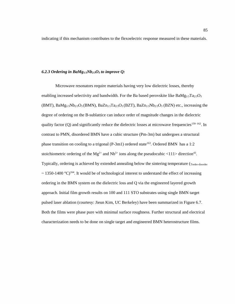
85
indicating if this mechanism contributes to the flexoelectric response measured in these materials.
6.2.3 Ordering in BaMg1/3Nb2/3O3 to improve Q:
Microwave resonators require materials having very low dielectric losses, thereby
enabling increased selectivity and bandwidth. For the Ba based perovskite like BaMg1/3Ta2/3O3
(BMT), BaMg1/3Nb2/3O3 (BMN), BaZn1/3Ta2/3O3 (BZT), BaZn1/3Nb2/3O3 (BZN) etc., increasing the
degree of ordering on the B-sublattice can induce order of magnitude changes in the dielectric
quality factor (Q) and significantly reduce the dielectric losses at microwave frequencies159–162. In
contrast to PMN, disordered BMN have a cubic structure (Pm-3m) but undergoes a structural
phase transition on cooling to a trigonal (P-3m1) ordered state163. Ordered BMN has a 1:2
stoichiometric ordering of the Mg2+ and Nb5+ ions along the pseudocubic <111> direction43.
Typically, ordering is achieved by extended annealing below the sintering temperature (Torder-disorder
~ 1350-1400 °C)164. It would be of technological interest to understand the effect of increasing
ordering in the BMN system on the dielectric loss and Q via the engineered layered growth
approach. Initial film growth results on 100 and 111 STO substrates using single BMN target
pulsed laser ablation (courtesy: Jieun Kim, UC Berkeley) have been summarized in Figure 6.7.
Both the films were phase pure with minimal surface roughness. Further structural and electrical
characterization needs to be done on single target and engineered BMN heterostructure films.

86
Figure 6.7: Growth of pure phase BMN from single target on (a) 001 STO (b) 111 STO (c) film
surface roughness on 111 STO

87
Appendices
Appendix A: RHEED assisted growth of PbMg2/3Nb1/3O3-PbNbO3 heterostructure films
Heterostructure growth was attempted on a RHEED assisted PLD tool on SrRuO3 bottom
electrodes grown on treated (111) SrTiO3 substrates. The growth parameter for epitaxial SrRuO3
thin film has been tabulated in Table A-1, with the RHEED pattern and corresponding roughness
as a function of thickness shown in Figure A-1. Interestingly, the growth transitioned from 3-d to
2-d with increasing thickness.
Figure A-1: RHEED patterns (top) along the <-110> for SrRuO3 grown on 111 STO substrates
with corresponding roughness data obtained from AFM (contact mode)

88
Table A-1: Growth parameters for SrRuO3 and PbMg2/3Nb1/3O3 and PbNbO3 individual layers
PMN growth calibration involved initial film synthesis using the single Mg rich PMN
target on layer by layer grown SrRuO3 using conditions tabulated in Table A-1. Two repeatable
stable RHEED oscillations were observed as shown in Figure A-2, after which islanding
occurred. Next the unit heterostructure growth was attempted, by calculating the number of
pulses corresponding to unit cell of PbMg2/3Nb1/3O3 followed by ablation of the PbNbO3 target.
As seen in Figure A-3, growth of the PbNbO3 layer led to instant islanding in the film. Hence a
timed based synthesis approach was adopted for film growth.
Figure A-2: RHEED oscillations corresponding to Mg rich PMN target
Parameter SrRuO3 PbMg2/3Nb1/3O3/PbNbO3
Temperature 700°C 630°C
Pressure (O2) 100 mTorr 200 mTorr
Laser density 1.5 J/cm2 0.9 J/cm2
Laser frequency 5 Hz 3 Hz

89
Figure A-3: (a) RHEED oscillations corresponding to pulsating Mg rich PMN target and PNO
targets (b) AFM surface roughness data suggesting islanding.
(a)
(b)

90
Appendix B: Growth of heterostructure PMN thin films on different substrates
Two-target PMN heterostructure growth was also achieved on DyScO3, GdScO3 and NdScO3
(101) oriented substrates obtained from CrysTec GmbH, Germany, using timed pulsed laser
deposition to understand the effect of strain induced by the substrate. Ba0.7Sr0.3RuO3 films (~30
nm thick) were epitaxially grown as the bottom electrode on the treated substrates by pulsed laser
deposition, at 1023 K in an oxygen pressure of 200 mTorr, with a laser fluence of 1.3 J/cm2 at a
repetition rate of 3 Hz. Long-range ordered PMN film growth was achieved via subsequent
pulsing of the PbNbO3 and PbMg2/3Nb1/3O3 layers from 1% La doped target batched with 20%
excess Pb at 873 K in an oxygen pressure of 200 mTorr at a laser fluence of 1 J/cm2 and a laser
repetition rate of 3 Hz. The XRD patterns are shown in Figure B-1 and the scanning electron
microscope cross-section images are presented in Figure B-2. As seen from the XRD image, the
films grown on DSO (PMN thickness-75 nm) and GSO (PMN thickness-80 nm) substrates were
relaxed, while the films grown on the NSO substrate (PMN thickness-60-65 nm) was under
tensile strain (0.13 %). As seen from the SEM images, the surface roughness was high on all the
non-STO substrates. Further growth optimization is required for smoother film growths.
Temperature dependent dielectric permittivity-loss (as a function of frequency) and dielectric
Rayleigh characterization (as a function of ac field) results on the different substrates have been
summarized in Figure B-3. Frequency dispersion persisted in all the films, with similar peak in
the irreversible Rayleigh coefficient in the measured temperature range. As shown in Table B-1,
there was a small shift in Tmax and small shift in Tα, max peak in relaxed PMN heterostructure films
on different substrates.

91
Figure B-1: XRD of the two target PMN heterostructure grown on different substrate
Figure B-2: Cross-section SEM images of the two target PMN heterostructure grown on different
substrates

92
Figure B-3: C-D measurement (left) and Rayleigh measurement (right) for two target PMN films
grown on different substrates

93
STO
(PMN
thickness-100
nm)
DSO
(PMN thickness-
75 nm)
GSO
(PMN thickness-
80 nm)
NSO
(PMN thickness-
60-65 nm)
Tmax (at 1 kHz) 250 K 280 K 280 K 240 K
Tα peak 150 K 160 K 170 K 150 K
Table B-1: Summary of Tmax and Tα for two target PMN heterostructure grown on different substrate

94
References
1 S. Trolier-McKinstry and P. Muralt, "Thin film piezoelectrics for MEMS," J.
Electroceramics, 12, 7–17, (2004).
2 F. Li, S. Zhang, D. Damjanovic, L.Q. Chen, and T. Shrout, "Local structural
heterogenity and electromechanical responses of ferroelectrics: learning from relaxor
ferroelectrics," Adv. Funct. Mater., 1801504, 1–21, (2018).
3 L.E. Cross, "Relaxor ferroelectrics: An overview," Ferroelectrics, 151, [1], 305–320,
(1994).
4 A. Bokov and Z.-G. Ye, "Recent progress in relaxor ferroelectrics with perovskite
structure," J. Mater. Sci., 41, [1], 31–52, (2006).
5 Z.G. Ye, "Relaxor ferroelectric complex perovskites: structure, properties and phase
transitions," Key Eng. Mater., 155–156, 81–122, (1998).
6 M. Lejeune and J. Boilot, "PbMg1/3Nb2/3O3 (PMN) multilayer capacitors," J. Phys., 47,
[C1], 895–899, (1986).
7 P. Davies and M. Akbas, "Chemical order in PMN-related relaxors: structure, stability,
modification, and impact on properties," J. Phys. Chem. Solids, 61, [2], 159–166, (2000).
8 P.M. Solomon, B.A. Bryce, M.A. Kuroda, R. Keech, S. Shetty, T.M. Shaw, M. Copel,
L.-W. Hung, A.G. Schrott, C. Armstrong, M.S. Gordon, K.B. Reuter, T.N. Theis, W. Haensch,
S.M. Rossnagel, H. Miyazoe, B.G. Elmegreen, X.-H. Liu, S. Trolier-McKinstry, G.J. Martyna,
and D.M. Newns, "Pathway to the piezoelectronic transduction logic device," Nano Lett., 15, [4],
(2015).
9 T.N. Theis and P.M. Solomon, "It’s time to reinvent the transistor!," Science, 327,
[5973], 1600–1, (2010).
10 D.M. Newns, B.G. Elmegreen, X.-H. Liu, and G.J. Martyna, "The piezoelectronic

95
transistor: A nanoactuator-based post-CMOS digital switch with high speed and low power,"
MRS Bull., 37, [11], 1071–1076, (2012).
11 R.R. Keech, Dimensional Scaling of Perovskite Ferroelectric Thin Films, Pennsylvania
State University, 2016.
12 S. Shetty, A. Damodaran, K. Wang, Y. Yakun, V. Gopalan, L. Martin, S. Trolier-
McKinstry, and 1Department, "Relaxor Behavior in Ordered Lead Magnesium Niobate
(PbMg1/3Nb2/3O3) Thin Films," Adv. Funct. Mater., 04, 258–268, (2018).
13 S. Shetty, J.I. Yang, J. Stitt, and S. Trolier-Mckinstry, "Quantitative and high spatial
resolution d33 measurement of piezoelectric bulk and thin films," J. Appl. Phys., 118, [17],
(2015).
14 G.A. Smolensky, "Physical phenomena in ferroelectrics with diffuse phase transition,"
J. Phys. Soc. Japan, 28, 26–38, (1970).
15 L. Cross, "Relaxor ferroelectrics," Ferroelectrics, 76, [1], 241–267, (1987).
16 A. Burggraaf and C. Stenger, "On diffuse phase transitions," Ferroelectrics, 20, 185–
187, (1978).
17 V. Westphal, W. Kleemann, and M.D. Glinchuk, "Diffuse phase transitions and
random field induced domain states of relaxor ferroelectric PbMg1/3Nb2/3O3," Phys. Rev. Lett., 68,
[6], 847–850, (1992).
18 N. Setter and L.E. Cross, "The contribution of structural disorder to diffuse phase
transitions in ferroelectrics," J. Mater. Sci., 15, [10], 2478–2482, (1980).
19 G.A. Samara, "The relaxational properties of compositionally disordered ABO3
perovskites," J. Phys. Condens. Matter, 15, [9], 367–411, (2003).
20 S.-E. Park and T.R. Shrout, "Ultrahigh strain and piezoelectric behavior in relaxor
based ferroelectric single crystals," J. Appl. Phys., 82, [4], 1804, (1997).
21 F. Li, S. Zhang, T. Yang, Z. Xu, N. Zhang, G. Liu, J. Wang, J. Wang, Z. Cheng, Z.G.

96
Ye, J. Luo, T.R. Shrout, and L.Q. Chen, "The origin of ultrahigh piezoelectricity in relaxor-
ferroelectric solid solution crystals," Nat. Commun., 7, 1–9, (2016).
22 F. Li, S. Zhang, Z. Xu, and L.Q. Chen, "The contributions of polar nanoregions to the
dielectric and piezoelectric responses in domain-engineered relaxor-PbTiO3 Crystals," Adv.
Funct. Mater., 1700310, 1–9, (2017).
23 N. Setter and L.E. Cross, "Role of B-Site cation disorder in diffuse phase transition
behavior of perovskite ferroelectrics.," J. Appl. Phys., 51, [8], 4356–4360, (1980).
24 P. Bonneau, P. Garnier, G. Calvarin, E. Husson, J.R. Gavarri, A.W. Hewat, and A.
Morell, "X-ray and neutron diffraction studies of the diffuse phase transition in ceramics," J.
Solid State Chem., 91, [2], 350–361, (1991).
25 P. Bonneau, P. Garnier, E. Husson, and A. Morell, "Structural study of PMN ceramics
by X-ray diffraction between 297 and 1023 K," Mater. Res. Bull., 24, [2], 201–206, (1989).
26 N. De Mathan, E. Husson, G. Calvarin, and A. Morell, "Structural study of a poled
PbMg1/3Nb2/3O3 ceramic at low temperature," Mat. Res. Bull., 26, [11], 1167–1172, (1991).
27 S. Hong, J. Woo, H. Shin, J.U. Jeon, Y.E. Pak, E.L. Colla, N. Setter, E. Kim, and K.
No, "Principle of ferroelectric domain imaging using atomic force microscope," J. Appl. Phys.,
89, [2], 1377–1386, (2001).
28 X. Zhao, W. Qu, X. Tan, A. Bokov, and Z.-G. Ye, "Electric field-induced phase
transitions in (111)-, (110)-, and (100)-oriented Pb(Mg1∕3Nb2∕3)O3 single crystals," Phys. Rev. B,
75, [10], 104106, (2007).
29 E. V. Colla, E.Y. Koroleva, N.M. Okuneva, and S.B. Vakhrushev, "Long-time
relaxation of the dielectric response in lead magnoniobate," Phys. Rev. Lett., 74, [9], 1681–1684,
(1995).
30 D. Viehland, S.J. Jang, L.E. Cross, and M. Wuttig, "Freezing of the polarization
fluctuations in lead magnesium niobate relaxors," J. Appl. Phys., 68, [6], 2916–2921, (1990).

97
31 A. Levstik, Z. Kutnjak, C. Filipič, and R. Pirc, "Glassy freezing in relaxor ferroelectric
lead magnesium niobate," Phys. Rev. B, 57, [18], 11204–11211, (1998).
32 A. Glazounov and A.K. Tagantsev, "A “breathing” model for the polarization response
of relaxor ferroelectrics," Ferroelectrics, 221, [1], 57–66, (1999).
33 A.E. Glazounov and A.K. Tagantsev, "Crossover in a non-analytical behaviour of
dielectric non-linearity in PbMg1/3Nb2/3O3 relaxor ferroelectric," J. Phys. Condens. Matter, 10,
[39], 8863–8880, (1998).
34 W. Kleemann, "The relaxor enigma — charge disorder and random fields in
ferroelectrics," J. Mater. Sci., 41, [1], 129–136, (2006).
35 W. Kleemann, "Relaxor ferroelectrics: Cluster glass ground state via random fields and
random bonds," Phys. Status Solidi Basic Res., 251, [10], 1993–2002, (2014).
36 C. Randall and A. Bhalla, "Nanostructural-property relations in complex lead
perovskites," Jpn. J. Appl. Phys., 29, [2], 327–333, (1990).
37 C. Randall, D. Barber, R. Whatmore, and P. Groves, "A TEM study of ordering in the
perovskite, Pb(Sc1/2Ta1/2)O3," J. Mater. Sci., 21, [12], 4456–4462, (1986).
38 M.A. Akbas and P.K. Davies, "Domain growth in Pb(Mg1/3Ta2/3)O3 perovskite relaxor
ferroelectric oxides," J. Am. Ceram. Soc., 80, [11], 2933–2936, (1997).
39 M.A. Akbas and P.K. Davies, "Thermally induced coarsening of the chemically
ordered domains in PbMg1/3Nb2/3O3 (PMN)-based relaxors," J. Am. Ceram. Soc., 83, [1], 119–
123, (2000).
40 P.K. Davies and M. Akbas, "Growth of the chemically ordered domains in PMN-type
relaxor ferroelectrics," Ferroelectrics, 221, [1], 27–36, (1999).
41 P.K. Davies, L. Farber, M. Valant, and M.A. Akbas, "Cation ordering and dielectric
properties of PMN-PSN relaxors," AIP Conf. Proc., 535, 38–46, (2000).
42 P.K. Davies and M. Akbas, "Controlling the chemical order in PMN-type relaxors,"

98
MRS Symp. Proc., 541, 425–436, (1999).
43 P.K. Davies, "Cation ordering in complex oxides," J. Solid State Chem., 4, [1999],
467–471, (2000).
44 F. Chu, N. Setter, and a. K. Tagantsev, "The spontaneous relaxor-ferroelectric
transition of Pb(Sc 0.5Ta0.5)O3," J. Appl. Phys., 74, [8], 5129–5134, (1993).
45 D. Fu, H. Taniguchi, M. Itoh, S.Y. Koshihara, N. Yamamoto, and S. Mori, "Relaxor
Pb(Mg1/3Nb2/3)O3: A ferroelectric with multiple inhomogeneities," Phys. Rev. Lett., 103, [20],
2–5, (2009).
46 Y. Yan, S.J. Pennycook, Z. Xu, and D. Viehland, "Determination of the ordered
structures of Pb(Mg1/3Nb2/3O3 and BaMg1/3Nb2/3O3 by atomic-resolution Z-contrast imaging,"
Appl. Phys. Lett., 72, [24], 3145, (1998).
47 H.Z. Jin, J. Zhu, S. Miao, X.W. Zhang, and Z.Y. Cheng, "Ordered domains and polar
clusters in lead magnesium niobate Pb(Mg1/3Nb2/3)O3," J. Appl. Phys., 89, [9], 5048–5052,
(2001).
48 R.A. Cowley, S.N. Gvasaliya, S.G. Lushnikov, B. Roessli, and G.M. Rotaru, "Relaxing
with relaxors: a review of relaxor ferroelectrics," Adv. Phys., 60, [2], 229–327, (2011).
49 F. Chu, I.M. Reaney, and N. Setter, "Role of defects in the ferroelectric relaxor lead
scandium tantalate," J. Am. Ceram. Soc., 78, [7], 1947–1952, (1995).
50 I.W. Chen, P. Li, and Y. Wang, "Structural origin of relaxor perovskites," J. Phys.
Chem. Solids, 57, [10], 1525–1536, (1996).
51 D. Viehland, S.J. Jang, L.E. Cross, and M. Wuttig, "Deviation from Curie-Weiss
behaviour in relaxor ferroelectrics," Phys. Rev. B, 46, [13], 8003, (1992).
52 B.P. Burton, E. Cockayne, S. Tinte, and U. V Waghmare, "First-principles based
simulations of relaxor ferroelectrics," Phase Transitions, 79, [1], 91–121, (2006).
53 S. Wakimoto, C. Stock, Z.-G. Ye, W. Chen, P.M. Gehring, and G. Shirane, "Mode-

99
coupling and polar nanoregions in the relaxor ferroelectric Pb(Mg1/3Nb2/3)O3," Phys. Rev. B, 66,
224102, (2002).
54 A.K. Tagantsev and A.E. Glazounov, "Mechanism of polarization response in the
ergodic phase of a relaxor ferroelectric," Phys. Rev. B, 57, [1], 18–21, (1998).
55 A. Glazounov and A.K. Tagantsev, "Phenomenological model of dynamic nonlinear
response of relaxor ferroelectrics," Phys. Rev. Lett., 85, [10], 2192–5, (2000).
56 X. Zhang, C. Mellinger, E. V. Colla, M.B. Weissman, and D.D. Viehland, "Barkhausen
noise probe of the ferroelectric transition in the relaxor PbMg1/3Nb2/3O3-12%PbTiO3," Phys. Rev.
B, 95, [14], 144203, (2017).
57 R. Pirc and R. Blinc, "Spherical random-bond-random-field model of relaxor
ferroelectrics," Phys. Rev. B, 60, [19], 13470–13478, (1999).
58 R. Pirc, R. Blinc, and V. Bobnar, "Dynamics of relaxor ferroelectrics," Phys. Rev. B -
Condens. Matter Mater. Phys., 63, [5], 1–9, (2001).
59 W. Qu, X. Zhao, and X. Tan, "Evolution of nanodomains during the electric-field-
induced relaxor to normal ferroelectric phase transition in a Sc-doped Pb (Mg13 Nb23) O3
ceramic," J. Appl. Phys., 102, [8], 0–8, (2007).
60 F. Li, D. Lin, Z. Chen, Z. Cheng, J. Wang, C.C. Li, Z. Xu, Q. Huang, X. Liao, L.Q.
Chen, T.R. Shrout, and S. Zhang, "Ultrahigh piezoelectricity in ferroelectric ceramics by design,"
Nat. Mater., 17, 349–354, (2018).
61 B. Dkhil, J.M. Kiat, G. Calvarin, G. Baldinozzi, S.B. Vakhrushev, and E. Suard, "Local
and long range polar order in the relaxor-ferroelectric compounds PbMg1/3Nb2/3O3 and
PbMg0.3Nb0.6Ti0.1O3," Phys. Rev. B - Condens. Matter Mater. Phys., 65, [2], 1–8, (2002).
62 S.-E. Park and T. Shrout, "Characteristics of relaxor-based piezoelectric single crystals
for ultrasonic transducers," IEEE Trans. Ultrason. Ferroelectr. Freq. Control, 44, [5], 1140–1147,
(1997).

100
63 A. Hilton, C. Randall, D. Barber, and T. Shrout, "TEM studies of Pb(Mg1/3 Nb2/3 )O 3 -
PbTiO3 ferroelectric relaxors," Ferroelectrics, 93, [1], 379–386, (1989).
64 D. V. Taylor and D. Damjanovic, "Domain wall pinning contribution to the nonlinear
dielectric permittivity in Pb(Zr, Ti)O[sub 3] thin films," Appl. Phys. Lett., 73, [14], 2045, (1998).
65 D. V Taylor and D. Damjanovic, "Evidence of domain wall contribution to the
dielectric permittivity in PZT thin films at sub-switching fields," 82, [4], 1973–1975, (1997).
66 N. Bassiri-Gharb, I. Fujii, E. Hong, S. Trolier-McKinstry, D. V. Taylor, and D.
Damjanovic, "Domain wall contributions to the properties of piezoelectric thin films," J.
Electroceramics, 19, [1], 49–67, (2007).
67 S. Trolier-McKinstry, N. Bassiri Gharb, and D. Damjanovic, "Piezoelectric
nonlinearity due to motion of 180° domain walls in ferroelectric materials at subcoercive fields:
A dynamic poling model," Appl. Phys. Lett., 88, [20], 202901, (2006).
68 V. Bobnar, Z. Kutnjak, R. Pirc, R. Blinc, and A. Levstik, "Crossover from glassy to
inhomogeneous-ferroelectric nonlinear dielectric response in relaxor ferroelectrics," Phys. Rev.
Lett., 84, [25], 5892–5895, (2000).
69 W. Kleemann, S. Miga, J. Dec, and J. Zhai, "Crossover from ferroelectric to relaxor
and cluster glass in BaTi 1-xZrxO3 (x = 0.25-0.35) studied by non-linear permittivity," Appl.
Phys. Lett., 102, [23], 0–4, (2013).
70 J. Dec, S. Miga, W. Kleemann, and B. Dkhil, "Nonlinear dielectric properties of PMN
relaxor crystals within Landau-Ginzburg-Devonshire approximation," Ferroelectrics, 363, [1],
141–149, (2008).
71 J. Dec, S. Miga, and W. Kleemann, "Ferroelectric Phase Transitions Viewed Via
Nonlinear Dielectric Response," Ferroelectrics, 417, [1], 82–92, (2017).
72 D. Damjanovic, "Ferroelectric , dielectric and piezoelectric properties of ferroelectric
thin films and ceramics," Rep. Prog. Phys., 61, 1267–1324, (1998).

101
73 D. Damjanovic and M. Demartin, "Contribution of the irreversible displacement of
domain walls to the piezoelectric effect in barium titanate and lead zirconate titanate ceramics," J.
Phys. Condens. Matter, 9, 4943–53, (1997).
74 D. Damjanovic, Hysteresis in Piezoelectric and Ferroelectric Materials (2006).
75 D.M. Marincel, "The influence of crystal defects on domain wall motion in thin film
PZT," Ph.D Diss., (2014).
76 D. Damjanovic and M. Demartin, "The Rayleigh law in piezoelectric ceramics," J.
Phys. D. Appl. Phys., 29, [7], 2057–2060, (1996).
77 D. V. Taylor and D. Damjanovic, "Domain wall pinning contribution to the nonlinear
dielectric permittivity in Pb(Zr, Ti)O3 thin films," Appl. Phys. Lett., 73, [14], 2045, (1998).
78 M. Saad, P. Baxter, J. Mcaneney, A. Lookman, L. Sinnamon, P. Evans, A. Schilling, T.
Adams, X. Zhu, R. Pollard, R. Bowman, J. Gregg, D. Jung, F. Morrison, and J. Scott,
"Investigating the effects of reduced size on the properties of ferroelectrics," IEEE Trans.
Ultrason. Ferroelectr. Freq. Control, 53, [12], 2208–2225, (2006).
79 T.M. Shaw, S. Trolier-McKinstry, and P.C. McIntyre, "The properties of ferroelectric
films at small dimension," Annu. Rev. Mater. Sci., 30, 263–298, (2000).
80 E.L. Colla, S. Hong, D. V. Taylor, A.K. Tagantsev, N. Setter, and K. No, "Direct
observation of region by region suppression of the switchable polarization (fatigue) in
Pb(Zr,Ti)O3 thin film capacitors with Pt electrodes," Appl. Phys. Lett., 72, [21], 2763, (1998).
81 F. Griggio and S. Trolier-McKinstry, "Grain size dependence of properties in lead
nickel niobate-lead zirconate titanate films," J. Appl. Phys., 107, [2], 024105, (2010).
82 K.-T. Kim, M.-G. Kang, and C.-I. Kim, "Study on the etching damage characteristics
of PZT thin films after etching in Cl-based plasma," Microelectron. Eng., 71, [3–4], 294–300,
(2004).
83 G.E. Menk, S.B. Desu, W. Pan, and D.P. Vijay, "Dry etching issues in the integration

102
of ferroelectric thin film capacitors," MRS Symp. Proc., 433, 189–200, (1996).
84 W. Pan, C.L. Thio, and S.B. Desu, "Reactive ion etching damage to the electrical
properties of ferroelectric thin films," J. Mater. Res., 13, [02], 362–367, (2011).
85 U. Egger, K. Tomioka, G. Stojakovic, Y. Taniguchi, R. Bruchhaus, H. Zhuang, H.
Kanaya, G. Beitel, and S. Sugimoto, "High temperature plasma etching of PZT capacitor stacks
for high density FERAMs," Mat. Res. Soc. Symp. Proc., 748, 1–6, (2003).
86 P. Werbaneth, J. Almerico, L. Jerde, S. Marks, and B. Wachtmann, "Pt/PZT/Pt and
Pt/barrier stack etches for MEMS devices in a dual frequency high density plasma reactor," 13th
Annu. IEEE/SEMI Adv. Semicond. Manuf. Conf., 177–183, (2002).
87 V. Nagarajan, S.P. Alpay, C.S. Ganpule, B.K. Nagaraj, S. Aggarwal, E.D. Williams,
A.L. Roytburd, and R. Ramesh, "Role of substrate on the dielectric and piezoelectric behavior of
epitaxial lead magnesium niobate-lead titanate relaxor thin films," Appl. Phys. Lett., 77, [3], 438,
(2000).
88 M.D. Nguyen, M. Dekkers, E. Houwman, R. Steenwelle, X. Wan, A. Roelofs, T.
Schmitz-Kempen, and G. Rijnders, "Misfit strain dependence of ferroelectric and piezoelectric
properties of clamped (001) epitaxial Pb(Zr0.52,Ti0.48)O3 thin films," Appl. Phys. Lett., 99, [25],
252904, (2011).
89 V. Nagarajan, A. Roytburd, A. Stanishevsky, S. Prasertchoung, T. Zhao, L. Chen, J.
Melngailis, O. Auciello, and R. Ramesh, "Dynamics of ferroelastic domains in ferroelectric thin
films.," Nat. Mater., 2, [1], 43–7, (2003).
90 V. Nagarajan, "Scaling of the piezoelectric response in ferroelectric nanostructures: An
effective clamping stress model," Appl. Phys. Lett., 87, [24], 242905, (2005).
91 S. Buhlmann, B. Dwir, J. Baborowski, and P. Muralt, "Size effect in mesoscopic
epitaxial ferroelectric structures: Increase of piezoelectric response with decreasing feature size,"
Appl. Phys. Lett., 80, [17], 3195, (2002).

103
92 R. Keech, S. Shetty, M. Kuroda, X. Hu Liu, G.J. Martyna, D.M. Newns, and S. Trolier-
McKinstry, "Lateral scaling of Pb(Mg1/3Nb2/3)O3-PbTiO3 thin films for piezoelectric logic
applications," J. Appl. Phys., 115, [23], 234106, (2014).
93 A. Bernal, A. Tselev, S. Kalinin, and N. Bassiri-Gharb, "Effects of lateral and substrate
constraint on the piezoresponse of ferroelectric nanostructures," Appl. Phys. Lett., 101, [11],
112901, (2012).
94 F. Griggio, S. Jesse, A. Kumar, O. Ovchinnikov, H. Kim, T.N. Jackson, D.
Damjanovic, S. V. Kalinin, and S. Trolier-McKinstry, "Substrate Clamping Effects on
Irreversible Domain Wall Dynamics in Lead Zirconate Titanate Thin Films," Phys. Rev. Lett.,
108, [15], 157604, (2012).
95 M. Wallace, R.L. Johnson-Wilke, G. Esteves, C.M. Fancher, R.H.T. Wilke, J.L. Jones,
and S. Trolier-McKinstry, "In situ measurement of increased ferroelectric/ferroelastic domain
wall motion in declamped tetragonal lead zirconate titanate thin films," J. Appl. Phys., 117,
054103, (2015).
96 D. Fu, H. Taniguchi, M. Itoh, and S. Mori, Pb(Mg1/3Nb2/3)O3 (PMN) Relaxor: Dipole
Glass or Nano-Domain Ferroelectric?, InTech, (2012).
97 M. Yoshida, S. Mori, N. Yamamoto, Y. Uesu, and J.M. Kiat, "Transmission electron
microscope observation of relaxor ferroelectric," J. Korean Phys. Soc., 32, 993–995, (1998).
98 P. Hirsch, A. Howie, R. Nicholson, D. Pashley, and M. Whelan, Electron Microscopy
of Thin Crystals (1965).
99 E. Garboczi, K. Snyder, J. Douglas, and M. Thorpe, "Geometrical percolation threshold
of overlapping ellipsoids," Phys. Rev. E, 52, [1], 819–828, (1995).
100 I.-K. Jeong, T.W. Darling, J.K. Lee, T. Proffen, R.H. Heffner, J.S. Park, K.S. Hong,
W. Dmowski, and T. Egami, "Direct observation of the formation of polar nanoregions in
Pb(Mg1/3 Nb 2/3)O3 Using neutron pair distribution function analysis," Phys. Rev. Lett., 94, [14],

104
147602, (2005).
101 K. Lefki and G.J.M. Dormans, "Measurement of piezoelectric coefficients of
ferroelectric thin films," J. Appl. Phys., 76, [3], 1764, (1994).
102 M.J. Cabral, S. Zhang, E.C. Dickey, and J.M. LeBeau, "Gradient chemical order in the
relaxor Pb(Mg 1∕3 Nb 2∕3 )O 3," Appl. Phys. Lett., 112, [8], 082901, (2018).
103 A.K. Tagantsev and A.E. Glazounov, "Mechanism of polariztion response and
dielectric non linearity of PMN relaxor ferroelectric," Phase Transitions, 65, [1–4], 117–139,
(1998).
104 X. Zhao, "Development of long range cation order and its impact on dielectric
properties in Pb(Mg1/3Nb2/3)O3 based relaxor ferroelectrics," Ph.D Diss., Iowa State University
(2008).
105 E. V. Colla, N. Jurik, Y. Liu, M. Delgado, M. Weissman, D.D. Viehland, and Z. Ye, "
Kinetics and thermodynamics of the ferroelectric transitions in PbMg1/3Nb2/3O3 and
PbMg1/3Nb2/3O3-12% PbTiO3 crystals," Journal of Applied Physics 113, 184104 (2013.)
106 E. V. Colla, D. Vigil, J. Timmerwilke, M.B. Weissman, D.D. Viehland, and B. Dkhil,
"Stability of glassy and ferroelectric states in the relaxors PbMg1/3Nb2/3O3 and PbMg1/3Nb2/3O3 -
12% PbTiO3," Phys. Rev. B - Condens. Matter Mater. Phys., 75, [21], 1–6, (2007).
107 S. Hashemizadeh and D. Damjanovic, "Nonlinear dynamics of polar regions in
paraelectric phase of (Ba 1-x ,Sr x )TiO 3 ceramics," Appl. Phys. Lett., 110, [19], 192905, (2017).
108 R. Pirc, R. Blinc, and Z. Kutnjak, "Nonlinear dielectric response of relaxor
ferroelectrics," Phys. Rev. B, 65, 1–7, (2002).
109 S.S.N. Bharadwaja, E. Hong, S.J. Zhang, L.E. Cross, and S. Trolier-McKinstry,
"Nonlinear dielectric response in (1−x)Pb(Zn1∕3Nb2∕3)O3-xPbTiO3 (x=0.045 and 0.08) single
crystals," J. Appl. Phys., 101, [10], 104102, (2007).
110 J. Dec, W. Kleemann, S. Miga, C. Filipic, A. Levstik, R. Pirc, T. Granzow, and R.

105
Pankrath, "Probing polar nanoregions in Sr0 . 61 Ba0 . 39 Nb2 O6 via second-harmonic dielectric
response," Phys. Rev. B, 3–6, (2003).
111 K. Lefki and G.J.M. Dormans, "Measurement of piezoelectric coefficients of
ferroelectric thin films," J. Appl. Phys., 76, [3], 1764, (1994).
112 A.L. Kholkin, C. Wutchrich, D. V. Taylor, and N. Setter, "Interferometric
measurements of electric field-induced displacements in piezoelectric thin films," Rev. Sci.
Instrum., 67, [5], 1935, (1996).
113 L. Chen, J.-H. Li, J. Slutsker, J. Ouyang, and A. Roytburd, "Contribution of substrate
to converse piezoelectric response of constrained thin films," J. Mater. Res., 19, [10], 2853–2858,
(2011).
114 S. Lepadatu, M. Stewart, and M.G. Cain, "Quantification of electromechanical
coupling measured with piezoresponse force microscopy," J. Appl. Phys., 116, [6], 066806,
(2014).
115 M. Stewart, S. Lepadatu, L.N. McCartney, M.G. Cain, L. Wright, J. Crain, D.M.
Newns, and G.J. Martyna, "Electrode size and boundary condition independent measurement of
the effective piezoelectric coefficient of thin films," APL Mater., 3, [2], 026103, (2015).
116 S. Sivaramakrishnan, P. Mardilovich, A. Mason, A. Roelofs, T. Schmitz-Kempen, and
S. Tiedke, "Electrode size dependence of piezoelectric response of lead zirconate titanate thin
films measured by double beam laser interferometry," Appl. Phys. Lett., 103, [13], 132904,
(2013).
117 P. Gerber, A. Roelofs, C. Kugeler, U. Bottger, R. Waser, and K. Prume, "Effects of
the top-electrode size on the piezoelectric properties (d33 and S) of lead zirconate titanate thin
films," J. Appl. Phys., 96, [5], 2800, (2004).
118 Q.M. Zhang, W.Y. Pan, and L.E. Cross, "Laser interferometer for the study of
piezoelectric and electrostrictive strains," J. Appl. Phys., 63, [8], 2492, (1988).

106
119 J.E. Graebner, B.P. Barber, P.L. Gammel, D.S. Greywall, and S. Gopani, "Dynamic
visualization of subangstrom high-frequency surface vibrations," Appl. Phys. Lett., 78, [2], 159,
(2001).
120 W.Y. Pan and L.E. Cross, "A sensitive double beam laser interferometer for studying
high-frequency piezoelectric and electrostrictive strains," Rev. Sci. Instrum., 60, [8], 2701,
(1989).
121 J.-F. Li, P. Moses, and D. Viehland, "Simple, high-resolution interferometer for the
measurement of frequency-dependent complex piezoelectric responses in ferroelectric ceramics,"
Rev. Sci. Instrum., 66, [1], 215, (1995).
122 Z. Huang and R.W. Whatmore, "A double-beam common path laser interferometer for
the measurement of electric field-induced strains of piezoelectric thin films," Rev. Sci. Instrum.,
76, [12], 123906, (2005).
123 M.G. Cain, M. Stewart, and M. Downs, in NSTI-Nanotech (2006), pp. 670–673.
124 C. Chao, Z. Wang, W. Zhu, and O. Tan, "Scanning homodyne interferometer for
characterization of piezoelectric films and microelectromechanical systems devices," Rev. Sci.
Instrum., 76, [6], 063906, (2005).
125 Z. Huang, Q. Zhang, S. Corkovic, R. Dorey, F. Duval, G. Leighton, R. Wright, P.
Kirby, and R.W. Whatmore, "Piezoelectric PZT films for MEMS and their characterization by
interferometry," J. Electroceramics, 17, [2–4], 549–556, (2006).
126 R. Herdier, D. Jenkins, E. Dogheche, D. Remiens, and M. Sulc, "Laser Doppler
vibrometry for evaluating the piezoelectric coefficient d33 on thin film," Rev. Sci. Instrum., 77,
[9], 093905, (2006).
127 A. Kholkin, S. Kalinin, A. Roelofs, and A. Gruverman, in Scanning Probe Microsc.
Electr. Electromechanical Phenom. Nanoscale (Springer Science+Business Media, New York,
2007).

107
128 O. Kuffer, I. Maggio-Aprile, J.-M. Triscone, O. Fischer, and C. Renner, "Piezoelectric
response of epitaxial Pb(Zr0.2Ti0.8)O3 films measured by scanning tunneling microscopy," Appl.
Phys. Lett., 77, [11], 1701, (2000).
129 F. Xu, F. Chu, and S. Trolier-McKinstry, "Longitudinal piezoelectric coefficient
measurement for bulk ceramics and thin films using pneumatic pressure rig," J. Appl. Phys., 86,
[1], 588, (1999).
130 J. Lazar, O. Číp, M. Čížek, J. Hrabina, and Z. Buchta, "Suppression of air refractive
index variations in high-resolution interferometry.," Sensors, 11, [8], 7644–55, (2011).
131 G. Peggs and A. Yacoot, "A review of recent work in sub-nanometre displacement
measurement using optical and X-ray interferometry," Phil. Trans. R. Soc. Lond. A, 360, 953–
968, (2002).
132 T. Jungk, Á. Hoffmann, and E. Soergel, "Influence of the inhomogeneous field at the
tip on quantitative piezoresponse force microscopy," Appl. Phys. A, 86, [3], 353–355, (2006).
133 T. Jungk, Á. Hoffmann, and E. Soergel, "Challenges for the determination of
piezoelectric constants with piezoresponse force microscopy," Appl. Phys. Lett., 91, [2007], 8–
11, (2007).
134 S. Kalinin, A. Rar, and S. Jesse, "A decade of piezoresponse force microscopy:
progress, challenges, and opportunities," IEEE Trans. Ultrason. Ferroelectr. Freq. Control, 53,
[12], 2226–2252, (2006).
135 G. Zavala, J.H. Fendler, and S. TrolierMcKinstry, "Characterization of ferroelectric
lead zirconate titanate films by scanning force microscopy," J. Appl. Phys., 81, [11], 7480–7491,
(1997).
136 E. Soergel, "Piezoresponse force microscopy (PFM)," J. Phys. D. Appl. Phys., 44,
[46], 464003, (2011).
137 S. Jesse, A.P. Baddorf, and S. V Kalinin, "Dynamic behaviour in piezoresponse force

108
microscopy," Nanotechnology, 17, [6], 1615–1628, (2006).
138 S. Jesse, A. Kumar, S. V Kalinin, A. Gannepali, and R. Proksch, "Band excitation
scanning probe microscopies : traveling through the Fourier Space," Asylum Res, [Application
note 16], 2–5, (2010).
139 F. Mammano and J.F. Ashmore, "A laser interferometer for sub-nanometre
measurements in the cochlea," J. Neurosci. Methods, 60, [1–2], 89–94, (1995).
140 L. Deck and P. de Groot, "High-speed noncontact profiler based on scanning white-
light interferometry.," Appl. Opt., 33, [31], 7334–8, (1994).
141 A. Safari and E.K. Akdogan, editors , Piezoelectric Transducers and Acoustic
Materials for Transducer Applications (Springer Science+Business Media, 2007).
142 R.L. Johnson-wilke, R.H.T. Wilke, M. Wallace, A. Rajashekhar, G. Esteves, Z.
Merritt, J.L. Jones, and S. Trolier-mckinstry, "Ferroelectric / Ferroelastic domain wall motion in
dense and porous tetragonal lead zirconate titanate films," IEEE Trans. Ultrason. Ferroelectr.
Freq. Control, 62, [1], 46–55, (2015).
143 F. Chu, F. Xu, J. Shepard, and S. Trolier-McKinstry, in Mater. Res. Soc. Symp. Proc.
493, (1998), pp. 409–414.
144 S.H. Baek, J. Park, D.M. Kim, V. Aksyuk, R.R. Das, S.D. Bu, D. Felker, J. Lettieri, V.
Vaithyanathan, S.S.N. Bharadwaja, N. Bassiri-Gharb, Y.B. Chen, H.P. Sun, C.M. Folkman, H.W.
Jang, D.J. Kreft, S.K. Streiffer, R. Ramesh, X.Q. Pan, S. Trolier-McKinstry, D.G. Schlom, M.S.
Rzchowski, R.H. Blick, and C.B. Eom, "Giant piezoelectricity on Si for hyperactive MEMS.,"
Science, 334, [6058], 958–61, (2011).
145 R. Keech, L. Ye, J.L. Bosse, G. Esteves, J. Guerrier, J.L. Jones, M.A. Kuroda, B.D.
Huey, and S. Trolier-McKinstry, "Declamped piezoelectric coefficients in patterned 70/30 lead
magnesium niobate–lead titanate thin films," Adv. Funct. Mater., 27, [9], (2017).
146 M. Wallace, R. Johnson-Wilke, G. Esteves, C. Fancher, R. Wilke, J. Jones, and S.

109
Trolier-McKinstry, "In situ measurement of increased ferreoelectric/ferroelastic domain wall
motion in declamped tetragonal lead zirconate titanate thin films," To be published, (2015).
147 F. Griggio, S. Jesse, a. Kumar, O. Ovchinnikov, H. Kim, T.N. Jackson, D.
Damjanovic, S. V. Kalinin, and S. Trolier-McKinstry, "Substrate Clamping Effects on
Irreversible Domain Wall Dynamics in Lead Zirconate Titanate Thin Films," Phys. Rev. Lett.,
108, [15], 157604, (2012).
148 P. Zubko, G. Catalan, and A.K. Tagantsev, "Flexoelectric effect in solids," Annu. Rev.
Mater. Res., 43, [1], 387–421, (2013).
149 W. Ma and L.E. Cross, "Flexoelectric polarization of barium strontium titanate in the
paraelectric state," Appl. Phys. Lett., 81, [18], 3440–3442, (2002).
150 W. Ma and L.E. Cross, "Large flexoelectric polarization in ceramic lead magnesium
niobate," Appl. Phys. Lett., 79, [26], 4420, (2001).
151 J.Y. Fu, W. Zhu, N. Li, and L.E. Cross, "Experimental studies of the converse
flexoelectric effect induced by inhomogeneous electric field in a barium strontium titanate
composition," J. Appl. Phys., 100, [2006], 024112, (2006).
152 J. Narvaez and G. Catalan, "Origin of the enhanced flexoelectricity of relaxor
ferroelectrics," Appl. Phys. Lett., 104, [16], 162903, (2014).
153 L.M. Garten and S. Trolier-McKinstry, "Enhanced flexoelectricity through residual
ferroelectricity in barium strontium titanate," J. Appl. Phys., 117, [9], 094102, (2015).
154 A. Biancoli, C.M. Fancher, J.L. Jones, and D. Damjanovic, "Breaking of macroscopic
centric symmetry in paraelectric phases of ferroelectric materials and implications for
flexoelectricity," Nat. Mater., 14, [2], 224–229, (2014).
155 J.Y. Fu, W. Zhu, N. Li, and L.E. Cross, "Experimental studies of the converse
flexoelectric effect induced by inhomogeneous electric field in a barium strontium titanate
composition," J. Appl. Phys., 100, [2], 024112, (2006).

110
156 J.Y. Fu and L.E. Cross, "Separate control of direct and converse piezoelectric effects
in flexoelectric piezoelectric composites," Appl. Phys. Lett., 91, [2007], 89–92, (2007).
157 S. Baskaran, S. Thiruvannamalai, H. Heo, H.J. Lee, S.M. Francis, N. Ramachandran,
and J.Y. Fu, "Converse piezoelectric responses in nonpiezoelectric materials implemented via
asymmetric configurations of electrodes," J. Appl. Phys., 108, [6], 064116, (2010).
158 L. Shu, W. Huang, S. Ryung Kwon, Z. Wang, F. Li, X. Wei, S. Zhang, M. Lanagan,
X. Yao, and X. Jiang, "Converse flexoelectric coefficient f1212 in bulk Ba0.67Sr0.33TiO3," Appl.
Phys. Lett., 104, [23], 232902, (2014).
159 S.B. Desu and H.M. O’Bryan, "Microwave Loss Quality of BaZn1/3Ta2/3O3Ceramics,"
J. Am. Ceram. Soc., 68, [10], 546–551, (1985).
160 P.K. Davies, J. Tong, and T. Negas, "Effect of Ordering-Induced Domain Boundaries
on Low-Loss Ba(Zn1/3Ta2/3)O3-BaZrO3 Perovskite Microwave Dielectrics," J. Am. Ceram. Soc.,
80, [7], 1727–1740, (1997).
161 H. Hughes, D.M. Iddles, and I.M. Reaney, "Niobate-based microwave dielectrics
suitable for third generation mobile phone base stations," Appl. Phys. Lett., 79, [18], 2952–2954,
(2001).
162 A. Dias and R.L. Moreira, "Far-infrared spectroscopy in ordered and disordered
BaMg1/3Nb2/3O3 microwave ceramics," J. Appl. Phys., 94, [5], 3414–3421, (2003).
163 R.L. Moreira, F.M. Matinaga, and A. Dias, "Raman-spectroscopic evaluation of the
long-range order in Ba(B′1/3B″2/3)O3 ceramics," Appl. Phys. Lett., 78, [4], 428–430, (2001).
164 B. Burton and E. Cockayne, "Why Pb(B,B′)O3 perovskites disorder at lower
temperatures than Ba(B,B′)O3 perovskites," Phys. Rev. B, 60, [18], R12542–R12545, (1999).

VITA
Smitha Shetty
Smitha Shetty was born in India on December 30, 1981. She got her undergraduate
degree in Electrical Engineering from the University of Mumbai in India in 2003. She received
two Master’s degree in Electrical and Computer Engineering from University of South Florida
(2005) and Carnegie Mellon University (2007). She spent four years in a start-up technology
company working on the process development and characterization of pyroelectric FPGA
infrared detectors. She decided to go back to school for her doctorate degree in Materials Science
and Engineering in 2012 under the guidance of Prof. Susan Trolier-McKinstry. Dr. Shetty
received her Ph.D. in Spring 2019.