ElectroMagnetic Compatibility in Power Electronics: from ...
22
• 1 ElectroMagnetic Compatibility in Power Electronics: from packaging to EMC filter optimization JL.Schanen, Professor University Grenoble Alps Clustering and Global Challenges (CGC2021)
Transcript of ElectroMagnetic Compatibility in Power Electronics: from ...

• 1
ElectroMagnetic Compatibility in Power Electronics: from
packaging to EMC filter optimization
JL.Schanen, ProfessorUniversity Grenoble Alps
Clustering and Global Challenges (CGC2021)

Introduction
40% of electricity processed by power electronics
Expected doubling over the next decade, reaching up to 80% by 2030
Impact of Wide Bandgap revolution
Spec Consortium, Singapore
Power Electronics
Transportation
Buildings
Industry
Healthcare
Consumer Electronics
RenewableEnergy
Clustering and Global Challenges (CGC2021) • 2/22

Introduction
• High efficiency• Low volume, weight• High dynamic
• ElectromagneticInterferences
Clustering and Global Challenges (CGC2021) • 3/22

Outline
1. EMI generation principle
2. EMC & Semiconductor Packaging
3. EMC Filter design and optimization
4. EMC models at system level
EMC: ElectroMagnetic Compatibility
EMI: ElectroMagnetic Interferences
Clustering and Global Challenges (CGC2021) • 4/22

1. EMI Generation Principle
High speed Switching
dI/dt, dV/dt
Ground current – Common ModeStray Capacitance
Grid
Differential Mode
Radiated
emissions
Clustering and Global Challenges (CGC2021) • 5/22

1. EMI Generation Principle
CM/DM definitionI1
I2
V2
V1Icm Vcm
Vdm
1 2dmV V V 1 2
2cm
V VV
1 2
2dm
I II
1 2cmI I I
1 1
2 2
1 1
2 2out in
V V
V VMat
I I
I I
outin
outinmc
mc
md
md
I
I
V
V
P
I
V
I
V
/2
1
2
1
/
1100
002
1
2
12
1
2
100
0011
P
Z1
Z3
Z2
Z23 Z4
Z5 Z6
Vin1
Vin2
Iin1
Iin2
Vout1
Vout2
Iout1
Iout2
1
md md
md md
mc mc
mc mcout in
V V
I IP Mat P
V V
I I
If Z2=Z3
And Z5=Z6
0
0
DM
CM
CM/DM independence if symmetry
Clustering and Global Challenges (CGC2021) • 6/22

Stray inductance:
Voltage overshoot & ringing
C
Simplified driver
Stray inductance (switching loop)
Source
Gate
Drain
Vds
Vgs UT
Rg
DV=L.di/dt
di/dt
2. EMC & Semiconductor Packaging
𝑧 = ൗ𝑅 2 . ൗ𝐶𝑜𝑠𝑠𝐿𝑠𝑡𝑟𝑎𝑦
Reduced DV: 50A/ns*5nH 250V!
Increased damping
Clustering and Global Challenges (CGC2021) • 7/22

• Stray capacitances & CM generation
C
MOSFETSource
Gate
Drain
Vds
Vgs UT
Rg
Stray capacitance
to the ground
Cdg
Cpg
Cmg
Cpg Cmg Cdg
Floating point
Icm
External CM generation
Internal
recyclingVds
2. EMC & Semiconductor Packaging
Clustering and Global Challenges (CGC2021) • 8/22

• Stray capacitances & CM generationWarning: if Cpg Cmg: possible CM generation
𝐼𝐶𝑝𝑔 = 𝐶𝑝𝑔𝑑∆𝑉
𝑑𝑡= −𝐼𝐶𝑚𝑔
C
Source
Gate
Drain
Vds
Vgs UT
Rg
Stray capacitance
to the ground
Cdg
Cpg
Cmg
DV
DV
Only if Cpg=Cmg
2. EMC & Semiconductor Packaging
Clustering and Global Challenges (CGC2021) • 9/22

2. EMC & Semiconductor Packaging
Example of G2ELab recent result:
Power Chip on Chip applied to GaN devices
Clustering and Global Challenges (CGC2021) • 10/22

𝑑𝑉
𝑑𝑡
G
Huge Common Mode
current generation!!!
2. EMC & Semiconductor Packaging
Shielding middle point
Clustering and Global Challenges (CGC2021) • 11/22

2. EMC & Semiconductor Packaging
Shielding middle point𝑑𝑉
𝑑𝑡
G
Most of Common Mode
current is recirculating
inside converterClustering and Global Challenges (CGC2021) • 12/22

3. EMC Filter design and optimization
Design by optimization of EMC Filter
converterFilter (CM & DM)Normalized grid (LISN)
Line-Ground Voltage
monitored
Clustering and Global Challenges (CGC2021) • 13/22

3. EMC Filter design and optimization
1 current source: current discontinuity
1 voltage source: voltage swing
C
ESL
ESRCpm
Design by optimization of EMC Filter:
Frequency model of the converter
Clustering and Global Challenges (CGC2021) • 14/22
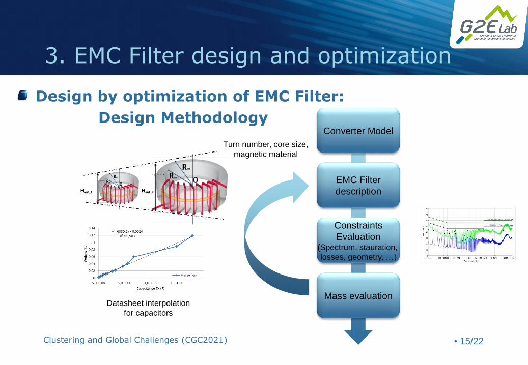
3. EMC Filter design and optimization
Design by optimization of EMC Filter:
Design MethodologyConverter Model
EMC Filter
description
Constraints
Evaluation(Spectrum, stauration,
losses, geometry, …)
Mass evaluation
Turn number, core size,
magnetic material
Datasheet interpolation
for capacitors
Clustering and Global Challenges (CGC2021) • 15/22

3. EMC Filter design and optimization
Design by optimization of EMC Filter: impact of Fsw
Clustering and Global Challenges (CGC2021) • 16/22

3. EMC Filter design and optimization
Design by optimization of EMC Filter: impact of floatingpoint capacitance on the filter
Cpm[pF] Cpm[pF]
Cut off frequency of CM filter [kHz]
Clustering and Global Challenges (CGC2021) • 17/22

3. EMC Filter design and optimization
Variation of standard (DO160)
Clustering and Global Challenges (CGC2021) • 18/22

4. EMC models at system level
Usual EMC approach: standardized grid (LISN) and standardized emission level
System optimization: real grids, computation of EMI level, comparison with disturbance level
Need of EMC models at system level
Filter 3 Converter 3
Filter 1 Converter 1 Filter 2 Converter 2 Filter n
Filter x Converter x
Sou
rce
Clustering and Global Challenges (CGC2021) • 19/22

4. EMC models at system level
Black Box / Terminal Model Identification process
Off-line impedance measurement
Line current measurement in a known
configuration (LSIN)Clustering and Global Challenges (CGC2021) • 20/22

4. EMC models at system level
Model validation in several configurations (exp results)
I1 – Minus to ground I2 – EMC FilterClustering and Global Challenges (CGC2021) • 21/22

Conclusion
EMC as "dark side of Power Electronics"
Wide Bandgap devices leads EMC issue more critical
EMI reduction at packaging level
Subnanohenry requirement
Reduced Floating Point capacitance, local shielding
Symmetry
EMC filter optimization
Not straightforward phenomena
Technologically dependent
Proposed Design by Optimization methodology allows variousstudies (impact of technology, standards, …)
EMC model at system level
Future challenge of embedded grids ?
• 22/22Clustering and Global Challenges (CGC2021)