electrodes Low Contact Resistancef for AlGaN/GaN structure with Nitrogen Vacancy … ·...
42
TiSi 2 electrodes Low Contact Resistancef for AlGaN/GaN structure with Nitrogen Vacancy by SiO 2 Supervisor: Prof. Hiroshi Iwai Tokyo Institute of Technology Department of Electrical and Electronic Engineering 09_05126 Mari Okamoto AlGaN/GaN attracts attention as power device material. To realize high performance of AlGaN/GaN device, there are still matters to be solved. High contact resistance is one of the issues. Aluminum(Al) and Titanium(Ti) are commonly used as ohmic contact metal material. Ti can form nitrogen vacancies at AlGaN layer, which is essential for ohmic contact. However, narrow process parameter can only realize low contact resistance. This is why Ti causes crystal defect at AlGaN by high-temperature annealing. So we proposed TiSi 2 contact. Si has control over forming crystal defect and we get ohmic contact resistance and area ratio resistance. And so far, it is reported that SiO 2 can also form nitrogen vacancies by high temperature. So, we combine SiO 2 forming nitrogen vacancies and TiSi 2 which has low metal function to realize low ohmic contact. 1
Transcript of electrodes Low Contact Resistancef for AlGaN/GaN structure with Nitrogen Vacancy … ·...

TiSi2 electrodes Low Contact Resistancef for AlGaN/GaN structure with Nitrogen
Vacancy by SiO2
Supervisor: Prof. Hiroshi Iwai
Tokyo Institute of Technology
Department of Electrical and Electronic Engineering
09_05126 Mari Okamoto
AlGaN/GaN attracts attention as power device material. To realize high performance of
AlGaN/GaN device, there are still matters to be solved. High contact resistance is one of
the issues. Aluminum(Al) and Titanium(Ti) are commonly used as ohmic contact metal
material. Ti can form nitrogen vacancies at AlGaN layer, which is essential for ohmic
contact. However, narrow process parameter can only realize low contact resistance.
This is why Ti causes crystal defect at AlGaN by high-temperature annealing. So we
proposed TiSi2 contact. Si has control over forming crystal defect and we get ohmic
contact resistance and area ratio resistance.
And so far, it is reported that SiO2 can also form nitrogen vacancies by high
temperature. So, we combine SiO2 forming nitrogen vacancies and TiSi2 which has low
metal function to realize low ohmic contact.
1

Contents
1 Introduction
1.1 Situation of saving energy…………………………………….…...5
1.2 Reason of GaN………………………………………………….….6
1.3 Issues of GaN………………………………………………………7
1.4 Currently GaN contact in use………………………………………8
1.5 Necessary conditions for lowering contact resistance……………...9
1.6 Approach to main subject…………………………………………11
Reference
2 Experiment
2.1 Experimental procedure
2.2 Experimental principle
2.2.1 SPM cleaning and HF treatment………………………………15
2.2.2 SiO2 deposition by TEOS……………………………………...16
2.2.3 Lithography…………………………………………………….16
2.2.4 Wet etching with BHF………………………………………….17
2.2.5 RF magnetron sputtering……………………………………….19
2.2.6 Dry etching by RIE……………………………………………..19
2.2.7 I-V measurement………………………………………………..19
Reference
2

3 Results and Discussion with Nitrogen Vacancy with
SiO2
3.1 XPS measurement…………………………………………………27
3.2 Analysis of interface between AlGaN and SiO2…………………...28
3.3 I-V measurement with SiO2 capped annealing……………………..29
4Result and Discussion with TiSi2 and Ti
4.1 Comparison with Ti and TiSi2……………………………….…….34
4.2 Analysis interface TiSi2 and AlGaN………………………….……36
4.3 Dependence on annealing temperature……………………….…….38
5 Conclusion and Future issues………………………….……40
Acknowledgement………………………………………………....40
3

Chapter 1
Introduction
1.1 Situation of saving energy
1.2 Reason of GaN
1.3 Issues of GaN
1.4 Currently GaN contact in use
1.5 Necessary conditions for lowering contact resistance
1.6 Approach to main subject
1.7 Structure of the Thesis
Reference
4

1.1 Situation of saving energy
Recently, some environmental problems, such as global warming, become more serious.
On the other hand, the consumption of energy per head and also in our country goes on
increasing. The table1.1 shows that electric energy is the most consumed. [1.1] So it is
the key to the saving energy that we use electric energy efficiently.
Now, electric power changing technology takes a big roll in electric power flow from
power plant to consumers. [1.2] So, we need to develop energy changing technology
high efficiently. And, there are some devices marked as power device material such as
SiC and GaN. This table1.1 shows the reason why SiC or GaN are suitable for power
device material. [1.3]
Table 1.1 Physical property of Si, SiC, GaN used as a power electric
semiconductor.
So, high electron mobility and saturated velocity cause high frequency switching,
and high breakdown field and thermal conductivity cause high power and high
temperature operation. [1.4]
5

1.2 Reason of selecting GaN
Epitaxial layer of GaN is commonly grown on sapphire however epitaxial layer
can be grown on Si substrate by MOCVD(Metal Organic Chemical Vapor
Deposition). The price of Si substrate (about 80yen/cm2) is much more lower
than sapphire (480yen/cn2), so price per unit of GaN substrate can be also
lower.[1.5] Furthermore, This achievement enabled AlGaN/GaN device to
construct lateral FET(Field-Effect-Transistor) and many devices can be produced
on large area substrate. Now, the size of GaN on Si is enlarged to substrate
six-inch caliber. [1.6]
However, it is not facilitated for high quality epitaxial layer of GaN to grow on
Si substrate. When epitaxial layer is grown, AlN layer is necessary as a buffer
layer for difference of mismatching thermal and lattice coefficient GaN on Si has
high thermal conductivity and conductivity control.[1.7] So a GaN device has the
performance of about ten MOS-FET, we realize miniaturization and weight
saving of AlGaN/GaN device.
6

1.3 Issues of AlGaN and GaN device
There are still some issues to realize to go on the market. For example, one of
the issues is normally-on transistor. Figure 1.3.1 shows normally-on state, minus
threshold voltage causes that transistor
is on state unless gate voltage is plus
value. [1.8] This result from 2DEG(2
Dimensional Electron Gas) of
AlGaN/GaN structure which shows
Figure1.3.2. Normally-on state is
necessary for safety in a high current or
power electricity used in industry. On
the other hand, one of the most important issues of AlGaN/GaN device is high
contact resistance. However contact resistance is in general 10-8 cm2 on silicon
substrate, contact resistance on GaN/AlGaN substrate is 10-5cm2.[1.9] High
contact resistance causes power loss and less efficiency. In this report we pay
attention with contact resistance.
I[A]
[V]0
Normally-on state
Figure 0.1.3.1 Normally on state
Metal
ALGaN
GaN
2DEG
Fig 2.1.3 band figure of AlGaN/GaN with metal
7
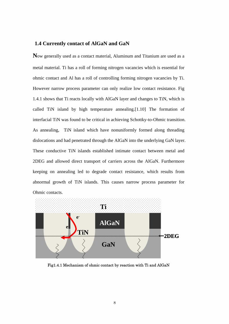
1.4 Currently contact of AlGaN and GaN
Now generally used as a contact material, Aluminum and Titanium are used as a
metal material. Ti has a roll of forming nitrogen vacancies which is essential for
ohmic contact and Al has a roll of controlling forming nitrogen vacancies by Ti.
However narrow process parameter can only realize low contact resistance. Fig
1.4.1 shows that Ti reacts locally with AlGaN layer and changes to TiN, which is
called TiN island by high temperature annealing.[1.10] The formation of
interfacial TiN was found to be critical in achieving Schottky-to-Ohmic transition.
As annealing, TiN island which have nonuniformly formed along threading
dislocations and had penetrated through the AlGaN into the underlying GaN layer.
These conductive TiN islands established intimate contact between metal and
2DEG and allowed direct transport of carriers across the AlGaN. Furthermore
keeping on annealing led to degrade contact resistance, which results from
abnormal growth of TiN islands. This causes narrow process parameter for
Ohmic contacts.
AlGaN
GaN
TiN
Ti
e-
e-
←2DEG
AlGaN
GaN
TiN
Ti
e-
e-
←2DEG
Fig1.4.1 Mechanism of ohmic contact by reaction with Ti and AlGaN
8

1.5 Necessary conditions for lowering contact resistance
To form ohmic contact, there are some necessary conditions. First, it is critical
for choosing low metal function. Fig.1.4.1 shows typical metal and its function
used as a material of metal electrode on AlGaN/GaN. [1.11]
4.9NiSi
4.7TiSi2
4.7TiN
4.52W
4.45Mo
4.14Ti
4.13Al
Work Function[eV]Material
4.9NiSi
4.7TiSi2
4.7TiN
4.52W
4.45Mo
4.14Ti
4.13Al
Work Function[eV]Material
Table.1.4.1 material and its work function
Fig.1.4.2 shows that low work function of metal leads to ohmic contact.
MetalALGaN
GaN
Metal function m
MetalALGaN
GaN
Metal function m
MetalALGaN
GaN
✖
MetalALGaN
GaN
✖
MetalALGaN
GaN
Fig 1.4.2 Mechanism of current between metal and GaN
Electrons in metal can easily flow into GaN layer for selecting low metal function.
Second, band bending is also necessary for ohmic contact.Fig.1.4.3 shows that
tunneling current occurred by band bending.
9

Metal AlGaN GaN
✖ ✖
Metal AlGaN GaN
✖ ✖
MetalAlGaN
GaNMetalAlGaN
GaN
Fig1.4.3 Mechanism of tunneling current between metal and GaN
Wide depletion region cannot flow tunneling current however band bending
causes to narrow depletion region and tunneling current applied. Band bending is
occurred by heavy doping on interface of semiconductor and applying H2-plasma
cleaning. This report proves that AlGaN and SiO2 reacts with each other and n+
layer was formed in AlGaN layer, which causes band bending and realize ohmic
contact. [1.12]
Finally, narrow AlGaN layer can also realize tunneling current by etching AlGaN
layer physically with H2-plasma etching and CH4,H2,Ar plasma.[1.13] So plasma
etching enables to cause tunneling current.
10

1.6 Approach to main subject
By measuring I-V characteristic and analyzing XPS result, we observed and
considered reaction with SiO2 and AlGaN or TiSi2 and AlGaN. So, this
observation leads to find mechanism of the reason that TiSi2 can get ohmic
contact.
11

Reference
[1.1]Agency for Natural Resources and Energy: ‘The white paper on energy
usage’ the second chapter (2011)
[1.2]L.M.tollbert, T.J.King, B.Ozepinec :’Power Electronics For Distributed
Energy Systems and Transmission and Distribution Applications’ The University
of Tennessee-Knoxville. (2005)
[1.3]VE Chelnokov, AL Syrkin:’Overview of SiC power electronics’, Elecron
Device, IEEE (1989)
[1.4]M.Hikita, M.managahara: ’GaN-Based Devices’, Panasonic Technical
Journal Vol.55(2009)
[1.5]Pierre Gibart, ’Metal organic vapour phase epitaxy of GaN and lateral
overgrowth’, Institute of Physics Pubilishing. (2004)
[1.6]D.Zhu, C.Mcaleese: ’GaN-LEDs grown on 6-inch diameter Si(111)
substarates by MOVPE’ Proc. Of SPIE Vol.7231
[1.7]M.Sakai, K.Asano: ‘Grownth of AlGaN/GaN Heterostructure Grown on
Epitaxial AlN/Sappire Templates by MOVPE’ (2002)
[1.8]N.Ikeda, Li Jiang :’Novel GaN Device for High-Power Application with
Thin AlGaN/GaN Heterostructure Layer.’(2008)
[1.9]Bin Lu, D.Piedra, T.palacios: ‘GaN Power Electronics’Advanced
Semiconductor Devices (2010)
[1.10]Liang Wang, Titih M.Mohammed, ’Formation mechanism of Ohmic
contacts on AlGaN/GaN heterostructure Electrical and microstructure
characterizations’ Journal of Applied physics (2008)
12

[1.11]M,Kanamura, T.Oki, T.Kikkawa: ‘GaN-HEMT Technology for Future
Applications’Fujitsu. 60,5 (2009)
[1.12] Y. Taur, T. H. Ning: “Fundamentals of MODERN VLSI DEVICES”,,
Cambridge University Press (1998)
[1.13]T.Hasizume, H.Hasegawa: ‘Effects of nitrogen deficiency on electronic properties
of AlGaN surfaces subjected to thermal and plasma process.’ RCIQE(2004)
13

Chapter 2
Experiment
2.1 Experimental procedure
2.2 Experimental principle
2.2.1 SPM cleaning and HF treatment
2.2.2 SiO2 deposition by TEOS
2.2.3 Lithography
2.2.4 Wet etching with BHF
2.2.5 RF magnetron sputtering
2.2.6 Dry etching by RIE
2.2.7 I-V measurement
Reference
14

2.1 Experimental procedure
Fig. 2,1 shows experimental procedure of contact. Contact was fabricated on
AlGaN(26nm) on GaN(1.3um). The silicon-die-oxide(100nm) was deposited
by plasma-TEOS sputtering. And SiO2 and AlGaN layer were cut down by
RIE(Reactive Ion Etching). The silicon-nitride(50nm) was deposited by
magnetron sputtering and successively SiO2(100nm) was deposited after
photolithography. The samples were annealed at 1000 for 10 min. SiO2. The
SiO2 was removed by BHF and metal layer such as TiSi2, TiN and Ti for
electrode was deposited by magnetron sputtering. Finally, metal layers were
removed by RIE and the samples were I-V measured.
・・・・・・・・・・・・・・・・・・・・・・・・・・・・・・・・・・・・・・・・・・・・・・・・・・・・・・・・・・・・・・Chapter [2.2.6]
・・・・・・・・・・・・・・・・・・・・・・・・・・・・・・・・・・・・・・・・・・・・・・・・・・・・・・・・・・・・・・・・・・・・・・・・・・・・・・・・・・・・・・Chapter [2.2.3]
SPM,HF last treatment ・・・・・・・・・・・・・・・・・・・・・・・・・・・・・・・・・・・・・・・・・・・・・・・・・・・・・・・・・・・・Chapter [2.2.1]
・・・・・・・・・・・・・・・・・・・・・・・・・・・・・・・・・・・・・・・・・・・・・・・・・・・・・・・・・・・Chapter [2.2.2]
・・・・・・・・・・・・・・・・・・・・・・・・・・・・・・・・・・・・・・・・・・・・・・・・・・・・・・・・・・・・・・・・・・・・Chapter [2.2.4]
・・・・・・・・・・・・・・・・・・・・・・・・・・・・・・・・・・・・・・・・・・・・・・・・・・・・・・・・・・・・・・・・・・・Chapter [2.2.5]
Photolithography
Wet etching by BHF
・・・・・・・・・・・・・・・・・・・・・・・・・・・・・・・・・・・・・・・・・・・・・・・・・・・Chapter [2.2.7]
Lithography, Dry etching by RIE(Cl2)
TiN/TiSi2 deposition by TEOS
TiN/Ti deposition by TEOS
IV mesurement
Annealing
・・・・・・・・・・・・・・・・・・・・・・・・・・・・・・・・・・・・・・・・・・・・・・・・・・・・・・・・・・・・・・・・・・・・・・・・Chapter [2.2.8]
SiO2 deposition by TEOS
Dry etching by RIE(Cl2)
SiO2 deposition by TEOS
Photolithography, Wet etching by BHF
Fig.2.1 Experimental procedure of contact
15

2.2 Experimental principle
2.2.1 SPM cleaning and HF treatment
Particles and organic substance at the surface of Si substrate become a cause of false
operation. Therefore, it is important to clean the surface of Si substrate. SPM cleaning is
one of the effective cleaning methods. The cleaning liquid is made from H2O2 and
H2SO4 (H2O2:H2SO4 = 1:4). Because of its oxidizability, particles and organic
substance are oxidized and separated from the surface of Si substrate. However, the
surface of Si substrate is oxidized and SiO2 is formed during SPM cleaning. 1% HF is
used to eliminate the SiO2.
2.2.2 SiO2 deposition by using TEOS
TEOS(tetraethoxysilane) is usually used for depositing SiO2 and as a gate insulator
material in semiconductor.[2.1] Here, we deposited SiO2 on samples for covering
AlGaN layer in isolation. By CVD(chemical vapor deposition) method using TEOS gas,
SiO2 layer with which O2 gas reacts can be formed rapidly and at low temperature.
The plasma CVD method is described below. First, oxygen gas and TEOS gas used as
material gases are injected into reactor. Applying high frequency electric field generates
plasma which makes gases excited. Excited atoms are reacted chemically and deposited.
TEOS is commonly reacted with SiH4, O2 and Ar, however, we use CF4, O2 and Ar in
this report. Deposition temperature is 200°C and deposition rate is 5nm/min. We
deposited 100nm for 20min.
16

Process Gases O2RF power
By-products to the pump
Heater
Plasma
Process Gases O2Process Gases O2RF power
By-products to the pump
Heater
Plasma
Fig.2.2 2.1 Schematic illustration of RIE
CH
H H
H
O
H
C CO
H H
H
H
H
C
C H
H
H
O
HC
H
Si
C H
O
H
H
HC
H
CH
H H
H
O
H
CCH
H H
H
O
H
C CO
H H
H
H
H
CCO
H H
H
H
H
C
C H
H
H
O
HC
H C H
H
H
O
HCC
H
SiSi
C H
O
H
H
HC
H C H
O
H
H
HCC
H
CH
H H
H
O
H
C CO
H H
H
H
H
CSi
C H
O
H
H
HC
H
Sisub
CH
H H
H
O
H
CCH
H H
H
O
H
C CO
H H
H
H
H
CCO
H H
H
H
H
CSi
C H
O
H
H
HC
H C H
O
H
H
HCC
H
Sisub
CH
HH
H
O
H
C CO
HH
HHH
C
Si
C H
O
H
H
HC
H
Si
sub
CH
HH
H
O
H
C CO
HH
HHH
C
Si
C H
O
H
H
HC
HC
H
HH
H
O
H
CC
H
HH
H
O
H
C CO
HH
HHH
CC
OH
H
HHH
C
Si
C H
O
H
H
HC
H C H
O
H
H
HCC
H
Si
sub
CH
H H
H
O
H
C CO
H H
H
H
H
C
C H
H
H
O
HC
H
Si
C H
O
H
H
HC
H
CH
H H
H
O
H
CCH
H H
H
O
H
C CO
H H
H
H
H
CCO
H H
H
H
H
C
C H
H
H
O
HC
H C H
H
H
O
HCC
H
SiSi
C H
O
H
H
HC
H C H
O
H
H
HCC
H
CH
H H
H
O
H
C CO
H H
H
H
H
CSi
C H
O
H
H
HC
H
Sisub
CH
H H
H
O
H
CCH
H H
H
O
H
C CO
H H
H
H
H
CCO
H H
H
H
H
CSi
C H
O
H
H
HC
H C H
O
H
H
HCC
H
Sisub
CH
HH
H
O
H
C CO
HH
HHH
C
Si
C H
O
H
H
HC
H
Si
sub
CH
HH
H
O
H
C CO
HH
HHH
C
Si
C H
O
H
H
HC
HC
H
HH
H
O
H
CC
H
HH
H
O
H
C CO
HH
HHH
CC
OH
H
HHH
C
Si
C H
O
H
H
HC
H C H
O
H
H
HCC
H
Si
sub
Fig 2.2.2.2 Transformation of TEOS by CVD method
2.2.3 Rapid thermal annealing
Rapid thermal annealing (RTA) was used for produce of nitrogen vacancies. The heat
chamber was vacuum and filled in nitrogen gas, so that the effect of prevention
oxidation of the sample. The samples were annealed by infrared ray for 1 minute.
17

2.2.4 Lithography
Photolithography is a process used in microfabrication to pattern the substrate. [2.2] On
the substrate, the liquid called “resist” which has photosensitivity was put on. The resist
has two types, “positive type” and “negative type”. The former type is that the part of
substrate irradiated with ultraviolet rays is removed by liquid developer. We use this
type. After exposure , the substrates are soaked in liquid developer and baked on the
heater at 150℃ for 10min to stabilize resist.
Mask
Resist
Ultraviolet
Positive type Negative type
Fig.2.2.4 Different process with negative type and positive type
18

2.2.5 Wet etching by BHF
Buffered HF (BHF) are used for wet etching process. When the RE-oxides uncovered
with resist are etched, HCl is used as etching liquid which is called etchant. When the
SiO2 is etched, BHF is used as etchant.
2.2.6 Dry etching by RIE
Reactive ion etching (RIE) is one of the patterning methods. Etching gas becomes the
plasma in a similar way with RF sputtering. However, RIE is not only physical but also
chemical reaction. For etching of aluminum-gallium-nitride and silicon-die-oxide,
chemistry is used as etching gas in this study. The aluminum-gallium-nitride and
silicon-die-oxide which are uncovered with resist reacts with Cl- and becomes SiCl4
andAlCl3 which are gas at room temperature.[2.3] When the resist is eliminated, O2 is
used as etching gas and this process is called ashing.
2.2.7 RF magnetron sputtering
Titanium which is used as contact electrode in this study is deposited by radio
frequency (RF) magnetron sputtering with Ar gas.[2.4] An RF with 13.56 MHz at a
power of 150 W is applied between substrate side and target (Ti) side. Because of the
difference of mass, Ar ions and electrons are separated. A magnet is set underneath the
target, so that the plasma damage is minimized. Electrons run through the circuit from
substrate side to target side, because substrate side is subjected to be conductive and
target side is subjected to be insulated. Then, target side is biased minus and Ar ions hit
the target.
19

In this study, silicon is also used as a target and titanium and Fig .2.3 shows that silicon
are laminated by changing targets for appropriate time and at low power of 80W
Fig.2.2 Schematic illustration of RF magnetron sputtering
Fig.2.3 lamination layer of TiSi2
20

2.2.8 I-V measurement method
TLM is short for Transmission Line Model. It is usually used as a method for
evaluating I-V measurement and Contact resistance. [2.5]
The contact resistance measurement technique was shown in Fig.2.4.
ZW
d
I I
Fig .2.4 Contact resistance structure. The contact width and length
are Z and L and the diffusion width is W.
To measure I-V characteristic is needed for determining contact resistance. I-V
characteristic is measured by applying voltage on electrodes with variable electrode
distances. Fig.2.5 shows relation between total resistance and the distance between
electrodes.
2
Fig .2.5 Total resistance and distances between electrodes
21
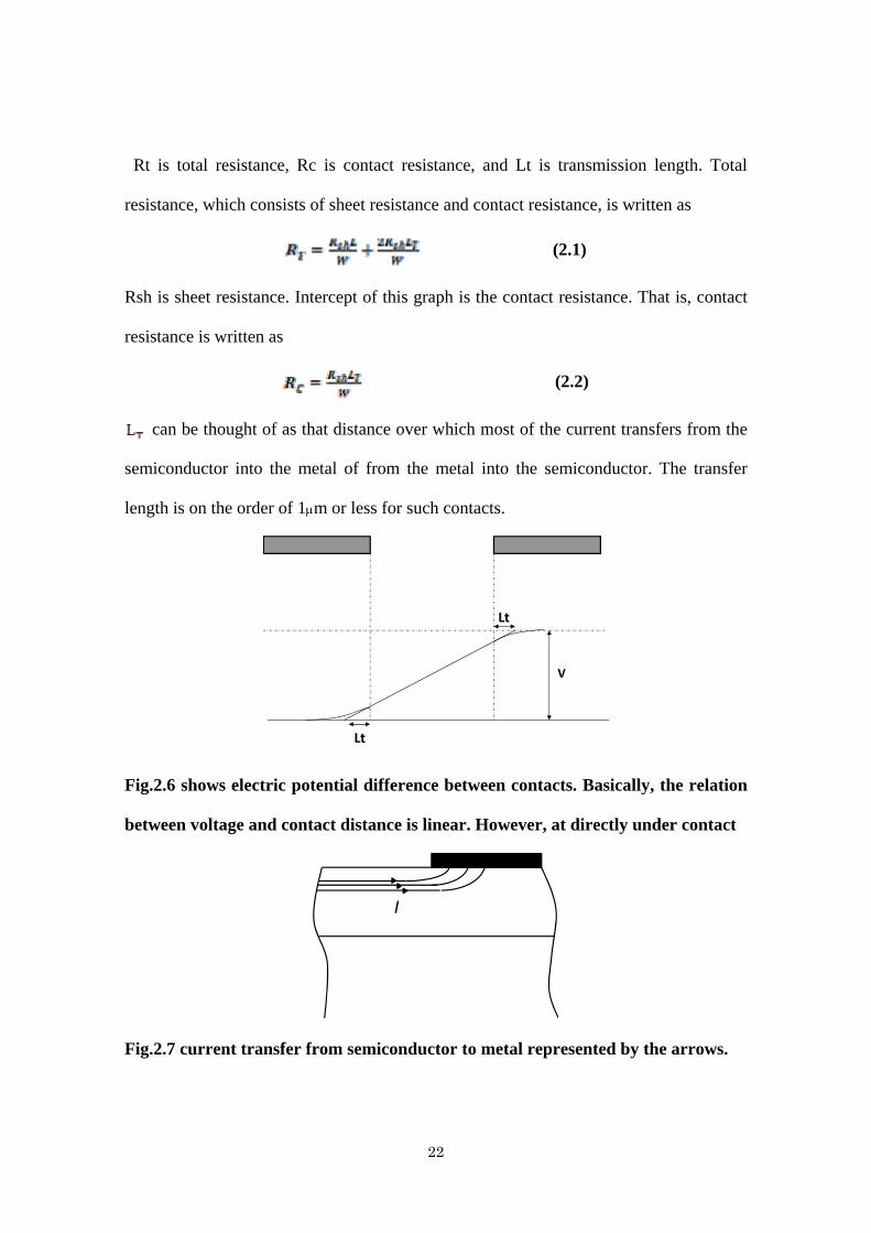
Rt is total resistance, Rc is contact resistance, and Lt is transmission length. Total
resistance, which consists of sheet resistance and contact resistance, is written as
(2.1)
Rsh is sheet resistance. Intercept of this graph is the contact resistance. That is, contact
resistance is written as
(2.2)
can be thought of as that distance over which most of the current transfers from the
semiconductor into the metal of from the metal into the semiconductor. The transfer
length is on the order of 1m or less for such contacts.
Lt
Lt
V
Fig.2.6 shows electric potential difference between contacts. Basically, the relation
between voltage and contact distance is linear. However, at directly under contact
I
Fig.2.7 current transfer from semiconductor to metal represented by the arrows.
22

340m
250m
290m
300m80m
290m60m
40m
320m
150m340m
250m
290m
300m80m
290m60m
40m
320m
150m
Fig.2.8 mask pattern used in the process
23

GaN
AlGaN
GaN
AlGaN
SiO2
GaN
AlGaN
SiO2
GaN
AlGaN
GaN
AlGaN
SiO2
GaN
AlGaN
SiO2
GaN
AlGaN
SiO2
GaN
AlGaN
GaN
AlGaN
GaN
AlGaN
SiO2
GaN
AlGaN
SiO2
GaN
AlGaN
GaN
AlGaN
SiO2
GaN
AlGaN
GaN
AlGaN
GaN
AlGaN
GaN
AlGaNSiO2
GaN
AlGaNSiO2
GaN
AlGaNSiO2
GaN
AlGaN
GaN
AlGaNSiO2
GaN
AlGaNSiO2
TiSi2/TiN
GaN
AlGaNSiO2
GaN
AlGaNSiO2
GaN
AlGaN
GaN
AlGaNSiO2
TiSi2/TiN
GaN
AlGaNSiO2
TiSi2/TiN
GaN
AlGaN
GaN
AlGaNSiO2
TiSi2/TiN
GaN
AlGaNSiO2
GaN
AlGaNSiO2
GaN
AlGaN
GaN
AlGaNSiO2
I-V measurement
I II I
GaN
AlGaN
GaN
AlGaN
SiO2
GaN
AlGaN
SiO2
GaN
AlGaN
GaN
AlGaN
SiO2
GaN
AlGaN
SiO2
GaN
AlGaN
SiO2
GaN
AlGaN
GaN
AlGaN
GaN
AlGaN
SiO2
GaN
AlGaN
SiO2
GaN
AlGaN
GaN
AlGaN
SiO2
GaN
AlGaN
GaN
AlGaN
GaN
AlGaN
GaN
AlGaNSiO2
GaN
AlGaNSiO2
GaN
AlGaNSiO2
GaN
AlGaN
GaN
AlGaNSiO2
GaN
AlGaNSiO2
TiSi2/TiN
GaN
AlGaNSiO2
GaN
AlGaNSiO2
GaN
AlGaN
GaN
AlGaNSiO2
TiSi2/TiN
GaN
AlGaNSiO2
TiSi2/TiN
GaN
AlGaN
GaN
AlGaNSiO2
TiSi2/TiN
GaN
AlGaNSiO2
GaN
AlGaNSiO2
GaN
AlGaN
GaN
AlGaNSiO2
I-V measurement
I II I
Fig 2.8 Schematic illustration of contact process.
24

Reference
[2.1] Alex Lubnin: ‘SiO2 TEOS-OZONE CVD’ DUMIC symposium(1998)
[2.2]H.Levinson: ‘Principles Of Lithography’p402-405(2005)
[2.3]N.Hayasaka: ‘Method for removing composite attached to material by dry
etching’(1994)
[2.4] Hari Singh Nalwa: ‘Handbook of Thin Films’Five-VoloumeSet, p410-p421.(2001)
25

Chapter 3
Results and Discussion
with Nitrogen vacancy
with SiO2
3.1 XPS measurement
3.2 Analysis of interface between AlGaN and SiO2
3.3 I-V measurement with SiO2 capped annealing
26

3.1 XPS measurement
XPS(X-ray photoelectron Spectroscopy) is one of the spectroscopic technique which
measures elemental composition .Because it uses high energy X-ray as exciting light, it
is possible to excite a core electron which strongly bound to an atom and to emit
photoelectron. Each material has their own core electron binding energy. It is quite
different between materials each other. Therefore, the information which atom is caused
can be known after core electron binding energy is analyzed and the peak of that is
measured. We can perform quantitative analysis by comparing with peak intensity. To
determine exactly binding energy, that of Si in the sample is set to the standard, and that
of other material is measured relate to a standard.
Focusing Electron Gun
X‐ray
Focusing MonochromaterCrystal
Hemispherical Electron Energy Analyzer
Fast MultichanneDtector
Figure3.1.1 Schematic illustration of XPS
27

3.2 Analysis of interface between AlGaN and SiO2
Figure3.1.2 shows analysis sample A and B by XPS measurements. A is the sample
which was processed by SPM cleaning and HF cleaning. B is processed by SPM and
HF cleaning and annealed at 1000°C for 10min in N2 ambientafter deposition with SiO2
layer. An x-ray energy of 8keV was used as a source for XPS. So that photoelectrons as
deep as 40 nm can be collected.
1559 1561 15621560 1563 1564 1565
Inte
nsi
ty[a
.u.]
Binding Energy[eV]
0.2eV
Al1s without SiO2 capped annealing
(h=7940eV, TOA=80o)
Al1s with SiO2 capped annealing
1559 1561 15621560 1563 1564 1565
Inte
nsi
ty[a
.u.]
Binding Energy[eV]
0.2eV
1559 1561 15621560 1563 1564 15651559 1561 15621560 1563 1564 1565
Inte
nsi
ty[a
.u.]
Binding Energy[eV]
0.2eV
Al1s without SiO2 capped annealing
(h=7940eV, TOA=80o)
Al1s with SiO2 capped annealing
Figure 3.2.1 Al1s spectrum of the sample with and without SiO2 capped annealing
The Figure shows that Al 1s peak shift into high energy band by 0.2 keV. Fig3.2.2
shows that This result indicates that nitrogen vacancy is formed at AlGaN and Al
changes into AlN, which make n+ layer formed. That proved that SiO2 layer can form
28

nitrogen vacancy by high temperature annealing.
Metal
ALGaN
GaN
2DEG
vvMetal
ALGaN
GaN
2DEG
vv
Fig 3.2.2 Band structure with annealing
3.3 I-V measurement with annealed SiO2
Figure 3.3.1 shows I-V measurement of the sample which is processed with annealing at
1000oC for 1min after SiO2 deposited and annealed for 1min at from 0oC to 950oC.
This result shows that less current flows with the higher annealing temperature is.
950OC
asdepo
-5 -2 -1-3-4 0 1 2 3 4 5
2.0
0.5
1.0
1.5
0.0
-0.5
-1.0
-1.5
-2.0
Cur
rentm
Voltage [V]
950OC
asdepo
-5 -2 -1-3-4 0 1 2 3 4 5-5 -2 -1-3-4 0 1 2 3 4 5
2.0
0.5
1.0
1.5
0.0
-0.5
-1.0
-1.5
-2.0
2.0
0.5
1.0
1.5
0.0
-0.5
-1.0
-1.5
-2.0
Cur
rentm
Voltage [V]
Fig 3.3.1 I-V measurement with SiO2 capped annealing at asdepo and 950oC
29

Figure 3.3.2 shows I-V measurement of the sample which is processed without
annealing and annealed for 1min at from 0oC to 950oC. Different from result of SiO2
capped annealing, current flow increases with high temperature annealing for the
sample without SiO2 capped annealing.
-5 -2 -1-3-4 0 1 2 3 4 5
2.0
0.5
1.0
1.5
0.0
-0.5
-1.0
-1.5
-2.0
Voltage [V]
Cur
rentm
asdepo
950OC
-5 -2 -1-3-4 0 1 2 3 4 5
2.0
0.5
1.0
1.5
0.0
-0.5
-1.0
-1.5
-2.0
Voltage [V]
Cur
rentm
asdepo
950OC
Fig 3.3.2 I-V measurement without SiO2 capped annealing at asdepo and 950oC
Figure 3.3.3 shows Relationships with Total resistance and annealing temperature. This
results also with high temperature annealing
30

Annealing temperature [OC]
Tot
al R
esis
tanc
e TiSi2 with SiO2 capped annealing
TiSi2 with SiO2 capped annealing
1.41.21.00.80.60.40.20.0
0 500 600400300 700 800 900 9500 500 600400300 700 800 900 950
1.41.21.00.80.60.40.20.0
0 500 600400300 700 800 900 9500 500 600400300 700 800 900 950
Annealing temperature [OC]
Tot
al R
esis
tanc
e TiSi2 with SiO2 capped annealing
TiSi2 with SiO2 capped annealing
1.41.21.00.80.60.40.20.0
0 500 600400300 700 800 900 9500 500 600400300 700 800 900 950
1.41.21.00.80.60.40.20.0
0 500 600400300 700 800 900 9500 500 600400300 700 800 900 950
Fig 3.3.3 Relationships with total resistance and annealing temperature of the
samples with SiO2-capped annealing and without annealing.
This result indicates that the samples with SiO2-capped annealing at low temperature
can get the lower contact resistance than the samples without SiO2-capped annealing.
Figure3.3.4 shows I-V measurement of the samples which is processed with and
without SiO2-capped annealing at asdepo state
-5 -2 -1-3-4 0 1 2 3 4 5
2.0
0.5
1.0
1.5
0.0
-0.5
-1.0
-1.5
-2.0
TiSi2 with SiO2 capped annealing
TiSi2 with SiO2 capped annealing
Cur
rentm
Voltage [V]-5 -2 -1-3-4 0 1 2 3 4 5-5 -2 -1-3-4 0 1 2 3 4 5
2.0
0.5
1.0
1.5
0.0
-0.5
-1.0
-1.5
-2.0
2.0
0.5
1.0
1.5
0.0
-0.5
-1.0
-1.5
-2.0
TiSi2 with SiO2 capped annealing
TiSi2 with SiO2 capped annealing
Cur
rentm
Voltage [V]
Fig 3.3.4 I-V measurement with and without SiO2 capped annealing at asdepo state
31

From this result that is the sample with SiO2 capped annealing has lower total resistance
than the sample without SiO2 capped annealing, it is considered that nitrogen vacancy is
formed at AlGaN layer by depositing SiO2 and annealed.
32

Chapter 4
Results and Discussion
with Contact of TiSi2
4.1 Comparison with Ti and TiSi2
4.2 Analysis interface TiSi2 and AlGaN
4.3 Dependence on annealing time
33

4.1 Comparison with Ti and TiSi2
Chapter 3 shows SiO2 can form nitrogen vacancy, on the other hand the samples
without SiO2 capped annealing gets ohmic contact of TiSi2. So we use TiSi2 electrode
and measured I-V characteristic without SiO2 capped annealing. Compared with TiSi2,
Ti(50nm) was deposited as a contact material and measured I-V characteristic as well as
TiSi2 by annealing for 1min and N2 ambient.
Figure 4.1.1 shows I-V measurement of Ti with annealing at 700oC to 950OC.
-5 -2 -1-3-4 0 1 2 3 4 5
2.0
0.5
1.0
1.5
0.0
-0.5
-1.0
-1.5
-2.0
Cur
rentm
Voltage [V]
950℃
900℃
850℃
800℃750℃
700℃
300m
150m
80m
-5 -2 -1-3-4 0 1 2 3 4 5
2.0
0.5
1.0
1.5
0.0
-0.5
-1.0
-1.5
-2.0
Cur
rentm
Voltage [V]-5 -2 -1-3-4 0 1 2 3 4 5-5 -2 -1-3-4 0 1 2 3 4 5
2.0
0.5
1.0
1.5
0.0
-0.5
-1.0
-1.5
-2.0
2.0
0.5
1.0
1.5
0.0
-0.5
-1.0
-1.5
-2.0
Cur
rentm
Voltage [V]
950℃
900℃
850℃
800℃750℃
700℃
300m
150m
80m
300m
150m
80m
Fig 4.1.1 I-V measurement of Ti annealed from 750oC to 950oC
This result indicates that ohmic contacts were formed at 750OC annealing. The higher
temperature annealed more than 750OC, the less current flows.
I-V measurement of TiSi2 is shown in Fig 4.1.2.
34

-5 -2 -1-3-4 0 1 2 3 4 5
2.0
0.5
1.0
1.5
0.0
-0.5
-1.0
-1.5
-2.0
Cur
rentm
Voltage [V]
850℃800℃
750℃
700℃
950℃
900℃
300m
150m
80m
-5 -2 -1-3-4 0 1 2 3 4 5
2.0
0.5
1.0
1.5
0.0
-0.5
-1.0
-1.5
-2.0
Cur
rentm
Voltage [V]-5 -2 -1-3-4 0 1 2 3 4 5-5 -2 -1-3-4 0 1 2 3 4 5
2.0
0.5
1.0
1.5
0.0
-0.5
-1.0
-1.5
-2.0
2.0
0.5
1.0
1.5
0.0
-0.5
-1.0
-1.5
-2.0
Cur
rentm
Voltage [V]
850℃800℃
750℃
700℃
950℃
900℃
300m
150m
80m
Fig 4.1.2 I-V measurement of TiSi2 annealed from 750oC to 950oC
This result indicates that ohmic contacts were formed at 950oC annealing. The higher
temperature annealing caused that current flow is increasing from 700oC to 950oC. Then,
Fig 4.1.3 shows total resistance dependency on of TiSi2 electrode with contact distance
with annealed at 950oC in N2 ambient.
4000 150 20010050 250 300 350
Distance between contacts(m)
Tot
alre
sist
ance
(m
m)
0.18
0.16
0.14
0.12
0.1
0.08
0.06
0.04
0.02
04000 150 20010050 250 300 350
Distance between contacts(m)
Tot
alre
sist
ance
(m
m)
0.18
0.16
0.14
0.12
0.1
0.08
0.06
0.04
0.02
0
Fig4.1.3 Relation with Total resistance of TiSi2 and distance between contacts
35
So, ohmic contact of TiSi2 is proportional of specific area. Using TLM method and
contact specific resistance is c=9.6E-4[cm]
Contact resistance is lowere, however this contact resistance needs improvement for
reducing contact resistance.
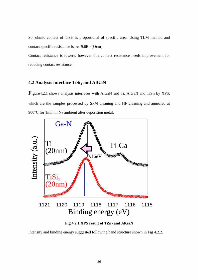
4.2 Analysis interface TiSi2 and AlGaN
Figure4.2.1 shows analysis interfaces with AlGaN and Ti, AlGaN and TiSi2 by XPS,
which are the samples processed by SPM cleaning and HF cleaning and annealed at
900°C for 1min in N2 ambient after deposition metal.
Binding energy (eV)1115111611171118111911201121
Inte
nsit
y (a
.u.)
Ti(20nm)
TiSi2(20nm)
Ti-Ga
Ga-N
0.16eV
Binding energy (eV)1115111611171118111911201121
Inte
nsit
y (a
.u.)
Ti(20nm)
Ti-Ga
Ga-N
0.16eV
TiSi2(20nm)
Fig 4.2.1 XPS result of TiSi2 and AlGaN
Intensity and binding energy suggested following band structure shown in Fig 4.2.2.
36

Fig 4.2.2 Band structure with TiSi2, AlGaN and GaN with annealing
This XPS result of Ti and TiSi2 and band structure indicate that TiSi2 can generate
nitrogen vacancy at AlGaN layer and band bending. Especially XPS result supposed
that Ti forms alloy such as TiGa, however TiSi2 doesn’t make alloy and reacts with
AlGaN layer over the entire surface.
4.3 Dependence on annealing temperature
The samples which of metal are Ti and TiSi2 were annealed at 950OC and each I-V
characteristic was measured by changing annealing time from 1min to 20 min. This
result is shown in Fig 4.3.1 and Fig 4.3.2. Fig 4.3.1 shows I-V measurement of Ti and
Fig 4.3.2 shows I-V measurement of TiSi2.
37

-5 -2 -1-3-4 0 1 2 3 4 5
2.0
0.5
1.0
1.5
0.0
-0.5
-1.0
-1.5
-2.0
Cur
rentm
Voltage [V]
1min
5min
20min
10min
40min 60min
300m
150m
80m
300m
150m
80m
-5 -2 -1-3-4 0 1 2 3 4 5
2.0
0.5
1.0
1.5
0.0
-0.5
-1.0
-1.5
-2.0
Cur
rentm
Voltage [V]
1min
5min
20min
10min
40min 60min
-5 -2 -1-3-4 0 1 2 3 4 5
2.0
0.5
1.0
1.5
0.0
-0.5
-1.0
-1.5
-2.0
Cur
rentm
Voltage [V]-5 -2 -1-3-4 0 1 2 3 4 5-5 -2 -1-3-4 0 1 2 3 4 5
2.0
0.5
1.0
1.5
0.0
-0.5
-1.0
-1.5
-2.0
2.0
0.5
1.0
1.5
0.0
-0.5
-1.0
-1.5
-2.0
Cur
rentm
Voltage [V]
1min
5min
20min
10min
40min 60min
300m
150m
80m
300m
150m
80m
Fig 4.3.1 I-V measurement of Ti with annealing for 1min to 60min
-5 -2 -1-3-4 0 1 2 3 4 5
2.0
0.5
1.0
1.5
0.0
-0.5
-1.0
-1.5
-2.0
Cur
rentm
Voltage [V]
1min
5min
20min
10min
40min 60min
300m
150m
80m
300m
150m
80m
-5 -2 -1-3-4 0 1 2 3 4 5
2.0
0.5
1.0
1.5
0.0
-0.5
-1.0
-1.5
-2.0
Cur
rentm
Voltage [V]
1min
5min
20min
10min
40min 60min
-5 -2 -1-3-4 0 1 2 3 4 5
2.0
0.5
1.0
1.5
0.0
-0.5
-1.0
-1.5
-2.0
Cur
rentm
Voltage [V]-5 -2 -1-3-4 0 1 2 3 4 5-5 -2 -1-3-4 0 1 2 3 4 5
2.0
0.5
1.0
1.5
0.0
-0.5
-1.0
-1.5
-2.0
2.0
0.5
1.0
1.5
0.0
-0.5
-1.0
-1.5
-2.0
Cur
rentm
Voltage [V]
1min
5min
20min
10min
40min 60min
300m
150m
80m
300m
150m
80m
Fig 4.3.2 I-V measurement of TiSi2 with annealing for 1min to 60min
For Ti electrode, contact resistance increases with long high-temperature
annealing, however for TiSi2 electrode, it is efficient that longer high
38

temperature can make less contact resistance. Furthermore, relation total
resistance of Ti electrode annealed at 750oC and TiSi2 annealed at 900oC and
current at 2 V was shown in Fig 4.3.3.
0.0
0.4
0.8
1.2
1.6
Cur
rent
@2V
(m
A)
1 10
Annealing time (min)2 5 20 50
Ti
100
TiSi2
non -linear IV
Ohmic
Ohmic in all range
(750 oC)
(950 oC)
0.0
0.4
0.8
1.2
1.6
Cur
rent
@2V
(m
A)
1 10 100
Annealing time (min)2 5 20 50
Ti
TiSi2 Ohmic in all range(950 oC)
non -linear IV
Ohmic
(750 oC)
Fig 4.3.3 Relation to current and annealing time
TiSi2 can get ohmic contact for all range from 1min to 60min at 950 oC, however Ti
can get ohmic contact only for 5min to 20 min at750oC. So, TiSi2 is able to have wide
process time of ohmic contact.
39

Chapter 5
Conclusion
and Future Issues
40

Nitrogen vacancy is essential for ohmic contact of AlGaN and GaN. As mentioned in
Chapter 2, Ti made TiN and TiGa into crystal dislocation at AlGaN layer and current
flows through these alloy and connect 2DEG. On the other hand, TiSi2 forms nitrogen
vacancy at AlGaN layer and this reaction didn’t make alloy, that is, TiSi2 doesn’t
depend on crystal dislocation and reaction with area surface. With high annealing
temperature and long annealing time, TiSi2 can make much nitrogen vacancies and
contact resistance can be reduced.
Furthermore, result of XPS objected interface of AlGaN and SiO2 with annealing at
1000oC for 1min. SiO2. This result proves that SiO2 can form nitrogen vacancy at
AlGaN layer, so generates band bending which causes tunneling current. However, we
cannot get ohmic contact by SiO2 capped annealing.
Future issue is that SiO2 which can form nitrogen vacancy to bend GaN energy
combines TiSi2 which has low metal function and form nitrogen vacancy. To establish
process that SiO2 and TiSi2 are combined would make low ohmic contact.
Fig5.1 Ideal process of Ohmic contact of AlGaN and GaN
41

42
Acknowledgement
First of all, I would like to express my gratitude to my supervisor Prof. Hiroshi Iwai for
his continuous encouragement and advices for my study. He also gave me many
chances to attend conferences. The experiences are precious for my present and future
life.
I deeply thank to Prof. Takeo Hattori, Prof. Kenji Natori, Prof. Nobuyuki Sugii, Prof,
Akira Nishiyama, Prof. Kazuo Tsutsui, Associate Prof. Parhat Ahmet, and Assistant
Prof. Kuniyuki Kakushima for useful advice and great help whenever I met difficult
problem.
I also thank research colleagues of Iwai Lab. for their friendship, active many
discussions and many of encouraging words.
I would like to appreciate the support of secretaries, Ms. Nishizawa and Ms.
Matsumoto.
I thank to my elder of my laboratory, Kana Tsuneishi, Chen Jiang Ning who touched
me how to use
Finally, I would like to thank my parents Yoshifumi and Hiroko and my elder sister
Nozomi for their endless support and encouragement.