Electrochemically Assisted Maskless Selective Removal of Metal
10
JOURNAL OF MICROELECTROMECHANICAL SYSTEMS, VOL. 20, NO. 4, AUGUST 2011 899 Electrochemically Assisted Maskless Selective Removal of Metal Layers for Three-Dimensional Micromachined SOI RF MEMS Transmission Lines and Devices Mikael Sterner, Niclas Roxhed, Member, IEEE, Göran Stemme, Fellow, IEEE, and Joachim Oberhammer, Member, IEEE Abstract—This paper presents a novel electrochemically as- sisted wet-etching method for maskless selective removal of metal layers. This method has been developed as the key process step for enabling the fabrication of low-loss 3-D micromachined silicon-on- insulator-based radio-frequency microelectromechanical systems transmission line components, consisting of a silicon core in the device layer covered by a gold metallization layer. For this ap- plication, the full-wafer sputtered metallization layer must be locally removed on the handle layer to guarantee for a well-defined and low-loss coplanar-waveguide propagation mode in the slots of the transmission line. It is not possible to use conventional photolithography or shadow masking. Gold areas to be etched are biased by a 1.2-V potential difference to a saturated calomel reference electrode in a NaCl(aq) solution. The measured etch rate of the proposed local electrochemically biased etching process is 520 nm/min, and no detectable etching was observed on unbiased areas even after a 1-h etch. The suitability of different adhesion layers has been investigated, and Ti-based adhesion layers were found to result in the highest yield. The new etching method has been successfully applied for the fabrication of transmission lines with integrated microswitches, lowering the insertion loss of the waveguide at 10 GHz from 1.3 to 0.3 dB/mm. The issue of unwanted thin metallic connections caused by secondary deposi- tion during sputtering is discussed but found not to significantly affect the process yield. Finally, local removal of gold on isolated features even within the device layer is presented for locally removing the metallization on stoppers of laterally moving elec- trostatic actuators, to drastically reduce the mechanical wear on stopper tips. [2010-0326] Index Terms—Coplanar waveguide (CPW), radio-frequency (RF) microelectromechanical systems (MEMS), transmission lines. I. I NTRODUCTION T RANSMISSION lines are used to propagate radio- frequency (RF) signals. Coplanar waveguide (CPW) transmission lines, consisting of a signal line between two ground conductors arranged in the same plane, allow for easy integration on any dielectric substrate and low-loss trans- mission for a large bandwidth up to 100 GHz [2]. Three- Manuscript received November 23, 2010; revised March 31, 2011; accepted May 11, 2011. Date of publication July 7, 2011; date of current version August 3, 2011. Subject Editor F. Ayazi. The authors are with the Microsystem Technology Laboratory, Royal Institute of Technology (KTH), 100 44 Stockholm, Sweden (e-mail: [email protected]). Color versions of one or more of the figures in this paper are available online at http://ieeexplore.ieee.org. Digital Object Identifier 10.1109/JMEMS.2011.2159100 dimensional micromachining allows for the fabrication of trans- mission lines which are characterized by extremely low losses [3]. The substrate losses are reduced either by suspending the signal line above the substrate or by etching the substrate below the transmission line. Furthermore, ohmic losses are reduced by having thick high-aspect-ratio structures with tall sidewalls, allowing a larger volume for the crowded signal current, which is laterally confined by the skin effect to a small volume on the edge of conventional thin signal lines. The diverse fabrication techniques employed for 3-D transmission lines include both surface micromachining and bulk micromachining, ranging from molded polymer core electroplated structures [4] to KOH etched grooves in Si substrates [5]. Micromachined transmission lines in silicon-on-insulator (SOI) have been demonstrated for switches [6], and the authors of this paper have demonstrated coplanar-transmission-line- embedded mechanically multi-stable single-pole-double-throw switch mechanisms [7], [8], as shown in Fig. 1. Electrochemical processes are heavily used in microfabrica- tion because of their cost effectiveness, uncomplicated setups, and high selectivity [9]. Additive (cathodic) reactions are used for electrodeposition of metal layers [10], through-mask elec- troplating for mold replication [11], and electroforming for cre- ating 3-D shapes [12]. Subtractive (anodic) reactions are used for electropolishing to level out surfaces [13], electrochemical micromachining in the proximity of a precision shaped tool [14], and electrochemical etching through a resist mask [15]. In this paper, we make use of electrochemically discrim- inated dissolution of gold in a chloride solution. Above a certain electrode potential, gold is dissolved as a Au(III) complex [16], [17] Au(s)+4Cl − (aq) → AuCl − 4 (aq)+3e − . (1) This reaction has been used in microfabrication for electro- chemical etching of seed layers [18] and for localized release of Au–Si eutectically bonded microstructures [19]. It has also been proposed for in vivo release of drugs [20]. In this paper, we propose the use of maskless electrochemically assisted wet etching for localized removal of unwanted metal areas. The basic idea of this paper was first introduced by the authors at a technical conference [1]. This paper has been en- hanced with a detailed discussion on the effect of residual gold 1057-7157/$26.00 © 2011 IEEE
Transcript of Electrochemically Assisted Maskless Selective Removal of Metal

JOURNAL OF MICROELECTROMECHANICAL SYSTEMS, VOL. 20, NO. 4, AUGUST 2011 899
Electrochemically Assisted Maskless SelectiveRemoval of Metal Layers for Three-Dimensional
Micromachined SOI RF MEMS TransmissionLines and Devices
Mikael Sterner, Niclas Roxhed, Member, IEEE, Göran Stemme, Fellow, IEEE, andJoachim Oberhammer, Member, IEEE
Abstract—This paper presents a novel electrochemically as-sisted wet-etching method for maskless selective removal of metallayers. This method has been developed as the key process step forenabling the fabrication of low-loss 3-D micromachined silicon-on-insulator-based radio-frequency microelectromechanical systemstransmission line components, consisting of a silicon core in thedevice layer covered by a gold metallization layer. For this ap-plication, the full-wafer sputtered metallization layer must belocally removed on the handle layer to guarantee for a well-definedand low-loss coplanar-waveguide propagation mode in the slotsof the transmission line. It is not possible to use conventionalphotolithography or shadow masking. Gold areas to be etchedare biased by a 1.2-V potential difference to a saturated calomelreference electrode in a NaCl(aq) solution. The measured etch rateof the proposed local electrochemically biased etching process is520 nm/min, and no detectable etching was observed on unbiasedareas even after a 1-h etch. The suitability of different adhesionlayers has been investigated, and Ti-based adhesion layers werefound to result in the highest yield. The new etching methodhas been successfully applied for the fabrication of transmissionlines with integrated microswitches, lowering the insertion loss ofthe waveguide at 10 GHz from 1.3 to 0.3 dB/mm. The issue ofunwanted thin metallic connections caused by secondary deposi-tion during sputtering is discussed but found not to significantlyaffect the process yield. Finally, local removal of gold on isolatedfeatures even within the device layer is presented for locallyremoving the metallization on stoppers of laterally moving elec-trostatic actuators, to drastically reduce the mechanical wear onstopper tips. [2010-0326]
Index Terms—Coplanar waveguide (CPW), radio-frequency(RF) microelectromechanical systems (MEMS), transmission lines.
I. INTRODUCTION
T RANSMISSION lines are used to propagate radio-frequency (RF) signals. Coplanar waveguide (CPW)
transmission lines, consisting of a signal line between twoground conductors arranged in the same plane, allow foreasy integration on any dielectric substrate and low-loss trans-mission for a large bandwidth up to 100 GHz [2]. Three-
Manuscript received November 23, 2010; revised March 31, 2011; acceptedMay 11, 2011. Date of publication July 7, 2011; date of current versionAugust 3, 2011. Subject Editor F. Ayazi.
The authors are with the Microsystem Technology Laboratory, Royal Instituteof Technology (KTH), 100 44 Stockholm, Sweden (e-mail: [email protected]).
Color versions of one or more of the figures in this paper are available onlineat http://ieeexplore.ieee.org.
Digital Object Identifier 10.1109/JMEMS.2011.2159100
dimensional micromachining allows for the fabrication of trans-mission lines which are characterized by extremely low losses[3]. The substrate losses are reduced either by suspending thesignal line above the substrate or by etching the substrate belowthe transmission line. Furthermore, ohmic losses are reducedby having thick high-aspect-ratio structures with tall sidewalls,allowing a larger volume for the crowded signal current, whichis laterally confined by the skin effect to a small volume on theedge of conventional thin signal lines. The diverse fabricationtechniques employed for 3-D transmission lines include bothsurface micromachining and bulk micromachining, rangingfrom molded polymer core electroplated structures [4] to KOHetched grooves in Si substrates [5].
Micromachined transmission lines in silicon-on-insulator(SOI) have been demonstrated for switches [6], and the authorsof this paper have demonstrated coplanar-transmission-line-embedded mechanically multi-stable single-pole-double-throwswitch mechanisms [7], [8], as shown in Fig. 1.
Electrochemical processes are heavily used in microfabrica-tion because of their cost effectiveness, uncomplicated setups,and high selectivity [9]. Additive (cathodic) reactions are usedfor electrodeposition of metal layers [10], through-mask elec-troplating for mold replication [11], and electroforming for cre-ating 3-D shapes [12]. Subtractive (anodic) reactions are usedfor electropolishing to level out surfaces [13], electrochemicalmicromachining in the proximity of a precision shaped tool[14], and electrochemical etching through a resist mask [15].
In this paper, we make use of electrochemically discrim-inated dissolution of gold in a chloride solution. Above acertain electrode potential, gold is dissolved as a Au(III)complex [16], [17]
Au(s) + 4Cl−(aq) → AuCl−4 (aq) + 3e−. (1)
This reaction has been used in microfabrication for electro-chemical etching of seed layers [18] and for localized releaseof Au–Si eutectically bonded microstructures [19]. It has alsobeen proposed for in vivo release of drugs [20]. In this paper,we propose the use of maskless electrochemically assisted wetetching for localized removal of unwanted metal areas.
The basic idea of this paper was first introduced by theauthors at a technical conference [1]. This paper has been en-hanced with a detailed discussion on the effect of residual gold
1057-7157/$26.00 © 2011 IEEE

900 JOURNAL OF MICROELECTROMECHANICAL SYSTEMS, VOL. 20, NO. 4, AUGUST 2011
Fig. 1. Illustration of the difference between 2-D and 3-D transmission lines.Transmission losses are lower in the 3-D micromachined SOI RF MEMS trans-mission line due to much lower electrical field penetration in the substrate anda larger conductor volume for the signal current without skin depth limitations.(a) Two-dimensional transmission line. (b) Three-dimensional transmissionline. (c) Axonometric drawing of a 3-D micromachined transmission line withan embedded microdevice.
on the transmission modes and sensitivity of the characteristicimpedance of the transmission line, by simulation data and byexperimental verification by RF measurements of fabricatedtest devices, a comparison of the etch performance to literaturedata, measurements of the surface profile during etching, anda discussion on yield problems from reduced selectivity due tononideal isolation of the etched areas.
II. METALLIZATION PROBLEMS IN
SOI RF MEMS STRUCTURES
The authors have previously reported on bulk 3-D micro-machined CPWs with embedded mechanically bistable RFmicroelectromechanical systems (MEMS) switches (Fig. 2),based on deep reactive ion etching (DRIE) of a SOI wafer ina single-mask fabrication process shown in Fig. 3 [7], [8].
The patterned 30-μm-thick device layer is undercut by wetetching of the SOI buried oxide layer in buffered hydrofluoricacid (BHF) [Fig. 3(c)], which releases moving elements of theswitch and also disconnects the metal coating on the devicelayer sidewalls from the metal layer on the substrate during thesubsequent full-wafer sputter metallization [Fig. 3(d)]. Whilethe metal on top and on the sidewalls of the structures in thedevice layer forms the conductive parts of the transmission line,the metal on the substrate is not wanted. Even though it is dis-connected from the metal coatings of the 3-D transmission line,the substrate metal has a negative influence on the transmissionline performance. For the ideal transmission line design withno metal on the substrate [Fig. 4(a)], the transmission lossesare low since the electric field is mainly confined outside thesubstrate and the current distribution along the sidewalls is
Fig. 2. SEM picture of a 3-D micromachined transmission line with anembedded mechanically bistable RF MEMS switch, fabricated at the RoyalInstitute of Technology [8].
Fig. 3. Process flow showing the single-mask fabrication of the transmissionline on a SOI wafer. The full-wafer metal sputtering step results in unwantedgold on the Si substrate. (a) SOI wafer. (b) DRIE etching. (c) Underetch in BHF.(d) Gold sputtering.
Fig. 4. Schematic comparison of the electric field lines and current densitiesin the 3-D CPW, in the cases with and without the gold layer on the substrate.(a) Ideal 3-D CPW design: The electric field lines are almost exclusivelyconfined to the space above the lossy substrate, and the current is distributeduniformly along the sidewalls. (b) Unwanted gold layer on the substrate:Dielectric losses from field lines penetrating the substrate and ohmic lossesdue to the current crowding on the bottom of the sidewalls.
very uniform. However, in the presence of the unwanted metalareas on the substrate [Fig. 4(b)], there are increased dielectriclosses because of the field lines penetrating the silicon substrate,and also, the ohmic losses are increased because of currentcrowding on the edges of the thin metal layers.

STERNER et al.: ELECTROCHEMICALLY ASSISTED MASKLESS SELECTIVE REMOVAL OF METAL LAYERS 901
Fig. 5. Comparison of the transmission modes in a CPW with and without residual gold on the handle substrate, extracted from finite-element method (FEM)simulations in ANSYS HFSS. Without the residual gold, the desired coplanar mode is the single dominant mode with lower attenuation of better matching to 50 Ωthan all of the modes in the case with the residual gold remaining.
The performance of a waveguide can be judged by itspropagation properties, which can be computed from the crosssection and the material properties. The ideal waveguide haslow attenuation and a constant fabrication-tolerance-insensitivecharacteristic impedance of typically 50 Ω. Furthermore, thewaveguide should have a single dominant transmission modeover a large bandwidth to avoid lossy dispersion. The prop-agation of various CPW designs has been simulated usingANSYS HFSS. Fig. 5 shows a simulated comparison of thepropagation in the CPW with and without the residual gold onthe handle substrate. In the case of the residual gold having beenremoved, the desired CPW mode (1) is clearly dominant, haslow attenuation, and is well matched to 50 Ω. With the residualgold remaining, there are three dominant modes, which allhave much worse attenuation and a characteristic impedance of13–25 Ω which is difficult to change to 50 Ω for any practicallysuitable geometry. Fig. 6 shows an attenuation plot for thedominant modes from Fig. 5.
Fig. 6. Comparison of the attenuation of the dominant modes in Fig. 5.
Furthermore, without gold on the substrate, matching thetransmission line design to a 50-Ω characteristic impedance isstraightforward, for example, by adapting the distance betweenthe signal line and the ground. With the substrate metal layerpresent, it is almost impossible to adapt the geometry to fit a

902 JOURNAL OF MICROELECTROMECHANICAL SYSTEMS, VOL. 20, NO. 4, AUGUST 2011
Fig. 7. Sensitivity analysis of the characteristic impedance of the dominantmodes with and without residual gold on the handle substrate of the CPW,extracted from a FEM simulation. (Numbers refer to the modes in Fig. 5.)
50-Ω line because of the too narrow slots. Moreover, since theposition of the metal edges is unpredictable, the characteristicimpedance is very difficult to control, resulting in increasedreflections. Fig. 7 shows the sensitivity of the characteristicimpedance to a lateral deviation of the edge of the depositedmetal layer. Without the residual gold on the substrate, thesensitivity to fabrication tolerances is eight to ten times lowerthan that with the residual gold still there, which makes thedesign more robust.
Unwanted sputtering or evaporation of metal could beavoided by using a shadow mask. However, shadow maskingis not suitable for this process since it is not possible to achieveboth good step coverage of the sidewalls and avoiding of anydeposition on the substrate at the same time. Furthermore, thealignment accuracy needed for this process is not possible withshadow masking.
Photolithography is also unsuitable because of the large stepsize. Even when using spray coating, it is impossible to protectthe sidewalls in narrow high-aspect-ratio trenches without alsoprotecting the metal below the sidewall edges.
Localized electroplating of the gold, instead of full-wafersputtering, would be possible. However, the roughness of theelectroplated gold surface makes it unsuitable for microwavesignals, and the seed layer still needs to be removed from thesubstrate.
As an alternative to SOI wafers, silicon-on-glass substratescould also be used for this RF MEMS device process.
III. MASKLESS ELECTROCHEMICALLY
ASSISTED SELECTIVE WET ETCHING
The etching method for removing unwanted gold areas,as presented in this paper, is based on the electrochemicallydiscriminated dissolution of gold in a chloride solution [16],[20]. Fig. 8 shows the etching setup for etching gold on thesubstrate of a SOI wafer. A potentiostat circuitry controls thepotential between the anode and the saturated calomel referenceelectrode (SCE) in the 1-mol · L−1 NaCl(aq) electrolyte. Thesample to be etched is submerged into the electrolyte, and theanode is placed in contact with the substrate gold to be etched.Keeping a 1.2-V potential difference to the reference electrodefavors the formation of water-soluble Au(III) complexes at
Fig. 8. Electrochemical etching setup used to selectively etch the unwantedgold on the substrate. The gold is dissolved when the anode is kept at 1.2 V tothe reference electrode. Electrically not-connected gold areas are not etched.
Fig. 9. Since the conductive adhesion layer is not attacked by the electrochem-ical etching, all gold on the substrate is completely dissolved even if Au islandsare formed during the etching. The adhesion layer is later removed using anappropriate wet etchant. (a) 0 s. (b) ∼60 s. (c) ∼45 min.
the anodic gold–electrolyte interface, dissolving the gold [16].Only a single anode contact point is necessary to etch all goldareas on the substrate, if these areas are electrically connectedin the mask design, which is typical for this type of CPW-based RF MEMS devices. Thus, the electrochemical etching isindependent of the substrate conductivity, and a high-resistivitysubstrate may be chosen for best performance. For designs withclosed-loop structures, where different areas on the substrateare isolated by geometry and, thus, electrically from each other,multiple contact points or doped low-resistivity paths in thesubstrate can be used. The gold areas on the device layer of theSOI wafer are not electrically connected to the anode and, there-fore, not attacked. A vacuum chamber treatment of the samplessubmerged in the NaCl(aq) solution was necessary to removeair pockets from the narrow waveguide trenches before theetching. A low-pressure level of about 10 mbar was sufficient.
Fig. 9 shows how all gold on the substrate is completely dis-solved even if gold islands are formed during the etching. Thisis guaranteed by the metal adhesion layer for the metallizationprocess, which is not attacked by the electrochemical etching,and thus is electrically connecting even separated gold areason the substrate. The reasons for the locally faster removal ofcertain gold areas are nonuniformities in the gold layer thick-ness and local higher field strengths caused either by surfaceroughness or by the geometry of the design. The adhesion layeris subsequently removed in a conventional wet etch step, i.e.,not electrochemically assisted, as the chemical etchant providesa sufficient etch selectivity between the adhesion layer materialand the gold. The adhesion layer below the remaining goldareas is not attacked since it is covered by the gold.
A photograph of the etching setup is shown in Fig. 10.The setup includes a stereomicroscope for inspection duringetching, a magnetic stirrer, an elevated positioning platform for

STERNER et al.: ELECTROCHEMICALLY ASSISTED MASKLESS SELECTIVE REMOVAL OF METAL LAYERS 903
Fig. 10. Photograph of the etching setup. The sample to be etched is placedon a glass stage in the electrolyte. The reference electrode and the Au cathodeare inserted into the liquid, and the anodic probe needle is used to contact thespecific gold areas to etch.
Fig. 11. SEM pictures of the waveguide before and after the residual gold onthe handle layer is removed. (a) Residual gold not removed. (b) Residual goldremoved.
probing of the sample in the solution, the reference electrode,and the gold cathode.
SEM pictures of the cross section of a 3-D micromachinedwaveguide structure before and after the etching are shown inFig. 11.
IV. RF CHARACTERIZATION
The need of removing the residual gold from the waveguideswas verified by RF characterization of fabricated waveguides,both with and without the residual gold (see Fig. 11), byS-parameter measurements with a two-port network analyzer
Fig. 12. RF characterization of 3-D micromachined waveguides with andwithout removal of the residual gold from the handle layer. Waveguides offour different lengths and multiple waveguides of each length were measured.Averages are shown with 2σ error bars. The waveguides without residual goldwere significantly less lossy and had less mismatch. (a) Average insertion lossper waveguide length. (b) Average reflections.
and statistical evaluation. The measurement results are shownin Fig. 12. Waveguides of four different lengths were measured,and average transmission parameters for multiple waveguidesof each length were obtained and plotted with 2σ error bars.Fig. 12(a) shows that the structures with the residual gold nothaving been removed are clearly more lossy for all samples thanthe waveguides where the residual gold has been removed. At10 GHz, for instance, the insertion loss is reduced from 1.3 to0.3 dB/mm, which corresponds to a reduction in transmissionpower loss from 25% to 6.6% loss per millimeter. Fig. 12(b)shows that the losses really are attributed to radiation and mate-rial losses, as the RF reflections, well below 1% for both cases,are insignificant (0.6% for the residual gold not having beenremoved and 0.05% for the residual gold having been removed).
Thus, the removal of the residual gold meant a significantimprovement in the performance of the transmission line, aspredicted by simulations in Section II. The main source of the0.3-dB/mm loss of the transmission lines without the residualgold is believed to be that the gold thickness on the sidewallsof the signal line is less than the skin depth, due to unoptimizedstep coverage in the sputtering process.
V. ETCH CHARACTERIZATION
To characterize the etching process, three 500-μm-thick stan-dard silicon wafers were metallized and diced into 1-cm2-largetest pieces. Three different metallization stacks were applied on
904 JOURNAL OF MICROELECTROMECHANICAL SYSTEMS, VOL. 20, NO. 4, AUGUST 2011
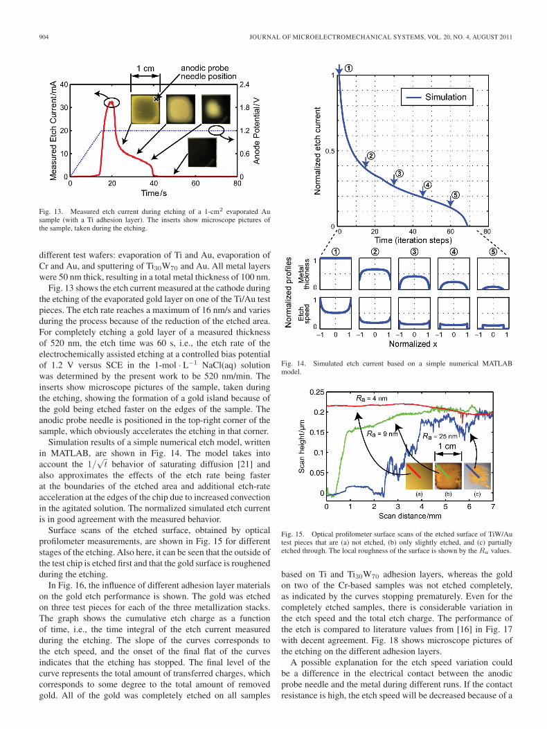
Fig. 13. Measured etch current during etching of a 1-cm2 evaporated Ausample (with a Ti adhesion layer). The inserts show microscope pictures ofthe sample, taken during the etching.
different test wafers: evaporation of Ti and Au, evaporation ofCr and Au, and sputtering of Ti30W70 and Au. All metal layerswere 50 nm thick, resulting in a total metal thickness of 100 nm.
Fig. 13 shows the etch current measured at the cathode duringthe etching of the evaporated gold layer on one of the Ti/Au testpieces. The etch rate reaches a maximum of 16 nm/s and variesduring the process because of the reduction of the etched area.For completely etching a gold layer of a measured thicknessof 520 nm, the etch time was 60 s, i.e., the etch rate of theelectrochemically assisted etching at a controlled bias potentialof 1.2 V versus SCE in the 1-mol · L−1 NaCl(aq) solutionwas determined by the present work to be 520 nm/min. Theinserts show microscope pictures of the sample, taken duringthe etching, showing the formation of a gold island because ofthe gold being etched faster on the edges of the sample. Theanodic probe needle is positioned in the top-right corner of thesample, which obviously accelerates the etching in that corner.
Simulation results of a simple numerical etch model, writtenin MATLAB, are shown in Fig. 14. The model takes intoaccount the 1/
√t behavior of saturating diffusion [21] and
also approximates the effects of the etch rate being fasterat the boundaries of the etched area and additional etch-rateacceleration at the edges of the chip due to increased convectionin the agitated solution. The normalized simulated etch currentis in good agreement with the measured behavior.
Surface scans of the etched surface, obtained by opticalprofilometer measurements, are shown in Fig. 15 for differentstages of the etching. Also here, it can be seen that the outside ofthe test chip is etched first and that the gold surface is roughenedduring the etching.
In Fig. 16, the influence of different adhesion layer materialson the gold etch performance is shown. The gold was etchedon three test pieces for each of the three metallization stacks.The graph shows the cumulative etch charge as a functionof time, i.e., the time integral of the etch current measuredduring the etching. The slope of the curves corresponds tothe etch speed, and the onset of the final flat of the curvesindicates that the etching has stopped. The final level of thecurve represents the total amount of transferred charges, whichcorresponds to some degree to the total amount of removedgold. All of the gold was completely etched on all samples
Fig. 14. Simulated etch current based on a simple numerical MATLABmodel.
Fig. 15. Optical profilometer surface scans of the etched surface of TiW/Autest pieces that are (a) not etched, (b) only slightly etched, and (c) partiallyetched through. The local roughness of the surface is shown by the Ra values.
based on Ti and Ti30W70 adhesion layers, whereas the goldon two of the Cr-based samples was not etched completely,as indicated by the curves stopping prematurely. Even for thecompletely etched samples, there is considerable variation inthe etch speed and the total etch charge. The performance ofthe etch is compared to literature values from [16] in Fig. 17with decent agreement. Fig. 18 shows microscope pictures ofthe etching on the different adhesion layers.
A possible explanation for the etch speed variation couldbe a difference in the electrical contact between the anodicprobe needle and the metal during different runs. If the contactresistance is high, the etch speed will be decreased because of a

STERNER et al.: ELECTROCHEMICALLY ASSISTED MASKLESS SELECTIVE REMOVAL OF METAL LAYERS 905
Fig. 16. Comparison of the etch performance of gold on different adhesionlayer materials. On all of the samples using Ti and TiW, the gold was etchedcompletely, whereas on most of the Cr samples, the gold etching stoppedprematurely.
Fig. 17. Current density as a function of electrode potential for the differenttest samples, compared to the data from [16].
Fig. 18. Microscope pictures taken during the etching of the gold on differentadhesion layer materials.
larger voltage drop. A source of error in measuring the totaletch charge could be the additional electrolysis of H2O intoH2 and O2, which theoretically occurs already at 1-V poten-tial difference to the reference electrode [22]. The prematurestopping of the etching on the samples with a Cr adhesion layeris explained by the electrochemical etching also attacking the
Fig. 19. SEM picture of an overhang test structure metallized by sputterdeposition of gold. Even though the metal is deposited from the top, there isa continuous layer deposited even in the inner part of the shadowed area. Thus,under these sputtering conditions, there will be a thin electrical bridge reducingthe selectivity between the gold areas when etched electrochemically.
Fig. 20. SEM picture of a stopper used to prevent short circuit between theswitch cantilever and the actuator electrode.
adhesion layer: Literature values for the anodic dissolution ofchromium in chloride solutions show that it is attacked at a rateof 10−2 A/cm2 which is comparable to that of gold at 1.2 V[16], [23], and thus, parts of the sample become completelyisolated from the anode and are not further etched. Ti andTiW have a much higher resistance to chloride corrosion: Thecurrent densities at 1.2 V are approximately 10−5 A/cm2 [24]and 10−4 A/cm2 [25], respectively, i.e., the selectivities of theselayers to gold are about 1 : 1000 and 1 : 100, respectively.
The etch selectivity to gold areas on the device layer whichare not electrically connected to the anode was determinedby measuring line scans of the surface profile of biased andunbiased samples, before and after etching, using an opticalprofilometer. No detectable etching of the unbiased samplecould be seen even after 1-h etching time (the total etching after1 h was smaller than the surface roughness of less than 3 nm).Furthermore, no detectable etching of unbiased gold areas inclose proximity to the biased areas, which were etched at520 nm/min, was seen on test samples featuring a 500-nm goldlayer on a 1-μm oxidized low-resistivity silicon substrate, inwhich 40-μm-wide and 125-μm-deep dicing lines were cut toisolate the neighboring areas for the purpose of measuring theetching selectivity.

906 JOURNAL OF MICROELECTROMECHANICAL SYSTEMS, VOL. 20, NO. 4, AUGUST 2011
Fig. 21. Selective removal of the gold coating from the stopper drastically reduces the stopper wear observed after 150 million switching cycles. The stoppertip with gold shows heavy contact wear, whereas there are no signs of wear on the stopper tip where the gold coating has been removed. The deformation ofthe gold on the sidewall of the moving cantilever, where the gold is not removed, can be clearly seen in both cases. (a) Gold-coated stopper and cantilever, after150 million actuation cycles. (b) Stopper with gold locally removed, after 150 million actuation cycles.
VI. CONSIDERATIONS ON THE STEP COVERAGE
OF THE METALLIZATION LAYERS
The SOI RF MEMS 3-D transmission line structure (seeFig. 1) requires a certain step coverage in the metallizationof the device layer in order to sufficiently cover the sidewallsof the transmission line. However, if the step coverage istoo high, a thin metallic interconnection between the devicelayer and the handle layer of the structures might short-circuitthese metal layers, which means that gold on the device layerwould also be etched when the gold on the handle layer iselectrochemically etched. This issue was observed on someof the chips where, while most isolated elements remainedunetched, some waveguide elements were visibly attacked andsome were completely etched. Fig. 19 shows a SEM picture ofa photoresist test structure with a 5-μm overhang, where eventhe most shadowed part is coated due to resputtering from thehandle substrate during the metal coating. Appropriate tuningof the deposition parameters avoids this problem, resulting inelectrically isolated areas as shown in Fig. 11.
VII. LOCAL REMOVAL OF GOLD ON INDIVIDUAL
DEVICE LAYER ELEMENTS
In addition to the removal of the gold on the handle layerof SOI RF MEMS devices, as demonstrated in the previoussections of this paper, the method can also be used to locallyremove gold from individual isolated elements in the devicelayer. This is shown in this section for removing gold onindividual stoppers (Fig. 20) of electrostatic actuators withoutisolation layers, reducing the wear between these nonelec-trically functioning mechanical contact points [8]. Repeatedactuation causes mechanical wear of the gold on the stopper
tips which increases the susceptibility of stiction and thusdrastically reduces lifetime.
The electrochemically assisted etching is applied to locallyremoving the gold on the stoppers. For the etching, the top goldsurface of the stoppers to be etched was directly contacted withthe anodic probe needle. To judge the effect on the mechanicalwear of the stopper tips, test devices with or without gold ontheir stoppers were actuated for 150 million cycles at 3-kHzswitching frequency. Even though stiction was not observed forany device for these low cycle numbers, a clear difference in thestopper tip wear was observed. Fig. 21(a) shows heavy contactwear of a gold-covered stopper tip, whereas Fig. 21(b) shows nosigns of wear after 150 million cycles for a stopper tip wherethe gold coating had been removed. A material analysis wasperformed using an Oxford INCA EDX system, showing thatthe gold had been removed from the stopper and its sidewalls.A comparison between unactuated and actuated stopper tipsindicated that some gold is transferred from the still gold-coatedcantilever side to the stopper tip during the 150 million cycles.
VIII. CONCLUSION
A novel method for selective local removal of metal layersusing maskless electrochemically assisted wet etching has beenpresented and successfully applied to the fabrication of 3-Dmicromachined SOI RF MEMS transmission lines with em-bedded laterally actuated microswitches. RF characterizationof the transmission lines shows good correspondence withsimulations and verifies the need for etching the metal layers.Furthermore, selective removal of the metallization on stoppershas been shown to drastically reduce the mechanical wear onthe stopper tip.

STERNER et al.: ELECTROCHEMICALLY ASSISTED MASKLESS SELECTIVE REMOVAL OF METAL LAYERS 907
REFERENCES
[1] M. Sterner, N. Roxhed, G. Stemme, and J. Oberhammer, “Masklessselective electrochemically assisted wet etching of metal layers for 3Dmicromachined SOI RF MEMS devices,” in Proc. IEEE Int. Conf. MEMS,Tucson, AZ, Jan. 2008, pp. 383–386.
[2] C. P. Wen, “Coplanar waveguide: A surface strip transmission line suit-able for nonreciprocal gyromagnetic device applications,” IEEE Trans.Microw. Theory Tech., vol. MMS-17, no. 12, pp. 1087–1090, Dec. 1969.
[3] I. Llamas-Garro and A. Corona-Chavez, “Micromachined transmissionlines for millimeter-wave applications,” in Proc. Int. Conf. CONIELE-COMP, Puebla, Mexico, Feb. 2006, p. 15.
[4] Y. Zhao, Y.-K. Yoon, X. Wu, and M. G. Allen, “Metal-transfer-micromolding of air-lifted RF components,” in Proc. TRANSDUCERS,Lyon, France, Jun. 2007, pp. 659–662.
[5] K. Herrick, T. Schwarz, and L. Katehi, “Si-micromachined coplanarwaveguides for use in high-frequency circuits,” IEEE Trans. Microw.Theory Tech., vol. 46, no. 6, pp. 762–768, Jun. 1998.
[6] A. Liu, M. Tang, A. Agarwal, and A. Alphones, “Low-loss lateral mi-cromachined switches for high frequency applications,” J. Micromech.Microeng., vol. 15, no. 1, pp. 157–167, Jan. 2005.
[7] J. Oberhammer, M. Tang, A.-Q. Liu, and G. Stemme, “Mechanically tri-stable, true single-pole-double-throw (SPDT) switches,” J. Micromech.Microeng., vol. 16, no. 11, pp. 2251–2258, Nov. 2006.
[8] M. Sterner, N. Roxhed, G. Stemme, and J. Oberhammer, “Static zero-power-consumption coplanar waveguide embedded DC-to-RF metal-contact MEMS switches in two-port and three-port configuration,” IEEETrans. Electron Devices, vol. 57, no. 7, pp. 1659–1669, Jul. 2010.
[9] M. Datta and D. Landolt, “Fundamental aspects and applications ofelectrochemical microfabrication,” Electrochim. Acta, vol. 45, no. 15/16,pp. 2535–2558, Jul. 2000.
[10] D. Landolt, “Electrodeposition science and technology in the last quarterof the twentieth century,” J. Electrochem. Soc., vol. 149, no. 3, pp. S9–S20, Apr. 2002.
[11] L. T. Romankiw, “A path: From electroplating through lithographic masksin electronics to LIGA in MEMS,” Electrochim. Acta, vol. 42, no. 20–22,pp. 2985–3005, 1997.
[12] A. Rogner, J. Eicher, D. Munchmeyer, R. P. Peters, and J. Mohr,“The LIGA technique—What are the new opportunities,” J. Micromech.Microeng., vol. 2, no. 3, pp. 133–140, Sep. 1992.
[13] W. J. McTegart, The Electrolytic and Chemical Polishing of Metals. Lon-don, U.K.: Pergamon, 1956.
[14] R. Schuster, V. Kirchner, P. Allongue, and G. Ertl, “Electrochemical mi-cromachining,” Science, vol. 289, no. 5476, pp. 98–101, Jul. 2000.
[15] A. C. West, C. Madore, M. Matlosz, and D. Landolt, “Shape changes dur-ing through-mask electrochemical micromachining of thin metal films,”J. Electrochem. Soc., vol. 139, no. 2, pp. 499–506, Feb. 1992.
[16] R. P. Frankenthal and D. J. Siconolfi, “The anodic corrosion of gold inconcentrated chloride solutions,” J. Electrochem. Soc., vol. 129, no. 6,pp. 1192–1196, Jun. 1982.
[17] S. Ye, C. Ishibashi, K. Shimazu, and K. Uosaki, “An in situ electro-chemical quartz crystal microbalance study of the dissolution processof a gold electrode in perchloric acid solution containing chloride ion,”J. Electrochem. Soc., vol. 145, no. 5, pp. 1614–1623, May 1998.
[18] Z. Hu and T. Ritzdorf, “Cyanide- and thiourea-free electrochemical etch-ing of gold for microelectronics applications,” J. Electrochem. Soc.,vol. 154, no. 10, pp. D543–D549, Aug. 2007.
[19] H. Gradin, S. Braun, G. Stemme, and W. van der Wijngaart, “Localizedremoval of the Au–Si eutectic bonding layer for the selective release ofmicrostructures,” J. Micromech. Microeng., vol. 19, no. 10, p. 105 014,Oct. 2009.
[20] J. T. Santini, Jr., A. C. Richards, R. Scheidt, M. J. Cima, and R. Langer,“Microchips as controlled drug-delivery devices,” Angew. Chem. Int. Ed.,vol. 39, no. 14, pp. 2396–2407, Jul. 2000.
[21] C. H. Hamann, A. Hamnett, and W. Vielstich, Electrochemistry, 2nd ed.Weinheim, Germany: Wiley-VCH, 2007.
[22] S. Licht, L. Halperin, M. Kalina, M. Zidman, and N. Halperin, “Electro-chemical potential tuned solar water splitting,” Chem. Commun., no. 24,pp. 3006–3007, Nov. 2003.
[23] N. D. Greene, C. R. Bishop, and M. Stern, “Corrosion and electrochemicalbehavior of chromium–noble metal alloys,” J. Electrochem. Soc., vol. 108,no. 9, pp. 836–841, Sep. 1961.
[24] S. Y. Yu and J. R. Scully, “Corrosion and passivity of Ti-13in comparisonto other biomedical implant alloys,” Corrosion, vol. 53, no. 12, pp. 965–976, Dec. 1997.
[25] J. Bhattarai, E. Akiyama, A. Kawashima, K. Asami, and K. Hashimoto,“The corrosion behavior of sputter-deposited amorphous W–Ti alloys in6 M HCl solution,” Corros. Sci., vol. 37, no. 12, pp. 2071–2086, Dec. 1995.
Mikael Sterner was born in Stockholm, Sweden,in 1981. He received the M.Sc. degree in engineer-ing physics from the Royal Institute of Technology(KTH), Stockholm, in 2006, where he has beenworking toward the Ph.D. degree in microsystemstechnology in the Microsystem Technology Labora-tory since 2006.
His main research fields include radio-frequencymicroelectromechanical systems (MEMS) switchesand microwave MEMS tunable high-impedancesurfaces.
Niclas Roxhed (M’09) was born in Stockholm,Sweden, in 1978. He received the M.Sc. degreein electrical engineering and the Ph.D. degree inmicrosystem technology from the Royal Institute ofTechnology (KTH), Stockholm, in 2003 and 2007,respectively.
He is currently an Assistant Professor at KTH,where he is leading research activities in medical-related microelectromechanical systems (MEMS).His main research fields include sensors for medicaldiagnostics and medical-aid microsystems. He is also
involved in high-precision etching using deep reactive ion etching for radio-frequency MEMS switches and 3-D integration of MEMS on ICs for infraredimagers. He has authored or coauthored 39 scientific papers.
Göran Stemme (M’98–SM’04–F’06) received theM.Sc. degree in electrical engineering and the Ph.D.degree in solid-state electronics from Chalmers Uni-versity of Technology, Gothenburg, Sweden, in 1981and 1987, respectively.
In 1981, he was with the Department of SolidState Electronics, Chalmers University of Technol-ogy, where he was an Associate Professor (docent)heading the silicon sensor research group in 1990.Since 1991, he has been a Professor at the RoyalInstitute of Technology (KTH), Stockholm, Sweden,
where he is the Head of the Microsystem Technology Lab in the School ofElectrical Engineering. His research is devoted to microsystem technologybased on micromachining of silicon. The work spans a broad range of tech-nological and application fields, such as medical technology, biochemistry,biotechnology, microfluidics, optical applications, wafer-level packaging, anddevice integration. Some of the results have successfully been commercialized.He has published more than 260 research journal and conference papers andis the holder of more than 22 patent proposals or granted patents. He was amember of the Editorial Board of the Royal Society of Chemistry journal Labon a Chip between 2000 and 2005.
Dr. Stemme is a member of the Royal Swedish Academy of Sciences (KVA).Between 1995 and 2001, he was a member of the International Steering Com-mittee of the IEEE Micro Electro Mechanical Systems Conference series, andhe was the General Cochair of that conference in 1998. He has been a memberof the Editorial Board of the JOURNAL OF MICROELECTROMECHANICAL
SYSTEMS since 1997. In 2001, he won, together with two colleagues, the finalof the Innovation Cup in Sweden.

908 JOURNAL OF MICROELECTROMECHANICAL SYSTEMS, VOL. 20, NO. 4, AUGUST 2011
Joachim Oberhammer (M’06) was born in Italyin 1976. He received the M.Sc. degree in elec-trical engineering from Graz University of Tech-nology, Graz, Austria, in 2000, and the Ph.D.degree from the Royal Institute of Technology(KTH), Stockholm, Sweden, in 2004, for his work onradio-frequency (RF) microelectromechanical sys-tems (MEMS) switches and microsystem packaging.
He was working with automotive sensor electron-ics and RF identification systems at Graz Universityof Technology and Vienna University of Technology,
Vienna, Austria, before he joined the Microsystem Technology Laboratory,KTH. He was a Postdoctoral Research Fellow at Nanyang TechnologicalUniversity, Singapore. Since 2005, he has been with KTH, where he was anAssistant Professor, has been an Associate Professor since 2007, and is headinga research team with activities in RF and microwave MEMS. In 2007, he wasa Research Consultant at Nanyang Technological University. In 2008, he wasa Guest Researcher at Kyoto University, Kyoto, Japan, where he spent sevenmonths. He is the author or coauthor of more than 60 reviewed research papersand is the holder of four patents.
Dr. Oberhammer has been a Steering Group member of the IEEE MicrowaveTheory and Techniques Society (MTT-S) and IEEE Antennas and PropagationSociety (AP-S) Chapters in Sweden since 2009. He was a recipient of theEricsson Research Foundation Award in 2004, a grant by the Swedish Inno-vation Bridge in 2007, and a visiting researcher scholarship from the JapaneseSociety for the Promotion of Science in 2008. The research work he is headingreceived the Best Paper Award at the IEEE European Microwave IntegratedCircuit Conference in 2009, the Best Student Paper Award at the IEEE Asia-Pacific Microwave Conference in 2010, and Graduate Fellowships from theIEEE MTT-S in 2010 and in 2011. He served as a TPRC member of IEEETransducers 2009, IEEE International Microwave Symposium 2010 and 2011,and IEEE Micro Electro Mechanical Systems 2011.