Electro-Optical Characterization Team (Presentation) · PDF fileElectro-Optical...
18
DOE Solar Energy Technologies Program Peer Review Denver, Colorado April 17, 2007 Electro Electro - - Optical Characterization Team Optical Characterization Team NREL NREL Dean Levi Dean Levi
-
Upload
vuonghuong -
Category
Documents
-
view
219 -
download
3
Transcript of Electro-Optical Characterization Team (Presentation) · PDF fileElectro-Optical...
DOE Solar Energy Technologies Program Peer Review
Denver, Colorado April 17, 2007
ElectroElectro--Optical Characterization TeamOptical Characterization Team
NRELNREL
Dean LeviDean Levi
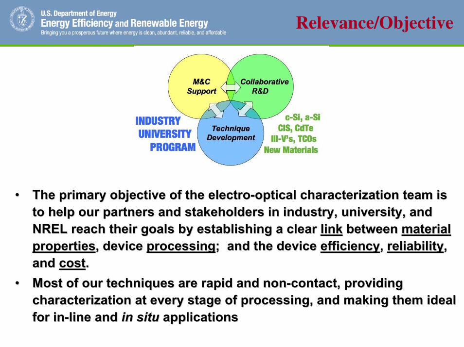
Relevance/Objective
•• The primary objective of the electroThe primary objective of the electro--optical characterization team is optical characterization team is to help our partners and stakeholders in industry, university, ato help our partners and stakeholders in industry, university, and nd NREL reach their goals by establishing a clear NREL reach their goals by establishing a clear linklink between between material material propertiesproperties, device , device processingprocessing; and the device ; and the device efficiencyefficiency, , reliabilityreliability, , and and costcost..
•• Most of our techniques are rapid and nonMost of our techniques are rapid and non--contact, providing contact, providing characterization at every stage of processing, and making them icharacterization at every stage of processing, and making them ideal deal for infor in--line and line and in situin situ applicationsapplications
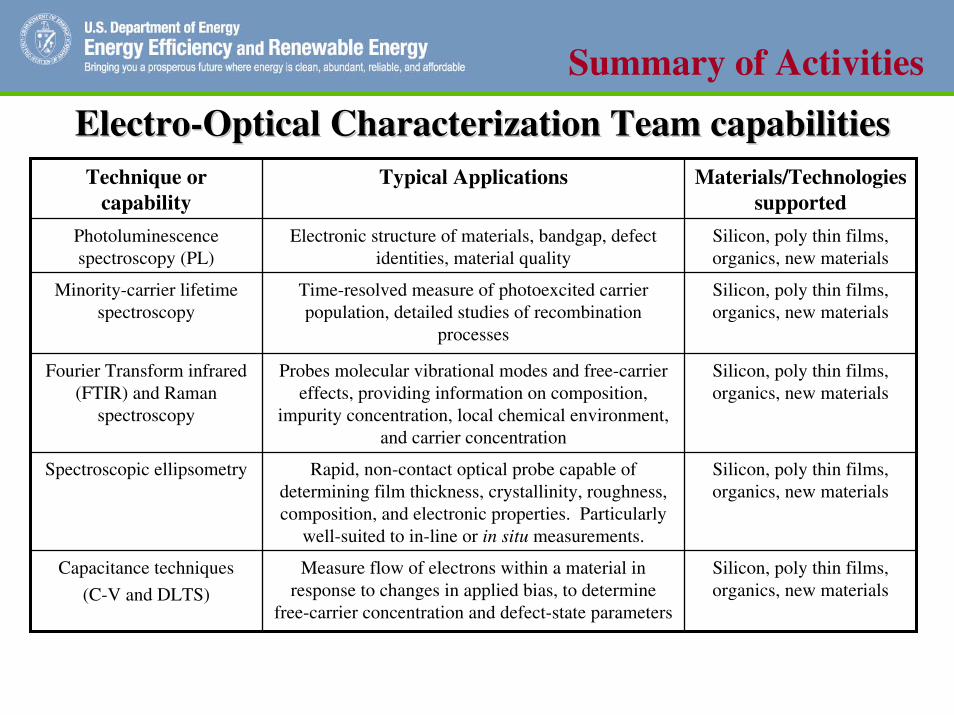
Summary of Activities
ElectroElectro--Optical Characterization Team capabilitiesOptical Characterization Team capabilitiesTechnique or
capabilityTypical Applications Materials/Technologies
supported
Photoluminescence spectroscopy (PL)
Electronic structure of materials, bandgap, defect identities, material quality
Silicon, poly thin films, organics, new materials
Minority-carrier lifetime spectroscopy
Time-resolved measure of photoexcited carrier population, detailed studies of recombination
processes
Silicon, poly thin films, organics, new materials
Fourier Transform infrared (FTIR) and Raman
spectroscopy
Probes molecular vibrational modes and free-carrier effects, providing information on composition,
impurity concentration, local chemical environment, and carrier concentration
Silicon, poly thin films, organics, new materials
Spectroscopic ellipsometry Rapid, non-contact optical probe capable of determining film thickness, crystallinity, roughness, composition, and electronic properties. Particularly
well-suited to in-line or in situ measurements.
Silicon, poly thin films, organics, new materials
Capacitance techniques
(C-V and DLTS)
Measure flow of electrons within a material in response to changes in applied bias, to determine
free-carrier concentration and defect-state parameters
Silicon, poly thin films, organics, new materials
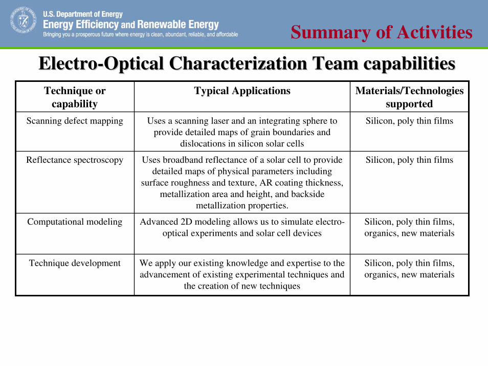
Summary of Activities
ElectroElectro--Optical Characterization Team capabilitiesOptical Characterization Team capabilitiesTechnique or
capabilityTypical Applications Materials/Technologies
supported
Scanning defect mapping Uses a scanning laser and an integrating sphere to provide detailed maps of grain boundaries and
dislocations in silicon solar cells
Silicon, poly thin films
Reflectance spectroscopy Uses broadband reflectance of a solar cell to provide detailed maps of physical parameters including
surface roughness and texture, AR coating thickness, metallization area and height, and backside
metallization properties.
Silicon, poly thin films
Computational modeling Advanced 2D modeling allows us to simulate electro-optical experiments and solar cell devices
Silicon, poly thin films, organics, new materials
Technique development We apply our existing knowledge and expertise to the advancement of existing experimental techniques and
the creation of new techniques
Silicon, poly thin films, organics, new materials
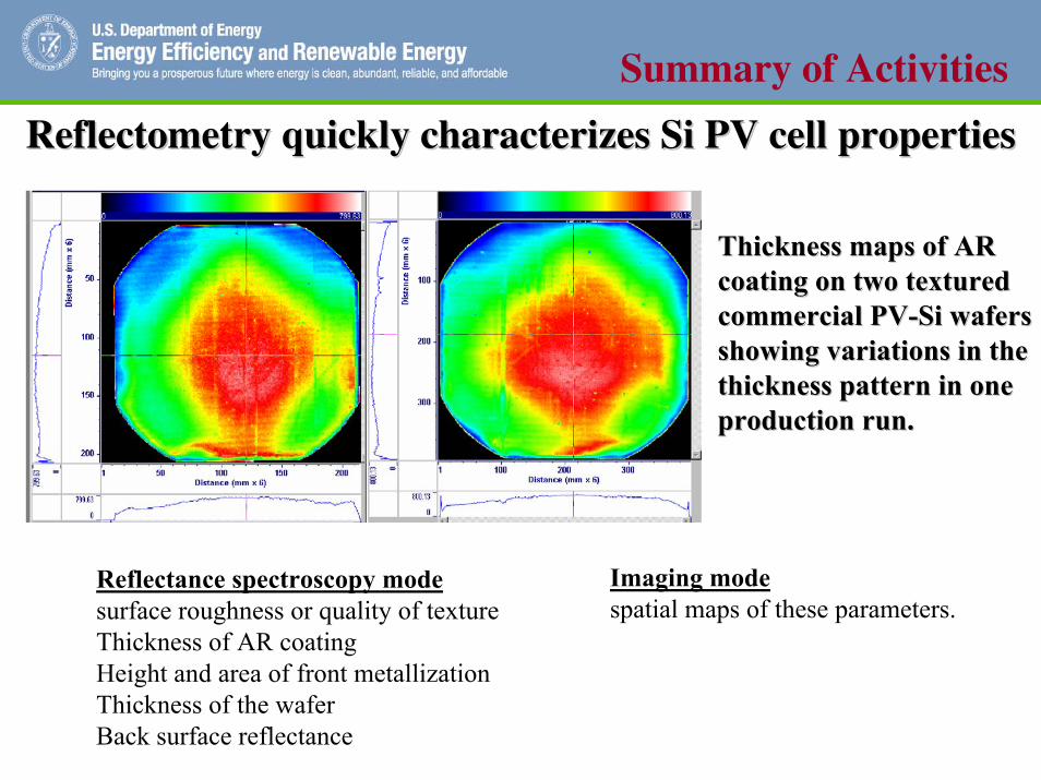
Summary of Activities
Reflectometry quickly characterizes Si PV cell propertiesReflectometry quickly characterizes Si PV cell properties
Thickness maps of AR Thickness maps of AR coating on two textured coating on two textured commercial PVcommercial PV--Si wafers Si wafers showing variations in the showing variations in the thickness pattern in one thickness pattern in one production run.production run.
Reflectance spectroscopy modesurface roughness or quality of textureThickness of AR coatingHeight and area of front metallizationThickness of the waferBack surface reflectance
Imaging modespatial maps of these parameters.
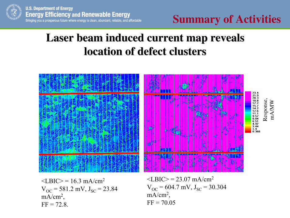
Summary of Activities
Laser beam induced current map reveals Laser beam induced current map reveals location of defect clusterslocation of defect clusters
<LBIC> = 16.3 mA/cm2
VOC = 581.2 mV, JSC = 23.84 mA/cm2, FF = 72.8.
<LBIC> = 23.07 mA/cm2
VOC = 604.7 mV, JSC = 30.304 mA/cm2, FF = 70.05
Res
pons
e,
mA
/MW
Summary of Activities
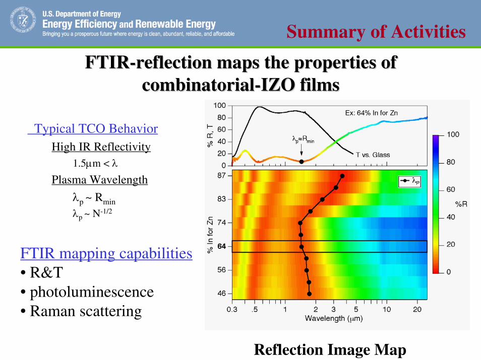
FTIRFTIR--reflection maps the properties of reflection maps the properties of combinatorialcombinatorial--IZO filmsIZO films
Typical TCO BehaviorHigh IR Reflectivity
1.5μm < λ
Plasma Wavelength
λp ~ Rmin
λp ~ N-1/2
Reflection Image Map
FTIR mapping capabilities• R&T• photoluminescence• Raman scattering
Summary of Activities
Multiple techniques are being developed for Si material Multiple techniques are being developed for Si material quality evaluation using carrier lifetime measurementsquality evaluation using carrier lifetime measurements
•• Our group has pioneered development of photoconductive decay Our group has pioneered development of photoconductive decay techniques (RCPCD) for characterization of photoexcited carrier techniques (RCPCD) for characterization of photoexcited carrier lifetime lifetime and material quality in cand material quality in c--Si and Si and pxpx--Si for PV.Si for PV.
•• We have recently developed and tested 1We have recently developed and tested 1--D and 2D and 2--D mapping of lifetime D mapping of lifetime using RCPCD.using RCPCD.
•• We are currently studying the relationship between PL intensitWe are currently studying the relationship between PL intensity and y and lifetime for PL lifetime mapping in Si wafers.lifetime for PL lifetime mapping in Si wafers.
•• We are examining the accuracy of microwave reflectivity lifetiWe are examining the accuracy of microwave reflectivity lifetime me measurements, as well as pumpmeasurements, as well as pump--probe freeprobe free--carrier absorption techniquescarrier absorption techniques
•• NREL researchNREL research--fellow emeritus Richard Ahrenkiel recently completed a 6 fellow emeritus Richard Ahrenkiel recently completed a 6 month study of lifetime measurement needs of the Si PV industry,month study of lifetime measurement needs of the Si PV industry, which will which will guide our technique development work in this area.guide our technique development work in this area.
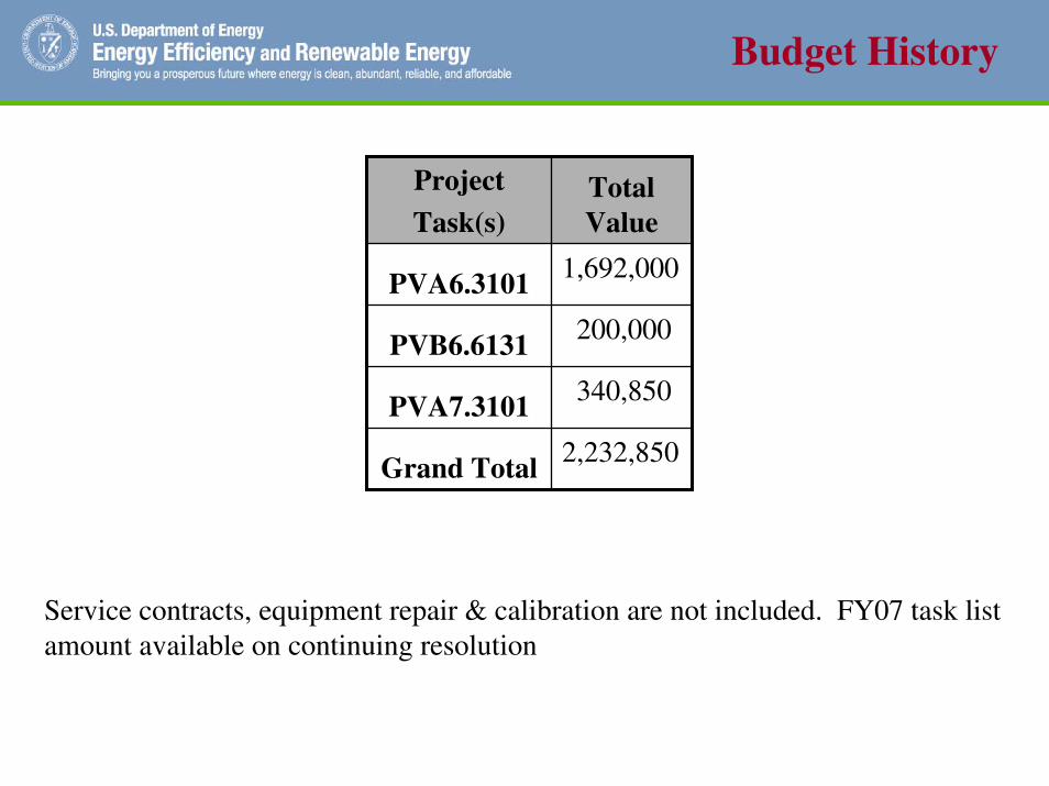
Budget History
Project
Task(s)Total Value
PVA6.3101
PVB6.6131
PVA7.3101
Grand Total
1,692,000
200,000
340,850
2,232,850
Service contracts, equipment repair & calibration are not included. FY07 task list amount available on continuing resolution
Accomplishments
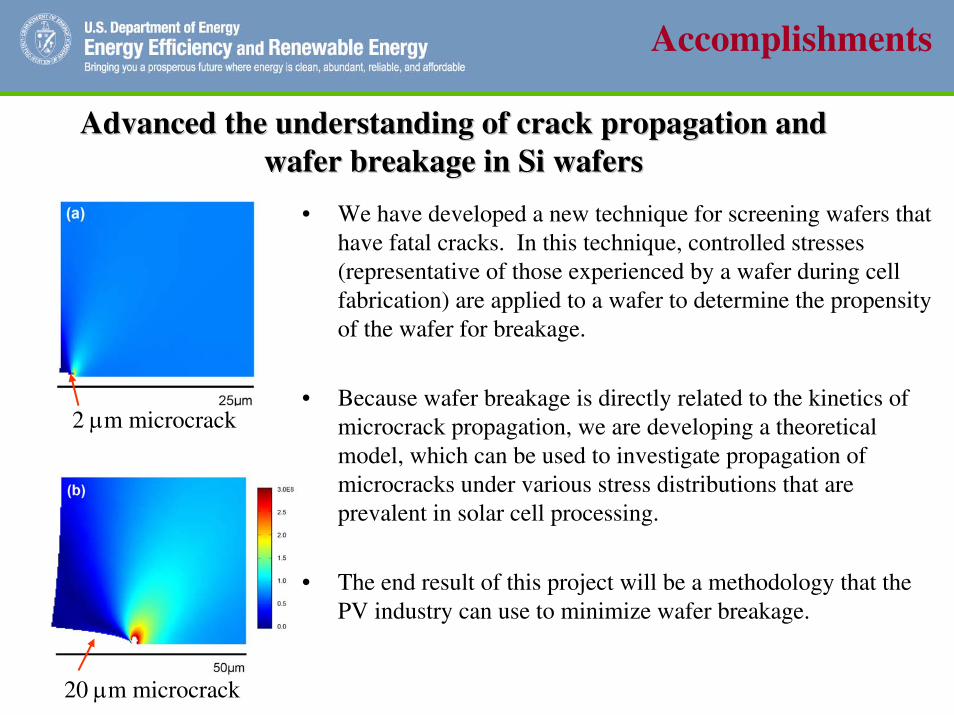
Advanced the understanding of crack propagation and Advanced the understanding of crack propagation and wafer breakage in Si waferswafer breakage in Si wafers
• We have developed a new technique for screening wafers that have fatal cracks. In this technique, controlled stresses (representative of those experienced by a wafer during cell fabrication) are applied to a wafer to determine the propensity of the wafer for breakage.
• Because wafer breakage is directly related to the kinetics of microcrack propagation, we are developing a theoretical model, which can be used to investigate propagation of microcracks under various stress distributions that are prevalent in solar cell processing.
• The end result of this project will be a methodology that the PV industry can use to minimize wafer breakage.
2 μm microcrack
20 μm microcrack
Accomplishments
Metallization Firing and Metallization Firing and SiN:HSiN:H Studies Studies (in collaboration with BP Solar, Ferro, and Applied Materials).
– We have built an optical processing furnace with a capability to exhaust effluent, monitor the temperature distribution of the entire solar cell using multiple thermocouples attached to the cell itself, and control the entire process cycle.
– Two important findings are:
• For a given optical flux, screen-printed cells exhibit a large temperature difference between regions with and without front metallization. (812 °C, away from the buss bar, 786 °C under the buss-bar)
• These temperatures are far below the eutectic point of Ag-Si (835oC) and the melting point of Ag (961.9oC), yet they yield low-resistance ohmic contacts.
Accomplishments
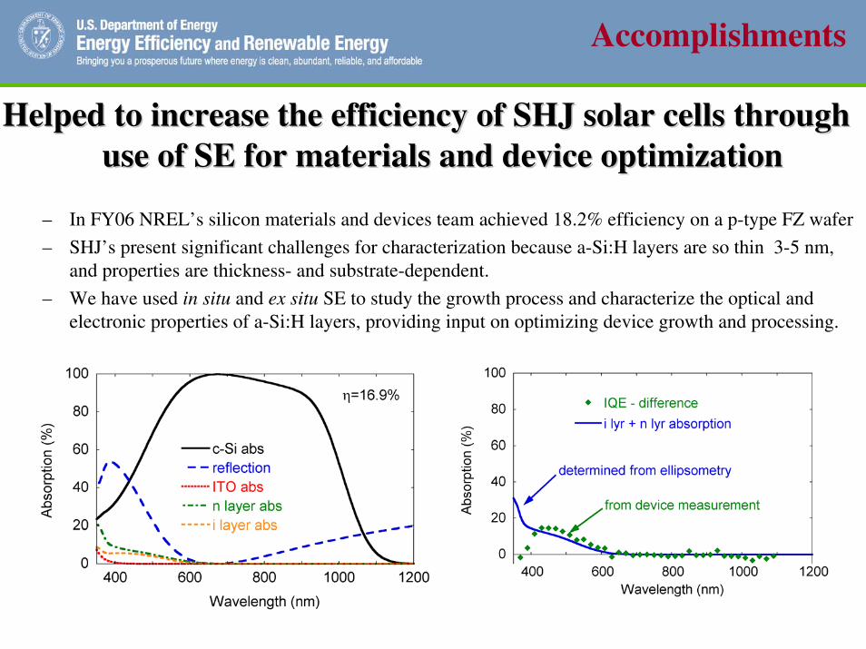
Helped to increase the efficiency of SHJ solar cells through Helped to increase the efficiency of SHJ solar cells through use of SE for materials and device optimizationuse of SE for materials and device optimization
– In FY06 NREL’s silicon materials and devices team achieved 18.2% efficiency on a p-type FZ wafer
– SHJ’s present significant challenges for characterization because a-Si:H layers are so thin 3-5 nm, and properties are thickness- and substrate-dependent.
– We have used in situ and ex situ SE to study the growth process and characterize the optical andelectronic properties of a-Si:H layers, providing input on optimizing device growth and processing.
Accomplishments
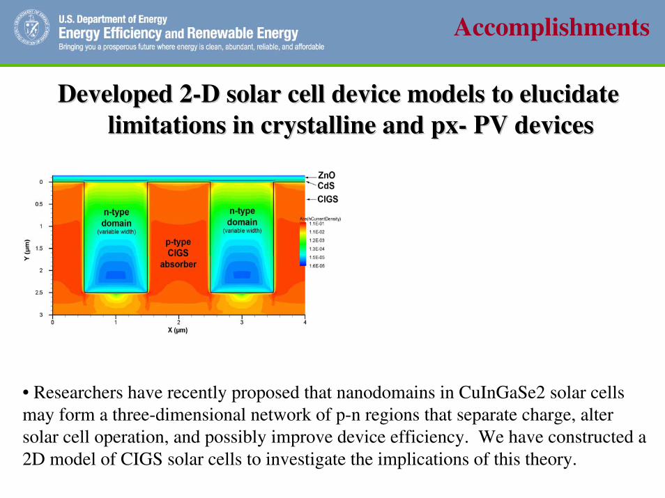
Developed 2Developed 2--D solar cell device models to elucidate D solar cell device models to elucidate limitations in crystalline and limitations in crystalline and pxpx-- PV devicesPV devices
• Researchers have recently proposed that nanodomains in CuInGaSe2 solar cells may form a three-dimensional network of p-n regions that separate charge, alter solar cell operation, and possibly improve device efficiency. We have constructed a 2D model of CIGS solar cells to investigate the implications of this theory.
Accomplishments
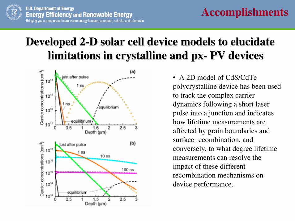
Developed 2Developed 2--D solar cell device models to elucidate D solar cell device models to elucidate limitations in crystalline and limitations in crystalline and pxpx-- PV devicesPV devices
• A 2D model of CdS/CdTe polycrystalline device has been used to track the complex carrier dynamics following a short laser pulse into a junction and indicates how lifetime measurements are affected by grain boundaries and surface recombination, and conversely, to what degree lifetime measurements can resolve the impact of these different recombination mechanisms on device performance.
Accomplishments
Organized the 16th Workshop on Crystalline Silicon Solar Organized the 16th Workshop on Crystalline Silicon Solar Cell & Modules: Materials and ProcessesCell & Modules: Materials and Processes
– The Silicon Workshop helps the Si-PV industry by (1) bringing together the industry, research, andacademic communities, (2) disseminating scientific and technical information, and (3) providing feedback to NREL/DOE on important research tasks, as perceived by the PV community.
– The workshop was attended by 157 scientists and engineers from 39 research institutions, DOE GO and HQ offices, and 34 international PV and semiconductor companies.
– This year’s sessions reviewed recent advances in crystal growth technologies, impurities and defects in semiconductors, feedstock issues, solar cell processing, thin-film Si and heterojunction devices, solar cell metallization, and module reliability issues. The theme of the workshop—“Getting More (Watts) for Less ($i)”—reflected the growing need for maximizing the use of silicon to obtain the largest amount of PV energy.
Schedule of Major Events/Milestones
•• 4/07 4/07 –– Develop and implement a plan to support the TPP awardees Develop and implement a plan to support the TPP awardees that can be met with available resources.that can be met with available resources.
•• 9/07 9/07 –– Organize the 17Organize the 17thth Workshop on Crystalline Silicon Solar Cell Workshop on Crystalline Silicon Solar Cell Materials and Processes; identify priority R&D issues for the SiMaterials and Processes; identify priority R&D issues for the Si PV PV industryindustry
•• 9/07 9/07 –– Establish a multiEstablish a multi--dimensional computer model for mcdimensional computer model for mc--Si Si devices; assess value and limitation of model output.devices; assess value and limitation of model output.
•• 9/07 9/07 –– Complete the study of the kinetics of microComplete the study of the kinetics of micro--crack propagation crack propagation and improve our understanding of how thermal profiling and and improve our understanding of how thermal profiling and mechanical stresses, associated with conventional processing, immechanical stresses, associated with conventional processing, impact pact propagation.propagation.
•• 9/07 9/07 –– Assess the technical shortcomings of minorityAssess the technical shortcomings of minority--carrier lifetime carrier lifetime measurement techniques used to determine material quality of mcmeasurement techniques used to determine material quality of mc--Si; apply improved understanding to facilitate better measuremenSi; apply improved understanding to facilitate better measurements ts of material quality for the PV industry; publish internal reportof material quality for the PV industry; publish internal report..
•• 9/07 9/07 –– Develop an Develop an in situin situ spectroscopic ellipsometry measurement spectroscopic ellipsometry measurement and analysis capability for the TCO sputtering tool in the PDIL.and analysis capability for the TCO sputtering tool in the PDIL.
Future Directions
•• Establish onEstablish on--going collaborative R&D relationships with SAI going collaborative R&D relationships with SAI TPP partners.TPP partners.–– Working together is much more effective than Working together is much more effective than ‘‘sample in, sample outsample in, sample out’’
•• Develop advanced multiDevelop advanced multi--dimensional models for 1dimensional models for 1stst, 2, 2ndnd, and , and 33rdrd generation PV technologiesgeneration PV technologies
•• Develop new measurement and characterization techniques Develop new measurement and characterization techniques in response to needs of the PV industry.in response to needs of the PV industry.–– ElectroElectro--optical techniques are welloptical techniques are well--suited for insuited for in--line and line and in situin situ
•• Advance the science and understanding of lifetime Advance the science and understanding of lifetime measurement techniques for Si PV applicationsmeasurement techniques for Si PV applications
•• Develop Develop in situin situ and inand in--line applications of spectroscopic line applications of spectroscopic ellipsometryellipsometry

Thank you for your attentionThank you for your attention