Electrical Transport and Channel Length Modulation in ... · influence electrical transport in FET...
23
AEROSPACE REPORT NO. ATR-2013-01138 Electrical Transport and Channel Length Modulation in Semiconducting Carbon Nanotube Field-Effect Transistors November 25, 2013 Adam W. Bushmaker Electronics and Photonics Laboratory Physical Sciences Laboratories Prepared for: Vice President Technology and Laboratory Operations Authorized by: Engineering and Technology Group PUELIC RELEASE IS AUTHORIZED Assuring Space Mission Success
Transcript of Electrical Transport and Channel Length Modulation in ... · influence electrical transport in FET...

AEROSPACE REPORT NO. ATR-2013-01138
Electrical Transport and Channel Length Modulation in Semiconducting Carbon Nanotube Field-Effect Transistors
November 25, 2013
Adam W. Bushmaker Electronics and Photonics Laboratory Physical Sciences Laboratories
Prepared for:
Vice President Technology and Laboratory Operations
Authorized by: Engineering and Technology Group
PUELIC RELEASE IS AUTHORIZED
Assuring Space Mission Success

PHYSICAL SCIENCES LABORATORIES
The Aerospace Corporation functions as an "architect-engineer" for national security programs, specializing in advanced military space systems. The Corporation's Physical Sciences Laboratories support the effective and timely development and operation of national security systems through scientific research and the application of advanced technology. Vital to the success of the Corporation is the technical staffs wide-ranging expertise and its ability to stay abreast of new technological developments and program support issues associated with rapidly evolving space systems. Contributing capabilities are provided by these individual organizations:
Electronics and Photonics Laboratory: Microelectronics, VLSI reliability, failure analysis, solid-state device physics, compound semiconductors, radiation effects, infrared and CCD detector devices, data storage and display technologies; lasers and electro-optics, solid-state laser design, micro-optics, optical communications, and fiber- optic sensors; atomic frequency standards, applied laser spectroscopy, laser chemistry, atmospheric propagation and beam control, L1DAR/LADAR remote sensing; solar cell and array testing and evaluation, battery electrochemistry, battery testing and evaluation.
Space Materials Laboratory: Evaluation and characterizations of new materials and processing techniques: metals, alloys, ceramics, polymers, thin films, and composites; development of advanced deposition processes; nondestructive evaluation, component failure analysis and reliability; structural mechanics, fracture mechanics, and stress corrosion; analysis and evaluation of materials at cryogenic and elevated temperatures; launch vehicle fluid mechanics, heat transfer and flight dynamics; aerothermodynamics; chemical and electric propulsion; environmental chemistry; combustion processes; space environment effects on materials, hardening and vulnerability assessment; contamination, thermal and structural control; lubrication and surface phenomena. Microelectromechanical systems (MEMS) for space applications; laser micromachining; laser-surface physical and chemical interactions; micropropulsion; micro- and nanosatellite mission analysis; intelligent microinstruments for monitoring space and launch system environments.
Space Science Applications Laboratory: Magnetospheric, auroral and cosmic-ray physics, wave-particle interactions, magnetospheric plasma waves; atmospheric and ionospheric physics, density and composition of the upper atmosphere, remote sensing using atmospheric radiation; solar physics, infrared astronomy, infrared signature analysis; infrared surveillance, imaging and remote sensing; multispectral and hyperspectral sensor development; data analysis and algorithm development; applications of multispectral and hyperspectral imagery to defense, civil space, commercial, and environmental missions; effects of solar activity, magnetic storms and nuclear explosions on the Earth's atmosphere, ionosphere and magnetosphere; effects of electromagnetic and particulate radiations on space systems; space instrumenta:ion, design, fabrication and test; environmental chemistry, trace detection; atmospheric chemical reactions, atmospheric optics, light scattering, state-specific chemical reactions, and radiative signatures of missile plumes.

AEROSPACE REPORT NO. ATR-2013-01138
Electrical Transport and Channel Length Modulation in Semiconducting Carbon Nanotube Field-Effect Transistors
November 25, 2013
Adam W. Bushmaker Electronics and Photonics Laboratory Physical Sciences Laboratories
Prepared for:
Vice President Technology and Laboratory Operations
Authorized by: Engineering and Technology Group
^/SO^GTO
PUBLIC RELEASE IS AUTHORIZED
(2) AEROSPACE ^—^ Assuring Space Mission Success
AEROSPACE REPORT NO. ATR-2013-01138
Electrical Transport and Channel Length Modulation in Semiconducting Carbon Nanotube Field-Effect Transistors
Approved by:
U^ g jj t^yt
Steven C. Moss, Director Microelectronics Technology Department Electronics and Photonics Laboratory Physical Sciences Laboratories
Walter F. Bdill^rincipal'Director Electronics and Photonics Laboratory Physical Sciences Laboratories
Terence S. Yeoh R&D Portfolio Manager Research & Program Development Office Engineering & Technology Group
© The Aerospace Corporation, 2013.
All trademarks, service marks, and trade names are the property of their respective owners.
80-2333(5632, 21, JS)
II

Abstract
We perform finite-element analysis modeling and characterization of quasi-ballistic electrical transport in semiconducting carbon nanotube field-effect transistors, and fit experimental electrical transport data from both suspended and on-substrate single- walled carbon nanotube transistors fabricated using chemical vapor deposition. Pre- vious studies have focused on modeling ballistic transport in carbon nanotube field- effect transistors, but have ignored the spatial dependence of the resistance, voltage, and Fermi energy. These spatial variations play an important role in several high- voltage effects that are particularly important in the quasi-ballistic transport regime where most current or near-term devices operate. We show the relationship between device geometry and pinch-off, current saturation, and channel length modulation in the quantum capacitance regime. Output resistance is found to increase with gate coupling efficiency with a power law behavior. This model can be used for extraction of device properties from experimental data and as a design environment tool.
111

Acknowledgments
The authors acknowledge Dr. George C. Valley of The Aerospace Corporation for discussions on computational stability.
IV
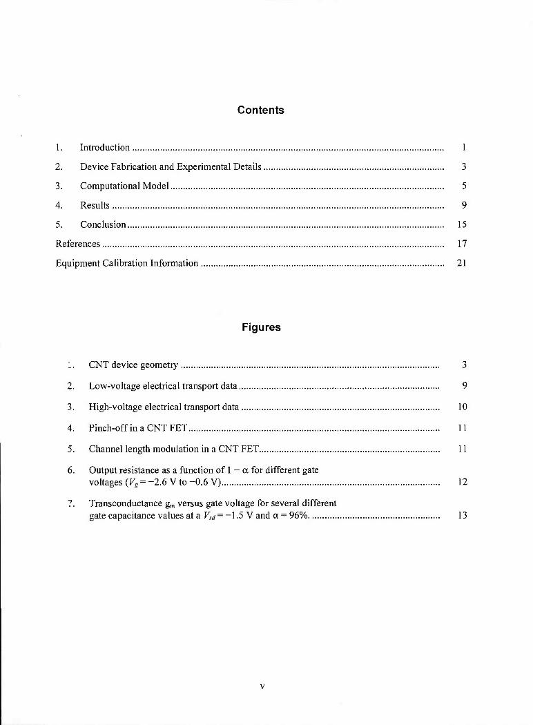
Contents
1. Introduction 1
2. Device Fabrication and Experimental Details 3
3. Computational Model 5
4. Results 9
5. Conclusion 15
References 17
Equipment Calibration Information 21
i
Figures
CNT device geometry 3
Low-voltage electrical transport data 9
3. High-voltage electrical transport data 10
4. Pinch-off in a CNT FET 11
5. Channel length modulation in a CNT FET 11
6. Output resistance as a function of 1 - a for different gate voltages (Fg =-2.6 V to-0.6 V) 12
T Transconductance gm versus gate voltage for several different gate capacitance values at a 1^= -1.5 V and a = 96% 13
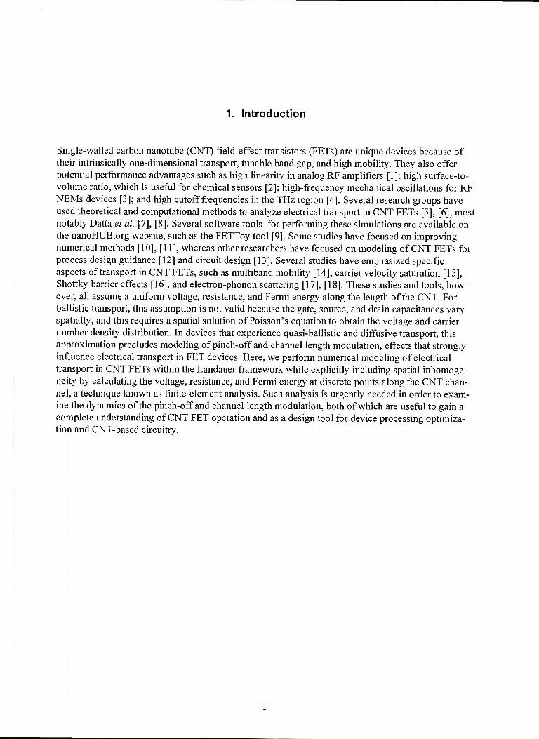
1. Introduction
Single-walled carbon nanotube (CNT) field-effect transistors (FETs) are unique devices because of their intrinsically one-dimensional transport, tunable band gap, and high mobility. They also offer potential performance advantages such as high linearity in analog RF amplifiers [1]; high surface-to- volume ratio, which is useful for chemical sensors [2]; high-frequency mechanical oscillations for RF NEMs devices [3]; and high cutoff frequencies in the THz region [4]. Several research groups have used theoretical and computational methods to analyze electrical transport in CNT FETs [5], [6], most notably Datta et al. [7], [8]. Several software tools for performing these simulations are available on the nanoFTUB.org website, such as the FETToy tool [9]. Some studies have focused on improving numerical methods [10], [11], whereas other researchers have focused on modeling of CNT FETs for process design guidance [12] and circuit design [13]. Several studies have emphasized specific aspects of transport in CNT FETs, such as multiband mobility [14], carrier velocity saturation [15], Shottky barrier effects [16], and electron-phonon scattering [17], [18]. These studies and tools, how- ever, all assume a uniform voltage, resistance, and Fermi energy along the length of the CNT. For ballistic transport, this assumption is not valid because the gate, source, and drain capacitances vary spatially, and this requires a spatial solution of Poisson's equation to obtain the voltage and carrier number density distribution. In devices that experience quasi-ballistic and diffusive transport, this approximation precludes modeling of pinch-off and channel length modulation, effects that strongly influence electrical transport in FET devices. Here, we perform numerical modeling of electrical transport in CNT FETs within the Landauer framework while explicitly including spatial inhomoge- neity by calculating the voltage, resistance, and Fermi energy at discrete points along the CNT chan- nel, a technique known as finite-element analysis. Such analysis is urgently needed in order to exam- ine the dynamics of the pinch-off and channel length modulation, both of which are useful to gain a complete understanding of CNT FET operation and as a design tool for device processing optimiza- tion and CNT-based circuitry.

2. Device Fabrication and Experimental Details
In order to validate the results from the model outlined in the body of this report, experimental data from suspended CNT FETs fabricated using chemical vapor deposition (CVD) are compared with output from the model. These samples are fabricated as reported previously [19], [20] on pre-defined platinum/tungsten electrode structures. Figure 1 shows scanning electron micrograph (SEM) images of a CNT FET device fabricated using this method. The CNT is grown in the CVD process across a trench etched in the underlying substrate, making electrical contact on both sides of the trench. The trench has a metallic top layer that serves as a gate electrode, with the ambient gas or vacuum serving as the dielectric between the CNT and the gate. The yield is low (-5%), and devices with CNTs suc- cessfully spanning the trench are selected for further study. The CVD process is the last step in fabri- cation, ensuring low defect concentration in the resulting CNT channel material.
Figure 1. CNT device geometry, (a) SEM images of CNT device layout and (b) close-up image of a single CNT crossing the trench.

3. Computational Model
In the Landauer model, electrical current flowing in a ballistic one-dimensional conductor is
/ = £>(£) ■ VgiE)[fR(E) - fdEME , (1)
where Vg(E) is the group velocity, D(E) is the density of states, and fR and fL are the quasi-Fermi functions for the right- and left-moving electron populations. From this equation, the resistance Rs of a diffusive CNT section "5" of length L can be approximated [14, 21] as
K' = KoVW(lOp^)dF, (2)
where R0 = ft/4e2 is the quantum resistance, A is the mean free path, / is the Fermi function for the av3rage Fermi energy EF = {EF R + Epjj/2 and the integral is taken over all energies except the
band gap, i.e., jbands dE = J^ dE + J£ dE. For multiple sections of one-dimensional conductor in
series with one another, the resistance can be calculated as
R= Ro + j:Rs + 2Rc, (3)
where
is :he depleted quantum resistance evaluated at the point of minimum doping on the CNT, and Rc is the contact resistance. If A » L (ballistic transport), the right-hand side of (3) reduces to the depleted quantum resistance plus the contact resistances. The mean free path A is, is given by
^ = (1/A +1/A T' (5)
where Aac, the mean free path for electron scattering by acoustic phonons, is given by
^E)=AhjhE{^.)2, (6)
where Aalf is the mean free path at high energies away from the band edge, and vF is the carrier
velocity in graphene. Acoustic scattering is approximated as elastic as in [14]. A more complete

discussion of electrical transport modeling with inelastic scattering accounted for can be found else- where [22]. The mean free path is related to the scattering rate T
_1(£') according to Aac(E) - T(E) *
Vg{E). Because the scattering rate increases with the density of states (Fermi's golden rule) near the band edge, T
-1^) a D{E) « u5
_1(E). A full derivation of this effect is beyond the scope of this report, but the divergence of the scattering rate at the band edge where the group velocity goes to zero can be seen elsewhere in the carbon nanotube literature [23-25]. The combined effect gives a mean free path proportionate to Vg. The energy dependence of Aac is thermally averaged, but still varies by a factor of 5 or so at room temperature as the Fermi energy is changed. Electrons in one-dimensional systems scatter strongly from with K-point optical phonons [26]. The mean free path with respect to electron scattering through optical phonon emission A0p ems is given by
*-op,ems ~ y r ^■op.m.in » (')
where V is the voltage drop across the segment, h0VTnin is the scattering length for electrons with enough energy to emit an optical phonon, and Eov = 0.16eV is the optical phonon energy of the zone- boundary optical phonons [26]. The voltage drop in (7) approximates the Pauli exclusion factor 1 — f{E — Eov). This relationship was discussed by Park et al. [26], and can be justified because kBT « Eop. The temperature dependence for the quantities in (5)-(7) can be found elsewhere in the literature [27]. The voltage V{x) and EF{x) at given section along the CNT can be calcula:ed by solv- ing Poisson's equation [7] to obtain
-r- ( ^ _Q{EF{x)) + {VG-V{x))CG + {Vs-Vix))Csix)+{Vd-Vix))Cd{x) qtp^xj , (X)
where VG is the gate voltage; Cj = CG + Cs + Cd is the net capacitance from the section of the CNT to the gate, source, and drain contacts; and
Q(EF) = S*J1 - /(£)] • D(E) dE - JJVOO ■ DiE) dE (9)
is the linear charge density on the CNT section. The main effect of the source and drain capacitances is to screen the influence of the gate near the contacts. We can make the approximations Cs{x) = CsdQ — and QOO = Csd0 ——, which were validated by an electrostatic finite-element analysis of a
standard FET device geometry in Comsol Multiphysics software package. In this model, Csd0 is a characteristic capacitance per unit length for the source-channel and drain-channel capacitances, xd is the source-drain separation, and C0 is the gate capacitance per unit length. Furthermore, we can say that Vs = Aft and Va = A[j. + VT, where Aft is the surface potential of the contact metal relative to the CNT, and VT is the voltage drop across the CNT.
The contact capacitances Cs and Cd become very large near the contact. When they become signifi- cantly larger than both the quantum capacitance and the gate capacitance, (8) dictates that EF = Afi, fixing the CNT Fermi energy at the contact. This can create a Schottky barrier, and describes the contact doping responsible for n/p-type operation in CNT FETs [28]. This energy difference is not simply the work function difference between the CNT and the metal; complex surface interactions

can introduce deviations from this value [29]. In order to solve this equation, £>(x) and Q(x) are solved for Vix) numerically with (9) by use of a lookup table. By making the approximation V(x) = — VT and substituting into (8), one obtains
_ QiEF)+AmniCs+Cd)+{Vc-Vix))CG qtf — . (.IUJ
This approximation assumes a linear voltage drop along the CNT, and as such, fails to include the effects of pinch-off and channel length modulation, which give rise to finite output resistance in the saturation region. The density of states D(E) is given by
W) = ^ (ID
where k(E) is the wavenumber in the hyperbolic band structure, given by
^ - m2
where vF = 840,000 m/s is the Fermi velocity of graphene, and Eg is the band gap.
The subthreshold slope 5 is related to the gate efficiency according to
5 = —iln(10), (13)
where a = —— corresponds to the gate efficiency of the segment with the most efficient gate CZmin
capacitance (the least contact screening). In the simplistic model for the contact capacitance outlined above, Cs , = CG + 4Csd0. The voltage drop in each section of the CNT is AV = IdRs, where Id is the drain current. In order to perform the complete calculation for the electrical conductivity using the
equations above, the device parameters needed are Eg, Rc, X*® , ^H, Qh «, and xd. Given experi- mental data from a CNT FET device, it is possible to use the equations above in a fitting exercise to extract these parameters from the device. If one or several of these parameters is known a priori, e.g., from device dimensions, the others can be determined with greater confidence. Also, since the rele- vant physics of electrical transport are being considered, these equations allow for realistic modeling of devices with known parameters in a design environment.
For small Vsd, the current and spatial voltage profiles of the CNT are calculated for a given Vsd by iteratively solving the above equations. This approach follows the general scheme: guess F(x) for all x, calculate /?(x), calculate Vix) again, and iterate until convergence is reached. For Vsd high enough to induce current saturation, however, this algorithm is problematic because for each iteration, the calculated drain current Id changes, which results in a change in Vix) and the effective gate voltage, creating an unstable feedback loop. Furthermore, for |Fsd| > \VG - Vth\, parts of the CNT become completely depleted in a "super pinch-off condition, and the simulation produces a curve that exhib-
its negative differential resistance (NDR), which is not observed in field-effect transistors affected by pinch-off alone (i.e., without self heating [27]). This instability is mitigated by calculating V(x) for a fixed Id and Vd, and using an error minimization algorithm to adjust Id until ^(xd) = Kd. This creates a spatial source-drain causality, where the voltage of any given element is only affected by elements to one side. This procedure is more computationally intensive, but can still be run on an office laptop computer.

4. Results
Figure 2 plots experimental data (red dots) taken from an isolated, suspended, semiconducting CNT FET showing drain current plotted as a function of gate voltage. The device is modeled as a p-type, with high on-current at negative gate voltages, an on-off ratio of approximately 1 x 10⁶, and a sub- threshold slope of-100 mV/decade. Plotted along with the experimental data is a curve calculated using Landauer transport theory (blue line). In order to fit the data, the simulation parameters are:
gate capacitance CG = lOpF/m, gate coupling efficiency a = 62%, high-energy mean free path A^hE
= 1100 nm, band gap Eg = 0.85 eV, and contact resistance Rc = 60 kQ. The CNT channel length was set a.txd = \ |im, in accordance with the actual device geometry. For VG > IV, the theoretical model does not agree well with the experimental data. Here, the CNT FET undergoes bipolar transport (diode behavior, withjc-type contacts and «-1ype channel), which is not considered by the model. A further discussion of electrical transport can be found elsewhere in the literature [30, 31].
Figure 3 shows a curve manifold containing experimental Id versus VS(i data measured from a sub- strate-bound CNT FET from Zhang et al. [32] (reprinted with permission), fabricated with HfDi gate dielectric and Pd contact electrodes. Zhang et al. state that the channel length was 4 |im, the diameter 2 nm, and the gate capacitance 150 pF/m. The /-F curves were measured at a variety of gate voltages from -2.6V to -0.6V, and are plotted along with simulation results from the theoretical model out- lined here. The device isp-type, with larger conductance at negative gate voltages. The behavior is ohmic at low voltages before transitioning into the saturation region. The simulation parameters were
1E-6 >OO00 OQ
1E-7t
1E-8
1E-9
1E-10
1E-11
iE-m 1E-13
-4
Simulation o Experimental Data
OOOCM
-2 -1 0
Figure 2. Low-voltage electrical transport data. Drain current versus gate voltage for a semiconducting CNT. Experimental data (red circles) and theoreti- cal transport model (blue line) agree nicely for VG< IV.

12
10
8
I6 •a
— 4
-2.6V
aoono„^noooo0nf
jooooooooooo0ooooo0o"
30oOoooooo0oooooOoOoo
»oooooooo„Qoo0ooooo0oo0oo0
1'"nn"""""l)0-"n''o°«"°°""""""
-2.0 -1.5 -1.0 -0.5
0 "«■ -2.4V 0 Vo' -2.2V 0 vn° -2.0V 0 ^" -1.8V 0 ^= -1.6V 0 v„ = -1.4V 0 Va = -1.2V o V9' -1.0V o va- -0.8V o ^ = -0.6V
0.0
Figure 3. High-voltage electrical transport data. Experimental (open cir- cles) and theoretical (blue lines) drain current plotted versus source-drain voltage for various gate voltages. The experimental data is from Zhang et al. [32] (reprinted with permission).
manually adjusted until a reasonable fit was achieved. The simulation parameters are: gate capaci- tance CG = 120 pF/m, gate coupling efficiency a = 99%, high-energy mean free path X^ = 580 nm, band gap Eg = 0.42 eV, contact resistance Rc = 3.96 kQ, values which agree reasonably well with the experimental device parameters. The CNT channel length was set at ;cd = 4 \i.m, in accord- ance with the value reported by Zhang et al. The fitting parameters introduced here are the minimum number of parameters necessary to capture the physics of channel length modulation in a CNT FET. Similar current saturation plots have been reported in the literature [32-37]. Due to the difficulty of fitting so many different data curves through trial and error, there is some deviation between the theo- retical model and the experimental data. Most of the deviation is concentrated at large negative VQ
and large VS(i, when the device is deep in the "ON" state. Despite these small deviations, the theoreti- cal model fits the experimental data reasonably well. Computer-automated error minimization algo- rithms could reduce this error; however, such investigation was beyond the scope of this work.
Figure 4 shows the linear resistivity along the length of the CNT at selected Vsd, taken at a gate volt- age of Kg = -1 V, for the same substrate-bound CNT FET of Figure 3. The curves illustrate the pinch- off effect, which is responsible for current saturation at high source-drain bias voltages. Near the drain electrode, the voltage drop along the CNT causes the effective gate voltage to be lowered, reducing the charge density in the pinch-off region, which becomes progressively more and more depleted of carriers. As a result, the resistivity in this region is large. The charge carrier densities in sections of the CNT channel to the left of the pinch-off region, however, remain relatively unchanged.
Figure 5 shows drain current saturation curves for the same CNT FET with different values for gate efficiency a. For high gate efficiency (low channel-source and channel-drain capacitances), the out- put resistance is high with a finite output resistance in the current saturation region due to channel length modulation caused by channel-drain capacitive coupling. For low gate efficiencies, however.
10

E a a
>
CD
700
600
500
400
300
200
100
0
1 i ' i -' 1 ■
\/M =-0.16 V 2
" < VM=-0.32 V
■ 3 1 \ " VM = -0.40 V
\ V^ = -0.48 V
0o \ V^-0.60 V
.8 -0.4 0.0
- ^(V) 1
- —^i
i 1 1 2 3 4
x (inm) Figure 4. Pinch-off in a CNT FET. Resistivity versus spatial position along the
length of a CNT FET during development of the pinch-off condition. Inset shows drain current versus source-drain voltage for this calculation.
^ 1
0
a=99% a=98% a=95%
-2.0 -1.5 -1.0 -0.5 0.0
Figure 5. Channel length modulation in a CNT FET. Drain current versus source-drain voltage at gate efficiencies a of 99%, 98%, and 95%, showing decreased output resistance for lower gate cou- pling efficiencies caused by channel length modulation.
the output resistance is low. From the equations above, the gate efficiency is described by
a = CG/[cG + l£sdoN\
11
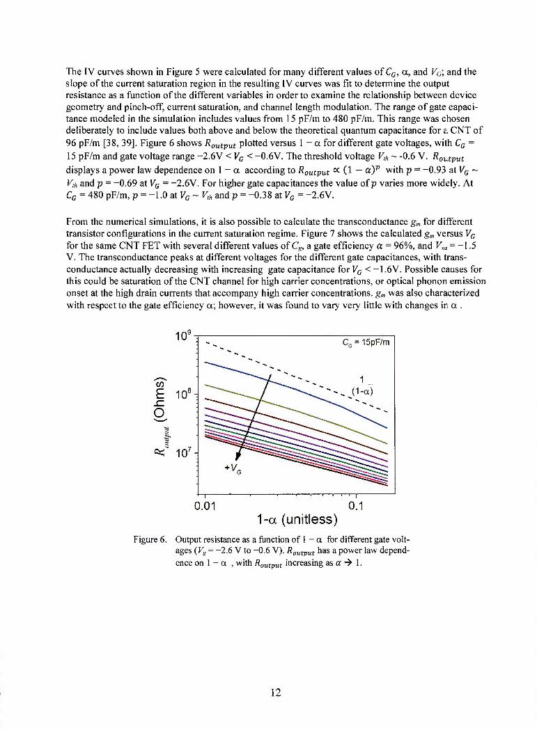
The IV curves shown in Figure 5 were calculated for many different values of CG, a, and Vo; and the slope of the current saturation region in the resulting IV curves was fit to determine the output resistance as a function of the different variables in order to examine the relationship between device geometry and pinch-off, current saturation, and channel length modulation. The range of gate capaci- tance modeled in the simulation includes values from 15 pF/m to 480 pF/m. This range was chosen deliberately to include values both above and below the theoretical quantum capacitance for £ CNT of 96 pF/m [38, 39]. Figure 6 shows Routput plotted versus I - a for different gate voltages, with CG = 15 pF/m and gate voltage range -2.6V <VG < -0.6V. The threshold voltage Vlh ~ -0.6 V. Routput displays a power law dependence on 1 - a according to R0UtVut « (1 — oc)v with p = -0.93 at VG ~ ¥& and p = -0.69 at VG = -2.6V. For higher gate capacitances the value of p varies more widely. At CG = 480 pF/m, p = -1.0 at VG ~ Vlh and p = -0.38 at VG = -2.6V.
From the numerical simulations, it is also possible to calculate the transconductance gm for different transistor configurations in the current saturation regime. Figure 7 shows the calculated gm versus VG
for the same CNT FET with several different values of Cg, a gate efficiency a = 96%, and Vsa = -1.5 V. The transconductance peaks at different voltages for the different gate capacitances, with trans- conductance actually decreasing with increasing gate capacitance for VG < -1.6V. Possible causes for this could be saturation of the CNT channel for high carrier concentrations, or optical phonon emission onset at the high drain currents that accompany high carrier concentrations. gm was also characterized with respect to the gate efficiency a; however, it was found to vary very little with changes in a .
.c O
IU :
108i
-^ Ce=15pF/m
107, ^'^SSiiiig *Ve ^^^^^^^^
i ' ■ ' i
0.01 0.1 1-a (unitless)
Figure 6. Output resistance as a function of 1 - a for different gate volt- ages {Vg = -2.6 V to -0.6 V). Routput has a power law depend- ence on 1 - a , with Routvut increasing as « -> 1.
12

12-
10-
8
3 6
2
CG = ■15pF/m • 30 pF/m ■ 60 pF/m •120pF/m ■240pF/m ■ 480 pF/m
VC = -1 5V SO
a = 0.96
-2.4 -2.0 -1.6 -1.2 -0.8
Figure 7. Transconductance gm versus gate voltage for several different gate capacitance values at a Fsrf = -1.5 V and a = 96%.
13

5. Conclusion
In conclusion, we have used the Landauer model used to calculate electrical transport in semicon- ducting carbon nanotube field-effect transistors at high source-drain voltages and for arbitrary gate voltages in the quantum capacitance limit. The model is used to fit experimental electrical transport data from suspended and substrate-bound single-nanotube CNT FETs. The model successfully repro- duces the subthreshold slope, on-off ratio, superthreshold roll-off, and current saturation at high volt- age. The model captures the physics of the channel length modulation effect, which results in finite output resistance in FETs. This model is a useful tool in characterizing, predicting, and optimizing electrical performance of carbon nanotube field-effect transistors for both digital and analog applications.
15

References
1. J. Baumgardner, et ai, "Inherent linearity in carbon nanotube field-effect transistors," Applied Physics Letters, 91, p. 052107, 2007.
2. J. Li, et ai, "Carbon nanotube sensors for gas and organic vapor detection," Nano Letters, 3, pp. 929-933, Jul 2003.
3. V. Sazonova, et ai, "A tunable carbon nanotube electromechanical oscillator," Nature, 431, p. 284, 2004.
4. P. J. Burke, "AC performance of nanoelectronics: towards a ballistic THz nanotube transistor," Solid-State Electronics, 48, pp. 1981-1986, 2004.
5. J. M. Marulanda, et ai, "Numerical modeling of the I-V characteristic of carbon nanotube field effect transistors (CNT-FETs)," in System Theory, 2008. SSST 2008. 40th Southeastern Symposium on, 2008, pp. 235-238.
6. M. Radosavljevic, et ai, "Drain voltage scaling in carbon nanotube transistors," Applied Physics Letters, 83, pp. 2435-2437, 2003.
7. A. Rahman, et ai, "Theory of ballistic nanotransistors," IEEE Trans. Electron Devices,, 50, pp. 1853-1864,2003.
8. S. Datta, Electronic Transport in Mesoscopic Systems: Cambridge Univ Pr, 1997.
9. A. Rahman, et al. (2011). FETToy. Available: http://nanohub.org/resources/fettov
10. L. Wei, et al, "Noniterative compact modeling for intrinsic carbon-nanotube FETs: Quantum capacitance and ballistic transport," IEEE Trans. Electron Devices, pp. 1-10, 2011.
11. T. J. Kazmierski, et ai, "Numerically efficient modeling of CNT transistors with ballistic and nonballistic effects for circuit simulation," IEEE Trans. Nanotechnology, 9, pp. 99-107, 2010.
12. A. Balijepalli, et al., "Compact modeling of carbon nanotube transistor for early stage process-design exploration," in Low Power Electronics and Design (ISLPED), 2007 ACM/IEEE International Symposium on, 2007, pp. 2-7.
13. A. Raychowdhury et al, "A circuit-compatible model of ballistic carbon nanotube field- effect transistors," IEEE Trans. Comput.-Aided Des. Integr. Syst. , 23, pp. 1411-1420, 2004.
14. Y. Zhao, et al, "Multiband mobility in semiconducting carbon nanotubes," IEEE electron device letters, 30, pp. 1078-1080, 2009.
17

15. Y.-F. Chen and M. S. Fuhrer, "Electric-field-dependent charge-carrier velocity in semiconducting carbon nanotubes," Physical Review Letters, 95, p. 236803, 2005.
16. A. Hazeghi, et al., "Schottky-barrier carbon nanotube field-effect transistor modeling," IEEE Trans. Electron Devices, 54, pp. 439-445, 2007.
17. S. Fregonese, et al., "Implementation of electron-phonon scattering in a CNTFET compact model," IEEE Trans. Electron Devices, 56, pp. 1184-1190, 2009.
18. S. O. Koswatta, et al., "Ballisticity of nanotube field-effect transistors: Role of phonon energy and gate bias," Applied Physics Letters, 89, pp. 023125-3, Jul. 2006.
19. N. Caudal, et al., "Kohn anomalies and non-adiabaticity in doped carbon nanotubes," Physical Review B, 75, pp. 115423-11, 2007.
20. J. C. Tsang, et al., "Doping and phonon renormalization in carbon nanotubes," Nature Nanotechnology, 2, pp. 725-730, Nov. 2007.
21. A. W. Bushmaker, et al., "Memristive Behavior Observed in Defected Single-Walled Carbon Nanotubes," IEEE Trans. Nanotechnology, Nov. 2009.
22. T. Yamada and J. i. Sone, "High-field electron transport in quantum wires studied by solution of the Boltzmann equation," Physical Review B, 40, pp. 6265-6271, 1989.
23. V. Perebeinos, et al., "Electron-Phonon Interaction and Transport in Semiconducting Carbon Nanotubes," Physical Review Letters, 94, p. 086802, Mar. 2005.
24. G. Pennington and N. Goldsman, "Semiclassical transport and phonon scattering of electrons in semiconducting carbon nanotubes," Physical Review B, 68, p. 045426, 2003.
25. A. Verma, et al., "Ensemble Monte Carlo transport simulations for semiconducting carbon nanotubes," Journal of Applied Physics, 97, pp. 114319-8, 2005.
26. J. Y. Park, et al, "Electron-phonon scattering in metallic single-walled carbon nanotubes," Nam Letters, 4, p. 517, Feb. 2004.
27. E. Pop, et al, "Negative differential conductance and hot phonons in suspended nanotube molecular wires," Physical Review Letters, 95, pp. 155505-8, Oct. 2005.
28. V. Derycke, et al, "Controlling doping and carrier injection in carbon nanotube transistors," Applied Physics Letters, 80, pp. 2773-2775, Apr. 2002.
29. F. Leonard and J. Tersoff, "Role of Fermi-level pinning in nanotube Schottky diodes," Physical Review Letters, 84, pp. 4693-4696, 2000.
30. S. Heinze, et al, "Carbon Nanotubes as Schottky Barrier Transistors," Physical Review Letters, 89, p. 106801,2002.
31. T. Yamada, "Analysis of submicron carbon nanotube field-effect transistors," Applied Physics Letters, 76, pp. 628-630, 2000.
18
32. Z. Zhang, et al, "Almost perfectly symmetric SWCNT-based CMOS devices and scaling," Acs Nano, 3, pp. 3781-3787, Nov 2009.
33. A. D. Franklin, et al, "Sub-10 nm carbon nanotube transistor," Nano Letters, 12, pp. 758-762, Feb 2012.
34. A. D. Franklin, et al, "Current scaling in aligned carbon nanotube array transistors with local bottom gating," Electron Device Letters, IEEE, 31, pp. 644-646, 2010.
35. C. Wang, et al, "Synthesis and device applications of high-density aligned carbon nanotubes using low-pressure chemical vapor deposition and stacked multiple transfer," Nano Research, 3, pp. 831-842, Dec 2010.
36. C. Wang, et al, "Device study, chemical doping, and logic circuits based on transferred aligned single-walled carbon nanotubes," Applied Physics Letters, 93, pp. 033101-033101-3, 2008.
37. C. Wang, et al, "Metal contact engineering and registration-free fabrication of complementary metal-oxide semiconductor integrated circuits using aligned carbon nanotubes," Acs Nano, 5, pp. 1147-1153, Feb 2011.
38. J. Dai, et al, "Measurements on quantum capacitance of individual single walled carbon nanotubes,'M^//e<iP^/c5 Leffera, 94, pp. 093114-093114-3, 2009.
39. P. J. Burke, "An RF circuit model for carbon nanotubes," IEEE Trans. Nanotechnology, 2, pp. 55-58, 2003.
19
Equipment Calibration Information
Techiiical R eports Addendum Asset Summary (jft\ A F" R (1 ^t PlU P F
TRAASID#: 2013112610452628764
Report Name: USC CNT FET measurements 2013112610452628764
Aerospace Report Number Start Date of Test: 2011-01-01 Created By: 28764 Bushmaker. Adam W 10:840900
End Date of Test: 2012-12-01 Fiist Aerospace Author y H: 28764 Bushmaker. Adam W Program:
Description: Keywords:
Manufacturer
Dale: CaJiEraton Cue Date: Comment: Oertftcate Mjmber: 1010-09.08 1011.1)9-02 HORMAL CM655:1283958279 1011J)5.17 IHS-Oi-U HOEMAL CM655:1306499575 1011J)3.16 mU-OS-U TMT-NORMAL 399l)8elb810te«lflI)coH96cl81880
'SUppat and Auxiliary Equipment are not calibrated.
21