Electrical Properties - IITKhome.iitk.ac.in/~anandh/MSE694/courseMSE694/NPTEL_Electrical... ·...
26
Electrical Properties Electrical Properties
Transcript of Electrical Properties - IITKhome.iitk.ac.in/~anandh/MSE694/courseMSE694/NPTEL_Electrical... ·...
Electrical PropertiesElectrical Properties
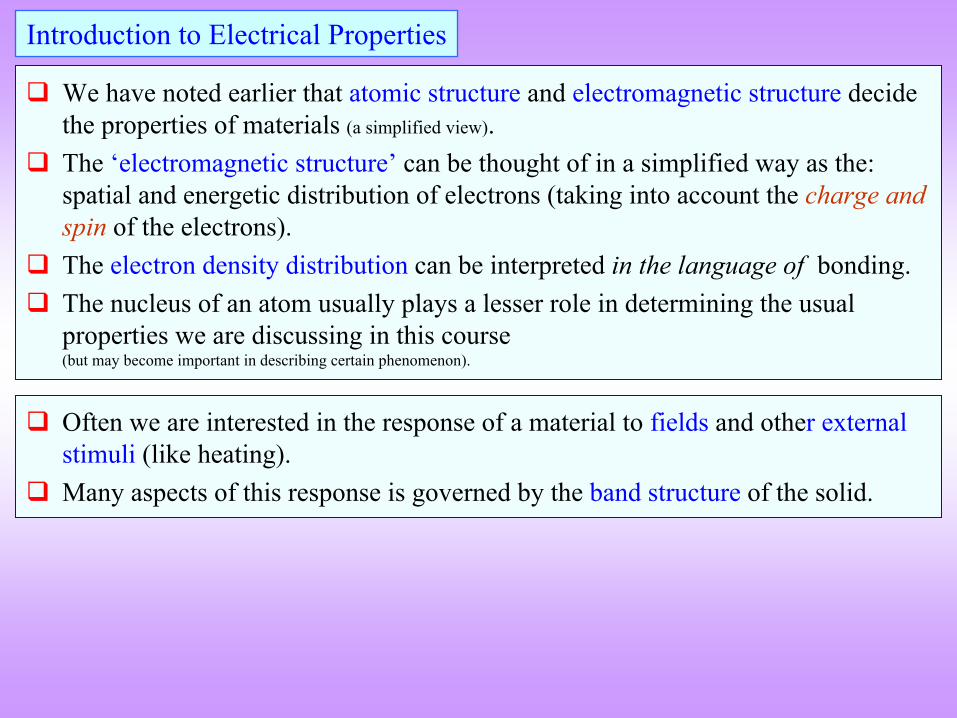
We have noted earlier that atomic structure and electromagnetic structure
decide the properties of materials (a simplified view).
The ‘electromagnetic structure’
can be thought of in a simplified way as the: spatial and energetic distribution of electrons (taking into account the charge and spin of the electrons).
The electron density distribution can be interpreted in the language of bonding.
The nucleus of an atom usually plays a lesser role in determining the usual properties we are discussing in this course (but may become important in describing certain phenomenon).
Introduction to Electrical Properties
Often we are interested in the response of a material to
fields
and other external stimuli (like heating).
Many aspects of this response is governed by the band structure
of the solid.
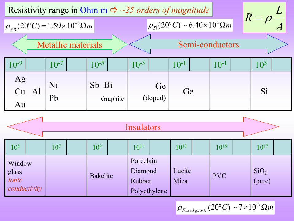
Resistivity range in Ohm m ~25 orders of magnitude
10-9 10-7 10-5 10-3 10-1 10-1 103
AgCu AlAu
NiPb
Sb
BiGraphite
Ge(doped)
Ge Si
105 107 109 1011 1013 1015 1017
Window
glass
Ionic
conductivity
Bakelite
PorcelainDiamondRubberPolyethylene
LuciteMica
PVCSiO2
(pure)
Metallic materials
Insulators
Semi-conductors
ALR
8(20 ) 1.59 10Ag C m 2(20 ) ~ 6.40 10Si C m
17(20 ) ~ 7 10Fused quartz C m
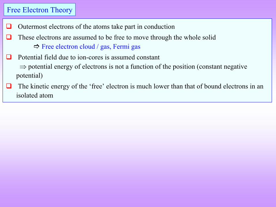
Free Electron Theory
Outermost electrons of the atoms take part in conduction
These electrons are assumed to be free to move through the whole solid
Free electron cloud / gas, Fermi gas
Potential field due to ion-cores is assumed constant potential energy of electrons is not a function of the position
(constant negative potential)
The kinetic energy of the ‘free’
electron is much lower than that of bound electrons in an isolated atom
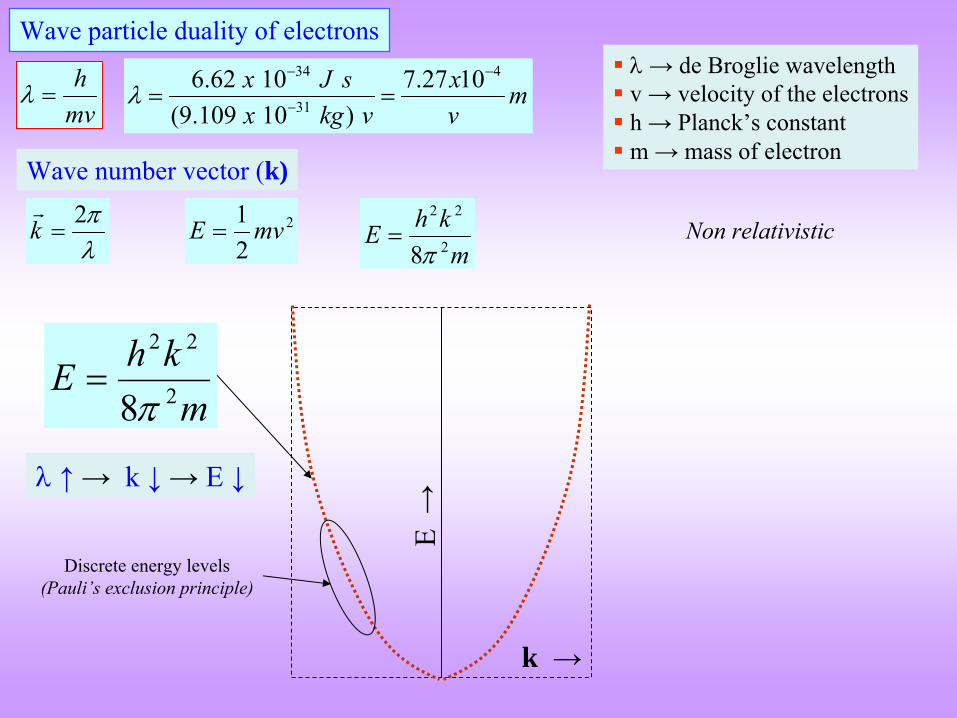
Wave particle duality of electrons
mvh
→ de Broglie
wavelength v → velocity of the electrons h → Planck’s constant m → mass of electron
34 4
31
6.62 10 7.27 10(9.109 10 )
x J s x mx kg v v
Wave number vector (k)
2
k
2
21 mvE Non relativistic
mkhE 2
22
8
mkhE 2
22
8
↑
→
k ↓
→ E ↓
E →
k →
Discrete energy levels(Pauli’s
exclusion principle)
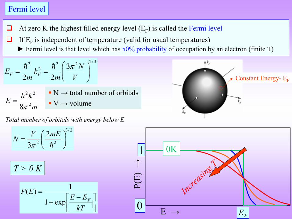
Fermi level
At zero K the highest filled energy level (EF
) is called the Fermi level
If EF
is independent of temperature (valid for usual temperatures) ► Fermi level is that level which has 50% probability
of occupation by an electron (finite T)
T > 0 K
kTEE
EPFexp1
1)(
P(E)
→
E →
1
FE
Increa
sing T
0K
0
2/32 2 22 3
2 2F FNE k
m m V
N → total number of orbitals V → volumem
khE 2
22
8
3/ 2
2 2
23V mEN
Total number of orbitals with energy below E
Constant Energy-
EF
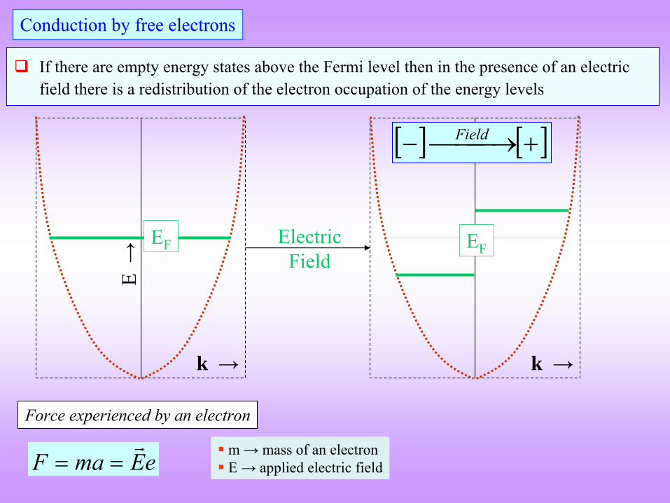
Conduction by free electrons
If there are empty energy states above the Fermi level then in the presence of an electric field there is a redistribution of the electron occupation of the energy levels
E →
k → k →
Field
EF EFElectric
Field
eEmaF
Force experienced by an electron
m → mass of an electron E → applied electric field
Vel
ocity
→
time →
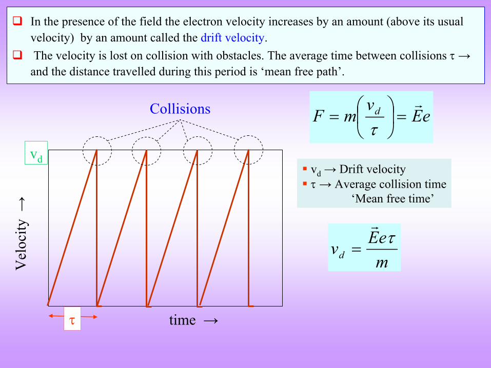
vd
Collisions
In the presence of the field the electron velocity increases by an amount (above its usual velocity) by an amount called the drift velocity.
The velocity is lost on collision with obstacles. The average time between collisions
→
and the distance travelled
during this period is ‘mean free path’.
eEv
mF d
vd
→ Drift velocity
→ Average collision time
‘Mean free time’
meEvd
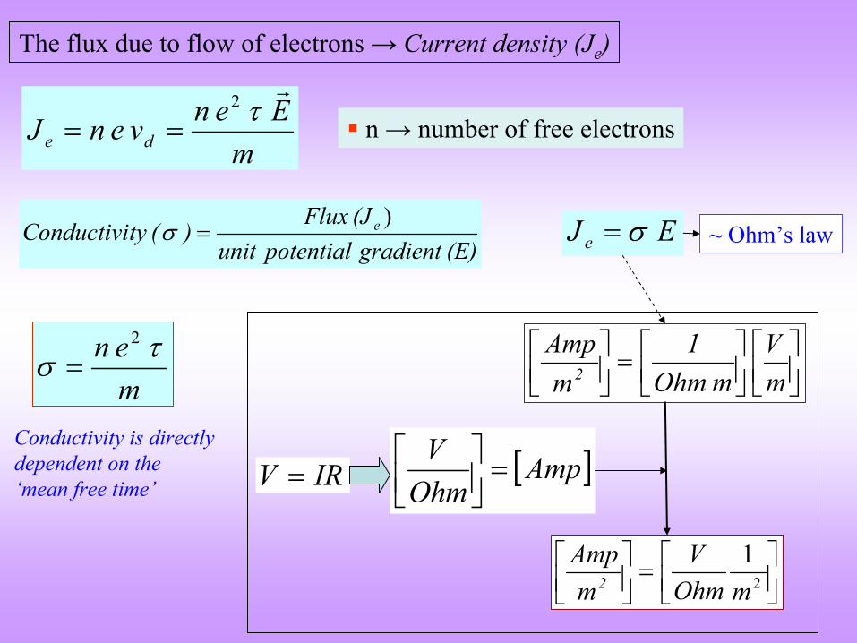
The flux due to flow of electrons → Current density (Je
)
mE e nv e nJ de
2
n → number of free electrons
(E) gradient potential unit(J Flux
)(ty Conductivi e ) E J e
m e n
2
mV
m Ohm1
mAmp
2
IRV AmpOhm
V
2
1mOhm
Vm
Amp2
~ Ohm’s law
Conductivity is directly dependent on the ‘mean free time’
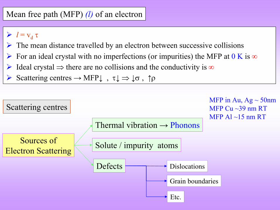
Mean free path (MFP) (l)
of an electron
l
= vd
The mean distance travelled
by an electron between successive collisions
For an ideal crystal with no imperfections (or impurities) the MFP
at 0 K is
Ideal crystal there are no collisions and the conductivity is
Scattering centres
→ MFP↓
, ↓
↓
, ↑
Scattering centres
Sources of Electron Scattering Solute / impurity atoms
Defects
Thermal vibration → Phonons
Grain boundaries
Dislocations
Etc.
MFP
in Au, Ag ~ 50nmMFP
Cu ~39 nm RTMFP
Al ~15 nm RT
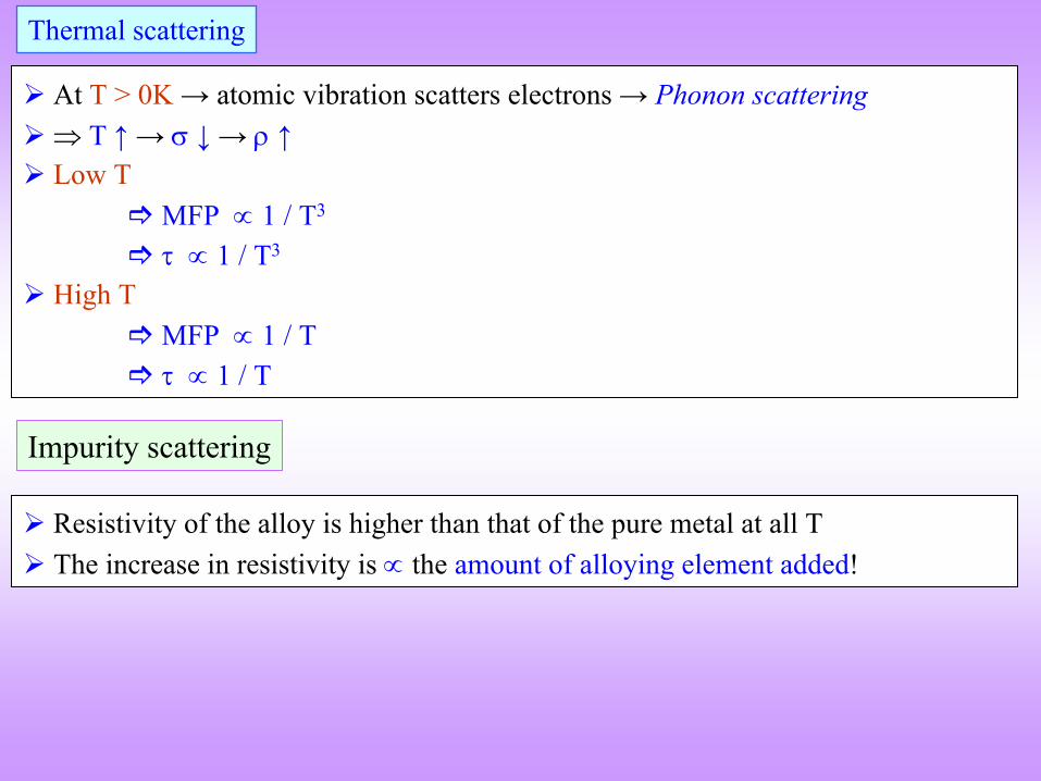
Thermal scattering
At T > 0K
→ atomic vibration scatters electrons → Phonon scattering T ↑
→
↓
→
↑
Low T
MFP
1 / T3
1 / T3
High T
MFP
1 / T
1 / T
Impurity scattering
Resistivity of the alloy is higher than that of the pure metal at all T The increase in resistivity is
the amount of alloying element added!
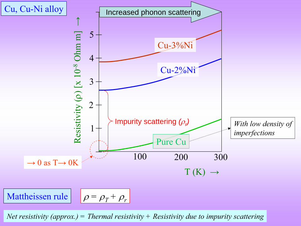
Res
istiv
ity (
) [x
10-8
Ohm
m] →
T (K) →
Cu, Cu-Ni alloy
100 200 300
1
2
3
4
5
Cu-2%Ni
Cu-3%Ni
→ 0 as T→ 0K
With low density of
imperfections
Pure Cu
Increased phonon scattering
Impurity scattering (r )
Mattheissen
rule = T
+ r
Net resistivity (approx.) = Thermal resistivity + Resistivity due to impurity scattering
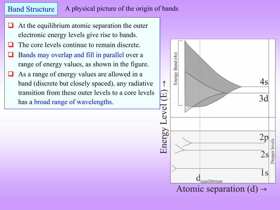
At the equilibrium atomic separation the outer electronic energy levels give rise to bands.
The core levels continue to remain discrete.
Bands may overlap and fill in parallel
over a range of energy values, as shown in the figure.
As a range of energy values are allowed in a band (discrete but closely spaced), any radiative
transition from these outer levels to a core levels has a broad range of wavelengths.
Band Structure A physical picture of the origin of bands
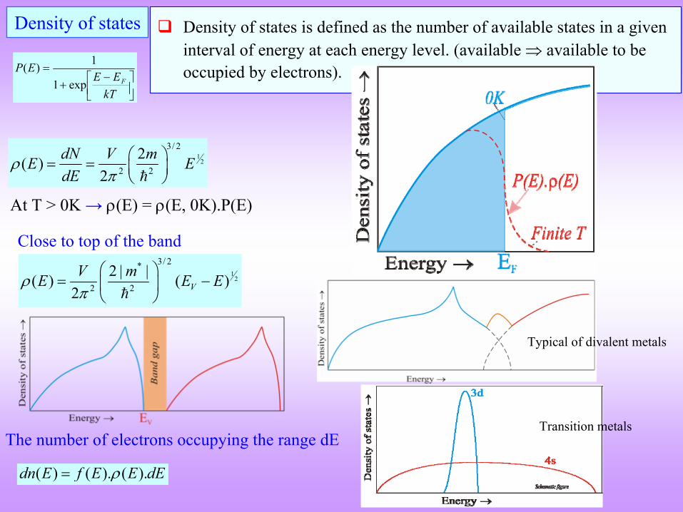
Density of states is defined as the number of available states in a given interval of energy at each energy level. (available available to be occupied by electrons).
Density of states
12
3/ 2
2 2
2( )2
dN V mE EdE
kTEE
EPFexp1
1)(
At T > 0K → (E) = (E, 0K).P(E)
12
3/ 2*
2 2
2 | |( ) ( )2 VV mE E E
Close to top of the band
Typical of divalent metals
Transition metalsThe number of electrons occupying the range dE
( ) ( ). ( ).dn E f E E dE
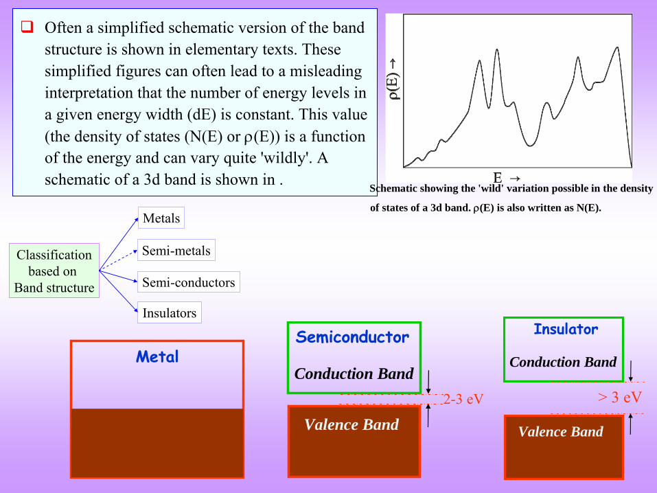
Often a simplified schematic version of the band structure is shown in elementary texts. These simplified figures can often lead to a misleading interpretation that the number of energy levels in a given energy width (dE) is constant. This value (the density of states (N(E) or (E)) is a function of the energy and can vary quite 'wildly'. A schematic of a 3d band is shown in .
Schematic showing the 'wild' variation possible in the density
of states of a 3d band. (E) is also written as N(E).
> 3 eV
Valence Band
Conduction Band
Insulator
2-3 eV
Valence Band
Conduction Band
SemiconductorMetal
Classificationbased on
Band structure
Semi-metals
Semi-conductors
Metals
Insulators
Electrical Properties of NanomaterialsElectrical Properties of Nanomaterials
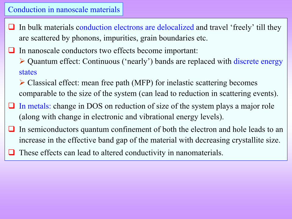
In bulk materials conduction electrons are delocalized and travel ‘freely’
till they are scattered by phonons, impurities, grain boundaries etc.
In nanoscale conductors two effects become important:
Quantum effect: Continuous (‘nearly’) bands are replaced with discrete energy states
Classical effect: mean free path (MFP) for inelastic scattering becomes comparable to the size of the system (can lead to reduction in scattering events).
In metals: change in DOS on reduction of size of the system plays a major role (along with change in electronic and vibrational energy levels).
In semiconductors quantum confinement of both the electron and hole leads to an increase in the effective band gap of the material with decreasing crystallite size.
These effects can lead to altered conductivity in nanomaterials.
Conduction in nanoscale materials
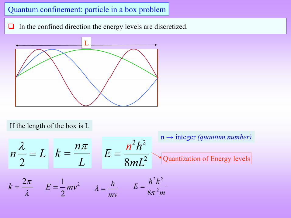
In the confined direction the energy levels are discretized.
Quantum confinement: particle in a box problem
L
If the length of the box is L
Ln 2
n → integer (quantum number)2 2
28n hEmL
L
nk Quantization of Energy levels
2k
212
E mvmvh
mkhE 2
22
8
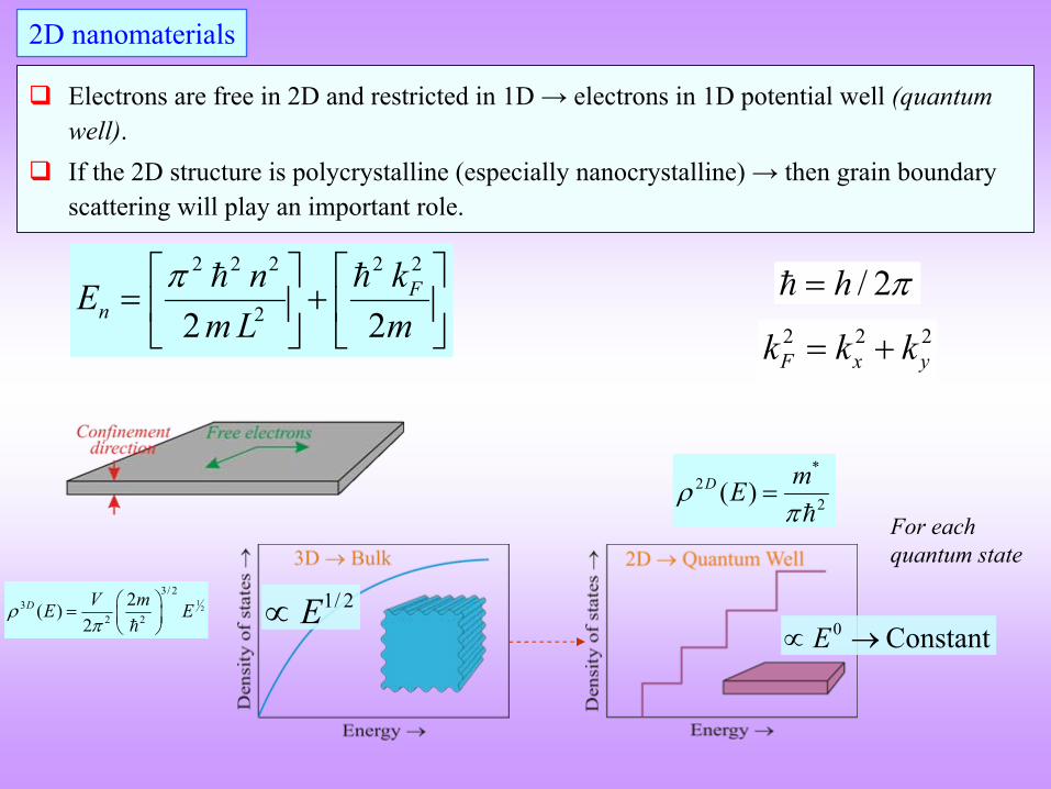
Electrons are free in 2D and restricted in 1D → electrons in 1D potential well (quantum well).
If the 2D structure is polycrystalline (especially nanocrystalline) → then grain boundary scattering will play an important role.
2D nanomaterials
2 2 2 2 2
22 2F
nn kE
m L m
/ 2h 2 2 2F x yk k k
1/ 2E 0 ConstantE
*2
2( )D mE
12
3/ 23
2 2
2( )2
D V mE E
For each quantum state
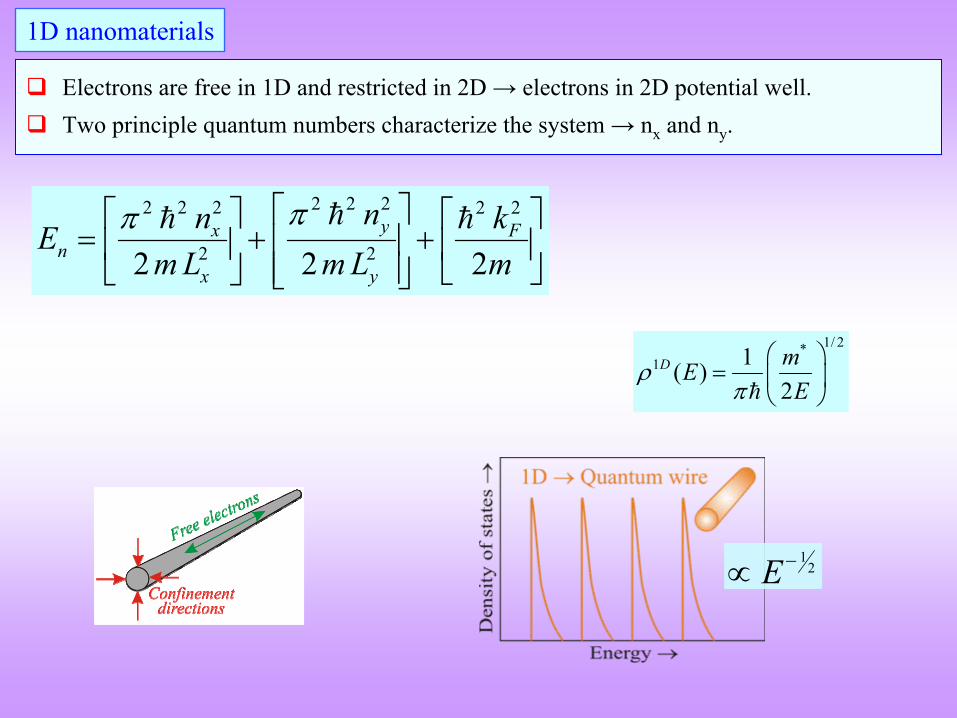
Electrons are free in 1D and restricted in 2D → electrons in 2D potential well.
Two principle quantum numbers characterize the system → nx
and ny
.
1D nanomaterials
2 2 22 2 2 2 2
2 22 2 2yx F
nx y
nn kEm L m L m
1/ 2*1 1( )
2D mE
E
12E
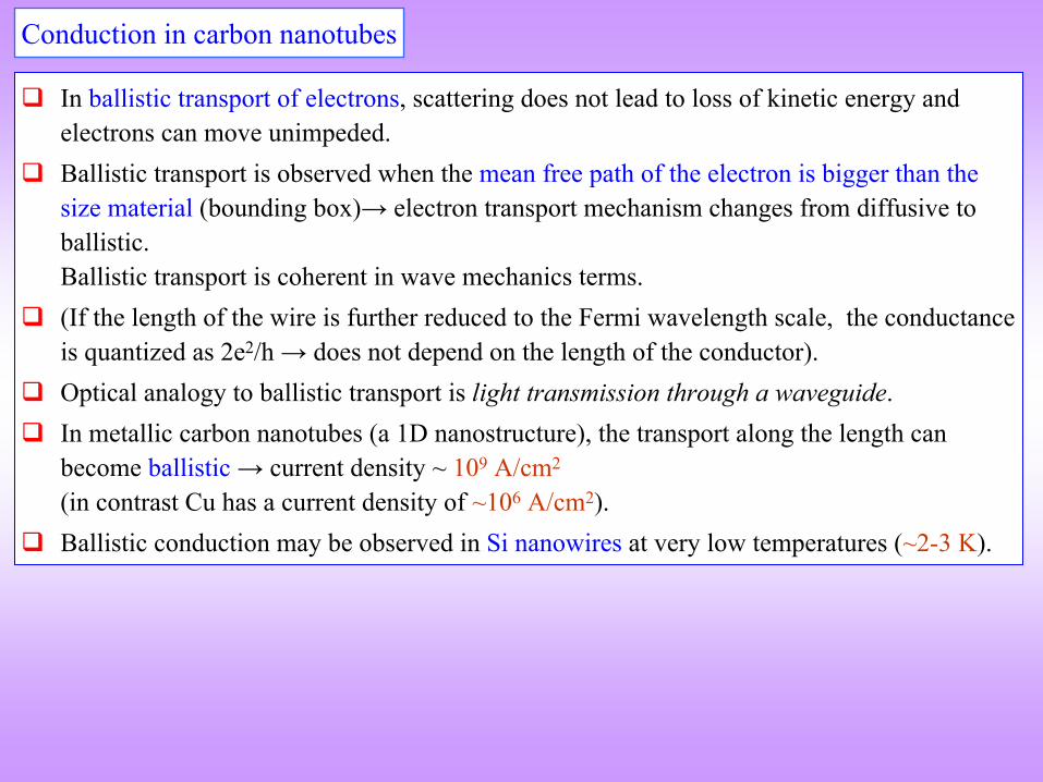
In ballistic transport of electrons, scattering does not lead to loss of kinetic energy and electrons can move unimpeded.
Ballistic transport is observed when the mean free path of the electron is bigger than the size material
(bounding box)→ electron transport mechanism changes from diffusive to ballistic. Ballistic transport is coherent in wave mechanics terms.
(If the length of the wire is further reduced to the Fermi wavelength scale, the conductance is quantized as 2e2/h → does not depend on the length of the conductor).
Optical analogy to ballistic transport is light transmission through a waveguide.
In metallic carbon nanotubes
(a 1D nanostructure), the transport along the length can become ballistic
→ current density ~ 109
A/cm2
(in contrast Cu has a current density of ~106
A/cm2).
Ballistic conduction may be observed in Si
nanowires
at very low temperatures (~2-3 K).
Conduction in carbon nanotubes
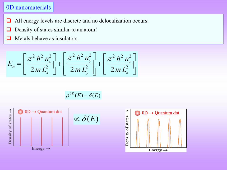
All energy levels are discrete and no delocalization occurs.
Density of states similar to an atom!
Metals behave as insulators.
0D nanomaterials
2 2 22 2 2 2 2 2
2 2 22 2 2yx z
nx y z
nn nEm L m L m L
( )E
0 ( ) ( )D E E
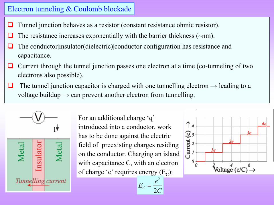
Tunnel junction behaves as a resistor (constant resistance ohmic
resistor).
The resistance increases exponentially with the barrier thickness (~nm).
The conductor|insulator(dielectric)|conductor
configuration has resistance and capacitance.
Current through the tunnel junction passes one electron at a time (co-tunneling of two electrons also possible).
The tunnel junction capacitor is charged with one tunnelling
electron → leading to a voltage buildup → can prevent another electron from tunnelling.
Electron tunneling & Coulomb blockade
For an additional charge ‘q’
introduced into a conductor, work has to be done against the electric field of preexisting charges residing on the conductor. Charging an island with capacitance C, with an electron of charge ‘e’
requires energy (EC
):2
2CeEC
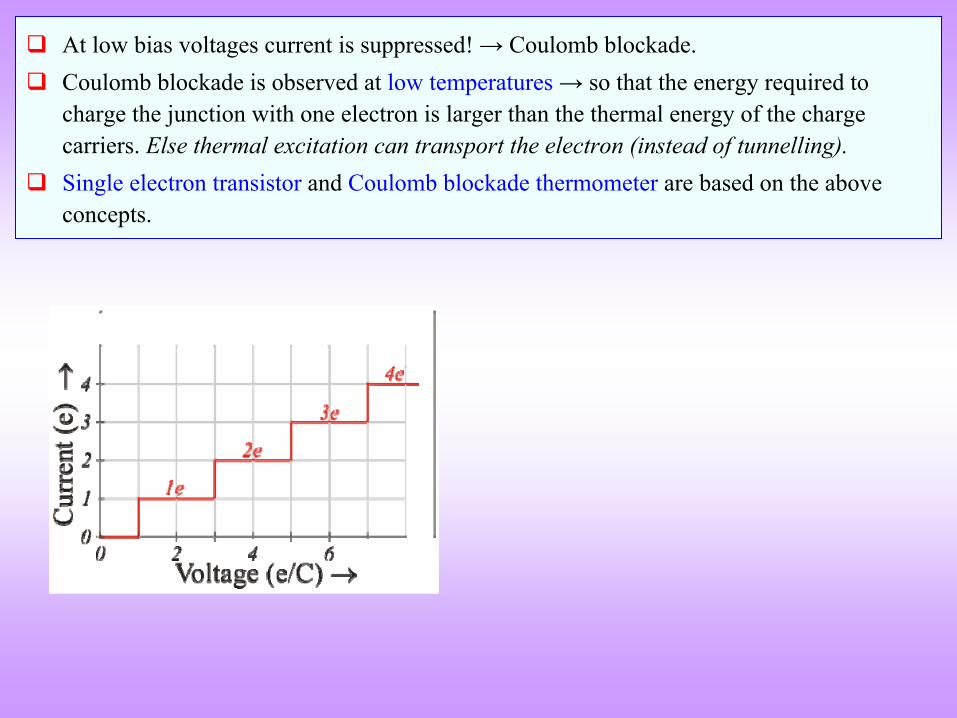
At low bias voltages current is suppressed! → Coulomb blockade.
Coulomb blockade is observed at low temperatures → so that the energy required to charge the junction with one electron is larger than the thermal
energy of the charge carriers. Else thermal excitation can transport the electron (instead of tunnelling).
Single electron transistor and Coulomb blockade thermometer
are based on the above concepts.
End
Example: quantum dot based field effect transistor (FET)