Electrical, Optical, Mechanical Study of Differences in ...Electrical, Optical, Mechanical Study of...
15
Electrical, Optical, Mechanical Study of Differences in ZnO Based TCOs and ITO Thin Films Jing Yang SCI Engineered Materials, Inc The Science of Engineered Materials TM
Transcript of Electrical, Optical, Mechanical Study of Differences in ...Electrical, Optical, Mechanical Study of...

Electrical, Optical, Mechanical Study of Differences in ZnO Based TCOs and ITO
Thin Films
Jing YangSCI Engineered Materials, Inc
The Science of Engineered MaterialsTM
History of SCI
Founded in 1987 by Prof. Funk ( Ohio State University) as Superconductive Components, Inc. in Columbus, OH. Changed name to SCI Engineered Materials, Inc. in 2007
Initially focused on R&D with high temperature superconducting materialsand devices
Developed manufacturing capabilities to produce advanced ceramiccompositions for sputtering targets
Manufacture products for diverse global markets
Continue to leverage manufacturing capabilities, intellectual property andproprietary knowledge into complementary growth markets
Proprietary to SCI Engineered Materials 2

Basic Properties of ZnO Based TCO vs. ITO
Proprietary to SCI Engineered Materials 3
ITO ZnO based TCO
90%In2O3/10%SnO2 ChemistryZnO: Al (AZO);
ZnO:Ga (GZO) and others
Rocksalt(Cubic based)
Crystal structure
Wurtzite(Hexagonal based)
PVD (sputtering)Mass
productiondeposition
PVD (sputtering)
Sn doping and Ovacancies
Conductivemechanism
Defects, vacancies (O deficiencies)
1-2x10⁻⁴ohm.cmpost anneal
Thin filmresistivity
Thickness dependant3x10-4 ohm.cm for more than 400nm
High Visible light transmission High
Partial pressure of O2 is very critical
Sputteringcondition Ar only
Materion Technical Paper

TCO Application – DisplayAZO (GZO) and ITO as electrode in four modes:
SCI sponsored research successfully replace ITO with AZO/GZO in all four LC modes (Kent State Liquid Crystal Institute)
Proprietary to SCI Engineered Materials4
Twisted Nematic (TN) Vertical Aligned (VA): In plane Switch (IPS) Fringe Field Switch (FFS)
Contrast Ratio 1801:1 1812:1 3000:1 3000:1 1300:1 1100:1 1500:1 500:1
turn on/ms 6.2 6.1 400 440 20.7 17.5 28.9 28.3
Und
er P
OM
Illustration Credit to: FFS Technology

TCO Application - PDLC ElectrodePDLC- Polymer Dispersed Liquid Crystal:
Application: Smart curtains
We used AZO to displace ITO as electrode in PDLC cell
AZO: ~200ohm/sqr, 100nm
Proprietary to SCI Engineered Materials 5Image taken from internet

Optimize Sputtering Condition for TCO Thin Film Sputtering AZO and ITO in-house: In-house DC sputtering: MRC, 5E-6Torr
Proprietary to SCI Engineered Materials 6
Time(s)
Thickness(nm)
Rs(Ω/)
ρ(Ω.cm)
53 120 145 1.7 x10⁻³
70 170 95 1.5 x10⁻³
106 250 57 1.4 x10⁻³
Ar+5%O2
Thickness(nm)
Rs(Ω/)
ρ(Ω.cm)
14 sccm 150 45 6.8x10⁻⁴
18 sccm 150 42 6.3x10⁻⁴
22 sccm 150 49 7.3 x10⁻⁴
AZO thin film Resistivity with different thickness3kw, Ar 9E-3Torr
ITO thin film Resistivity with different O2 flow 1kw, Ar 34 sccm
Z Ma et al, Nanophotonics 2015
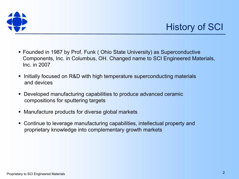
Post Annealing for AZO and GZO:
Annealing Temperature for ITO: 220-260oC Significant lower annealing T for AZO than ITO Little anneal needed for GZO thin film to achieve low resistance AZO and GZO is more compatible with low temperature process
Low Annealing T for AZO and GZO
Proprietary to SCI Engineered Materials 7
AZO annealing study GZO annealing study
GZO before anneal
0 20 40 60 80 100 120 140 160 180 200 220-40
-30
-20
-10
0
10
20
30
Decr
ease
per
cent
age
(%)
Annealing Temp (C)
Rs
160nm 64Ω/
Optimized in-house ITO annealing T
210nm 63Ω/

Optical Comparison between AZO and ITO
Visible (400nm-700nm) – Display Industry:
• The transmission of AZO in visible range is very high but needs optimization due to thickness fringes. (~130nm film renders highest visible transmittance)
• To achieve same visible transmittance, ITO needs be significant thinner than AZO.Proprietary to SCI Engineered Materials
8
AZO visible T% vs. film thickness
Sample Thickness Rs T%(400-700nm)
AZO 130nm 70Ω/sq >96%ITO* 30nm 80Ω/sq 96.5%
* Commercially available ITO thin film on glass
300 400 500 600 700 800 900 10000
20
40
60
80
100
ZnO-3(115nm) ZnO-4(120nm)
Tran
smitt
ance
(%)
Wavelength (nm)

Optical Comparison between AZO and ITO
Visible to near IR – Solar Industry :
• Depends on the specific solar cell, when low temperature process needed, AZO has higher transmission in the visible to near IR wavelength.
IR:
• AZO has lower plasma wavelength than ITO due to a high carrier concentration thus reflecting more in the IR wavelength
• It is specifically beneficial for low E glass industry
Proprietary to SCI Engineered Materials9
Sample Thickness R T%(400-1200nm)
AZO 250nm 56Ω/sq 87.3%AZO-a 250nm 42Ω/sq 90.4%
ITO 185nm 40Ω/sq 88.9%
Wavelength (nm)Tr
ansm
ittan
ce ()
% ITO
AZO
AZO annealed
Annealed AZO vs. ITO with same Rs

UV:
AZO absorb more UV light than ITO due to a smaller band gap which is tunable with different doping level.
It is attractive to protect some organic device from UV damage.
Proprietary to SCI Engineered Materials10
300 400 500 600 700 800 900 10000
20
40
60
80
100
ITO 30nm AZO 115nm AZO 210nm AZO 310nm
Tran
smitt
ance
(%)
Wavelength (nm) Eg1%AZO 3.55eV
1.5%AZO 3.58eV
2%AZO 3.60eV
y = 0.0127x - 0.0457
Tran
smitt
ance
%
Wavelength (nm)
Optical Comparison between AZO and ITO

Resistance changes of thin film after bending (tensile)
The resistance of AZO/Ag is stable on PEN
Ag is very thin (<5nm) as oxygen/humidity barrier
AZO is mechanically more stable under bending test.
Proprietary to SCI Engineered Materials11
Mechanical Property Comparison: Bending test
G. Torrisi et. al. Solar Energy Materials and Solar cell, 2017
R. Liu et al, Solar Materials and Solar Cell, 2019
Coalesced film
Columnar film

Proprietary to SCI Engineered Materials12
SummaryProperties ITO Metal doped ZnOResistivity Low Higher
Annealing T High Low
Thickness to achieve similar Rs Thin Thick (x2)
Transmittance in visible High High
Transmittance in IR High Low
Cut off in UV Lower wavelength Higher wavelength
Mechanical stability Low High
Cost/unit weight $$$ $
Raw material availability Low High
AZO STD- 94%TD AZO HD – 98%TD

Special thanks to:
13
Any questions?

Stability study of ITO and AZO on flexible thin film:
The resistance of AZO on PET increases 100% within 2 weeks of exposure in air
The resistance of AZO on PEN is better but still increased 40% after 60 days.
ITO on PET is more stable than AZO on PET and increases less than 10% after 5 months.
AZO/Ag is very stable on PEN.
Proprietary to SCI Engineered Materials
14
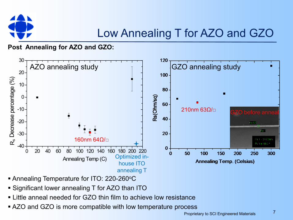
Thin Film Properties Comparison between AZO and ITO
R. Liu et al, Solar Materials and Solar Cell, 2019
Coalesced film
Columnar film
Oxygen, Humidity
Oxygen, Humidity when on flexible substrate such as PET and PEN
AZO/GZO on PET in house:
The Rs is largely depend on how flat the PET surface is.
With edge taping to the backing plate, it doesn’t render uniform nor low resistance comparing to that on glass substrate. Proprietary to SCI Engineered Materials
15
8”*12”
AZO/GZO on PET R2R with collaborators:
Collaborator 1: - ~160nm, Rs~300Ω/sq GZO on PET and glass.
- ρ: 4.8*10-3Ω-cm.(~310nm, Rs~125Ω/sq, ρ: 3.9*10-3ohm-cm)- T:88-90%- Base pressure ~1x10⁻⁵torr
We think the high Rs is due to high base pressure degas of PET roll.
Collaborator 2: Power: 3kw DC & DC pulse; Base pressure: 3-
4x10⁻⁶torr Substrates: slide & film ST505 (DuPont 5mil PET)Film: 200nm 2%AZOOn glass: 1.3-1.6 x 10⁻³ Ω-cmOn PET: 1.2-1.9x on glass
Thin Film Properties Comparison between AZO and ITO